US5270821A - Video display adjustment and on-screen menu system - Google Patents
Video display adjustment and on-screen menu systemDownload PDFInfo
- Publication number
- US5270821A US5270821AUS07/796,411US79641191AUS5270821AUS 5270821 AUS5270821 AUS 5270821AUS 79641191 AUS79641191 AUS 79641191AUS 5270821 AUS5270821 AUS 5270821A
- Authority
- US
- United States
- Prior art keywords
- display
- video display
- memory
- character
- microcontroller
- Prior art date
- Legal status (The legal status is an assumption and is not a legal conclusion. Google has not performed a legal analysis and makes no representation as to the accuracy of the status listed.)
- Expired - Lifetime
Links
- 230000015654memoryEffects0.000claimsdescription61
- 230000000007visual effectEffects0.000claimsdescription20
- 238000000034methodMethods0.000claimsdescription19
- 230000001360synchronised effectEffects0.000abstractdescription8
- 238000012360testing methodMethods0.000description6
- 238000010586diagramMethods0.000description5
- 241000226585Antennaria plantaginifoliaSpecies0.000description4
- 240000000136Scabiosa atropurpureaSpecies0.000description4
- 239000002131composite materialSubstances0.000description4
- 239000003990capacitorSubstances0.000description3
- 230000008859changeEffects0.000description3
- 230000001276controlling effectEffects0.000description3
- 230000007613environmental effectEffects0.000description3
- 230000006870functionEffects0.000description3
- 230000005055memory storageEffects0.000description3
- 241000238876AcariSpecies0.000description2
- 102000052922Large Neutral Amino Acid-Transporter 1Human genes0.000description2
- 108091006232SLC7A5Proteins0.000description2
- 238000005516engineering processMethods0.000description2
- 230000006872improvementEffects0.000description2
- 238000012986modificationMethods0.000description2
- 230000004048modificationEffects0.000description2
- 102100024061Integrator complex subunit 1Human genes0.000description1
- 101710092857Integrator complex subunit 1Proteins0.000description1
- MENQCIVHHONJLU-FZCSVUEKSA-N[(3s,5s,8r,9s,10s,13s,14s,17s)-17-acetyl-10,13-dimethyl-2,3,4,5,6,7,8,9,11,12,14,15,16,17-tetradecahydro-1h-cyclopenta[a]phenanthren-3-yl] hydrogen sulfateChemical compoundC([C@@H]1CC2)[C@@H](OS(O)(=O)=O)CC[C@]1(C)[C@@H]1[C@@H]2[C@@H]2CC[C@H](C(=O)C)[C@@]2(C)CC1MENQCIVHHONJLU-FZCSVUEKSA-N0.000description1
- 230000000295complement effectEffects0.000description1
- 238000010276constructionMethods0.000description1
- 230000001419dependent effectEffects0.000description1
- 230000009977dual effectEffects0.000description1
- 230000000694effectsEffects0.000description1
- 238000004519manufacturing processMethods0.000description1
- 230000007246mechanismEffects0.000description1
- 238000003825pressingMethods0.000description1
- 230000001105regulatory effectEffects0.000description1
- 230000004044responseEffects0.000description1
- 238000001228spectrumMethods0.000description1
- 230000003068static effectEffects0.000description1
- 230000007704transitionEffects0.000description1
Images


Classifications
- G—PHYSICS
- G09—EDUCATION; CRYPTOGRAPHY; DISPLAY; ADVERTISING; SEALS
- G09G—ARRANGEMENTS OR CIRCUITS FOR CONTROL OF INDICATING DEVICES USING STATIC MEANS TO PRESENT VARIABLE INFORMATION
- G09G1/00—Control arrangements or circuits, of interest only in connection with cathode-ray tube indicators; General aspects or details, e.g. selection emphasis on particular characters, dashed line or dotted line generation; Preprocessing of data
- G09G1/06—Control arrangements or circuits, of interest only in connection with cathode-ray tube indicators; General aspects or details, e.g. selection emphasis on particular characters, dashed line or dotted line generation; Preprocessing of data using single beam tubes, e.g. three-dimensional or perspective representation, rotation or translation of display pattern, hidden lines, shadows
- G09G1/14—Control arrangements or circuits, of interest only in connection with cathode-ray tube indicators; General aspects or details, e.g. selection emphasis on particular characters, dashed line or dotted line generation; Preprocessing of data using single beam tubes, e.g. three-dimensional or perspective representation, rotation or translation of display pattern, hidden lines, shadows the beam tracing a pattern independent of the information to be displayed, this latter determining the parts of the pattern rendered respectively visible and invisible
- G09G1/16—Control arrangements or circuits, of interest only in connection with cathode-ray tube indicators; General aspects or details, e.g. selection emphasis on particular characters, dashed line or dotted line generation; Preprocessing of data using single beam tubes, e.g. three-dimensional or perspective representation, rotation or translation of display pattern, hidden lines, shadows the beam tracing a pattern independent of the information to be displayed, this latter determining the parts of the pattern rendered respectively visible and invisible the pattern of rectangular co-ordinates extending over the whole area of the screen, i.e. television type raster
- G—PHYSICS
- G09—EDUCATION; CRYPTOGRAPHY; DISPLAY; ADVERTISING; SEALS
- G09G—ARRANGEMENTS OR CIRCUITS FOR CONTROL OF INDICATING DEVICES USING STATIC MEANS TO PRESENT VARIABLE INFORMATION
- G09G5/00—Control arrangements or circuits for visual indicators common to cathode-ray tube indicators and other visual indicators
- G09G5/003—Details of a display terminal, the details relating to the control arrangement of the display terminal and to the interfaces thereto
- G—PHYSICS
- G09—EDUCATION; CRYPTOGRAPHY; DISPLAY; ADVERTISING; SEALS
- G09G—ARRANGEMENTS OR CIRCUITS FOR CONTROL OF INDICATING DEVICES USING STATIC MEANS TO PRESENT VARIABLE INFORMATION
- G09G2320/00—Control of display operating conditions
- G09G2320/08—Arrangements within a display terminal for setting, manually or automatically, display parameters of the display terminal
Definitions
- the present inventionrelates to video display systems, and more particularly, to using on-screen menus in adjusting multi-frequency cathode ray tube (CRT) displays.
- CRTcathode ray tube
- Video displays incorporating CRT systemsprovide information to and receive information from computer systems.
- Early video displaystypically were single-frequency displays: the video adaptor card that operated the display (by sending information from the computer to the display) used a single horizontal scanning frequency tuned to that of the display.
- a card fabricated for a particular single-frequency displayoften will not work with other displays.
- Multi-frequency video displaysrepresent an important improvement in video display technology, for a single display system can be attached to a wide variety of video adaptor cards.
- the multi-frequency displaycan tune itself to the horizontal frequency of the attached adaptor card, and synchronize the display to the information sent from the adaptor card.
- While multi-frequency displaysprovide a great improvement over single-frequency displays, and allow versatile connections of displays and adaptor cards, these displays exacerbate problems common to video displays in general.
- Most video displaysprovide some form of adjustments for users.
- a panel of knobs and buttons connected to potentiometers or other electrical switchesallow the user to adjust various display characteristics. Contrast, brightness, and the horizontal and vertical image positions are some of the possible adjustments one can make. Since these adjustments are made manually using electromechanical devices, the adjustments are susceptible to slight shifts over time. Movement of the display, changes in ambient temperature and environmental vibrations can all alter carefully set adjustments.
- Multi-frequency displaysthat incorporate electromechanical user adjustments share these problems of misadjustment.
- these displaysmultiply adjustment problems for each new frequency mode available.
- Multi-frequency displayspresent further manufacturing difficulties.
- each video displaypossesses a number of internal controls that precisely adjust the display.
- These internal controlsare preset at the factory by a human operator comparing the display against a standard.
- multi-frequency displaysoften hive separate sets of these adjustments for each of several principle frequency bands. Each of these adjustment sets must then be hand-adjusted by a factory operator. Again, the electro-mechanical nature of the controls allows for gradual drift in their adjustment.
- An improved video display adjustment apparatus and methodshould allow the factory to quickly set all internal controls for a monitor, without operator intervention.
- the improved apparatus and methodshould also allow end-users to easily change display characteristics, or reset the characteristics back to those specified at the factory.
- the method and apparatusshould also maintain the video display characteristics despite thermal, mechanical or other environmental changes.
- the improved method and apparatusshould provide techniques and apparatus applicable to a wide range of video display devices, including CRTS, LCDs and electro-luminescent displays.
- the inventionshould provide a simple and cost-effective technology for easily and accurately changing and maintaining the characteristics of any video display.
- a video display adjustment and on-screen menu systemcombines a microcontroller and erasable EPROM memory with on-screen menu display generation to allow users to change display parameters without making any electromechanical adjustments.
- the microcontrollereffects display changes through display adjustment circuitry, enabling digital control over display parameters.
- the present inventionincorporates a novel video clock to ensure accurate synchronization of the on-screen menu to any horizontal signal received by the video display.
- the userenters commands to the microcontroller by pressing a set of buttons, or other similar input devices on the video display, in response to selections displayed by the on-screen menu.
- User commandsare latched and accessed by the microcontroller; and changes to display parameters made by the user are written to an EEPROM memory that in the preferred embodiment can store a set of adjustments for each of up to 32 possible operational frequency modes.
- the display adjustment circuitryincludes a digital-to-analog converter (DAC) that converts display parameters provided by the microcontroller in digital form to an analog signal that is multiplexed via a set of analog switches to a plurality of sample-and-hold circuits. Upon start-up, these circuits are loaded with and maintain current display parameters, until changed by the user.
- DACdigital-to-analog converter
- the on-screen menu generation circuitryincludes a set of column and row counters that keep track of the next menu location to be displayed. Because higher horizontal frequencies indicate higher resolutions, the characters of the menu are adjusted to maintain a relatively constant character size.
- the microcontrollerdetermines how many vertical lines are being displayed, and then a character size control block determines whether to double the number of times a pixel line of a given character is repeated, essentially elongating the character. When a line repeats, the row counter does not increment despite the fact that another horizontal synch signal was received.
- the current column and row valuesaddress a display memory, loaded by the microcontroller, that contains the menu information. As each menu character is read out of the display memory at the appropriate column and row, its visual representation is provided by a character PROM and then sent to a shift register where each pixel is clocked out to a video drive.
- the video clockgoverns the operation of the column and row counters, and that of the shift register, and thereby the flow of menu information to the display.
- the novel video clock of the present inventionstops operation for a given scan line when the end of the column counters are reached for each menu line.
- the video clockresumes its operation when the next horizontal synch signal occurs. In this way, the menu remains intact and readable regardless of what horizontal frequency the display currently uses.
- the present inventionallows users to easily and precisely adjust the parameters of a multi-frequency video display without adjusting electromechanical inputs. Once parameters are chosen and stored for a given frequency, they can be retrieved and employed by the microcontroller on starting up the video display. Furthermore, a number of different parameter sets can be stored, such that chancing video display frequencies automatically restores the appropriate parameter set without further user input. Since all parameters are stored digitally, display parameters can be easily reset to factory standards if desired. Moreover, each parameter set will not degrade with time or environmental changes.
- the present inventionalso provides an easy method for adjusting display parameters in the factory, during assembly and testing.
- a PC connection portin addition to the front panel user input
- each displaycan be connected to an automated testing station.
- a testing stationmight include a video camera, display cards for displaying test patterns on screen, and a computer controller. The testing station can cycle through a series of tests for different display frequencies, adjusting all internal controls electronically through the PC connection port. Each group of adjustments would then be stored as a factory-standard parameter set.
- the methods and apparatus of the present inventionprovide novel techniques for adjusting and storing sets of parameters for multi-frequency displays.
- the methods of storing parameters in EEPROM memory, and retrieving parameters using a microcontrollerallows display parameters to be adjusted for each horizontal synch frequency.
- the present inventionavoids making adjustments using fallible, imprecise electromechanical devices.
- the apparatus and methods of the present inventionprovide for synchronizing the menu display regardless of the horizontal synchronization frequency.
- the present inventionprovides for adjustable menu character sizes across frequencies.
- the methods and apparatus of the present inventionprovide easily implemented, compact, inexpensive devices for adjusting the display characteristics of multi-frequency video displays, both during assembly in the factory and during operation by the user.
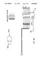
- FIG. 1shows a block diagram of a video display adjustment and on-screen menu system in accordance with the present invention.
- FIGS. 2A-2Hshow a circuit diagram of a video display adjustment and on-screen menu system in accordance with the present invention.
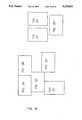
- FIGS. 3A-3Ba circuit diagram of an analog switch and associated sample and hold circuits.
- FIGS. 4A-4Eshow a circuit diagram of several analog switches and associated sample and hold circuits.
- FIG. 5shows a flow chart of the operation of the present invention.
- FIG. 1shows a schematic diagram of the video display adjustment and on-screen menu system 10 in accordance with the present invention.
- the system 10comprises three principle functional blocks: an input, memory storage and controller block 12, a video display adjustment block 14 and a character display block 16.
- an input, memory storage and controller block 12either a front panel 18 or a PC connector 20 can be used to input adjustment selections to the system 10.
- These inputsare temporarily buffered in an input latch 22.
- a microcontroller 24accepts these inputs from the input latch 22, and stores changes to the video display parameters in an EEPROM memory storage area 25.
- certain display parameters provided by the microcontrollerare buffered by an output latch 26.
- the majority of the display parametersare sequentially sent to a DAC 28 that converts the parameters to analog signals.
- These analog signalsare demultiplexed by a series of analog switches 30 enabled after every vertical sync pulse.
- the signals of each switch 30are stored by a complementary series of sample-and-hold circuits 32. These circuits hold the parameters for display operation until new parameters are provided.
- the third block, the character display block 16,generates and sends on-screen menu information to the video display synchronized to the display's horizontal frequency.
- the column counters 34increment for each pixel being sent divided by the number of pixels per character. In the preferred embodiment, each character is 8 pixels across, so the column counters 34 divide the video clock signal by eight. When the column counters 34 reach their end, the current line of the menu has been reached.
- a character size control block 36decides whether to repeat the current pixel Ene (essentially elongating a character). Because higher horizontal frequencies indicate an increased vertical resolution of the display screen, repeating individual character lines increases their vertical size. Characters in the preferred embodiment are created on an 8 by 8 grid, and then each pixel line is doubled, to create an 8 by 16 displayed character.
- each pixel line of a characteris doubled once more to create an 8 by 32 displayed character.
- the character size control blockallows the row counters 38 to increment to the next pixel line of the characters in the menu.
- a display memory 40holds the current array of character codes that make up the displayed menu. Every eight video clock ticks, the column counter 34 increments to indicate the next character code in the current menu line. Every 16 (or if doubled, 32) horizontal sync pulses (scan lines), the row counters 38 increment the display memory 40 to the next full line of character codes in the current menu.
- the current character code (in ASCII) pointed to in the display memory 40 by the column and row counters 34 and 38refers to character display information stored in a character PROM memory 42. Every horizontal sync pulse, the row counters 34 indicate which pixel line of the current character display information is read out of the character PROM 42. These pixel lines are repeated 2 or 4 times depending on the horizontal frequency, as described.
- the pixel line for each character in the current embodimentis 8 pixels wide and is stored in a shift register 46, where it is clocked out to a video drive 48.
- the video drive 48blanks the current space on the video screen and replaces the video display with the current pixel line of character display information.
- a video clock 44provides the appropriate video clock information to the column counters 34, the row counters 38 and the shift register 46 for synchronizing the output of each pixel of menu information.
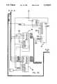
- FIGS. 2, 3 and 4present circuit schematics of the present invention that describe its construction and operation in greater detail.
- FIG. 2reveals most of the video display adjustment and on-screen menu system 10.
- the front panel 18 in the preferred embodimentcomprises a series of switches having outputs labeled Reset, Up, Down and Select. Reset resets all user adjustments to factory preset conditions, Select selects adjustments from the on-screen menu, Up increments an adjustment, and Down decrements an adjustment.
- These switch-provided inputscan be complemented by a series of direct inputs from a PC connector 20, allowing direct input to the menu system from an automated factory adjustment system.
- the inputsare buffered by an input latch 22, comprising a 74LS373 octal transparent latch with 3-state outputs.
- the microcontroller 24reads information from the input latch through its ports P0.1 through P0.7 whenever LAT1 is enabled.
- the horizontal sync (HS) and vertical sync (VS) signalsare also sent through the input latch 22 to the microcontroller 24, which determines whether they are present and their polarities. If HS and VS are not present then either SOG or a composite sync signal is used.
- the HS signalis sent to the INTO port of microcontroller 24 since its pulse width can be too small to be detected by the microcontroller 24 otherwise.
- the monitorcan receive sync information in three ways: (a) separate horizontal and vertical sync signals; (b) a composite sync signal (where the horizontal and vertical sync are added together into one sync signal); and (c) a Sync On Green (SOG) signal, where the composite sync signal is added to the GREEN signal.
- the microcontroller 24determines which of the three types of sync signal is being sent, then generates the SOG and CMPS signal to let the corresponding circuits know what is being sent.
- the microcontroller 24preferably employs a 80C51 CMOS 8-bit CPU and a 16 MHz oscillator. In addition to controlling the on-screen menu system and the CRT display parameters, the microcontroller 24 creates the pin-cushion correction waveform for the display. A 16 MHz oscillator was chosen to provide the necessary bandwidth to synthesize the waveform.
- the signals used throughout the invention as inputs and outputs of the microcontroller 24have the following meanings: INTO is an external interrupt activated by a high-to-low transition of the vertical sync signal, that lets the microcontroller 24 know when to start generating the pin-cushion signal. Therefore, the preferred embodiment uses a negative vertical sync signal.
- the DUO inputis also used to determine if the monitor is running synchronization on green and the horizontal sync HS. This alterative procedure occurs when the input latch 22 is enabled and the HS signal passes through to INTO.
- An inverter 49is used to invert the VS signal and provide an open collector output to share with the input latch's HS output.
- the inverted signals HS' and VSIare always positive going horizontal and vertical synchronization pulses.
- INT1provides an output signal WEEP* that is the chip enable command for the EEPROM memory 25 when reading and writing to the EEPROM 25.
- the T0 inputreceives the HS' signal, allowing the microcontroller 24 to count the number of scan lines. The number of lines is used by the pin generation algorithm, and also to look up appropriate display parameters for a new horizontal frequency and then output these new parameters to the display.
- T1provides the CRID output signal that is logical 1 when the on-screen menu is enabled.
- Port P1.0-7is an eight-bit data port that outputs the display parameter signals (including the pin-cushion waveform) to the DAC 28.
- the RXD pinoutputs a CLRL signal that clears the row counters 38.
- This methodis used for ease of programming and speed. There are only two dead periods during the display tracing where the pin-cushion waveform is not generated: during vertical retrace and in the center of the display. Two separate displays are shown during the on-menu operations of the present invention: a main menu, and a smaller Value Indicator Graph (VIG) that graphically represents the increments and decrements made by a user to a given display parameter (such as brightness). There is enough time in the center of the trace to allow the VIG to be erased and re-written to the screen while keeping the display steady. When the main menu is being displayed, however, there is not enough time even during the center portion of the trace. Therefore, the present invention rewrites the main menu in two complete trace cycles. First the menu is cleared from the SRAM display memory area 40 in one cycle, and then is written in the next cycle, when the row counters 38 are also cleared.
- VOGValue Indic
- the TXD pinoutputs the WRAM* signal which is the SRAM write enable signal, for writing to the display memory 40.
- the ALE pinoutputs the Address Latch Enable (ALE) signal which is the general read/write enable signal generated by the microcontroller 24 for reading and writing all external RAM and ROM memories (such as EEPROM 25 and display memory 40).
- ALEAddress Latch Enable
- the WR* signalis the write enable command generated by the microcontroller 24 for writing to external RAM and ROM memories, while the RD* signal is the read enable command for reading these external memories.
- LATOis used to control the output latch 26
- LAT1is used to control the input latch 22.
- ASO*, AS1* and AS2*enable analog switches 0, 1 and 2 respectively (analog switches 30A, B and C).
- the rest of port P2 (P2.0 through P2.2) along with port P0 (P0.0 through P0.7)provides an 11-bit data and address bus DB0-10 for accessing external RAM and ROM through the invention.
- DB0-5connect to the output latch 26 comprising a 74LS174 hex D Flip-Flop integrated circuit.
- Output latch 26stores several of the display parameters that are changed whenever a new video mode is present.
- the stored parameters of the output latchare changed by enabling LATO upon recognizing the new video mode, latching the outputs of P0.0-5 (via DB0-5) to the outputs of the output latch.
- the CMPS signalis 1 if no VS signal is present, indicating a composite video signal.
- the SLO signalcontrols the size of the characters displayed. If SLO equals 0, each character has an 8 by 16 cell. If SLO equals 1, the cell is 8 by 32. The SLO signal is sent to the character size control block 36 discussed further below.
- Signals SC0-2comprise a 3-bit signal indicating the horizontal frequency. If the signals SC0-2 equal 7, the frequency is 30 khz, if the signals SC0-2 equal 0, the frequency is 75 khz. All other values proportionately divide up the frequency spectrum between these two extremes. The SC0-2 values can then be used to switch in S capacitors for different frequencies to keep acceptable horizontal linearity of the display. The use of S capacitors for this purpose is well known to those skilled in the art.
- the EEPROM chip 25 used in the preferred embodimentis an XL2816AP-250 that is rated for a minimum of 10,000 writes per byte of memory.
- the EEPROM 25stores all the video display adjustment settings. -
- the chip select read enable (RD*) and write enable (WR*)are controlled by the microcontroller 24 as discussed above.
- the EEPROM chip 25 outputs DO-7are sent to the P0 port of the microcontroller 24.
- the address lines for the EEPROM chip 25come from the column and row counter outputs COL 0 through COL 4 and ROW 0 through ROW 5.
- the present inventionuses the column and row counters 34 and 38 also as address latches for addressing the EEPROM 25.
- the particular chips chosen for the column and row counters 34, 38are presettable, allowing them to function as these latches.
- DB0-10loads the EEPROM read/write address into the column and row counters 34 and 38, enabled by the ALE signal. Then, the counters' outputs address the appropriate byte of EEPROM memory while DB0-7 reads or writes that byte's data.
- the digital-to-analog (DAC) block 28receives its 8-bit digital signal from port P1 of microcontroller 24, and converts the signal to analog form to provide to the analog switches 30 and their respective sample-and-hold circuits 32.
- the DAC 28provides a ⁇ 1% linearity with a linear change in digital input. While the schematic of FIG. 2 illustrates the DAC 28 comprising discrete components, an appropriate integrated DAC can be substituted.
- An 74LS05 hex inverter ICprovides an open collector hex inverter since the P1 outputs of the microcontroller 24 are not truly open collector and can cause non-linearities. The specifications of the particular components are as shown in FIG. 2.
- the output VADJ of the DAC 28connects with three analog switches 30.
- each analog switch 30comprise a CD4051B single 8 channel analog multiplexer.
- the single DAC output VADJdrives the three separate analog switches 30 to provide 24 separate adjustments.
- Each respective analog switch 30A, B and Cis switched to on via signals AS0-2.
- Data bus lines DB8-10then select 1 of 8 output lines of the analog switch to enable.
- all 24 adjustmentsare updated by sequentially turning on each analog switch and then, in turn, that switch's separate output lines S0-7, T0-7 and U0-7.
- Each circuitreceives one line from a given analog switch 30.
- switch 32greceives signal S6 from analog switch 30a. The signal S6 is turned on when ASO* is high, and DB8-10 reads "110".
- Switch 32gthe Focus adjustment for the display. All the switch outputs, connection and truth tables are provided below in Table 1.
- Each sample-and-hold (S/H) circuit 32comprises an LM358 low-power op amp.
- the capacitors chosen for the S/H circuits 32are 0.033 ⁇ farads.
- Each S/H circuit 32is updated for 6 ⁇ secs. every vertical sync pulse.
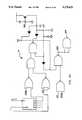
- the character display block 16provides the on-screen menus and value indicator graphs for changing the display parameters.
- the display of the menusis regulated by the column and row counters 34 and 38.
- Column counters 34preferably comprise chained 74F161 synchronous presettable binary counters.
- the first three output lines AD0-2clock the eight pixels of each character pixel line and latch data from the character PROM 42 to the Shift Register 46.
- the higher-level signal lines COL0-COL4address the display memory 40, indicating which character on the current menu line is active.
- the final output, RCOindicates that the 32 columns of the menu line have been completed, and temporarily stops the video oscillator clock 44, until the next horizontal sync signal HS activates the clock again.
- the CLK signal for the countersis generated by the video oscillator clock 44.
- the column and row counters 34 and 38double as address latches for reading and writing the EEPROM 25.
- the ALE signalis substituted for the CLK signal.
- the row counters 38are also formed from chained 74LS161 synchronous presettable binary counters.
- the first 2 outputs of the row counters LNE1-2are sent to the character PROM's second and third input bits, since each character has eight lines and each line is at least doubled (and sometimes quadrupled).
- LNE0(which attaches to the character PROM's first input, comes directly from the character size control block 36, discussed further below.
- the remaining output signals ROW0-5address the display memory block 40, determining which row of character to display. Again, since the counters double as address latches for reading and writing the EEPROM 25, the data is latched using ALE instead of the CLK signal.
- the character size control block 36sits functionally between the column counters 34 and the row counters 38. During menu display, as the columns for a given row (of character pixel line information) are exhausted, the character size control block determines whether to advance the row counters to the next row. In lower horizontal frequencies, each line of a character is doubled: i.e., the column counters cycle through two complete cycles of the same character line before advancing the row counters. At higher frequencies, when characters would appear squashed, the character size control block 36 retards the row counter advance for four complete column cycles. The character size control block 36 counts horizontal rows by using the HC* signal from the column counter block 34, which is the same as the horizontal sync signal HS.
- the character size control block 36preferably comprises a 74LS393 dual 4 stage binary counter and a 74LS151 8 input multiplexer, as indicated in FIG. 2.
- the ALE signalis substituted as the row clock so that address lines can be latched into the row counters 38 (when they function as address latches).
- the LCL signal lineis the clock line for the row counters. Again, the CLRL signal from the microcontroller 24 clears the counters during the Vertical Retrace, while the CRID* signal is the CRT display enable signal.
- Table 2provides the relation between these signals.
- the addresses generated by the column and row counters 34 and 38are sent to the display memory block 40, comprising 2 1K by 4 static RAM 2114Al-2 chips.
- ROW0-4are the row address lines, allowing 32 possible menu rows to be stored
- COL--4are the column address lines, allowing 32 characters per row.
- DB0-7are the data input lines from the microcontroller 24 that can store characters for each address location.
- Outputs DB0-5connect to the character PROIF 42 to indicate which character to display, while outputs DB6-7 connect to the video drive 48 to cause appropriate video blanking and color for the menu.
- the WRAM* signalis the write enable for the display meniory SRAMS, and the microcontroller VrR* signal connects to each chip's CS* pin.
- the VFEEP* signalis 0 if writing to the EEPROM 25, such that no writing is done to the display memory 40.
- the systemis capable of displaying 32 rows, a maximum of 16 rows can be displayed before the VS signal clears the counter. To assure that the display is always in the horizontal active area, only columns 8 through 24 are used. Also, due to speed limitations of the microcontroller 24, only 5 rows are used.
- the character PROM memory block 42comprises a 74S472 512-by-8 byte TIL PROM.
- Signals LN0-2comprise the 3-bit character line address (providing 8 lines per character) that comes from the row counters 38.
- Signals DB0-5comprise the 6 bit character address (allowing 64 possible characters) from the display memory block 40.
- Data lines 01-8provide the character pixel line information (having 8 pixels per character line) latched from the character PROM memory block 42 to the shift register block 46 for output to the video display.
- DB0-5determine which character to display, while LN0-2 determine which line of that character to output.
- the character PROM 42outputs the 8 pixels of the current pixel line of the current character.
- the video clock 44provides the coordinating timing mechanism for the character display section 16.
- the clock 44is a variable oscillator that is synchronized to the incoming horizontal frequency.
- the clock's frequencyis controlled by varying an OSV voltage (determined by microcontroller 24 and stored by S/H circuit 32e) such that character size is kept fairly constant, regardless of horizontal frequency.
- the oscillatoris kept synchronous to the horizontal frequency to maintain the menu information stationary on the video display.
- the video clock frequencyis varied by controlling the Constant current source to the oscillator by varying OSV.
- the clockis synchronized to the horizontal frequency by gating the horizontal sync signal HS with the oscillator, starting the oscillator when each horizontal line occurs.
- the clockis turned off when the columns for the display complete their cycle for one line.
- the OSV signalis an analog 10-15 V signal stored by S/H circuit 32e.
- RCO from counter U10goes high when the counters reach FF (their end) and lulls the video clock by using a 74LS393 as a latch.
- the horizontal sync signal HS'restarts the clock by clearing this 74LS393 latch.
- the output CLKdrives the counters 34 and 38, while the inverse output CLK* drives shift register 46. Table 3 presents a truth table relating these signals.
- the video clock 44uses a 74F132 quad 2 input NAND Schmitt trigger, a 74LS02 Quad 2 input NOR gate, and other discrete components as indicated.
- the clock outputis between 10 and 20 Mhz dependent on incoming horizontal frequency.
- the clock's frequencypreferably defaults to be proportional to the horizontal frequency.
- the usercan also adjust the oscillator frequency for each mode by making selections on the menu, thereby controlling the horizontal size of the characters.
- the shift register 46is a 74F166 8 bit shift parallel-to-serial register. Data lines 01-8 from the character PROM 42 provide the video information to the shift register (the current pixel line for the current character).
- the CLK* signal from the video clock 44shifts the data to the output one bit at a time.
- AD0-2are from the column counters 34 that latches a new set of pixel information every 8 video clock ticks, loading the next character's pixel line.
- Zis the video signal output sent to the video drive 48.
- the video drive block 48drives transistor amplifiers on the video display's driver circuitry.
- the video information normally sent to the video displayis blanked for an entire character whenever character information is written to the display during menu operation. AU other times, the normal video information is sent to the video display.
- the video drive block 48employs three 74LS08 Quad 2 input AND gates.
- the Z lineis the video signal from the shift register, signal DB6 allows the Z signal to also drive the blue video signal, and signal DB7 is from the display memory block and blanks the PC's video for 1 character cell.
- the CRTD* signalis used to avoid false triggers: the system only blanks a character cell when this signal is active.
- RGDis the video signal drive for the red and green video signals.
- BDis the blue video signal, and BLANK blanks the RGB video signal sent from the computer that normally drives the display.
- the sequential operation of the present inventionis described in flow chart 50 of FIG. 5.
- the initial conditions for the displayare read 52 by the microcontroller 24 from the EEPROM memory 25 and sent via the DAC 28 and digital switches 30 to the individual sample-and-hold circuits 32.
- the microcontroller 24counts the number of horizontal lines traced and determines 54 if the number of lines differ from the previous count. If not, the microcontroller asks 56 whether the user has started to make any adjustments. If that is also not true, the microcontroller determines 58 if the reset button on the front panel 18 has been pressed. If the answer is also false, the microcontroller begins generating the top of the pincushion waveform 60. If any menu is being displayed, its contents are written 62 at the middle of the display trace to the display memory block 40. Then the microcontroller 24 generates the bottom of the pincushion waveform 64.
- the microcontroller 24updates all S/H circuits 32, clears the menu display and counters 34, 38 and 40, and counts the number of horizontal lines again. If the line count is different, a different horizontal frequency is being used. The microcontroller 24 then determines 68 the horizontal frequency, the vertical frequency and the polarities of the signals. Having determined which new frequency mode is being used, the menu system then reads the appropriate display parameters 70 from the EEPROM memory 25. These display parameters are then converted and sent 72 to the S/H circuits 32, and the microcontroller 24 begins the normal operation of generating the pincushion waveform in steps 60 through 66.
- the microcontroller 24changes the appropriate adjustment value, both in the EEPROM memory 25, and at the next vertical retrace 66, the appropriate S/H circuit 32. If the user presses the Reset button at step 58, the microcontroller 24 reads 74 the appropriate EEPROM memory for the factory-default standards for the current frequency mode. Meanwhile, the nominal operation of generating the pincushion waveform, displaying the menu display, and updating the S/H circuits 32 at the vertical sync signal occur as before in steps 60 through 66.
Landscapes
- Engineering & Computer Science (AREA)
- Physics & Mathematics (AREA)
- Computer Hardware Design (AREA)
- General Physics & Mathematics (AREA)
- Theoretical Computer Science (AREA)
- Radar, Positioning & Navigation (AREA)
- Remote Sensing (AREA)
- Controls And Circuits For Display Device (AREA)
- Transforming Electric Information Into Light Information (AREA)
- Television Receiver Circuits (AREA)
Abstract
Description
TABLE 1 __________________________________________________________________________Switch Adjustment Input AS0* AS1* AS2* DB8 DB9 DB10 __________________________________________________________________________32a HPOS S0 1 0 0 0 0 032b HSIZE S1 1 0 0 0 0 132c VSIZE S2 1 0 0 0 1 032d VPOS S3 1 0 0 0 1 132e OSV S4 1 0 0 1 0 032f HSIZE S5 1 0 0 1 0 132g FOCUS S6 1 0 0 1 1 032h G2 S7 1 0 0 1 1 1 32i n/aT0 0 1 0 0 0 032j PWR T1 0 1 0 0 0 132k NV T2 0 1 0 0 1 032l DYNFOC T3 0 1 0 0 1 132m HHLD T4 0 1 0 1 0 032n HCTR T5 0 1 0 1 0 132o VHLD T6 0 1 0 1 1 032p VLIN T7 0 1 0 1 1 132q RBIAS U0 0 0 1 0 0 032r RGAIN U1 0 0 1 0 0 132s GBIAS U2 0 0 1 0 1 032t GGAIN U3 0 0 1 0 1 132u BBIAS U4 0 0 1 1 0 032v BGAIN U5 0 0 1 1 0 132w CONTRAST U6 0 0 1 1 1 032x BRIGHT U7 0 0 1 1 1 1 __________________________________________________________________________
TABLE 2 ______________________________________ CLRL SL0 CRTD* LCL ______________________________________ 1X 0 0X X 1ALE 0 0 0 HS/2 0 1 0 HS/4 ______________________________________
TABLE 3 ______________________________________ CRTD* HS' RCO CLK* ______________________________________ 1X X ALE 0 1X 0 0 0 0Video Clock 0 0 1 0 ______________________________________
Claims (16)
Priority Applications (11)
| Application Number | Priority Date | Filing Date | Title |
|---|---|---|---|
| US07/796,411US5270821A (en) | 1991-11-22 | 1991-11-22 | Video display adjustment and on-screen menu system |
| CA002060396ACA2060396C (en) | 1991-11-22 | 1992-01-30 | Video display adjustment and on-screen menu system |
| MYPI92000303AMY109650A (en) | 1991-11-22 | 1992-02-25 | Video display adjustment and on-screen menu system |
| KR1019920008550AKR0160277B1 (en) | 1991-11-22 | 1992-05-20 | The video display adjustment and on-screen menu system |
| EP92113837AEP0543089B2 (en) | 1991-11-22 | 1992-08-13 | Video display adjustment and on-screen menu system |
| SG1996008233ASG52717A1 (en) | 1991-11-22 | 1992-08-13 | Video display adjustment and on-screen menu system |
| EP97106525AEP0817158B1 (en) | 1991-11-22 | 1992-08-13 | Video display adjustment and on-screen menu system |
| DE69233728TDE69233728T2 (en) | 1991-11-22 | 1992-08-13 | Video display setup and menu system on screen |
| DE69225777TDE69225777T3 (en) | 1991-11-22 | 1992-08-13 | Video display setup and menu system on screen |
| JP04285872AJP3079173B2 (en) | 1991-11-22 | 1992-10-23 | Video display adjustment and menu system on display screen |
| MX9206666AMX9206666A (en) | 1991-11-22 | 1992-11-19 | ADJUSTMENT FOR VIDEO DISPLAY AND ON-SCREEN MENU SYSTEM. |
Applications Claiming Priority (1)
| Application Number | Priority Date | Filing Date | Title |
|---|---|---|---|
| US07/796,411US5270821A (en) | 1991-11-22 | 1991-11-22 | Video display adjustment and on-screen menu system |
Publications (1)
| Publication Number | Publication Date |
|---|---|
| US5270821Atrue US5270821A (en) | 1993-12-14 |
Family
ID=25168134
Family Applications (1)
| Application Number | Title | Priority Date | Filing Date |
|---|---|---|---|
| US07/796,411Expired - LifetimeUS5270821A (en) | 1991-11-22 | 1991-11-22 | Video display adjustment and on-screen menu system |
Country Status (9)
| Country | Link |
|---|---|
| US (1) | US5270821A (en) |
| EP (2) | EP0543089B2 (en) |
| JP (1) | JP3079173B2 (en) |
| KR (1) | KR0160277B1 (en) |
| CA (1) | CA2060396C (en) |
| DE (2) | DE69225777T3 (en) |
| MX (1) | MX9206666A (en) |
| MY (1) | MY109650A (en) |
| SG (1) | SG52717A1 (en) |
Cited By (35)
| Publication number | Priority date | Publication date | Assignee | Title |
|---|---|---|---|---|
| US5457473A (en)* | 1992-02-20 | 1995-10-10 | Hitachi, Ltd. | Image display apparatus |
| US5483260A (en)* | 1993-09-10 | 1996-01-09 | Dell Usa, L.P. | Method and apparatus for simplified video monitor control |
| US5485278A (en)* | 1990-08-29 | 1996-01-16 | Canon Kabushiki Kaisha | Character processing method and apparatus with brightness correction based output size |
| US5644757A (en)* | 1995-06-12 | 1997-07-01 | United Microelectronics Corporation | Apparatus for storing data into a digital-to-analog converter built-in to a microcontroller |
| US5748251A (en)* | 1994-01-14 | 1998-05-05 | Funai Electric Co., Ltd. | Apparatus with a built-in teletext broadcasting decoder and teletext display adjustment apparatus |
| US5808693A (en)* | 1995-11-07 | 1998-09-15 | Sony Corporation | Video display apparatus with power saving modes |
| US5828351A (en)* | 1997-01-16 | 1998-10-27 | Acer Peripherals, Inc. | Method and apparatus of adjusting monitor display |
| US5877745A (en)* | 1994-07-15 | 1999-03-02 | International Business Machines Corporation | Data processing system having a wireless communication link for data communication with a peripheral device |
| US5912663A (en)* | 1996-07-09 | 1999-06-15 | Mag Technology, Co., Ltd. | Monitor adjustments made by a single rotatable and depressible knob which interfaces with a monitor control display menu |
| US5917468A (en)* | 1996-01-15 | 1999-06-29 | Lg Electronics Inc. | Apparatus for controlling an operation of a display data channel in a monitor and a method thereof |
| US5936680A (en)* | 1996-02-20 | 1999-08-10 | Kabushiki Kaisha Toshiba | Multimedia television receiver |
| US6008836A (en)* | 1996-06-03 | 1999-12-28 | Webtv Networks, Inc. | Method and apparatus for adjusting television display control using a browser |
| US6134606A (en)* | 1997-07-25 | 2000-10-17 | Flashpoint Technology, Inc. | System/method for controlling parameters in hand-held digital camera with selectable parameter scripts, and with command for retrieving camera capabilities and associated permissible parameter values |
| US6169535B1 (en) | 1997-06-30 | 2001-01-02 | Toshiba America Information Systems, Inc. | Monitor adjustment control |
| US6208326B1 (en)* | 1997-09-30 | 2001-03-27 | Compaq Computer Corporation | Apparatus and associated method for selecting video display parameter of a computer-system, video display monitor |
| US6369810B1 (en)* | 1997-07-25 | 2002-04-09 | U.S. Philips Corporation | Digital monitor |
| US6400377B1 (en)* | 1995-11-24 | 2002-06-04 | Nanao Corporation | Video monitor adjustment system |
| US6513088B2 (en) | 1993-02-10 | 2003-01-28 | Hitachi, Ltd. | Display unit and method enabling bi-directional communication with video source |
| US6714190B2 (en)* | 1999-02-26 | 2004-03-30 | Canon Kabushiki Kaisha | Image display control method and apparatus, and display apparatus |
| US6891633B1 (en)* | 1999-07-30 | 2005-05-10 | Xerox Corporation | Image transfer system |
| US6950097B1 (en)* | 2002-12-02 | 2005-09-27 | National Semiconductor Corporation | Video display interface controller for host video display unit |
| US20050270421A1 (en)* | 2004-06-02 | 2005-12-08 | Mstar Semiconductor, Inc. | Method and device for dynamically adjusting sync-on-green (SOG) signal of video signal |
| US6982695B1 (en)* | 1999-04-22 | 2006-01-03 | Palmsource, Inc. | Method and apparatus for software control of viewing parameters |
| WO2007123573A1 (en)* | 2006-04-24 | 2007-11-01 | Thomson Licensing | Method and apparatus for providing an on-screen menu system |
| US20110010632A1 (en)* | 1995-08-25 | 2011-01-13 | Beasley Danny L | Computer interconnection system |
| US20110022988A1 (en)* | 2009-07-27 | 2011-01-27 | Lg Electronics Inc. | Providing user interface for three-dimensional display device |
| US20110080381A1 (en)* | 2009-10-06 | 2011-04-07 | Mstar Semiconductor, Inc. | Portable Control Apparatus and Method Thereof |
| US20110126160A1 (en)* | 2009-11-23 | 2011-05-26 | Samsung Electronics Co., Ltd. | Method of providing 3d image and 3d display apparatus using the same |
| US8102457B1 (en) | 1997-07-09 | 2012-01-24 | Flashpoint Technology, Inc. | Method and apparatus for correcting aspect ratio in a camera graphical user interface |
| US8127232B2 (en) | 1998-12-31 | 2012-02-28 | Flashpoint Technology, Inc. | Method and apparatus for editing heterogeneous media objects in a digital imaging device |
| CN103110428A (en)* | 2011-11-16 | 2013-05-22 | 深圳迈瑞生物医疗电子股份有限公司 | Ultrasonic imaging method and system |
| USRE44814E1 (en) | 1992-10-23 | 2014-03-18 | Avocent Huntsville Corporation | System and method for remote monitoring and operation of personal computers |
| US9224145B1 (en) | 2006-08-30 | 2015-12-29 | Qurio Holdings, Inc. | Venue based digital rights using capture device with digital watermarking capability |
| US10388054B2 (en) | 2016-06-03 | 2019-08-20 | Apple Inc. | Controlling display performance using animation based refresh rates |
| US10510317B2 (en) | 2016-06-03 | 2019-12-17 | Apple Inc. | Controlling display performance with target presentation times |
Families Citing this family (8)
| Publication number | Priority date | Publication date | Assignee | Title |
|---|---|---|---|---|
| JP3971465B2 (en)† | 1995-06-08 | 2007-09-05 | ソニー株式会社 | Camera setup method and system |
| JP3525589B2 (en)* | 1995-11-06 | 2004-05-10 | ソニー株式会社 | Image display device and image display method |
| JPH09135403A (en)* | 1995-11-09 | 1997-05-20 | Sony Corp | Image display device |
| US5948091A (en)* | 1995-12-01 | 1999-09-07 | Texas Instruments Incorporated | Universal digital display interface |
| DE19616624A1 (en) | 1996-04-25 | 1997-11-06 | Thomas Mohr | Screen display method and screen display device and apparatus herewith |
| US7707613B1 (en) | 1998-01-05 | 2010-04-27 | Gateway, Inc. | Individualized parameter control for multiple media sources in a data processing system |
| KR100766970B1 (en) | 2001-05-11 | 2007-10-15 | 삼성전자주식회사 | Initial setting system of display device and its control method |
| US6930655B2 (en)* | 2001-07-31 | 2005-08-16 | Koninklijke Philips Electronics N.V. | Display monitor has stand-alone mode and PC peripheral mode |
Citations (8)
| Publication number | Priority date | Publication date | Assignee | Title |
|---|---|---|---|---|
| US4024531A (en)* | 1974-03-05 | 1977-05-17 | National Research Development Corporation | Display devices |
| US4405836A (en)* | 1982-01-04 | 1983-09-20 | Motorola, Inc. | Signal equalization selector |
| US4495652A (en)* | 1983-02-28 | 1985-01-22 | General Electric Company | Control arrangement for radio apparatus |
| US4710800A (en)* | 1984-04-27 | 1987-12-01 | Utah Scientific Advanced Development Center, Inc. | Apparatus for allowing operator selection of a color region of a video image for receiving color corrections |
| US4755955A (en)* | 1983-07-06 | 1988-07-05 | Kabushiki Kaisha Toshiba | Document creating apparatus |
| US4837627A (en)* | 1987-08-19 | 1989-06-06 | Rca Licensing Corporation | Programmable operating-parameter control appatatus for a television receiver |
| US5005084A (en)* | 1989-12-19 | 1991-04-02 | North American Philips Corporation | Remote control television system using supplementary unit for simplified personalized control |
| US5051827A (en)* | 1990-01-29 | 1991-09-24 | The Grass Valley Group, Inc. | Television signal encoder/decoder configuration control |
Family Cites Families (20)
| Publication number | Priority date | Publication date | Assignee | Title |
|---|---|---|---|---|
| IT1159686B (en)† | 1978-05-22 | 1987-03-04 | Indesit | TELEVISION |
| IT1108410B (en)† | 1978-09-25 | 1985-12-09 | Indesit | TELEVISION |
| EP0057314B1 (en)* | 1981-01-28 | 1985-12-04 | BURROUGHS CORPORATION (a Delaware corporation) | Lsi timing circuit for a digital display employing a modulo eight counter |
| GB2145909B (en)* | 1983-09-01 | 1987-05-13 | Philips Electronic Associated | A double height algorithm for crt character display |
| US4626892A (en)* | 1984-03-05 | 1986-12-02 | Rca Corporation | Television system with menu like function control selection |
| JPS61103358A (en)* | 1984-10-26 | 1986-05-21 | Ricoh Co Ltd | n double-width character generation method |
| JPS6390372A (en)† | 1986-09-30 | 1988-04-21 | Toyota Motor Corp | Panel member for weld bolt deposition |
| JPS6357697U (en)* | 1986-09-30 | 1988-04-18 | ||
| DE3722169C2 (en)* | 1987-07-04 | 1997-06-05 | Thomson Brandt Gmbh | Method and device for carrying out the method for adapting a multi-mode monitor to a personal computer |
| JPH0227190U (en)* | 1988-03-14 | 1990-02-22 | ||
| US4907082A (en)† | 1988-05-03 | 1990-03-06 | Thomson Consumer Electronics, Inc. | Dynamic control menu for a television system or the like |
| JPH01314291A (en)* | 1988-06-15 | 1989-12-19 | Hitachi Ltd | Display device adaptive to multiple frequencies with function to store adjustment data of display screen |
| JP2535395B2 (en)† | 1988-12-23 | 1996-09-18 | 株式会社日立製作所 | Image display device |
| JP2726305B2 (en)† | 1989-04-17 | 1998-03-11 | 株式会社日立製作所 | Image display device |
| US4962428A (en)† | 1989-04-20 | 1990-10-09 | Motorola, Inc. | Multistandard OSD in a TV receiver including display positioning |
| US4953027A (en)* | 1989-04-24 | 1990-08-28 | Motorola Inc. | OSD in a TV receiver including a window, smoothing and edge enhancing |
| US4991023A (en)* | 1989-05-22 | 1991-02-05 | Hewlett-Packard Company | Microprocessor controlled universal video monitor |
| JPH02312368A (en)* | 1989-05-26 | 1990-12-27 | Sony Corp | Television receiver |
| JPH02312464A (en)* | 1989-05-29 | 1990-12-27 | Mitsubishi Electric Corp | on-screen display device |
| JPH0352790U (en)† | 1989-09-29 | 1991-05-22 |
- 1991
- 1991-11-22USUS07/796,411patent/US5270821A/ennot_activeExpired - Lifetime
- 1992
- 1992-01-30CACA002060396Apatent/CA2060396C/ennot_activeExpired - Lifetime
- 1992-02-25MYMYPI92000303Apatent/MY109650A/enunknown
- 1992-05-20KRKR1019920008550Apatent/KR0160277B1/ennot_activeExpired - Fee Related
- 1992-08-13EPEP92113837Apatent/EP0543089B2/ennot_activeExpired - Lifetime
- 1992-08-13DEDE69225777Tpatent/DE69225777T3/ennot_activeExpired - Lifetime
- 1992-08-13SGSG1996008233Apatent/SG52717A1/enunknown
- 1992-08-13DEDE69233728Tpatent/DE69233728T2/ennot_activeExpired - Lifetime
- 1992-08-13EPEP97106525Apatent/EP0817158B1/ennot_activeExpired - Lifetime
- 1992-10-23JPJP04285872Apatent/JP3079173B2/ennot_activeExpired - Lifetime
- 1992-11-19MXMX9206666Apatent/MX9206666A/enunknown
Patent Citations (8)
| Publication number | Priority date | Publication date | Assignee | Title |
|---|---|---|---|---|
| US4024531A (en)* | 1974-03-05 | 1977-05-17 | National Research Development Corporation | Display devices |
| US4405836A (en)* | 1982-01-04 | 1983-09-20 | Motorola, Inc. | Signal equalization selector |
| US4495652A (en)* | 1983-02-28 | 1985-01-22 | General Electric Company | Control arrangement for radio apparatus |
| US4755955A (en)* | 1983-07-06 | 1988-07-05 | Kabushiki Kaisha Toshiba | Document creating apparatus |
| US4710800A (en)* | 1984-04-27 | 1987-12-01 | Utah Scientific Advanced Development Center, Inc. | Apparatus for allowing operator selection of a color region of a video image for receiving color corrections |
| US4837627A (en)* | 1987-08-19 | 1989-06-06 | Rca Licensing Corporation | Programmable operating-parameter control appatatus for a television receiver |
| US5005084A (en)* | 1989-12-19 | 1991-04-02 | North American Philips Corporation | Remote control television system using supplementary unit for simplified personalized control |
| US5051827A (en)* | 1990-01-29 | 1991-09-24 | The Grass Valley Group, Inc. | Television signal encoder/decoder configuration control |
Cited By (60)
| Publication number | Priority date | Publication date | Assignee | Title |
|---|---|---|---|---|
| US5485278A (en)* | 1990-08-29 | 1996-01-16 | Canon Kabushiki Kaisha | Character processing method and apparatus with brightness correction based output size |
| US6346930B2 (en) | 1992-02-20 | 2002-02-12 | Hitachi, Ltd. | Computer apparatus for sending video information to an image display apparatus and receiving information from the image display apparatus |
| US6078301A (en)* | 1992-02-20 | 2000-06-20 | Hitachi, Ltd. | Computer apparatus for sending video information to an image display apparatus and receiving information from the image display apparatus |
| US6639588B2 (en) | 1992-02-20 | 2003-10-28 | Hitachi, Ltd. | Image display apparatus |
| US20040196276A1 (en)* | 1992-02-20 | 2004-10-07 | Hitachi, Ltd. | Display unit for displaying an image based on a video signal received from a personal computer which is connected to an input device |
| US6348904B1 (en) | 1992-02-20 | 2002-02-19 | Hitachi, Ltd. | Computer apparatus for sending video information to an image display apparatus and receiving information from the image display apparatus |
| US6686895B2 (en) | 1992-02-20 | 2004-02-03 | Hitachi, Ltd. | Display unit for displaying an image based on a video signal received from a personal computer which is connected to an input device |
| US6057812A (en)* | 1992-02-20 | 2000-05-02 | Hitachi, Ltd. | Image display apparatus which both receives video information and outputs information about itself |
| US5457473A (en)* | 1992-02-20 | 1995-10-10 | Hitachi, Ltd. | Image display apparatus |
| US6304236B1 (en) | 1992-02-20 | 2001-10-16 | Hitachi Ltd. | Display apparatus for adjusting the display image using a control signal from an external computer |
| USRE44814E1 (en) | 1992-10-23 | 2014-03-18 | Avocent Huntsville Corporation | System and method for remote monitoring and operation of personal computers |
| US6513088B2 (en) | 1993-02-10 | 2003-01-28 | Hitachi, Ltd. | Display unit and method enabling bi-directional communication with video source |
| US7475180B2 (en) | 1993-02-10 | 2009-01-06 | Mondis Technology Ltd. | Display unit with communication controller and memory for storing identification number for identifying display unit |
| US7475181B2 (en) | 1993-02-10 | 2009-01-06 | Mondis Technology Ltd. | Display unit with processor and communication controller which communicates information to the processor |
| US7089342B2 (en) | 1993-02-10 | 2006-08-08 | Hitachi, Ltd. | Method enabling display unit to bi-directionally communicate with video source |
| US6549970B2 (en) | 1993-02-10 | 2003-04-15 | Hitachi, Ltd. | Display unit with controller enabling bi-directional communication with computer |
| US5483260A (en)* | 1993-09-10 | 1996-01-09 | Dell Usa, L.P. | Method and apparatus for simplified video monitor control |
| US5748251A (en)* | 1994-01-14 | 1998-05-05 | Funai Electric Co., Ltd. | Apparatus with a built-in teletext broadcasting decoder and teletext display adjustment apparatus |
| US5877745A (en)* | 1994-07-15 | 1999-03-02 | International Business Machines Corporation | Data processing system having a wireless communication link for data communication with a peripheral device |
| US5644757A (en)* | 1995-06-12 | 1997-07-01 | United Microelectronics Corporation | Apparatus for storing data into a digital-to-analog converter built-in to a microcontroller |
| US20110010632A1 (en)* | 1995-08-25 | 2011-01-13 | Beasley Danny L | Computer interconnection system |
| US8443037B2 (en) | 1995-08-25 | 2013-05-14 | Avocent Redmond Corp. | Computer interconnection system |
| US5808693A (en)* | 1995-11-07 | 1998-09-15 | Sony Corporation | Video display apparatus with power saving modes |
| US6400377B1 (en)* | 1995-11-24 | 2002-06-04 | Nanao Corporation | Video monitor adjustment system |
| US5917468A (en)* | 1996-01-15 | 1999-06-29 | Lg Electronics Inc. | Apparatus for controlling an operation of a display data channel in a monitor and a method thereof |
| US5936680A (en)* | 1996-02-20 | 1999-08-10 | Kabushiki Kaisha Toshiba | Multimedia television receiver |
| US6008836A (en)* | 1996-06-03 | 1999-12-28 | Webtv Networks, Inc. | Method and apparatus for adjusting television display control using a browser |
| US5912663A (en)* | 1996-07-09 | 1999-06-15 | Mag Technology, Co., Ltd. | Monitor adjustments made by a single rotatable and depressible knob which interfaces with a monitor control display menu |
| US5828351A (en)* | 1997-01-16 | 1998-10-27 | Acer Peripherals, Inc. | Method and apparatus of adjusting monitor display |
| US6169535B1 (en) | 1997-06-30 | 2001-01-02 | Toshiba America Information Systems, Inc. | Monitor adjustment control |
| US8102457B1 (en) | 1997-07-09 | 2012-01-24 | Flashpoint Technology, Inc. | Method and apparatus for correcting aspect ratio in a camera graphical user interface |
| US8970761B2 (en) | 1997-07-09 | 2015-03-03 | Flashpoint Technology, Inc. | Method and apparatus for correcting aspect ratio in a camera graphical user interface |
| US6369810B1 (en)* | 1997-07-25 | 2002-04-09 | U.S. Philips Corporation | Digital monitor |
| US6812922B2 (en) | 1997-07-25 | 2004-11-02 | Koninklijke Philips Electronics N.V. | Digital monitor |
| US6134606A (en)* | 1997-07-25 | 2000-10-17 | Flashpoint Technology, Inc. | System/method for controlling parameters in hand-held digital camera with selectable parameter scripts, and with command for retrieving camera capabilities and associated permissible parameter values |
| US6208326B1 (en)* | 1997-09-30 | 2001-03-27 | Compaq Computer Corporation | Apparatus and associated method for selecting video display parameter of a computer-system, video display monitor |
| US8127232B2 (en) | 1998-12-31 | 2012-02-28 | Flashpoint Technology, Inc. | Method and apparatus for editing heterogeneous media objects in a digital imaging device |
| US8972867B1 (en) | 1998-12-31 | 2015-03-03 | Flashpoint Technology, Inc. | Method and apparatus for editing heterogeneous media objects in a digital imaging device |
| US6714190B2 (en)* | 1999-02-26 | 2004-03-30 | Canon Kabushiki Kaisha | Image display control method and apparatus, and display apparatus |
| US6982695B1 (en)* | 1999-04-22 | 2006-01-03 | Palmsource, Inc. | Method and apparatus for software control of viewing parameters |
| US6891633B1 (en)* | 1999-07-30 | 2005-05-10 | Xerox Corporation | Image transfer system |
| US6950097B1 (en)* | 2002-12-02 | 2005-09-27 | National Semiconductor Corporation | Video display interface controller for host video display unit |
| US7408592B2 (en)* | 2004-06-02 | 2008-08-05 | Mstar Semiconductor, Inc. | Method and device for dynamically adjusting sync-on-green (SOG) signal of video signal |
| US20050270421A1 (en)* | 2004-06-02 | 2005-12-08 | Mstar Semiconductor, Inc. | Method and device for dynamically adjusting sync-on-green (SOG) signal of video signal |
| CN101427301B (en)* | 2006-04-24 | 2012-09-05 | 汤姆逊许可证公司 | Method and apparatus for providing an on-screen menu system |
| WO2007123573A1 (en)* | 2006-04-24 | 2007-11-01 | Thomson Licensing | Method and apparatus for providing an on-screen menu system |
| US20090158217A1 (en)* | 2006-04-24 | 2009-06-18 | Anthony Edward Stuart | Method and Apparatus for Providing an On-Screen Menu System |
| US9224145B1 (en) | 2006-08-30 | 2015-12-29 | Qurio Holdings, Inc. | Venue based digital rights using capture device with digital watermarking capability |
| US8413073B2 (en)* | 2009-07-27 | 2013-04-02 | Lg Electronics Inc. | Providing user interface for three-dimensional display device |
| US20110022988A1 (en)* | 2009-07-27 | 2011-01-27 | Lg Electronics Inc. | Providing user interface for three-dimensional display device |
| US9093985B2 (en)* | 2009-10-06 | 2015-07-28 | Mstar Semiconductor, Inc. | Portable control apparatus and method thereof for calibrating an oscillating circuit |
| US20110080381A1 (en)* | 2009-10-06 | 2011-04-07 | Mstar Semiconductor, Inc. | Portable Control Apparatus and Method Thereof |
| US20110126160A1 (en)* | 2009-11-23 | 2011-05-26 | Samsung Electronics Co., Ltd. | Method of providing 3d image and 3d display apparatus using the same |
| CN103110428A (en)* | 2011-11-16 | 2013-05-22 | 深圳迈瑞生物医疗电子股份有限公司 | Ultrasonic imaging method and system |
| US10388054B2 (en) | 2016-06-03 | 2019-08-20 | Apple Inc. | Controlling display performance using animation based refresh rates |
| US10510317B2 (en) | 2016-06-03 | 2019-12-17 | Apple Inc. | Controlling display performance with target presentation times |
| US10706604B2 (en) | 2016-06-03 | 2020-07-07 | Apple Inc. | Controlling display performance using display system hints |
| US10726604B2 (en) | 2016-06-03 | 2020-07-28 | Apple Inc. | Controlling display performance using display statistics and feedback |
| AU2020233755B2 (en)* | 2016-06-03 | 2022-05-26 | Apple Inc. | Controlling display performance |
| US11568588B2 (en) | 2016-06-03 | 2023-01-31 | Apple Inc. | Controlling display performance using display statistics and feedback |
Also Published As
| Publication number | Publication date |
|---|---|
| CA2060396C (en) | 2001-04-03 |
| MY109650A (en) | 1997-03-30 |
| EP0817158A2 (en) | 1998-01-07 |
| EP0543089B2 (en) | 2005-08-10 |
| JP3079173B2 (en) | 2000-08-21 |
| KR930010703A (en) | 1993-06-23 |
| JPH05297843A (en) | 1993-11-12 |
| SG52717A1 (en) | 1998-09-28 |
| EP0543089A2 (en) | 1993-05-26 |
| DE69233728D1 (en) | 2008-04-03 |
| DE69225777T2 (en) | 1998-10-01 |
| EP0817158B1 (en) | 2008-02-20 |
| KR0160277B1 (en) | 1999-03-20 |
| MX9206666A (en) | 1993-07-01 |
| DE69225777D1 (en) | 1998-07-09 |
| EP0817158A3 (en) | 1999-07-21 |
| EP0543089A3 (en) | 1994-12-28 |
| CA2060396A1 (en) | 1993-05-23 |
| DE69233728T2 (en) | 2009-02-12 |
| EP0543089B1 (en) | 1998-06-03 |
| DE69225777T3 (en) | 2006-06-22 |
Similar Documents
| Publication | Publication Date | Title |
|---|---|---|
| US5270821A (en) | Video display adjustment and on-screen menu system | |
| US5608423A (en) | Video display processor with pixel by pixel hardware scrolling | |
| US7808448B1 (en) | Raster engine with hardware cursor | |
| US5124804A (en) | Programmable resolution video controller | |
| US5086295A (en) | Apparatus for increasing color and spatial resolutions of a raster graphics system | |
| US7427989B2 (en) | Raster engine with multiple color depth digital display interface | |
| US4683469A (en) | Display terminal having multiple character display formats | |
| JPH04220692A (en) | Display-monitor control system and method thereof | |
| US6831647B1 (en) | Raster engine with bounded video signature analyzer | |
| US6734866B1 (en) | Multiple adapting display interface | |
| KR900005188B1 (en) | Crt controler | |
| US4703322A (en) | Variable loadable character generator | |
| US5376949A (en) | Display system with graphics cursor | |
| US7088370B1 (en) | Raster engine with programmable matrix controlled grayscale dithering | |
| US4935893A (en) | Data display apparatus | |
| JPH04264617A (en) | Method and apparatus for selecting data signal in graphic system | |
| KR950008021B1 (en) | Test pattern generating apparatus | |
| KR0151094B1 (en) | Integrated circuit to control character blanking in the liquid crystal display device | |
| JPH07140944A (en) | Liquid crystal display with scroll function | |
| JPH08711Y2 (en) | Image brightness control device | |
| US7002561B1 (en) | Raster engine with programmable hardware blinking | |
| KR20040107643A (en) | On screen display apparatus | |
| KR100207453B1 (en) | On-screen display device that overlays OSD text | |
| JP2612378B2 (en) | LED dot matrix display device and control method thereof | |
| JPS6352390B2 (en) |
Legal Events
| Date | Code | Title | Description |
|---|---|---|---|
| AS | Assignment | Owner name:ACER, INC., TAIWAN Free format text:ASSIGNMENT OF ASSIGNORS INTEREST.;ASSIGNOR:SAMUELS, JAMES V.;REEL/FRAME:006253/0577 Effective date:19911216 | |
| STCF | Information on status: patent grant | Free format text:PATENTED CASE | |
| AS | Assignment | Owner name:ACER PERIPHERALS, INC., TAIWAN Free format text:ASSIGNMENT OF ASSIGNORS INTEREST;ASSIGNOR:ACER INCORPORATED;REEL/FRAME:006898/0683 Effective date:19940301 | |
| FEPP | Fee payment procedure | Free format text:PAYOR NUMBER ASSIGNED (ORIGINAL EVENT CODE: ASPN); ENTITY STATUS OF PATENT OWNER: LARGE ENTITY | |
| FPAY | Fee payment | Year of fee payment:4 | |
| FEPP | Fee payment procedure | Free format text:PAYOR NUMBER ASSIGNED (ORIGINAL EVENT CODE: ASPN); ENTITY STATUS OF PATENT OWNER: LARGE ENTITY Free format text:PAYER NUMBER DE-ASSIGNED (ORIGINAL EVENT CODE: RMPN); ENTITY STATUS OF PATENT OWNER: LARGE ENTITY | |
| FPAY | Fee payment | Year of fee payment:8 | |
| AS | Assignment | Owner name:BENQ CORPORATION, TAIWAN Free format text:CHANGE OF NAME;ASSIGNORS:ACER PERIPHERALS, INC.;ACER COMMUNICATIONS & MULTIMEDIA INC.;REEL/FRAME:014567/0715 Effective date:20011231 | |
| FPAY | Fee payment | Year of fee payment:12 | |
| AS | Assignment | Owner name:QISDA CORPORATION, TAIWAN Free format text:CHANGE OF NAME;ASSIGNOR:BENQ CORPORATION;REEL/FRAME:020690/0761 Effective date:20070831 |