US5269879A - Method of etching vias without sputtering of underlying electrically conductive layer - Google Patents
Method of etching vias without sputtering of underlying electrically conductive layerDownload PDFInfo
- Publication number
- US5269879A US5269879AUS07/777,611US77761191AUS5269879AUS 5269879 AUS5269879 AUS 5269879AUS 77761191 AUS77761191 AUS 77761191AUS 5269879 AUS5269879 AUS 5269879A
- Authority
- US
- United States
- Prior art keywords
- etching
- layer
- gas
- silicon oxide
- electrically conductive
- Prior art date
- Legal status (The legal status is an assumption and is not a legal conclusion. Google has not performed a legal analysis and makes no representation as to the accuracy of the status listed.)
- Expired - Lifetime
Links
Images
Classifications
- H—ELECTRICITY
- H01—ELECTRIC ELEMENTS
- H01L—SEMICONDUCTOR DEVICES NOT COVERED BY CLASS H10
- H01L21/00—Processes or apparatus adapted for the manufacture or treatment of semiconductor or solid state devices or of parts thereof
- H01L21/70—Manufacture or treatment of devices consisting of a plurality of solid state components formed in or on a common substrate or of parts thereof; Manufacture of integrated circuit devices or of parts thereof
- H01L21/71—Manufacture of specific parts of devices defined in group H01L21/70
- H01L21/768—Applying interconnections to be used for carrying current between separate components within a device comprising conductors and dielectrics
- H01L21/76801—Applying interconnections to be used for carrying current between separate components within a device comprising conductors and dielectrics characterised by the formation and the after-treatment of the dielectrics, e.g. smoothing
- H01L21/76802—Applying interconnections to be used for carrying current between separate components within a device comprising conductors and dielectrics characterised by the formation and the after-treatment of the dielectrics, e.g. smoothing by forming openings in dielectrics
- H—ELECTRICITY
- H01—ELECTRIC ELEMENTS
- H01L—SEMICONDUCTOR DEVICES NOT COVERED BY CLASS H10
- H01L21/00—Processes or apparatus adapted for the manufacture or treatment of semiconductor or solid state devices or of parts thereof
- H01L21/02—Manufacture or treatment of semiconductor devices or of parts thereof
- H01L21/04—Manufacture or treatment of semiconductor devices or of parts thereof the devices having potential barriers, e.g. a PN junction, depletion layer or carrier concentration layer
- H01L21/18—Manufacture or treatment of semiconductor devices or of parts thereof the devices having potential barriers, e.g. a PN junction, depletion layer or carrier concentration layer the devices having semiconductor bodies comprising elements of Group IV of the Periodic Table or AIIIBV compounds with or without impurities, e.g. doping materials
- H01L21/30—Treatment of semiconductor bodies using processes or apparatus not provided for in groups H01L21/20 - H01L21/26
- H01L21/31—Treatment of semiconductor bodies using processes or apparatus not provided for in groups H01L21/20 - H01L21/26 to form insulating layers thereon, e.g. for masking or by using photolithographic techniques; After treatment of these layers; Selection of materials for these layers
- H01L21/3105—After-treatment
- H01L21/311—Etching the insulating layers by chemical or physical means
- H01L21/31105—Etching inorganic layers
- H01L21/31111—Etching inorganic layers by chemical means
- H01L21/31116—Etching inorganic layers by chemical means by dry-etching
Definitions
- the inventionrelates to an improved plasma etching and reactive ion etching process for opening vias in semiconductor composites.
- U.S. Pat. No. 4,973,381discloses a process for etching a semiconductor surface with excited gas which is drawn out by a pressure differential through an output opening in a glass or quartz container toward a surface to be etched.
- the containeris placed in a vacuum enclosure at a pressure of 10 -4 to 10 -5 Torr.
- the excited speciescan be a mixture of CCl 4 and O 2 or an active species such as fluorine and a buffer gas such as He, Ar or N.
- plasma ionsreunite prior to exiting the container and the etching gas will not be in an ionized state when it contacts the wafer.
- U.S. Pat. No. 4,978,420(“Bach”) discloses etching vias in a dual-layer comprising SiO 2 and silicon nitride.
- the photoresist and nitride layersare etched simultaneously with an etching gas which includes CF 4 or SF 6 , oxygen and argon and the oxide is etched with the same gases except for the absence of oxygen.
- the power in the plasma reactoris set at 325-350 Watts during the nitride etch and increased to 375 Watts for the oxide etch.
- a tungsten layeris provided beneath the oxide to resist overetching since W is highly resistant to the oxide etch.
- Huttemanndiscloses a process for etching W by exposing a layer of W and a buffer layer to the etching plasma.
- Huttemanndiscloses that the buffered layer can be Al and an inert gas such as Ar can be used to sputter clean the buffer layer simultaneously with the plasma etch.
- U.S. Pat. No. 4,617,079discloses plasma etching of SiO 2 with 200 sccm Ar, 40 sccm CF 4 and 40 CHF 3 .
- U.S. Pat. No. 4,407,850(“Bruce”) discloses anisotropic etching of a photoresist under plasma conditions at pressures above those used in reactive ion etching. In particular, etching at rates of 2000 to 300 ⁇ /min was obtained using pressures of 0.3 to 2 Torr and reactive gases O 2 and Ar.
- the background of Brucementions that planarizing of rough surface topography allows better focusing using optics with small depths of field.
- a silicon waferis coated with a layer of thermal oxide, a 1 ⁇ m layer of resist (planarizing layer), a masking layer (1000 ⁇ SiO 2 ) and a 0.5 ⁇ m (5000 ⁇ ) layer of photoresist.
- the planarizing layercan be Shipley AZ 1350 photoresist.
- etching gasa fluorinated gas is used as the etching gas.
- RIEreactive ion etching
- a problem with this type of etchinghas been sputtering of metal layers and deposition of an organometallic polymer (a carbon-fluorine based polymer which includes the underlying metal) on sidewalls of vias formed during the etching process. Such deposits of organometallic polymer on the sidewalls of the via and photoresist are difficult to remove.
- the above problemis even worse when the semiconductor composite includes multiple layers of metal interconnects since dielectric planarization creates various dielectric thicknesses and the etch time to form the vias is based on the thickest oxide step. As a result, the metal underlying the thinner oxide steps is exposed to the etching gas for a longer time thus producing more sputtering of the metal than the metal underlying the thicker oxide steps.
- the fluorinated gasreacts with the oxide to form volatile silicon difluoride or silicon tetrafluoride and carbon monoxide or carbon dioxide.
- the sputtered metalis not volatile since it is fluorinated. Accordingly, there exists a need in the art for an etch process which can open vias of various oxide depths without metal redeposition or sputtering.
- the inventionprovides a process for etching of silicon oxide/nitride by providing a composite comprising an electrically conductive layer and a layer of silicon oxide/nitride and etching the silicon oxide/nitride layer with an etching gas in an ionized state to expose the electrically conductive layer and form a via extending through the silicon oxide/nitride layer to the electrically conductive layer.
- the etchingis performed with an etching gas in a reaction chamber of a plasma generating device, the etching gas including a fluoride-containing gas and a passivating gas, the passivating gas being present in an amount effective to suppress sputtering of the electrically conductive layer.
- the passivating gasis preferably nitrogen gas and the etching can comprise plasma etching or reactive ion etching.
- the etching gascan be exposed to a microwave electric field, a magnetic field or both.
- the silicon oxide/nitride layercan comprise a silicon dioxide layer, a silicon nitride layer or a layer of oxynitride.
- the electrically conducting layercan comprise multi-level metal layers and the electrically conductive layer can be a metal-containing layer such as Al, Al alloys, Ti, TiN, TiW or Mo.
- the fluoride-containing gascan comprise CF 4 , CHF 3 , C 2 F 6 , CH 2 F 2 , SF 6 and/or other Freons and mixtures thereof.
- the etching gascan also include a carrier gas such as Ar, He, Ne, Kr or mixtures thereof. The etching gas preferably excludes oxygen gas.
- the process of the inventioncan include a step of planarizing the silicon oxide/nitride layer, forming a photoresist layer on the silicon oxide/nitride, patterning the photoresist layer to form a plurality of vias and depositing metal on the etched composite so as to fill the vias.
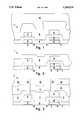
- FIG. 1shows a sectional view of a semiconductor composite which has been processed to include multilevel metallizations
- FIG. 2shows a sectional view of the semiconductor composite of FIG. 1 after a planarization step
- FIG. 3shows a sectional view of the semiconductor composite of FIG. 2 after steps of applying a photoresist and etching to form vias.
- the inventionprovides a process which suppresses sputtering of metal during via etching of semiconductor composites.
- a processfor etching a layer of silicon oxide/nitride in a semiconductor composite.
- the semiconductor compositeincludes an electrically conductive layer underlying the silicon oxide/nitride layer.
- the etchingexposes the electrically conductive layer and provides a via extending through the silicon oxide/nitride layer to the electrically conductive layer.
- the etchingis performed by exposing the silicon oxide/nitride layer to an etching gas in an ionized state in a reaction chamber of a plasma generating device.
- the etching gasincludes a fluoride-containing gas and a passivating gas.
- the passivating gasis present in an amount effective to suppress sputtering of the electrically conductive layer when it is exposed to the etching gas.
- Reactive ion etching(“RIE”) and plasma etching (“PE”) are common methods used to open vias anisotropically through the dielectric to the metal.
- RIEreactive ion etching
- PEplasma etching
- the basic difference between the two etch modesis pressure. That is, RIE is typically below 50 mTorr and PE is typically above 50 mTorr.
- the via sputtering problemexists with either mode of etching.
- a fluorinated gassuch as CF 4 , CHF 3 , CH 2 F 2 , CH 3 F, C 2 F 6 , SF 6 , C n F n+4 or other Freon and mixtures thereof is used in the plasma reactor.
- the fluorinated gasdissociates and reacts with the silicon oxide/nitride to form volatile silicon difluoride or silicon tetrafluoride and carbon monoxide or carbon dioxide.
- a carrier gas such as He, Ne, Ar and Krmay be added to improve the etch rate of the silicon oxide/nitride by providing additional ion bombardment energy to break the strong silicon-oxygen/nitrogen bond.
- the energy needed to break the silicon-oxygen bondis on the order of 200 kcal/mole.
- the underlying materialalso experiences this ionic impact.
- the underlying materialcan sputter or react depending on its composition.
- the underlying metalsputters and deposits on the side walls of the silicon oxide/nitride and photoresist.
- the sputtered metalis not volatile because it is fluorinated.
- the inventionovercomes this problem by adding a passivating gas to the etching gas.
- the passivating gascomprises nitrogen.
- the nitrogenpassivates the underlying aluminum, aluminum alloy (such as Al-Si, Al-Si-Cu, Al-Cu, etc.) titanium, titanium nitride, titanium tungsten or molybdenum electrically conducting layers. It is believed that the nitrogen may combine with the metal to form volatile TiN, AlN, etc. rather than a non-volatile organometallic-polymer. It is also believed that the nitrogen reacts with carbon in the feed gas to free up F and thereby increase the etch rate.
- the etching gas of the inventionallows overetching on the order of 200% or even 350% to be achieved without deleterious redeposition or sputtering of the underlying metal on the side wall of the vias or on the resist.
- FIG. 1shows a semiconductor composite according to an exemplary embodiment of the invention prior to a planarization step.
- the composite 1includes an electrically conductive layer 2 and a layer of silicon oxide/nitride 3 on a substrate 4.
- a layer of previously etched polysilicon 5 on gate oxide 6is provided to detail topology and a silicide 7 and another layer of polysilicon 8 is patterned on a portion of the polysilicon 5.
- the topologycan be defined in other ways such as by LOCOS oxidation.
- a layer of silicon dioxide 9is provided between the electrically conductive layer 2 and the layers of polysilicon 5 and 8.
- the silicon oxide/nitride layer 3is provided above the electrically conductive layer 2 and above the exposed portions of the silicon dioxide layer 9.
- a sacrificial layer 10is provided above the silicon oxide/nitride layer 3.
- FIG. 2shows the composite 1 after an oxide planarization step wherein the sacrificial layer 10 is removed and the silicon oxide/nitride layer 3 has been planarized. As shown in FIG. 2, the silicon oxide/nitride layer 3 is thinner above one region of the electrically conductive layer 2 than above a second region of the electrically conductive layer 2.
- FIG. 3shows the composite 1 after an optional planarizing layer 11 (such as SiO 2 , SiN or SiON) is provided on the silicon oxide/nitride layer 3.
- FIG. 3shows a photoresist layer 12 provided On the planarized layer 11, 3 and vias 13 extending through the photoresist layer 12, the planarizing layer 11 and the silicon oxide/nitride layer 3.
- the short viacould be 5000 ⁇ deep and the longer via could be 21/2 ⁇ m deep.
- the region of the electrically conductive layer 2 on the right side of FIG. 3will be exposed to the etching gas for a longer time than the region of the electrically conductive layer 2 shown on the left side of FIG. 3.
- both regions of the electrically conductive layer 2can be overetched during the etching process such as by at least 200% or even at least 350%.
- the silicon oxide/nitride layer 3can comprise a silicon dioxide layer, a silicon nitride layer or a layer of oxynitride.
- the electrically conductive layer 2can comprise a metal-containing layer such as Al, Al alloys, Ti, TiN, TiW and Mo.
- the remaining layers of the composite 1can comprise conventional materials and the composite 1 can take other forms than that shown in FIGS. 1-3. That is, the embodiment of the composite 1 shown in FIGS. 1-3 is merely for purposes of illustrating how the inventive method can be used to provide vias in a semiconductor composite.
- the etching in accordance with the inventioncan comprise reactive ion etching typically carried out at pressures of 50 mTorr or less or plasma etching typically carried out at pressures above those used for reactive ion etching.
- the etching gasis in an ionized state when it contacts the semiconductor surface being etched.
- the etching gasincludes a fluoride-containing gas and the passivating gas.
- the fluoride-containing gascan comprise CF 4 , CHF 3 , C 2 F 6 , CH 2 F 2 , SF 6 or other Freons and mixtures thereof.
- the etching gascan also include a carrier gas such as Ar, He, Ne, Kr or mixtures thereof.
- the etching gascan be exposed to a microwave electric field and/or a magnetic field during the etching step.
- the flow rates of the various constituents of the etching gasare controlled to provide suitable etching while suppressing sputtering of the electrically conductive layer 2.
- the flow rate of the nitrogencan be at least 10 sccm and the flow rate of the fluoride-containing gas can be 4 to 100 sccm.
- the amount of nitrogen added to the etch gasshould be enough to suppress sputtering of the electrically conductive layer. Although there is no upper limit on the amount of nitrogen which can be added to the gas due to the highly reactive nature of the nitrogen with components of the etching apparatus, the maximum amount of nitrogen should be controlled to prevent the equipment from wearing out.
- the carrier gasis optional.
- argonis the carrier gas
- itcan be added in any amount such as 1 1/min (1000 sccm).
- the oxidecan be etched through in about one minute and overetching of 350% can be performed in about three minutes.
- nitrogento the etching gas, it is possible to totally prevent sputtering or redeposition of Al, Ti or TiN underlying electrically conducting layers during the oxide etch.
- the process of the inventioncan also include steps of forming a photoresist layer on the silicon oxide/nitride layer and patterning the photoresist layer to form a plurality of via holes therein.
- the etching stepforms vias in the silicon oxide/nitride layer corresponding to the via holes in the photoresist layer.
- the process of the inventioncan include a step of planarizing the silicon oxide/nitride layer prior to the etching step. In this case, the silicon oxide/nitride layer can be etched and/or covered with a photoresist or spin-on glass to achieve planarization.
- the process of the inventioncan include a step of depositing a multi-level electrically conductive layer so as to provide first and second regions thereof which are spaced apart and at different levels.
- the planarizing stepdecreases thicknesses of the silicon oxide/nitride layer such that the silicon oxide/nitride layer is thicker above the first region than above the second region, as shown in FIGS. 2 and 3.
- the processcan also include a step of depositing metal on the composite after the etching step so as to fill the vias with metal.
Landscapes
- Engineering & Computer Science (AREA)
- Computer Hardware Design (AREA)
- Physics & Mathematics (AREA)
- Condensed Matter Physics & Semiconductors (AREA)
- General Physics & Mathematics (AREA)
- Manufacturing & Machinery (AREA)
- Chemical & Material Sciences (AREA)
- Microelectronics & Electronic Packaging (AREA)
- Power Engineering (AREA)
- General Chemical & Material Sciences (AREA)
- Inorganic Chemistry (AREA)
- Chemical Kinetics & Catalysis (AREA)
- Drying Of Semiconductors (AREA)
- Internal Circuitry In Semiconductor Integrated Circuit Devices (AREA)
Abstract
Description
The invention relates to an improved plasma etching and reactive ion etching process for opening vias in semiconductor composites.
U.S. Pat. No. 4,973,381 ("Palmer") discloses a process for etching a semiconductor surface with excited gas which is drawn out by a pressure differential through an output opening in a glass or quartz container toward a surface to be etched. The container is placed in a vacuum enclosure at a pressure of 10-4 to 10-5 Torr. The excited species can be a mixture of CCl4 and O2 or an active species such as fluorine and a buffer gas such as He, Ar or N. In Palmer, plasma ions reunite prior to exiting the container and the etching gas will not be in an ionized state when it contacts the wafer.
U.S. Pat. No. 4,978,420 ("Bach") discloses etching vias in a dual-layer comprising SiO2 and silicon nitride. In Bach, the photoresist and nitride layers are etched simultaneously with an etching gas which includes CF4 or SF6, oxygen and argon and the oxide is etched with the same gases except for the absence of oxygen. The power in the plasma reactor is set at 325-350 Watts during the nitride etch and increased to 375 Watts for the oxide etch. A tungsten layer is provided beneath the oxide to resist overetching since W is highly resistant to the oxide etch.
U.S. Pat. No. 4,981,550 ("Huttemann") discloses a process for etching W by exposing a layer of W and a buffer layer to the etching plasma. Huttemann discloses that the buffered layer can be Al and an inert gas such as Ar can be used to sputter clean the buffer layer simultaneously with the plasma etch.
U.S. Pat. No. 4,948,462 ("Rossen") discloses a process for etching W by exposing a W layer to SF6, N2 and Cl2 etching gases.
U.S. Pat. No. 4,617,079 ("Tracy") discloses plasma etching of SiO2 with 200 sccm Ar, 40 sccm CF4 and 40 CHF3.
U.S. Pat. No. 4,407,850 ("Bruce") discloses anisotropic etching of a photoresist under plasma conditions at pressures above those used in reactive ion etching. In particular, etching at rates of 2000 to 300 Å/min was obtained using pressures of 0.3 to 2 Torr and reactive gases O2 and Ar. The background of Bruce mentions that planarizing of rough surface topography allows better focusing using optics with small depths of field. In Bruce, a silicon wafer is coated with a layer of thermal oxide, a 1 μm layer of resist (planarizing layer), a masking layer (1000 Å SiO2) and a 0.5 μm (5000 Å) layer of photoresist. Bruce discloses that the planarizing layer can be Shipley AZ 1350 photoresist.
In prior art plasma etching and reactive ion etching ("RIE") of silicon oxide a fluorinated gas is used as the etching gas. A problem with this type of etching has been sputtering of metal layers and deposition of an organometallic polymer (a carbon-fluorine based polymer which includes the underlying metal) on sidewalls of vias formed during the etching process. Such deposits of organometallic polymer on the sidewalls of the via and photoresist are difficult to remove.
The above problem is even worse when the semiconductor composite includes multiple layers of metal interconnects since dielectric planarization creates various dielectric thicknesses and the etch time to form the vias is based on the thickest oxide step. As a result, the metal underlying the thinner oxide steps is exposed to the etching gas for a longer time thus producing more sputtering of the metal than the metal underlying the thicker oxide steps.
In etching silicon oxide, the fluorinated gas reacts with the oxide to form volatile silicon difluoride or silicon tetrafluoride and carbon monoxide or carbon dioxide. The sputtered metal, however, is not volatile since it is fluorinated. Accordingly, there exists a need in the art for an etch process which can open vias of various oxide depths without metal redeposition or sputtering.
The invention provides a process for etching of silicon oxide/nitride by providing a composite comprising an electrically conductive layer and a layer of silicon oxide/nitride and etching the silicon oxide/nitride layer with an etching gas in an ionized state to expose the electrically conductive layer and form a via extending through the silicon oxide/nitride layer to the electrically conductive layer. The etching is performed with an etching gas in a reaction chamber of a plasma generating device, the etching gas including a fluoride-containing gas and a passivating gas, the passivating gas being present in an amount effective to suppress sputtering of the electrically conductive layer. The passivating gas is preferably nitrogen gas and the etching can comprise plasma etching or reactive ion etching. The etching gas can be exposed to a microwave electric field, a magnetic field or both.
According to various aspects of the invention, the silicon oxide/nitride layer can comprise a silicon dioxide layer, a silicon nitride layer or a layer of oxynitride. The electrically conducting layer can comprise multi-level metal layers and the electrically conductive layer can be a metal-containing layer such as Al, Al alloys, Ti, TiN, TiW or Mo. The fluoride-containing gas can comprise CF4, CHF3, C2 F6, CH2 F2, SF6 and/or other Freons and mixtures thereof. The etching gas can also include a carrier gas such as Ar, He, Ne, Kr or mixtures thereof. The etching gas preferably excludes oxygen gas.
The process of the invention can include a step of planarizing the silicon oxide/nitride layer, forming a photoresist layer on the silicon oxide/nitride, patterning the photoresist layer to form a plurality of vias and depositing metal on the etched composite so as to fill the vias.
FIG. 1 shows a sectional view of a semiconductor composite which has been processed to include multilevel metallizations;
FIG. 2 shows a sectional view of the semiconductor composite of FIG. 1 after a planarization step; and
FIG. 3 shows a sectional view of the semiconductor composite of FIG. 2 after steps of applying a photoresist and etching to form vias.
The invention provides a process which suppresses sputtering of metal during via etching of semiconductor composites.
According to the invention, a process is provided for etching a layer of silicon oxide/nitride in a semiconductor composite. In particular, the semiconductor composite includes an electrically conductive layer underlying the silicon oxide/nitride layer. The etching exposes the electrically conductive layer and provides a via extending through the silicon oxide/nitride layer to the electrically conductive layer. The etching is performed by exposing the silicon oxide/nitride layer to an etching gas in an ionized state in a reaction chamber of a plasma generating device. The etching gas includes a fluoride-containing gas and a passivating gas. The passivating gas is present in an amount effective to suppress sputtering of the electrically conductive layer when it is exposed to the etching gas.
As the packing density of semiconductor devices shrinks and device requirements grow, multiple layers of metal interconnects are becoming more common. The use of dielectric planarization is necessary due to step coverage issues and subsequent metal cracking issues. The introduction of a planarization step, however, creates various dielectric thicknesses within the circuit. Contact to the underlying metal is made by etching holes in the dielectric to the metal, commonly called vias.
When etching the dielectric to form a functional via, an etch time based on the thickest oxide step is necessary. This creates a problem commonly referred to as sputtering, redeposition, crowning or via etch residue. This residue is thought to be a carbon-fluorine based polymer which incorporates the underlying metal into it. This polymer deposits on the sidewalls of the via and photoresist and is very difficult to remove following the via etching step.
Reactive ion etching ("RIE") and plasma etching ("PE") are common methods used to open vias anisotropically through the dielectric to the metal. The basic difference between the two etch modes is pressure. That is, RIE is typically below 50 mTorr and PE is typically above 50 mTorr. The via sputtering problem exists with either mode of etching.
To form vias in silicon oxide/nitride such as silicon dioxide (SiO2) or silicon nitride (SiN) or oxynitride (SiNO), a fluorinated gas such as CF4, CHF3, CH2 F2, CH3 F, C2 F6, SF6, Cn Fn+4 or other Freon and mixtures thereof is used in the plasma reactor. The fluorinated gas dissociates and reacts with the silicon oxide/nitride to form volatile silicon difluoride or silicon tetrafluoride and carbon monoxide or carbon dioxide. A carrier gas such as He, Ne, Ar and Kr may be added to improve the etch rate of the silicon oxide/nitride by providing additional ion bombardment energy to break the strong silicon-oxygen/nitrogen bond. The energy needed to break the silicon-oxygen bond is on the order of 200 kcal/mole. The underlying material also experiences this ionic impact. The underlying material can sputter or react depending on its composition. In the case of via etching, the underlying metal sputters and deposits on the side walls of the silicon oxide/nitride and photoresist. The sputtered metal is not volatile because it is fluorinated. The invention overcomes this problem by adding a passivating gas to the etching gas.
According to the process of the invention, vias of various depths on the circuit can be opened while suppressing metal redeposition or sputtering. In particular, the passivating gas comprises nitrogen. The nitrogen passivates the underlying aluminum, aluminum alloy (such as Al-Si, Al-Si-Cu, Al-Cu, etc.) titanium, titanium nitride, titanium tungsten or molybdenum electrically conducting layers. It is believed that the nitrogen may combine with the metal to form volatile TiN, AlN, etc. rather than a non-volatile organometallic-polymer. It is also believed that the nitrogen reacts with carbon in the feed gas to free up F and thereby increase the etch rate. The etching gas of the invention allows overetching on the order of 200% or even 350% to be achieved without deleterious redeposition or sputtering of the underlying metal on the side wall of the vias or on the resist.
FIG. 1 shows a semiconductor composite according to an exemplary embodiment of the invention prior to a planarization step. In particular, thecomposite 1 includes an electricallyconductive layer 2 and a layer of silicon oxide/nitride 3 on asubstrate 4. A layer of previously etchedpolysilicon 5 ongate oxide 6 is provided to detail topology and asilicide 7 and another layer ofpolysilicon 8 is patterned on a portion of thepolysilicon 5. It should be noted, however, that the topology can be defined in other ways such as by LOCOS oxidation. A layer ofsilicon dioxide 9 is provided between the electricallyconductive layer 2 and the layers ofpolysilicon nitride layer 3 is provided above the electricallyconductive layer 2 and above the exposed portions of thesilicon dioxide layer 9. Asacrificial layer 10 is provided above the silicon oxide/nitride layer 3.
FIG. 2 shows the composite 1 after an oxide planarization step wherein thesacrificial layer 10 is removed and the silicon oxide/nitride layer 3 has been planarized. As shown in FIG. 2, the silicon oxide/nitride layer 3 is thinner above one region of the electricallyconductive layer 2 than above a second region of the electricallyconductive layer 2.
FIG. 3 shows the composite 1 after an optional planarizing layer 11 (such as SiO2, SiN or SiON) is provided on the silicon oxide/nitride layer 3. In addition, FIG. 3 shows aphotoresist layer 12 provided On theplanarized layer photoresist layer 12, theplanarizing layer 11 and the silicon oxide/nitride layer 3. As an example, the short via could be 5000 Å deep and the longer via could be 21/2 μm deep. As can be appreciated from FIG. 3, the region of the electricallyconductive layer 2 on the right side of FIG. 3 will be exposed to the etching gas for a longer time than the region of the electricallyconductive layer 2 shown on the left side of FIG. 3. In order to fully remove the silicon oxide/nitride layer 3, both regions of the electricallyconductive layer 2 can be overetched during the etching process such as by at least 200% or even at least 350%.
The silicon oxide/nitride layer 3 can comprise a silicon dioxide layer, a silicon nitride layer or a layer of oxynitride. The electricallyconductive layer 2 can comprise a metal-containing layer such as Al, Al alloys, Ti, TiN, TiW and Mo. The remaining layers of the composite 1 can comprise conventional materials and the composite 1 can take other forms than that shown in FIGS. 1-3. That is, the embodiment of the composite 1 shown in FIGS. 1-3 is merely for purposes of illustrating how the inventive method can be used to provide vias in a semiconductor composite.
The etching in accordance with the invention can comprise reactive ion etching typically carried out at pressures of 50 mTorr or less or plasma etching typically carried out at pressures above those used for reactive ion etching. In either case, the etching gas is in an ionized state when it contacts the semiconductor surface being etched. The etching gas includes a fluoride-containing gas and the passivating gas. The fluoride-containing gas can comprise CF4, CHF3, C2 F6, CH2 F2, SF6 or other Freons and mixtures thereof. The etching gas can also include a carrier gas such as Ar, He, Ne, Kr or mixtures thereof. The etching gas can be exposed to a microwave electric field and/or a magnetic field during the etching step.
The flow rates of the various constituents of the etching gas are controlled to provide suitable etching while suppressing sputtering of the electricallyconductive layer 2. For instance, the flow rate of the nitrogen can be at least 10 sccm and the flow rate of the fluoride-containing gas can be 4 to 100 sccm. The amount of nitrogen added to the etch gas should be enough to suppress sputtering of the electrically conductive layer. Although there is no upper limit on the amount of nitrogen which can be added to the gas due to the highly reactive nature of the nitrogen with components of the etching apparatus, the maximum amount of nitrogen should be controlled to prevent the equipment from wearing out. The carrier gas is optional. For instance, if argon is the carrier gas, it can be added in any amount such as 1 1/min (1000 sccm). In a typical via etching process, the oxide can be etched through in about one minute and overetching of 350% can be performed in about three minutes. In accordance with the invention, by adding nitrogen to the etching gas, it is possible to totally prevent sputtering or redeposition of Al, Ti or TiN underlying electrically conducting layers during the oxide etch.
The process of the invention can also include steps of forming a photoresist layer on the silicon oxide/nitride layer and patterning the photoresist layer to form a plurality of via holes therein. The etching step forms vias in the silicon oxide/nitride layer corresponding to the via holes in the photoresist layer. Also, the process of the invention can include a step of planarizing the silicon oxide/nitride layer prior to the etching step. In this case, the silicon oxide/nitride layer can be etched and/or covered with a photoresist or spin-on glass to achieve planarization. Furthermore, the process of the invention can include a step of depositing a multi-level electrically conductive layer so as to provide first and second regions thereof which are spaced apart and at different levels. At this case, the planarizing step decreases thicknesses of the silicon oxide/nitride layer such that the silicon oxide/nitride layer is thicker above the first region than above the second region, as shown in FIGS. 2 and 3. The process can also include a step of depositing metal on the composite after the etching step so as to fill the vias with metal.
While the invention has been described with reference to the foregoing embodiments, various changes and modifications can be made thereto which fall within the scope of the following claims.
Claims (19)
1. A process for etching a layer of silicon oxide or silicon nitride or combination thereof, comprising the steps of:
providing a semiconductor composite comprising an electrically conductive layer underlying a layer of silicon oxide or silicon nitride or combination thereof; and
etching the layer of silicon oxide or silicon nitride or combination thereof to expose the electrically conductive layer and provide a via extending through the layer of silicon oxide or silicon nitride or combination thereof to the electrically conductive layer, the etching being performed by exposing the layer of silicon oxide or silicon nitride or combination thereof to an etching gas in an ionized state in a reaction chamber of a plasma generating device, the etching gas including a fluoride-containing gas and a passivating gas, the passivating gas comprising nitrogen which is present in an amount effective to suppress sputtering of the electrically conductive layer when it is exposed to the etching gas during the etching step.
2. The process of claim 1, wherein the layer of silicon oxide or silicon nitride or combination thereof comprises a silicon dioxide layer.
3. The process of claim 1, wherein the etching step comprises reactive ion etching.
4. The process of claim 1, wherein the etching step comprises plasma etching.
5. The process of claim 1, wherein the etching gas consists essentially of the fluoride-containing gas and the nitrogen gas.
6. The process of claim 1, wherein the electrically conductive layer comprises a metal-containing layer selected from the group consisting of Al, Al alloys, Ti, TiN, TiW and Mo.
7. The process of claim 1, wherein the layer of silicon oxide or silicon nitride or combination thereof comprises a layer of oxynitride.
8. The process of claim 1, wherein the fluoride-containing gas comprises a gas selected from the group consisting of CF4, CHF3, CH3 F, C2 F6, CH2 F2, SF6, Cn Fn+4 and mixtures thereof.
9. The process of claim 1, wherein the etching gas includes a carrier gas selected from the group consisting of Ar, He, Ne, Kr or mixtures thereof.
10. The process of claim 1, wherein the etching gas is exposed to a microwave electric field during the etching step.
11. The process of claim 1, wherein the etching gas is exposed to a magnetic field during the etching step.
12. The process of claim 1, wherein the etching gas is exposed to a microwave electric field and a magnetic field during the etching step.
13. The process of claim 1, wherein the passivating gas comprises N2 and during the etching step a flow rate of the N2 is at least 10 sccm and a flow rate of the fluoride-containing gas is 4 to 100 sccm.
14. The process of claim 1, further comprising depositing metal on the composite after the etching step so as to fill the via with metal.
15. The process of claim 1, wherein the etching step is carried out until at least 200% over etching is achieved.
16. The process of claim 1, further comprising steps of forming a photoresist layer on the layer of silicon oxide or silicon nitride or combination thereof, patterning the photoresist layer to form a plurality of via holes therein and the etching step forms vias in the layer of silicon oxide or silicon nitride or combination thereof corresponding to the via holes in the photoresist layer.
17. The process of claim 1, further comprising a step of planarizing the layer of silicon oxide or silicon nitride or combination thereof prior to the etching step.
18. The process of claim 16, further comprising a step of planarizing the layer of silicon oxide or silicon nitride or combination thereof prior to the etching step.
19. The process of claim 18, further comprising a step of depositing the electrically conductive layer so as to provide first and second regions thereof which are spaced apart and at different levels, the planarizing step decreasing thicknesses of the layer of silicon oxide or silicon nitride or combination thereof such that the layer of silicon oxide or silicon nitride or combination thereof is thicker above the first region than above the second region.
Priority Applications (2)
| Application Number | Priority Date | Filing Date | Title |
|---|---|---|---|
| US07/777,611US5269879A (en) | 1991-10-16 | 1991-10-16 | Method of etching vias without sputtering of underlying electrically conductive layer |
| US08/474,003US5658425A (en) | 1991-10-16 | 1995-06-07 | Method of etching contact openings with reduced removal rate of underlying electrically conductive titanium silicide layer |
Applications Claiming Priority (1)
| Application Number | Priority Date | Filing Date | Title |
|---|---|---|---|
| US07/777,611US5269879A (en) | 1991-10-16 | 1991-10-16 | Method of etching vias without sputtering of underlying electrically conductive layer |
Related Child Applications (1)
| Application Number | Title | Priority Date | Filing Date |
|---|---|---|---|
| US16591493AContinuation-In-Part | 1991-10-16 | 1993-12-14 |
Publications (1)
| Publication Number | Publication Date |
|---|---|
| US5269879Atrue US5269879A (en) | 1993-12-14 |
Family
ID=25110734
Family Applications (1)
| Application Number | Title | Priority Date | Filing Date |
|---|---|---|---|
| US07/777,611Expired - LifetimeUS5269879A (en) | 1991-10-16 | 1991-10-16 | Method of etching vias without sputtering of underlying electrically conductive layer |
Country Status (1)
| Country | Link |
|---|---|
| US (1) | US5269879A (en) |
Cited By (81)
| Publication number | Priority date | Publication date | Assignee | Title |
|---|---|---|---|---|
| EP0655775A1 (en)* | 1993-11-30 | 1995-05-31 | Advanced Micro Devices, Inc. | Dry etching process for SIOX compounds |
| US5468339A (en)* | 1992-10-09 | 1995-11-21 | Advanced Micro Devices, Inc. | Plasma etch process |
| US5549786A (en)* | 1995-08-29 | 1996-08-27 | Advanced Micro Devices, Inc. | Highly selective, highly uniform plasma etch process for spin-on glass |
| US5626716A (en)* | 1995-09-29 | 1997-05-06 | Lam Research Corporation | Plasma etching of semiconductors |
| US5650897A (en)* | 1992-07-21 | 1997-07-22 | Seagate Technology, Inc. | Thin film magnetic head including lightning arrester and process for making the same |
| US5657192A (en)* | 1992-07-21 | 1997-08-12 | Seagate Technology, Inc. | Thin film magnetic head including crater for recessed structure and process for making the same |
| EP0691678A3 (en)* | 1994-07-08 | 1997-10-01 | Applied Materials Inc | Method of etching contact holes in a dielectric layer by plasma, with removal of residues |
| US5700737A (en)* | 1996-02-26 | 1997-12-23 | Taiwan Semiconductor Manufactured Company Ltd. | PECVD silicon nitride for etch stop mask and ozone TEOS pattern sensitivity elimination |
| US5780343A (en)* | 1995-12-20 | 1998-07-14 | National Semiconductor Corporation | Method of producing high quality silicon surface for selective epitaxial growth of silicon |
| US5843846A (en)* | 1996-12-31 | 1998-12-01 | Intel Corporation | Etch process to produce rounded top corners for sub-micron silicon trench applications |
| US5843847A (en)* | 1996-04-29 | 1998-12-01 | Applied Materials, Inc. | Method for etching dielectric layers with high selectivity and low microloading |
| US5854124A (en)* | 1997-02-04 | 1998-12-29 | Winbond Electronics Corp. | Method for opening contacts of different depths in a semiconductor wafer |
| WO1999010923A1 (en)* | 1997-08-28 | 1999-03-04 | Lam Research Corporation | Method for selective plasma etch |
| US5880037A (en)* | 1992-09-08 | 1999-03-09 | Applied Materials, Inc. | Oxide etch process using a mixture of a fluorine-substituted hydrocarbon and acetylene that provides high selectivity to nitride and is suitable for use on surfaces of uneven topography |
| WO1999021217A1 (en)* | 1997-10-22 | 1999-04-29 | Interuniversitair Micro-Elektronica Centrum | Anisotropic etching of organic-containing insulating layers |
| US5904566A (en)* | 1997-06-09 | 1999-05-18 | Taiwan Semiconductor Manufacturing Company, Ltd. | Reactive ion etch method for forming vias through nitrogenated silicon oxide layers |
| US5906948A (en)* | 1998-04-17 | 1999-05-25 | Vanguard International Semiconductor Corporation | Method for etching high aspect-ratio multilevel contacts |
| US5935877A (en)* | 1995-09-01 | 1999-08-10 | Applied Materials, Inc. | Etch process for forming contacts over titanium silicide |
| FR2775830A1 (en)* | 1998-03-09 | 1999-09-10 | United Microelectronics Corp | PROCESS FOR ATTACKING SILICON NITRIDE |
| US5962344A (en)* | 1997-12-29 | 1999-10-05 | Vanguard International Semiconductor Corporation | Plasma treatment method for PECVD silicon nitride films for improved passivation layers on semiconductor metal interconnections |
| US6013582A (en)* | 1997-12-08 | 2000-01-11 | Applied Materials, Inc. | Method for etching silicon oxynitride and inorganic antireflection coatings |
| US6019906A (en)* | 1998-05-29 | 2000-02-01 | Taiwan Semiconductor Manufacturing Company | Hard masking method for forming patterned oxygen containing plasma etchable layer |
| US6025273A (en)* | 1998-04-06 | 2000-02-15 | Taiwan Semiconductor Manufacturing Company, Ltd. | Method for etching reliable small contact holes with improved profiles for semiconductor integrated circuits using a carbon doped hard mask |
| US6063711A (en)* | 1998-04-28 | 2000-05-16 | Taiwan Semiconductor Manufacturing Company | High selectivity etching stop layer for damascene process |
| US6069087A (en)* | 1998-08-25 | 2000-05-30 | Micron Technology, Inc. | Highly selective dry etching process |
| US6074572A (en)* | 1999-04-06 | 2000-06-13 | Cryogen, Inc. | Gas mixture for cryogenic applications |
| US6074952A (en)* | 1998-05-07 | 2000-06-13 | Vanguard International Semiconductor Corporation | Method for forming multi-level contacts |
| US6074958A (en)* | 1994-06-13 | 2000-06-13 | Hitachi, Ltd. | Semiconductor integrated circuit arrangement fabrication method |
| US6077781A (en)* | 1995-11-21 | 2000-06-20 | Applied Materials, Inc. | Single step process for blanket-selective CVD aluminum deposition |
| US6080680A (en)* | 1997-12-19 | 2000-06-27 | Lam Research Corporation | Method and composition for dry etching in semiconductor fabrication |
| US6083844A (en)* | 1997-12-22 | 2000-07-04 | Lam Research Corporation | Techniques for etching an oxide layer |
| US6107215A (en)* | 1997-05-23 | 2000-08-22 | Fujitsu Limited | Hydrogen plasma downstream treatment equipment and hydrogen plasma downstream treatment method |
| US6117793A (en)* | 1998-09-03 | 2000-09-12 | Micron Technology, Inc. | Using silicide cap as an etch stop for multilayer metal process and structures so formed |
| US6117786A (en)* | 1998-05-05 | 2000-09-12 | Lam Research Corporation | Method for etching silicon dioxide using fluorocarbon gas chemistry |
| US6124212A (en)* | 1997-10-08 | 2000-09-26 | Taiwan Semiconductor Manufacturing Co. | High density plasma (HDP) etch method for suppressing micro-loading effects when etching polysilicon layers |
| US6136663A (en)* | 1998-03-09 | 2000-10-24 | United Microelectronics Corp. | Method of etching silicon nitride |
| US6136712A (en)* | 1998-09-30 | 2000-10-24 | Lam Research Corporation | Method and apparatus for improving accuracy of plasma etching process |
| US6184119B1 (en)* | 1999-03-15 | 2001-02-06 | Vlsi Technology, Inc. | Methods for reducing semiconductor contact resistance |
| US6184150B1 (en) | 1992-09-08 | 2001-02-06 | Applied Materials Inc. | Oxide etch process with high selectivity to nitride suitable for use on surfaces of uneven topography |
| US6214742B1 (en)* | 1998-12-07 | 2001-04-10 | Advanced Micro Devices, Inc. | Post-via tin removal for via resistance improvement |
| US6228279B1 (en)* | 1998-09-17 | 2001-05-08 | International Business Machines Corporation | High-density plasma, organic anti-reflective coating etch system compatible with sensitive photoresist materials |
| US6245682B1 (en) | 1999-03-11 | 2001-06-12 | Taiwan Semiconductor Manufacturing Company | Removal of SiON ARC film after poly photo and etch |
| US6281132B1 (en)* | 1998-10-06 | 2001-08-28 | Advanced Micro Devices, Inc. | Device and method for etching nitride spacers formed upon an integrated circuit gate conductor |
| US6287978B1 (en)* | 1992-06-15 | 2001-09-11 | Micron Technology, Inc. | Method of etching a substrate |
| US6291356B1 (en) | 1997-12-08 | 2001-09-18 | Applied Materials, Inc. | Method for etching silicon oxynitride and dielectric antireflection coatings |
| US6297163B1 (en) | 1998-09-30 | 2001-10-02 | Lam Research Corporation | Method of plasma etching dielectric materials |
| US6303045B1 (en)* | 1997-03-20 | 2001-10-16 | Lam Research Corporation | Methods and apparatus for etching a nitride layer in a variable-gap plasma processing chamber |
| US6319822B1 (en)* | 1998-10-01 | 2001-11-20 | Taiwan Semiconductor Manufacturing Company | Process for forming an integrated contact or via |
| US6326296B1 (en)* | 1998-07-01 | 2001-12-04 | Taiwan Semiconductor Manufacturing Company | Method of forming dual damascene structure with improved contact/via edge integrity |
| US6329292B1 (en)* | 1998-07-09 | 2001-12-11 | Applied Materials, Inc. | Integrated self aligned contact etch |
| US6391212B1 (en) | 1992-10-20 | 2002-05-21 | Uri Cohen | Method for etching gap-vias in a magnetic thin film head and product |
| US6391786B1 (en) | 1997-12-31 | 2002-05-21 | Lam Research Corporation | Etching process for organic anti-reflective coating |
| US6444564B1 (en) | 1998-11-23 | 2002-09-03 | Advanced Micro Devices, Inc. | Method and product for improved use of low k dielectric material among integrated circuit interconnect structures |
| US6492279B1 (en) | 2000-01-27 | 2002-12-10 | Micron Technology, Inc. | Plasma etching methods |
| US20030024808A1 (en)* | 2001-01-04 | 2003-02-06 | Hilke Donohue | Methods of sputtering using krypton |
| US20030024902A1 (en)* | 2001-03-30 | 2003-02-06 | Li Si Yi | Method of plasma etching low-k dielectric materials |
| US6569774B1 (en) | 2000-08-31 | 2003-05-27 | Micron Technology, Inc. | Method to eliminate striations and surface roughness caused by dry etch |
| US6576547B2 (en) | 1998-03-05 | 2003-06-10 | Micron Technology, Inc. | Residue-free contact openings and methods for fabricating same |
| US6593230B1 (en)* | 1998-01-14 | 2003-07-15 | Ricoh Company, Ltd. | Method of manufacturing semiconductor device |
| US20030162407A1 (en)* | 1997-10-22 | 2003-08-28 | Karen Maex | Anisotropic etching of organic-containing insulating layers |
| US6617257B2 (en) | 2001-03-30 | 2003-09-09 | Lam Research Corporation | Method of plasma etching organic antireflective coating |
| US6630407B2 (en) | 2001-03-30 | 2003-10-07 | Lam Research Corporation | Plasma etching of organic antireflective coating |
| EP1096562A3 (en)* | 1999-10-29 | 2003-12-17 | Lucent Technologies Inc. | Method for making a semiconductor device |
| US6706640B1 (en)* | 2002-11-12 | 2004-03-16 | Taiwan Semiconductor Manufacturing Co., Ltd | Metal silicide etch resistant plasma etch method |
| US6746961B2 (en) | 2001-06-19 | 2004-06-08 | Lam Research Corporation | Plasma etching of dielectric layer with etch profile control |
| US20040175945A1 (en)* | 1997-10-22 | 2004-09-09 | Serge Vanhaelemeersch | Anisotropic etching of organic-containing insulating layers |
| US20040248413A1 (en)* | 2000-04-27 | 2004-12-09 | Micron Technology, Inc. | Etchant and method of use |
| US20050176237A1 (en)* | 2004-02-05 | 2005-08-11 | Standaert Theodorus E. | In-situ liner formation during reactive ion etch |
| US20050186801A1 (en)* | 1999-06-24 | 2005-08-25 | Shouochi Uno | Method of manufacture of semiconductor integrated circuit |
| US20050211672A1 (en)* | 2001-08-30 | 2005-09-29 | Kei-Yu Ko | Etch-processing apparatus |
| US6967408B1 (en) | 1997-04-30 | 2005-11-22 | Micron Technology, Inc. | Gate stack structure |
| US7026010B1 (en) | 2002-04-10 | 2006-04-11 | Seagate Technology Llc | Coupling enhancement for medium with anti-ferromagnetic coupling |
| US20060154472A1 (en)* | 2005-01-13 | 2006-07-13 | Tokyo Electron Limited | Etching method, program, computer readable storage medium and plasma processing apparatus |
| KR100761563B1 (en)* | 2005-01-13 | 2007-09-27 | 동경 엘렉트론 주식회사 | Etching method, program, computer readable storage medium and plasma processing apparatus |
| USRE39895E1 (en) | 1994-06-13 | 2007-10-23 | Renesas Technology Corp. | Semiconductor integrated circuit arrangement fabrication method |
| US20080057724A1 (en)* | 2006-08-31 | 2008-03-06 | Mark Kiehlbauch | Selective etch chemistries for forming high aspect ratio features and associated structures |
| CN100377316C (en)* | 1998-05-12 | 2008-03-26 | 世界先进积体电路股份有限公司 | Method for forming multiple contact windows with different depths |
| US7682985B2 (en) | 2004-03-17 | 2010-03-23 | Lam Research Corporation | Dual doped polysilicon and silicon germanium etch |
| US10964653B2 (en) | 2017-09-28 | 2021-03-30 | Taiwan Semiconductor Manufacturing Co., Ltd. | Method of forming a semiconductor device comprising top conductive pads |
| CN114879394A (en)* | 2022-04-29 | 2022-08-09 | 深圳市华星光电半导体显示技术有限公司 | Display panel and manufacturing method thereof |
| US20230043874A1 (en)* | 2021-08-04 | 2023-02-09 | Changxin Memory Technologies, Inc. | Semiconductor structure and manufacturing method thereof |
Citations (13)
| Publication number | Priority date | Publication date | Assignee | Title |
|---|---|---|---|---|
| US4407850A (en)* | 1982-01-11 | 1983-10-04 | The Perkin-Elmer Corporation | Profile control photoresist |
| US4473436A (en)* | 1982-05-05 | 1984-09-25 | Siemens Aktiengesellschaft | Method of producing structures from double layers of metal silicide and polysilicon on integrated circuit substrates by RIE utilizing SF6 and Cl2 |
| US4617079A (en)* | 1985-04-12 | 1986-10-14 | The Perkin Elmer Corporation | Plasma etching system |
| US4784720A (en)* | 1985-05-03 | 1988-11-15 | Texas Instruments Incorporated | Trench etch process for a single-wafer RIE dry etch reactor |
| US4844773A (en)* | 1987-07-16 | 1989-07-04 | Texas Instruments Incorporated | Process for etching silicon nitride film |
| US4908333A (en)* | 1987-03-24 | 1990-03-13 | Oki Electric Industry Co., Ltd. | Process for manufacturing a semiconductor device having a contact window defined by an inclined surface of a composite film |
| US4948462A (en)* | 1989-10-20 | 1990-08-14 | Applied Materials, Inc. | Tungsten etch process with high selectivity to photoresist |
| US4948459A (en)* | 1988-01-20 | 1990-08-14 | U.S. Philips Corporation | Method of enabling electrical connection to a substructure forming part of an electronic device |
| US4973381A (en)* | 1987-11-30 | 1990-11-27 | Texas Instruments Incorporated | Method and apparatus for etching surface with excited gas |
| US4978420A (en)* | 1990-01-03 | 1990-12-18 | Hewlett-Packard Company | Single chamber via etch through a dual-layer dielectric |
| US4981550A (en)* | 1987-09-25 | 1991-01-01 | At&T Bell Laboratories | Semiconductor device having tungsten plugs |
| US5006485A (en)* | 1988-12-09 | 1991-04-09 | U.S. Philips Corporation | Method of manufacturing an intergrated circuit including steps for forming interconnections between patterns formed at different levels |
| US5022958A (en)* | 1990-06-27 | 1991-06-11 | At&T Bell Laboratories | Method of etching for integrated circuits with planarized dielectric |
- 1991
- 1991-10-16USUS07/777,611patent/US5269879A/ennot_activeExpired - Lifetime
Patent Citations (13)
| Publication number | Priority date | Publication date | Assignee | Title |
|---|---|---|---|---|
| US4407850A (en)* | 1982-01-11 | 1983-10-04 | The Perkin-Elmer Corporation | Profile control photoresist |
| US4473436A (en)* | 1982-05-05 | 1984-09-25 | Siemens Aktiengesellschaft | Method of producing structures from double layers of metal silicide and polysilicon on integrated circuit substrates by RIE utilizing SF6 and Cl2 |
| US4617079A (en)* | 1985-04-12 | 1986-10-14 | The Perkin Elmer Corporation | Plasma etching system |
| US4784720A (en)* | 1985-05-03 | 1988-11-15 | Texas Instruments Incorporated | Trench etch process for a single-wafer RIE dry etch reactor |
| US4908333A (en)* | 1987-03-24 | 1990-03-13 | Oki Electric Industry Co., Ltd. | Process for manufacturing a semiconductor device having a contact window defined by an inclined surface of a composite film |
| US4844773A (en)* | 1987-07-16 | 1989-07-04 | Texas Instruments Incorporated | Process for etching silicon nitride film |
| US4981550A (en)* | 1987-09-25 | 1991-01-01 | At&T Bell Laboratories | Semiconductor device having tungsten plugs |
| US4973381A (en)* | 1987-11-30 | 1990-11-27 | Texas Instruments Incorporated | Method and apparatus for etching surface with excited gas |
| US4948459A (en)* | 1988-01-20 | 1990-08-14 | U.S. Philips Corporation | Method of enabling electrical connection to a substructure forming part of an electronic device |
| US5006485A (en)* | 1988-12-09 | 1991-04-09 | U.S. Philips Corporation | Method of manufacturing an intergrated circuit including steps for forming interconnections between patterns formed at different levels |
| US4948462A (en)* | 1989-10-20 | 1990-08-14 | Applied Materials, Inc. | Tungsten etch process with high selectivity to photoresist |
| US4978420A (en)* | 1990-01-03 | 1990-12-18 | Hewlett-Packard Company | Single chamber via etch through a dual-layer dielectric |
| US5022958A (en)* | 1990-06-27 | 1991-06-11 | At&T Bell Laboratories | Method of etching for integrated circuits with planarized dielectric |
Cited By (132)
| Publication number | Priority date | Publication date | Assignee | Title |
|---|---|---|---|---|
| US7049244B2 (en) | 1992-06-15 | 2006-05-23 | Micron Technology, Inc. | Method for enhancing silicon dioxide to silicon nitride selectivity |
| US20020000423A1 (en)* | 1992-06-15 | 2002-01-03 | Micron Technologies, Inc. | Method for enhancing oxide to nitride selectivity through the use of independent heat control |
| US6287978B1 (en)* | 1992-06-15 | 2001-09-11 | Micron Technology, Inc. | Method of etching a substrate |
| US6635184B1 (en) | 1992-07-21 | 2003-10-21 | Uri Cohen | Method for pattern-etching alumina layers and products |
| US6059984A (en)* | 1992-07-21 | 2000-05-09 | Seagate Technology, Inc. | Process for fabricating thin film magnetic head including crater for recessed structure |
| US5650897A (en)* | 1992-07-21 | 1997-07-22 | Seagate Technology, Inc. | Thin film magnetic head including lightning arrester and process for making the same |
| US5657192A (en)* | 1992-07-21 | 1997-08-12 | Seagate Technology, Inc. | Thin film magnetic head including crater for recessed structure and process for making the same |
| US5659451A (en)* | 1992-07-21 | 1997-08-19 | Seagate Technology, Inc. | Studless thin film magnetic head and process for making the same |
| US5835315A (en)* | 1992-07-21 | 1998-11-10 | Seagate Technology, Inc. | Wafer including scribe line grooves for separating thin film heads and process for making the same |
| US5820770A (en)* | 1992-07-21 | 1998-10-13 | Seagate Technology, Inc. | Thin film magnetic head including vias formed in alumina layer and process for making the same |
| US6184150B1 (en) | 1992-09-08 | 2001-02-06 | Applied Materials Inc. | Oxide etch process with high selectivity to nitride suitable for use on surfaces of uneven topography |
| US5880037A (en)* | 1992-09-08 | 1999-03-09 | Applied Materials, Inc. | Oxide etch process using a mixture of a fluorine-substituted hydrocarbon and acetylene that provides high selectivity to nitride and is suitable for use on surfaces of uneven topography |
| US5468340A (en)* | 1992-10-09 | 1995-11-21 | Gupta; Subhash | Highly selective high aspect ratio oxide etch method and products made by the process |
| US5468339A (en)* | 1992-10-09 | 1995-11-21 | Advanced Micro Devices, Inc. | Plasma etch process |
| US6391212B1 (en) | 1992-10-20 | 2002-05-21 | Uri Cohen | Method for etching gap-vias in a magnetic thin film head and product |
| EP0655775A1 (en)* | 1993-11-30 | 1995-05-31 | Advanced Micro Devices, Inc. | Dry etching process for SIOX compounds |
| US6074958A (en)* | 1994-06-13 | 2000-06-13 | Hitachi, Ltd. | Semiconductor integrated circuit arrangement fabrication method |
| USRE39895E1 (en) | 1994-06-13 | 2007-10-23 | Renesas Technology Corp. | Semiconductor integrated circuit arrangement fabrication method |
| US6309980B1 (en) | 1994-06-13 | 2001-10-30 | Hitachi, Ltd. | Semiconductor integrated circuit arrangement fabrication method |
| EP0691678A3 (en)* | 1994-07-08 | 1997-10-01 | Applied Materials Inc | Method of etching contact holes in a dielectric layer by plasma, with removal of residues |
| US5549786A (en)* | 1995-08-29 | 1996-08-27 | Advanced Micro Devices, Inc. | Highly selective, highly uniform plasma etch process for spin-on glass |
| US5935877A (en)* | 1995-09-01 | 1999-08-10 | Applied Materials, Inc. | Etch process for forming contacts over titanium silicide |
| US5626716A (en)* | 1995-09-29 | 1997-05-06 | Lam Research Corporation | Plasma etching of semiconductors |
| US6458684B1 (en) | 1995-11-21 | 2002-10-01 | Applied Materials, Inc. | Single step process for blanket-selective CVD aluminum deposition |
| US6077781A (en)* | 1995-11-21 | 2000-06-20 | Applied Materials, Inc. | Single step process for blanket-selective CVD aluminum deposition |
| US5780343A (en)* | 1995-12-20 | 1998-07-14 | National Semiconductor Corporation | Method of producing high quality silicon surface for selective epitaxial growth of silicon |
| US5700737A (en)* | 1996-02-26 | 1997-12-23 | Taiwan Semiconductor Manufactured Company Ltd. | PECVD silicon nitride for etch stop mask and ozone TEOS pattern sensitivity elimination |
| US5843847A (en)* | 1996-04-29 | 1998-12-01 | Applied Materials, Inc. | Method for etching dielectric layers with high selectivity and low microloading |
| US5843846A (en)* | 1996-12-31 | 1998-12-01 | Intel Corporation | Etch process to produce rounded top corners for sub-micron silicon trench applications |
| US5854124A (en)* | 1997-02-04 | 1998-12-29 | Winbond Electronics Corp. | Method for opening contacts of different depths in a semiconductor wafer |
| US6303045B1 (en)* | 1997-03-20 | 2001-10-16 | Lam Research Corporation | Methods and apparatus for etching a nitride layer in a variable-gap plasma processing chamber |
| US6967408B1 (en) | 1997-04-30 | 2005-11-22 | Micron Technology, Inc. | Gate stack structure |
| US6107215A (en)* | 1997-05-23 | 2000-08-22 | Fujitsu Limited | Hydrogen plasma downstream treatment equipment and hydrogen plasma downstream treatment method |
| US5904566A (en)* | 1997-06-09 | 1999-05-18 | Taiwan Semiconductor Manufacturing Company, Ltd. | Reactive ion etch method for forming vias through nitrogenated silicon oxide layers |
| US6090304A (en)* | 1997-08-28 | 2000-07-18 | Lam Research Corporation | Methods for selective plasma etch |
| WO1999010923A1 (en)* | 1997-08-28 | 1999-03-04 | Lam Research Corporation | Method for selective plasma etch |
| US6124212A (en)* | 1997-10-08 | 2000-09-26 | Taiwan Semiconductor Manufacturing Co. | High density plasma (HDP) etch method for suppressing micro-loading effects when etching polysilicon layers |
| US20030162407A1 (en)* | 1997-10-22 | 2003-08-28 | Karen Maex | Anisotropic etching of organic-containing insulating layers |
| US6900140B2 (en) | 1997-10-22 | 2005-05-31 | Interuniversitair Microelektronica Centrum (Imec) | Anisotropic etching of organic-containing insulating layers |
| WO1999021217A1 (en)* | 1997-10-22 | 1999-04-29 | Interuniversitair Micro-Elektronica Centrum | Anisotropic etching of organic-containing insulating layers |
| US20040175945A1 (en)* | 1997-10-22 | 2004-09-09 | Serge Vanhaelemeersch | Anisotropic etching of organic-containing insulating layers |
| US6844267B1 (en) | 1997-10-22 | 2005-01-18 | Interuniversitair Micro-Elektronica Centrum | Anisotropic etching of organic-containing insulating layers |
| US6844266B2 (en) | 1997-10-22 | 2005-01-18 | Interuniversitair Microelektronica Centrum | Anisotropic etching of organic-containing insulating layers |
| US6291356B1 (en) | 1997-12-08 | 2001-09-18 | Applied Materials, Inc. | Method for etching silicon oxynitride and dielectric antireflection coatings |
| US6013582A (en)* | 1997-12-08 | 2000-01-11 | Applied Materials, Inc. | Method for etching silicon oxynitride and inorganic antireflection coatings |
| US6537918B2 (en) | 1997-12-08 | 2003-03-25 | Applied Materials Inc. | Method for etching silicon oxynitride and dielectric antireflection coatings |
| US6080680A (en)* | 1997-12-19 | 2000-06-27 | Lam Research Corporation | Method and composition for dry etching in semiconductor fabrication |
| US6083844A (en)* | 1997-12-22 | 2000-07-04 | Lam Research Corporation | Techniques for etching an oxide layer |
| US5962344A (en)* | 1997-12-29 | 1999-10-05 | Vanguard International Semiconductor Corporation | Plasma treatment method for PECVD silicon nitride films for improved passivation layers on semiconductor metal interconnections |
| US6391786B1 (en) | 1997-12-31 | 2002-05-21 | Lam Research Corporation | Etching process for organic anti-reflective coating |
| US6593230B1 (en)* | 1998-01-14 | 2003-07-15 | Ricoh Company, Ltd. | Method of manufacturing semiconductor device |
| US6828228B2 (en) | 1998-03-05 | 2004-12-07 | Micron Technology, Inc. | Methods for fabricating residue-free contact openings |
| US7470631B1 (en) | 1998-03-05 | 2008-12-30 | Micron Technology, Inc. | Methods for fabricating residue-free contact openings |
| US6576547B2 (en) | 1998-03-05 | 2003-06-10 | Micron Technology, Inc. | Residue-free contact openings and methods for fabricating same |
| US7700497B2 (en) | 1998-03-05 | 2010-04-20 | Micron Technology, Inc. | Methods for fabricating residue-free contact openings |
| US6747359B1 (en) | 1998-03-05 | 2004-06-08 | Micron Technology, Inc. | Residue-free contact openings and methods for fabricating same |
| US20090104767A1 (en)* | 1998-03-05 | 2009-04-23 | Micron Technology, Inc. | Methods for fabricating residue-free contact openings |
| NL1009202C2 (en)* | 1998-03-09 | 1999-11-22 | United Microelectronics Corp | Method for etching silicon nitride. |
| FR2775830A1 (en)* | 1998-03-09 | 1999-09-10 | United Microelectronics Corp | PROCESS FOR ATTACKING SILICON NITRIDE |
| DE19821452B4 (en)* | 1998-03-09 | 2005-02-17 | United Microelectronics Corp. | A method of making a shallow trench isolation in a semiconductor substrate |
| US6136663A (en)* | 1998-03-09 | 2000-10-24 | United Microelectronics Corp. | Method of etching silicon nitride |
| GB2337026B (en)* | 1998-03-09 | 2000-11-08 | United Microelectronics Corp | Method of etching silicon nitride |
| US6025273A (en)* | 1998-04-06 | 2000-02-15 | Taiwan Semiconductor Manufacturing Company, Ltd. | Method for etching reliable small contact holes with improved profiles for semiconductor integrated circuits using a carbon doped hard mask |
| US5906948A (en)* | 1998-04-17 | 1999-05-25 | Vanguard International Semiconductor Corporation | Method for etching high aspect-ratio multilevel contacts |
| US6063711A (en)* | 1998-04-28 | 2000-05-16 | Taiwan Semiconductor Manufacturing Company | High selectivity etching stop layer for damascene process |
| US6117786A (en)* | 1998-05-05 | 2000-09-12 | Lam Research Corporation | Method for etching silicon dioxide using fluorocarbon gas chemistry |
| US6074952A (en)* | 1998-05-07 | 2000-06-13 | Vanguard International Semiconductor Corporation | Method for forming multi-level contacts |
| CN100377316C (en)* | 1998-05-12 | 2008-03-26 | 世界先进积体电路股份有限公司 | Method for forming multiple contact windows with different depths |
| US6019906A (en)* | 1998-05-29 | 2000-02-01 | Taiwan Semiconductor Manufacturing Company | Hard masking method for forming patterned oxygen containing plasma etchable layer |
| USRE39273E1 (en)* | 1998-05-29 | 2006-09-12 | Taiwan Semiconductor Manufacturing Company, Ltd. | Hard masking method for forming patterned oxygen containing plasma etchable layer |
| US6326296B1 (en)* | 1998-07-01 | 2001-12-04 | Taiwan Semiconductor Manufacturing Company | Method of forming dual damascene structure with improved contact/via edge integrity |
| US6329292B1 (en)* | 1998-07-09 | 2001-12-11 | Applied Materials, Inc. | Integrated self aligned contact etch |
| US6069087A (en)* | 1998-08-25 | 2000-05-30 | Micron Technology, Inc. | Highly selective dry etching process |
| US6703709B1 (en) | 1998-09-03 | 2004-03-09 | Micron Technology, Inc. | Structures formed using silicide cap as an etch stop in multilayer metal processes |
| US6117793A (en)* | 1998-09-03 | 2000-09-12 | Micron Technology, Inc. | Using silicide cap as an etch stop for multilayer metal process and structures so formed |
| US6228279B1 (en)* | 1998-09-17 | 2001-05-08 | International Business Machines Corporation | High-density plasma, organic anti-reflective coating etch system compatible with sensitive photoresist materials |
| US6136712A (en)* | 1998-09-30 | 2000-10-24 | Lam Research Corporation | Method and apparatus for improving accuracy of plasma etching process |
| US6270622B1 (en) | 1998-09-30 | 2001-08-07 | Lam Research Corporation | Method and apparatus for improving accuracy of plasma etching process |
| US6297163B1 (en) | 1998-09-30 | 2001-10-02 | Lam Research Corporation | Method of plasma etching dielectric materials |
| US6319822B1 (en)* | 1998-10-01 | 2001-11-20 | Taiwan Semiconductor Manufacturing Company | Process for forming an integrated contact or via |
| US6281132B1 (en)* | 1998-10-06 | 2001-08-28 | Advanced Micro Devices, Inc. | Device and method for etching nitride spacers formed upon an integrated circuit gate conductor |
| US6444564B1 (en) | 1998-11-23 | 2002-09-03 | Advanced Micro Devices, Inc. | Method and product for improved use of low k dielectric material among integrated circuit interconnect structures |
| US6214742B1 (en)* | 1998-12-07 | 2001-04-10 | Advanced Micro Devices, Inc. | Post-via tin removal for via resistance improvement |
| US6245682B1 (en) | 1999-03-11 | 2001-06-12 | Taiwan Semiconductor Manufacturing Company | Removal of SiON ARC film after poly photo and etch |
| US6184119B1 (en)* | 1999-03-15 | 2001-02-06 | Vlsi Technology, Inc. | Methods for reducing semiconductor contact resistance |
| US6383918B1 (en)* | 1999-03-15 | 2002-05-07 | Philips Electronics | Method for reducing semiconductor contact resistance |
| WO2000060022A1 (en)* | 1999-04-06 | 2000-10-12 | Cryogen, Inc. | Gas mixture for cryogenic applications |
| US6074572A (en)* | 1999-04-06 | 2000-06-13 | Cryogen, Inc. | Gas mixture for cryogenic applications |
| US7737023B2 (en) | 1999-06-24 | 2010-06-15 | Renesas Technology Corporation | Method of manufacture of semiconductor integrated circuit device and semiconductor integrated circuit device |
| US20090011592A1 (en)* | 1999-06-24 | 2009-01-08 | Shouichi Uno | Method of manufacture of semiconductor integrated circuit device and semiconductor integrated circuit device |
| US7419902B2 (en) | 1999-06-24 | 2008-09-02 | Renesas Technology Corp. | Method of manufacture of semiconductor integrated circuit |
| US20050186801A1 (en)* | 1999-06-24 | 2005-08-25 | Shouochi Uno | Method of manufacture of semiconductor integrated circuit |
| EP1096562A3 (en)* | 1999-10-29 | 2003-12-17 | Lucent Technologies Inc. | Method for making a semiconductor device |
| US6958297B2 (en) | 2000-01-27 | 2005-10-25 | Micron Technology, Inc. | Plasma etching methods |
| US6492279B1 (en) | 2000-01-27 | 2002-12-10 | Micron Technology, Inc. | Plasma etching methods |
| US20030207581A1 (en)* | 2000-01-27 | 2003-11-06 | Becker David S. | Plasma etching methods |
| US6812154B2 (en) | 2000-01-27 | 2004-11-02 | Micron Technology, Inc | Plasma etching methods |
| US6890863B1 (en)* | 2000-04-27 | 2005-05-10 | Micron Technology, Inc. | Etchant and method of use |
| US20040248413A1 (en)* | 2000-04-27 | 2004-12-09 | Micron Technology, Inc. | Etchant and method of use |
| US7074724B2 (en) | 2000-04-27 | 2006-07-11 | Micron Technology, Inc. | Etchant and method of use |
| US6569774B1 (en) | 2000-08-31 | 2003-05-27 | Micron Technology, Inc. | Method to eliminate striations and surface roughness caused by dry etch |
| US20030162395A1 (en)* | 2000-08-31 | 2003-08-28 | Micron Technology, Inc. | Method to eliminate striations and surface roughness caused by dry etch |
| US7153779B2 (en) | 2000-08-31 | 2006-12-26 | Micron Technology, Inc. | Method to eliminate striations and surface roughness caused by dry etch |
| US20030024808A1 (en)* | 2001-01-04 | 2003-02-06 | Hilke Donohue | Methods of sputtering using krypton |
| US6617257B2 (en) | 2001-03-30 | 2003-09-09 | Lam Research Corporation | Method of plasma etching organic antireflective coating |
| US6630407B2 (en) | 2001-03-30 | 2003-10-07 | Lam Research Corporation | Plasma etching of organic antireflective coating |
| US20030024902A1 (en)* | 2001-03-30 | 2003-02-06 | Li Si Yi | Method of plasma etching low-k dielectric materials |
| US7311852B2 (en) | 2001-03-30 | 2007-12-25 | Lam Research Corporation | Method of plasma etching low-k dielectric materials |
| US6746961B2 (en) | 2001-06-19 | 2004-06-08 | Lam Research Corporation | Plasma etching of dielectric layer with etch profile control |
| US6989108B2 (en)* | 2001-08-30 | 2006-01-24 | Micron Technology, Inc. | Etchant gas composition |
| US20060011579A1 (en)* | 2001-08-30 | 2006-01-19 | Kei-Yu Ko | Gas compositions |
| US7273566B2 (en) | 2001-08-30 | 2007-09-25 | Micron Technology, Inc. | Gas compositions |
| US7470628B2 (en) | 2001-08-30 | 2008-12-30 | Micron Technology, Inc. | Etching methods |
| US20050211672A1 (en)* | 2001-08-30 | 2005-09-29 | Kei-Yu Ko | Etch-processing apparatus |
| US7521136B1 (en) | 2002-04-10 | 2009-04-21 | Seagate Technology Llc | Coupling enhancement for medium with anti-ferromagnetic coupling |
| US7026010B1 (en) | 2002-04-10 | 2006-04-11 | Seagate Technology Llc | Coupling enhancement for medium with anti-ferromagnetic coupling |
| US6706640B1 (en)* | 2002-11-12 | 2004-03-16 | Taiwan Semiconductor Manufacturing Co., Ltd | Metal silicide etch resistant plasma etch method |
| US20050176237A1 (en)* | 2004-02-05 | 2005-08-11 | Standaert Theodorus E. | In-situ liner formation during reactive ion etch |
| WO2005076346A1 (en)* | 2004-02-05 | 2005-08-18 | Infineon Technologies Ag | In-situ liner formation during reactive ion etch |
| US7682985B2 (en) | 2004-03-17 | 2010-03-23 | Lam Research Corporation | Dual doped polysilicon and silicon germanium etch |
| US7655570B2 (en) | 2005-01-13 | 2010-02-02 | Tokyo Electron Limited | Etching method, program, computer readable storage medium and plasma processing apparatus |
| US20060154472A1 (en)* | 2005-01-13 | 2006-07-13 | Tokyo Electron Limited | Etching method, program, computer readable storage medium and plasma processing apparatus |
| KR100761563B1 (en)* | 2005-01-13 | 2007-09-27 | 동경 엘렉트론 주식회사 | Etching method, program, computer readable storage medium and plasma processing apparatus |
| US7517804B2 (en) | 2006-08-31 | 2009-04-14 | Micron Technologies, Inc. | Selective etch chemistries for forming high aspect ratio features and associated structures |
| US20090159560A1 (en)* | 2006-08-31 | 2009-06-25 | Micron Technology, Inc. | Selective etch chemistries for forming high aspect ratio features and associated structures |
| US20080057724A1 (en)* | 2006-08-31 | 2008-03-06 | Mark Kiehlbauch | Selective etch chemistries for forming high aspect ratio features and associated structures |
| US8088691B2 (en) | 2006-08-31 | 2012-01-03 | Micron Technology, Inc. | Selective etch chemistries for forming high aspect ratio features and associated structures |
| US10964653B2 (en) | 2017-09-28 | 2021-03-30 | Taiwan Semiconductor Manufacturing Co., Ltd. | Method of forming a semiconductor device comprising top conductive pads |
| US20230043874A1 (en)* | 2021-08-04 | 2023-02-09 | Changxin Memory Technologies, Inc. | Semiconductor structure and manufacturing method thereof |
| CN115707229A (en)* | 2021-08-04 | 2023-02-17 | 长鑫存储技术有限公司 | Semiconductor structure and preparation method thereof |
| CN114879394A (en)* | 2022-04-29 | 2022-08-09 | 深圳市华星光电半导体显示技术有限公司 | Display panel and manufacturing method thereof |
| CN114879394B (en)* | 2022-04-29 | 2024-04-09 | 深圳市华星光电半导体显示技术有限公司 | Manufacturing method of display panel and display panel |
Similar Documents
| Publication | Publication Date | Title |
|---|---|---|
| US5269879A (en) | Method of etching vias without sputtering of underlying electrically conductive layer | |
| US5658425A (en) | Method of etching contact openings with reduced removal rate of underlying electrically conductive titanium silicide layer | |
| US4786360A (en) | Anisotropic etch process for tungsten metallurgy | |
| US5269880A (en) | Tapering sidewalls of via holes | |
| US6551924B1 (en) | Post metalization chem-mech polishing dielectric etch | |
| US5007982A (en) | Reactive ion etching of silicon with hydrogen bromide | |
| EP1041614B1 (en) | Plasma cleaning process for openings formed in one or more low dielectric constant insulation layers over copper metallization integrated circuit structures | |
| US6913994B2 (en) | Method to form Cu/OSG dual damascene structure for high performance and reliable interconnects | |
| US6465352B1 (en) | Method for removing dry-etching residue in a semiconductor device fabricating process | |
| JP3309717B2 (en) | Method of manufacturing integrated circuit wiring | |
| JPH09148314A (en) | Titanium silicide etching process | |
| US6548415B2 (en) | Method for the etchback of a conductive material | |
| US5254213A (en) | Method of forming contact windows | |
| US5234864A (en) | Method for interconnecting layers in a semiconductor device using two etching gases | |
| US5522520A (en) | Method for forming an interconnection in a semiconductor device | |
| JPH0821575B2 (en) | Improved RIE plasma etching method for forming ohmic contacts between metal and semiconductor | |
| US20030008497A1 (en) | Thermal annealing/hydrogen containing plasma method for forming structurally stable low contact resistance damascene conductor structure | |
| JP3348553B2 (en) | Forming connection holes | |
| US5741742A (en) | Formation of aluminum-alloy pattern | |
| JP3183929B2 (en) | Method for manufacturing semiconductor device | |
| JPH08298288A (en) | Method for manufacturing semiconductor device | |
| JPH08130206A (en) | Plasma etching method of al based metal layer | |
| JP2956524B2 (en) | Etching method | |
| JP3279016B2 (en) | Dry etching method | |
| JP3239460B2 (en) | Forming connection holes |
Legal Events
| Date | Code | Title | Description |
|---|---|---|---|
| AS | Assignment | Owner name:LAM RESEARCH CORPORATION, CALIFORNIA Free format text:ASSIGNMENT OF ASSIGNORS INTEREST;ASSIGNORS:RHOADES, PAUL;HALMAN, MARK;KERR, DAVID;REEL/FRAME:006737/0474;SIGNING DATES FROM 19930728 TO 19930802 | |
| FEPP | Fee payment procedure | Free format text:PAYOR NUMBER ASSIGNED (ORIGINAL EVENT CODE: ASPN); ENTITY STATUS OF PATENT OWNER: LARGE ENTITY | |
| STCF | Information on status: patent grant | Free format text:PATENTED CASE | |
| FPAY | Fee payment | Year of fee payment:4 | |
| FPAY | Fee payment | Year of fee payment:8 | |
| FPAY | Fee payment | Year of fee payment:12 |