US5269877A - Field emission structure and method of forming same - Google Patents
Field emission structure and method of forming sameDownload PDFInfo
- Publication number
- US5269877A US5269877AUS07/908,200US90820092AUS5269877AUS 5269877 AUS5269877 AUS 5269877AUS 90820092 AUS90820092 AUS 90820092AUS 5269877 AUS5269877 AUS 5269877A
- Authority
- US
- United States
- Prior art keywords
- bumper
- wall means
- polysilicon
- amorphous silicon
- tip
- Prior art date
- Legal status (The legal status is an assumption and is not a legal conclusion. Google has not performed a legal analysis and makes no representation as to the accuracy of the status listed.)
- Expired - Lifetime
Links
Images


Classifications
- H—ELECTRICITY
- H01—ELECTRIC ELEMENTS
- H01J—ELECTRIC DISCHARGE TUBES OR DISCHARGE LAMPS
- H01J9/00—Apparatus or processes specially adapted for the manufacture, installation, removal, maintenance of electric discharge tubes, discharge lamps, or parts thereof; Recovery of material from discharge tubes or lamps
- H01J9/02—Manufacture of electrodes or electrode systems
- H01J9/022—Manufacture of electrodes or electrode systems of cold cathodes
- H01J9/025—Manufacture of electrodes or electrode systems of cold cathodes of field emission cathodes
- H—ELECTRICITY
- H01—ELECTRIC ELEMENTS
- H01J—ELECTRIC DISCHARGE TUBES OR DISCHARGE LAMPS
- H01J2209/00—Apparatus and processes for manufacture of discharge tubes
- H01J2209/02—Manufacture of cathodes
- H01J2209/022—Cold cathodes
- H01J2209/0223—Field emission cathodes
- H01J2209/0226—Sharpening or resharpening of emitting point or edge
Definitions
- This inventionrelates generally to field emission structures, such as those used in vacuum microelectronic devices and more particularly concerns fabrication methods for making the field emission structure.
- Field emission structureshave been used in a variety of devices including vacuum micro tubes (W. J. Orvis et al "Modeling and Fabricating Micro-Cavity Integrated Vacuum Tubes", IEEE Transactions on Electron Devices, Vol. 36. no. 11. November 1989). These elements can be made in a variety of ways.
- a paper by Yao, Arney, and MacDonald in the Journal of Microelectromechanical systems, vol. 1, no. 1, March 1992 titled Fabrication of High Frequency Two-Dimensional Nanoactuators for Scanned Probe Devicesa two-dimensional field emission structure is made by following the process steps of:
- This processresults in a pair of conical tips that can be used in scanned probe devices. This process is cumbersome because it uses many complex steps to form the pair of complex tips and because some of the steps, such as the isotropic recess etch are difficult to control and reproduce with accuracy.
- a substrateis prepared with a structural layer of a material that may be oxidized. It is important that the oxidation rate of the material be controllable. In the example to be given, the oxidation rate is controlled by doping the material with specific impurities. The concentrations of the impurities determine the rate of oxidation.
- the structural layeris patterned into a rough column or rail to locate the rough shape of the final tip structure.
- the oxide bumpersare grown on the structural layer by oxidizing the structural layer.
- the oxidation rateis controlled by the impurity levels so that the top portion of the column oxidizes much faster than the lower portions of the column. Therefore, the top portion will be oxidized much faster than the lower portions.
- the top of the columnwill be nearly completely oxidized while the lower portions will be comparatively unoxidized.
- the unoxidized portions at the top of the columnwill come to a sharp point or tip.
- the larger unoxidized portion underneath the pointwill form a base or support for the tip.
- the remaining stepis to remove the oxide bumpers to expose the unoxidized tip.
- a substrateis again prepared with a structural layer of a material that may be oxidized.
- the structural layeris patterned into a rough column or rail to locate the rough shape of the final opposed tip pair structure. Once rough patterning has been accomplished the structural layer is oxidized.
- the oxidation rateis controlled by the impurity levels so that the middle portion of the column oxidizes much faster than either the lower or upper portions of the column. Therefore the middle portion will be oxidized much faster than either the upper or the lower portions.
- the middle of the columnwill be completely oxidized while the upper and lower portions are still comparatively unoxidized.
- the unoxidized portions around the middle of the columnwill come to two sharp points or tips.
- the larger unoxidized portions on either side of the pointswill form bases or supports for the tips.
- the final stepis to remove the oxidation to expose the unoxidized tips.
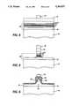
- FIG. 1is a cross-section of a substrate after deposition of a structural layer of amorphous silicon or polysilicon
- FIG. 2is a graph describing the dopant concentration in the structural layer of amorphous silicon or polysilicon shown in FIG. 1,
- FIG. 3is a cross-section of the substrate shown in FIG. 1 after nitride deposition
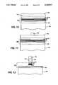
- FIG. 4is a cross-section of the substrate shown in FIG. 3 after photoresist patterning
- FIG. 5is a cross-section of the substrate shown in FIG. 4 after patterning the structural layer of amorphous silicon or polysilicon,
- FIG. 6is a cross-section of the substrate shown in FIG. 5 after oxidation
- FIG. 7is a cross-section of the substrate shown in FIG. 6 after oxide removal exposing the tip structure
- FIG. 8is a cross-section of a substrate after deposition of a structural layer of amorphous silicon or polysilicon
- FIG. 9is a graph describing the dopant concentration in the structural layer of amorphous silicon or polysilicon shown in FIG. 8,
- FIG. 10is a cross-section of the substrate shown in FIG. 8 after nitride deposition
- FIG. 11is a cross-section of the substrate shown in FIG. 10 after photoresist patterning
- FIG. 12is a cross-section of the substrate shown in FIG. 11 after patterning the structural layer of amorphous silicon or polysilicon,
- FIG. 13is a cross-section of the substrate shown in FIG. 12 after oxidation
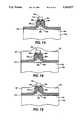
- FIG. 14is a cross-section of the substrate shown in FIG. 13 after photoresist deposition
- FIG. 15is a cross-section of the substrate shown in FIG. 14 after photoresist etch back
- FIG. 16is a cross-section of the substrate shown in FIG. 15 after metal deposition
- FIG. 17is a cross-section of the substrate shown in FIG. 16 after photoresist and oxide removal.
- the structureis produced on a substrate 10 as shown in FIG. 1. While silicon is convenient for the substrate 10 it is not necessary for the process.
- a 1.5-2.0 micron layer of amorphous silicon or polysilicon 12 with a surface 11is deposited on the substrate 10.
- the amorphous silicon or polysilicon 12will have a dopant concentration profile 14, as shown in FIGS. 1 and 2, that is highest at the surface 11 of the amorphous silicon or polysilicon 12.
- the dopant concentrationwill be the least at the amorphous silicon or polysilicon 12 interface 13 with the substrate 10. This dopant concentration can be accomplished in several ways, either by in situ doping or by ion implantation followed by diffusing. Both of these processes are well known and standard in the art.
- a nitride layer 16, 0.3-0.4 microns thick,has been deposited on the amorphous silicon or polysilicon 12. If it is desired to produce the dopant concentration profile 14 by ion implantation and annealing rather than by in situ doping the ion implantation and annealing steps may be done before the deposition of the nitride layer 16.
- the next stepis to pattern the nitride layer 16 and the amorphous silicon or polysilicon 12 by conventional photoresist processes.
- FIG. 5shows the nitride layer 16, and the amorphous silicon or polysilicon 12 etched using conventional dry etching techniques.
- the amorphous silicon or polysilicon 12will have tapered sidewalls due to the dopant concentration profile 14 in the amorphous silicon or polysilicon layer 12. The larger dopant concentration speeds up the etching process.
- the amorphous silicon or polysilicon 12is then oxidized to grow oxide bumpers 20 as shown in FIG. 6.
- the growth and control of oxide bumpersis discussed in U.S. Pat. No. 4,400,866 and 4,375,643 by Bol and Keming, both titled Application of Grown Oxide Bumper Insulators to a High Speed VLSI SASMEFET, incorporated by reference herein.
- the oxide bumperswill grow faster where the dopant concentration is the largest. Referring back to FIGS. 1 and 2, the dopant concentration is the largest at the surface 11 of the amorphous silicon or polysilicon 12.
- the oxide bumper 20will grow fastest and thickest near the surface 11 of the amorphous silicon or polysilicon 12.
- the nitride layer 16 on the surface 11 of the amorphous silicon or polysilicon 12will contribute to the shape of the oxide bumper 20. Since oxygen does not diffuse through nitride, no oxide will be grown on the nitride layer 16. The ability of oxygen to oxidize the amorphous silicon or polysilicon 12 will be reduced at the amorphous silicon or polysilicon 12 and nitride layer 16 interface 13 since the oxygen will have a reduced ability to diffuse along that interface due to protection of amorphous silicon or polysilicon 12 by the nitride layer 16. This phenomenon is very similar to the one responsible for the Bird's Beak formation in the CMOS or NMOS LOCOS processes. The oxidation rates will be fastest somewhat below the interface 13 and decrease with the decreasing dopant concentration.
- the oxide bumper 20grows, the remaining amorphous silicon or polysilicon 12 will form a tip structure 22 including the base 24 and the sharp point 26.
- the oxide bumper 20 and the amorphous silicon or polysilicon 12will form a partial or pseudo parabolic relationship in the example shown. Since oxidation rates are well known and easily controllable, the size and shape of the tip structure 22 can be precisely controlled.
- the final step, as shown in FIG. 7is removal of the oxide and nitride layers by well known conventional process steps leaving the fully formed tip structure 22 exposed.
- the amorphous silicon or polysilicon 12awill have a dopant concentration profile 14a, as shown in FIGS. 8 and 9, that is highest near the middle of the amorphous silicon or polysilicon 12a.
- the dopant concentrationwill be the least at the amorphous silicon or polysilicon 12 interface 13 with the substrate 10a and at the surface 11a of the amorphous silicon or polysilicon 12a.
- This dopant concentrationcan be accomplished in several ways, either by in situ doping or by ion implantation followed by annealing. Both of these processes are well known and standard in the art.
- a nitride layer 16ahas been deposited on the amorphous silicon or polysilicon 12a. If it is desired to produce the dopant concentration profile 14a by ion implantation and annealing rather, than by in situ doping, the ion implantation and annealing steps may be done before the deposition of the nitride layer 16a.
- FIG. 11shows the next step is to pattern layers 16 and 12 by conventional photoresist process.
- FIG. 12shows the nitride layer 16, and the amorphous silicon or polysilicon 12 etched using conventional dry etching techniques.
- the amorphous silicon or polysilicon 12awill have slightly concave sidewalls due to the dopant concentration profile 14a in the amorphous silicon or polysilicon 12a. The larger dopant concentration speeds up the etching process.
- the amorphous silicon or polysilicon 12ais then oxidized as shown in FIG. 13.
- the oxide bumperswill grow faster where the dopant concentration is the largest. Referring to FIGS. 8 and 9, the dopant concentration is the largest near the middle of the amorphous silicon or polysilicon 12a.
- the oxide bumper 20awill grow fastest and thickest near the middle of the amorphous silicon or polysilicon 12a.
- the oxidation rateswill be fastest near the middle of the amorphous silicon or polysilicon 12 and decrease with the decreasing dopant concentration.
- the remaining unoxidized amorphous silicon or polysilicon 12awill form a dual opposed tip structure 22a with two bases 24a and two sharp points 26a.
- the oxide bumper 20a and the amorphous silicon or polysilicon 12awill form a partial or pseudo hyperbolic relationship. Since oxidation rates are well known and easily controllable, the size and shape of the dual opposed tip structure 22a can be precisely controlled.
- a layer of planarizing photoresist 28is spun on the exposed surfaces. This is done to provide a method for attaching the upper tip to a lever arm.
- the photoresist 28is etched to reveal the nitride layer 16 on the base 24a of the upper tip. Then as shown in FIG. 16, first the nitride layer 16 is removed and a layer of metal 30 or other material is deposited on the surface of the photoresist 28 and the base 26a of the upper tip.
- the photoresist 28 and the oxide bumper 22acan be removed to expose the opposed tip pair 22a as is shown in FIG. 17.
Landscapes
- Engineering & Computer Science (AREA)
- Manufacturing & Machinery (AREA)
- Cold Cathode And The Manufacture (AREA)
- Local Oxidation Of Silicon (AREA)
Abstract
Description
Claims (13)
Priority Applications (4)
| Application Number | Priority Date | Filing Date | Title |
|---|---|---|---|
| US07/908,200US5269877A (en) | 1992-07-02 | 1992-07-02 | Field emission structure and method of forming same |
| JP14814593AJP3464500B2 (en) | 1992-07-02 | 1993-06-18 | Chip forming process |
| EP93305103AEP0578428B1 (en) | 1992-07-02 | 1993-06-29 | Method for making a field emission structure |
| DE69305258TDE69305258T2 (en) | 1992-07-02 | 1993-06-29 | Method of manufacturing a field emission device |
Applications Claiming Priority (1)
| Application Number | Priority Date | Filing Date | Title |
|---|---|---|---|
| US07/908,200US5269877A (en) | 1992-07-02 | 1992-07-02 | Field emission structure and method of forming same |
Publications (1)
| Publication Number | Publication Date |
|---|---|
| US5269877Atrue US5269877A (en) | 1993-12-14 |
Family
ID=25425354
Family Applications (1)
| Application Number | Title | Priority Date | Filing Date |
|---|---|---|---|
| US07/908,200Expired - LifetimeUS5269877A (en) | 1992-07-02 | 1992-07-02 | Field emission structure and method of forming same |
Country Status (4)
| Country | Link |
|---|---|
| US (1) | US5269877A (en) |
| EP (1) | EP0578428B1 (en) |
| JP (1) | JP3464500B2 (en) |
| DE (1) | DE69305258T2 (en) |
Cited By (6)
| Publication number | Priority date | Publication date | Assignee | Title |
|---|---|---|---|---|
| US5780347A (en)* | 1996-05-20 | 1998-07-14 | Kapoor; Ashok K. | Method of forming polysilicon local interconnects |
| US5923948A (en)* | 1994-11-04 | 1999-07-13 | Micron Technology, Inc. | Method for sharpening emitter sites using low temperature oxidation processes |
| US5981303A (en)* | 1994-09-16 | 1999-11-09 | Micron Technology, Inc. | Method of making field emitters with porous silicon |
| US6049089A (en)* | 1993-07-07 | 2000-04-11 | Micron Technology, Inc. | Electron emitters and method for forming them |
| JP3392507B2 (en) | 1994-03-23 | 2003-03-31 | 日本放送協会 | Small field emission cathode device |
| RU2414803C2 (en)* | 2007-12-14 | 2011-03-20 | Алексей Васильевич Савиных | Device for shaping uniform electric field in electroconductive medium |
Families Citing this family (3)
| Publication number | Priority date | Publication date | Assignee | Title |
|---|---|---|---|---|
| GB2378569B (en)* | 2001-08-11 | 2006-03-22 | Univ Dundee | Improved field emission backplate |
| GB2378570B (en)* | 2001-08-11 | 2005-11-16 | Univ Dundee | Improved field emission backplate |
| RU2332746C1 (en)* | 2006-12-25 | 2008-08-27 | Юрий Александрович Савиных | Method of uniform electric field generation in electroconductive medium |
Citations (2)
| Publication number | Priority date | Publication date | Assignee | Title |
|---|---|---|---|---|
| JPS5472959A (en)* | 1977-11-24 | 1979-06-11 | Hitachi Ltd | Formation method of electrode of semiconductor device |
| US4878900A (en)* | 1988-07-27 | 1989-11-07 | Sundt Thoralf M | Surgical probe and suction device |
Family Cites Families (1)
| Publication number | Priority date | Publication date | Assignee | Title |
|---|---|---|---|---|
| US4375643A (en)* | 1980-02-14 | 1983-03-01 | Xerox Corporation | Application of grown oxide bumper insulators to a high-speed VLSI SASMESFET |
- 1992
- 1992-07-02USUS07/908,200patent/US5269877A/ennot_activeExpired - Lifetime
- 1993
- 1993-06-18JPJP14814593Apatent/JP3464500B2/ennot_activeExpired - Fee Related
- 1993-06-29DEDE69305258Tpatent/DE69305258T2/ennot_activeExpired - Lifetime
- 1993-06-29EPEP93305103Apatent/EP0578428B1/ennot_activeExpired - Lifetime
Patent Citations (2)
| Publication number | Priority date | Publication date | Assignee | Title |
|---|---|---|---|---|
| JPS5472959A (en)* | 1977-11-24 | 1979-06-11 | Hitachi Ltd | Formation method of electrode of semiconductor device |
| US4878900A (en)* | 1988-07-27 | 1989-11-07 | Sundt Thoralf M | Surgical probe and suction device |
Non-Patent Citations (4)
| Title |
|---|
| Orvis, McConaghy, Ciarlo, Yee and Hee, "Modeling and Fabricating Micro-Cavity Integrated Vacuum Tubes", IEEE Transactions On Electron Devices, vol. 36, No. 11, Nov. 1989, pp. 2651-2657. |
| Orvis, McConaghy, Ciarlo, Yee and Hee, Modeling and Fabricating Micro Cavity Integrated Vacuum Tubes , IEEE Transactions On Electron Devices, vol. 36, No. 11, Nov. 1989, pp. 2651 2657.* |
| Yao, Arney, and MacDonald, "Fabrication of High Frequency Two-Dimensional Nanoactuators for Scanned Probe Devices", Journal of Microelectromechanical Systems, vol. 1, No. 1, Mar. 1992, pp. 14-21. |
| Yao, Arney, and MacDonald, Fabrication of High Frequency Two Dimensional Nanoactuators for Scanned Probe Devices , Journal of Microelectromechanical Systems, vol. 1, No. 1, Mar. 1992, pp. 14 21.* |
Cited By (16)
| Publication number | Priority date | Publication date | Assignee | Title |
|---|---|---|---|---|
| US6825596B1 (en) | 1993-07-07 | 2004-11-30 | Micron Technology, Inc. | Electron emitters with dopant gradient |
| US20070052339A1 (en)* | 1993-07-07 | 2007-03-08 | Cathey David A | Electron emitters with dopant gradient |
| US20060237812A1 (en)* | 1993-07-07 | 2006-10-26 | Cathey David A | Electronic emitters with dopant gradient |
| US6049089A (en)* | 1993-07-07 | 2000-04-11 | Micron Technology, Inc. | Electron emitters and method for forming them |
| US20060226765A1 (en)* | 1993-07-07 | 2006-10-12 | Cathey David A | Electronic emitters with dopant gradient |
| US7064476B2 (en) | 1993-07-07 | 2006-06-20 | Micron Technology, Inc. | Emitter |
| US20050023951A1 (en)* | 1993-07-07 | 2005-02-03 | Cathey David A. | Electron emitters with dopant gradient |
| JP3392507B2 (en) | 1994-03-23 | 2003-03-31 | 日本放送協会 | Small field emission cathode device |
| US6187604B1 (en) | 1994-09-16 | 2001-02-13 | Micron Technology, Inc. | Method of making field emitters using porous silicon |
| US6620640B2 (en) | 1994-09-16 | 2003-09-16 | Micron Technology, Inc. | Method of making field emitters |
| US6426234B2 (en) | 1994-09-16 | 2002-07-30 | Micron Technology, Inc. | Method of making field emitters using porous silicon |
| US5981303A (en)* | 1994-09-16 | 1999-11-09 | Micron Technology, Inc. | Method of making field emitters with porous silicon |
| US6312965B1 (en) | 1994-11-04 | 2001-11-06 | Micron Technology, Inc. | Method for sharpening emitter sites using low temperature oxidation process |
| US5923948A (en)* | 1994-11-04 | 1999-07-13 | Micron Technology, Inc. | Method for sharpening emitter sites using low temperature oxidation processes |
| US5780347A (en)* | 1996-05-20 | 1998-07-14 | Kapoor; Ashok K. | Method of forming polysilicon local interconnects |
| RU2414803C2 (en)* | 2007-12-14 | 2011-03-20 | Алексей Васильевич Савиных | Device for shaping uniform electric field in electroconductive medium |
Also Published As
| Publication number | Publication date |
|---|---|
| DE69305258T2 (en) | 1997-03-13 |
| EP0578428B1 (en) | 1996-10-09 |
| JP3464500B2 (en) | 2003-11-10 |
| JPH0689655A (en) | 1994-03-29 |
| DE69305258D1 (en) | 1996-11-14 |
| EP0578428A1 (en) | 1994-01-12 |
Similar Documents
| Publication | Publication Date | Title |
|---|---|---|
| US5066358A (en) | Nitride cantilevers with single crystal silicon tips | |
| US4407696A (en) | Fabrication of isolation oxidation for MOS circuit | |
| US6509139B1 (en) | Method of fabricating an integrated optical component | |
| EP0459397B1 (en) | Method of fabricating a semiconductor device having a trench for device isolation | |
| US5196367A (en) | Modified field isolation process with no channel-stop implant encroachment | |
| Wada | Ion‐Beam Etching of InP and Its Application to the Fabrication of High Radiance InGaAsP/InP Light Emitting Diodes | |
| JPH0650759B2 (en) | Method for making highly planarized integrated circuit structures | |
| US4900692A (en) | Method of forming an oxide liner and active area mask for selective epitaxial growth in an isolation trench | |
| US5269877A (en) | Field emission structure and method of forming same | |
| US5512509A (en) | Method for forming an isolation layer in a semiconductor device | |
| US4876216A (en) | Semiconductor integrated circuit manufacturing process providing oxide-filled trench isolation of circuit devices | |
| US5629230A (en) | Semiconductor processing method of forming field oxide regions on a semiconductor substrate utilizing a laterally outward projecting foot portion | |
| US4654119A (en) | Method for making submicron mask openings using sidewall and lift-off techniques | |
| US6713827B2 (en) | Micro-structures and methods for their manufacture | |
| US5858256A (en) | Method of forming small aperture | |
| JPH02304927A (en) | Manufacture of semiconductor device | |
| JP2896072B2 (en) | Method for forming field oxide film of semiconductor device | |
| GB2306780A (en) | Local oxidation of silicon method | |
| JPH05102292A (en) | Manufacture of isoplanar-separating type active region | |
| TWI269382B (en) | Method for manufacturing isolation structures in a semiconductor device | |
| US6979407B2 (en) | Process for producing an SPM sensor | |
| US5763316A (en) | Substrate isolation process to minimize junction leakage | |
| JPH02203549A (en) | Manufacturing method of semiconductor device | |
| KR100290901B1 (en) | Method for fabricating isolation film of semiconductor device | |
| KR0157921B1 (en) | Field oxide film manufacturing method |
Legal Events
| Date | Code | Title | Description |
|---|---|---|---|
| AS | Assignment | Owner name:XEROX CORPORATION, A CORP. OF NY, CONNECTICUT Free format text:ASSIGNMENT OF ASSIGNORS INTEREST.;ASSIGNOR:BOL, IGOR I.;REEL/FRAME:006181/0175 Effective date:19920629 | |
| STCF | Information on status: patent grant | Free format text:PATENTED CASE | |
| FEPP | Fee payment procedure | Free format text:PAYOR NUMBER ASSIGNED (ORIGINAL EVENT CODE: ASPN); ENTITY STATUS OF PATENT OWNER: LARGE ENTITY | |
| FPAY | Fee payment | Year of fee payment:4 | |
| FPAY | Fee payment | Year of fee payment:8 | |
| AS | Assignment | Owner name:BANK ONE, NA, AS ADMINISTRATIVE AGENT, ILLINOIS Free format text:SECURITY INTEREST;ASSIGNOR:XEROX CORPORATION;REEL/FRAME:013153/0001 Effective date:20020621 | |
| AS | Assignment | Owner name:JPMORGAN CHASE BANK, AS COLLATERAL AGENT, TEXAS Free format text:SECURITY AGREEMENT;ASSIGNOR:XEROX CORPORATION;REEL/FRAME:015134/0476 Effective date:20030625 Owner name:JPMORGAN CHASE BANK, AS COLLATERAL AGENT,TEXAS Free format text:SECURITY AGREEMENT;ASSIGNOR:XEROX CORPORATION;REEL/FRAME:015134/0476 Effective date:20030625 | |
| FPAY | Fee payment | Year of fee payment:12 | |
| AS | Assignment | Owner name:XEROX CORPORATION, CONNECTICUT Free format text:RELEASE BY SECURED PARTY;ASSIGNOR:JPMORGAN CHASE BANK, N.A. AS SUCCESSOR-IN-INTEREST ADMINISTRATIVE AGENT AND COLLATERAL AGENT TO JPMORGAN CHASE BANK;REEL/FRAME:066728/0193 Effective date:20220822 |