US5269847A - Variable rate distribution gas flow reaction chamber - Google Patents
Variable rate distribution gas flow reaction chamberDownload PDFInfo
- Publication number
- US5269847A US5269847AUS07/879,545US87954592AUS5269847AUS 5269847 AUS5269847 AUS 5269847AUS 87954592 AUS87954592 AUS 87954592AUS 5269847 AUS5269847 AUS 5269847A
- Authority
- US
- United States
- Prior art keywords
- wafer
- gas
- gases
- inlet port
- flow
- Prior art date
- Legal status (The legal status is an assumption and is not a legal conclusion. Google has not performed a legal analysis and makes no representation as to the accuracy of the status listed.)
- Expired - Lifetime
Links
Images


Classifications
- C—CHEMISTRY; METALLURGY
- C23—COATING METALLIC MATERIAL; COATING MATERIAL WITH METALLIC MATERIAL; CHEMICAL SURFACE TREATMENT; DIFFUSION TREATMENT OF METALLIC MATERIAL; COATING BY VACUUM EVAPORATION, BY SPUTTERING, BY ION IMPLANTATION OR BY CHEMICAL VAPOUR DEPOSITION, IN GENERAL; INHIBITING CORROSION OF METALLIC MATERIAL OR INCRUSTATION IN GENERAL
- C23C—COATING METALLIC MATERIAL; COATING MATERIAL WITH METALLIC MATERIAL; SURFACE TREATMENT OF METALLIC MATERIAL BY DIFFUSION INTO THE SURFACE, BY CHEMICAL CONVERSION OR SUBSTITUTION; COATING BY VACUUM EVAPORATION, BY SPUTTERING, BY ION IMPLANTATION OR BY CHEMICAL VAPOUR DEPOSITION, IN GENERAL
- C23C16/00—Chemical coating by decomposition of gaseous compounds, without leaving reaction products of surface material in the coating, i.e. chemical vapour deposition [CVD] processes
- C23C16/44—Chemical coating by decomposition of gaseous compounds, without leaving reaction products of surface material in the coating, i.e. chemical vapour deposition [CVD] processes characterised by the method of coating
- C23C16/455—Chemical coating by decomposition of gaseous compounds, without leaving reaction products of surface material in the coating, i.e. chemical vapour deposition [CVD] processes characterised by the method of coating characterised by the method used for introducing gases into reaction chamber or for modifying gas flows in reaction chamber
- Y—GENERAL TAGGING OF NEW TECHNOLOGICAL DEVELOPMENTS; GENERAL TAGGING OF CROSS-SECTIONAL TECHNOLOGIES SPANNING OVER SEVERAL SECTIONS OF THE IPC; TECHNICAL SUBJECTS COVERED BY FORMER USPC CROSS-REFERENCE ART COLLECTIONS [XRACs] AND DIGESTS
- Y10—TECHNICAL SUBJECTS COVERED BY FORMER USPC
- Y10S—TECHNICAL SUBJECTS COVERED BY FORMER USPC CROSS-REFERENCE ART COLLECTIONS [XRACs] AND DIGESTS
- Y10S438/00—Semiconductor device manufacturing: process
- Y10S438/935—Gas flow control
Definitions
- This inventionrelates in general to reaction chambers and relates more particularly to the supply of reactant gases to such chambers.
- each element indicated by a reference numeralwill be indicated by the same reference numeral in every figure in which that element appears.
- the first digit of any two or three digit reference numeralsindicates the first figure in which its associated element is presented.
- process gasesare injected into the processing chamber at a point that is remote from the wafer so that a uniform distribution of the gases is achieved before these gases reach the wafer.
- the waferis typically located between the remote gas inlets and an exhaust port so that the reactant gases flow past the wafer.
- a gas flow systemthat enables accurate control of gas flow rates and composition across a wafer during processing, thereby enhancing the ability to control the distribution of wafer processing rates across the wafer.
- This gas flow systemis applicable to batch processing systems, it is best implemented in single wafer processing systems.
- This gas flow systemprovides the process gases from a gas inlet port adjacent to the wafer(s) so that the flow rates and concentrations of the gases at the wafer can be more accurately controlled.
- the gasesare applied near the edge of the wafer at one side of the wafer and flow across the wafer to an exhaust port located diametrically opposite across the wafer from the gas inlet port.
- the spacing between the gas inlet port and the nearest edge of the wafer as well as the spacing between the exhaust port and the nearest edge of the waferare small so that there is a reduced amount of deadspace in the system and so that control of the distribution of gases across the wafer is enhanced.
- the reactorit is advantageous for the reactor to include a cylindrical section that closely surrounds the sides of the wafer. The inlet port and exhaust port can be located in this cylindrical section to enable them to inject and exhaust, respectively, gases at the wafer.
- a gas supply manifoldis attached to the gas inlet port to enable the gas composition and flow rate to be varied across the gas inlet port, thereby enabling control over the spatial distribution of gas composition and flow rates at the wafer surface.
- This gas supply manifoldincludes a set of gas injectors each of which is connected through flow controllers to associated gas sources.
- the gas inlet portis preferably in the shape of a thin slot that is parallel to the wafer so that this port supplies gases to the immediate vicinity of the edge of the wafer.
- the exhaust portis also preferably in the shape of a thin exit slit that is parallel to the wafer so that this port exhausts gases from the immediate vicinity of the edge of the wafer.
- a number of vertical vanescan be included to provide physical strengthening of the inlet port.
- these vanescan prevent mixing of injected gases from different inlet jets of the gas supply manifold until these gases reach points closer to the edge of the wafer than the distance of the gas injectors from the edge of the wafer.
- Each pair of adjacent vanesdefines the sides of a gas transport channel that prevents mixing of gases between different channels.
- the gas inlet portnarrows into a narrow inlet slit that is slightly wider than the diameter of wafers to be processed in this processing system. This enables some local mixing of the gases before these gases reach the vicinity of the wafer. This smooths the concentration and flow profiles of the inlet gases before they reach the wafer and yet enables a nonconstant concentration and flow profile to be achieved across the wafer.
- a preheat susceptor ringcan be included between the inlet slit and the wafer to preheat the injected gases before they reach the wafer.
- This ringpreferably extends completely around the wafer so that it provides a symmetric temperature environment for the wafer.
- the susceptoris selected to be of a material that is opaque to this light. It is also advantageous for this material to have a low thermal mass so that the temperature can be rapidly changed by the light sources.
- the waferis rotated to produce a temporally averaged, radially symmetric processing of the wafer even though the gas flow and/or concentration is not constant across the wafer.
- FIG. 1is a side view of a wafer processing reactor in accordance with the present invention.
- FIG. 2is a top cross-sectional view of the wafer processing reactor of FIG. 1 illustrating an array of heating lamps utilized to heat the wafer.
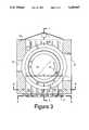
- FIG. 3is a top cross-sectional view of the wafer processing reactor of FIG. 1 through a plane containing a gas inlet port and a gas exhaust port.
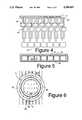
- FIG. 4is a side view of the gas supply manifold, as indicated in FIG. 3.
- FIG. 5is a side view cross-section of the gas inlet port, as indicated in FIG. 3.
- FIG. 6illustrates flow stramlines of gas from the gas inlet port to the gas outlet port.
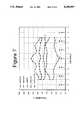
- FIG. 7presents empirical plots of deposition thickness on a wafer as a function of wafer radius for several selections of gas flow rates into 7 different gas transport channels.
- FIG. 1is a side view of a wafer processing reactor in accordance with the present invention.
- Walls 11-13enclose a reaction chamber 14 in which processing of wafers takes place.
- a wafer pedestal 15 within this chambercan be rotated to produce axially symmetric processing of wafers by producing a time-averaged environment for a wafer 16 that is centered on the rotation axis.
- Wafer 16is heated by means of an array of lamps 17 that are distributed in a ring centered on an axis that passes perpendicularly through wafer 16. A top cross-sectional view of these lamps is presented in FIG. 2.
- the wafer pedestalis preferably of an opaque material that can withstand the processing temperatures so that light from lamps 17 heats the wafer even if the wafer is transparent to the light from lamps 17.
- the pedestalis silicon carbide coated graphite.
- arrays of lamps 17are included both above and below pedestal 15.
- walls 11 and 13are transparent to the light from these lamps.
- a convenient choice of material for these wallsis quartz because of its transparency, strength (to withstand pressure differences across these walls) and ability to withstand the elevated temperatures (typically 500-1,200 degrees Centigrade) utilized during wafer processing. Typical process pressures can be as low as a few Torr so that these walls need to withstand a full atmosphere of pressure.
- Sidewall 12is typically a machined block of material such as quartz. In other applications, such as other CVD or etching processes, suitable choices of material include aluminum and stainless steel.
- Additional gasessuch as hydrogen or nitrogen can be injected through a gas inlet 19 into reaction chamber 14 to prevent the reactant gases from flowing into the bottom half of the process chamber.
- a set of infrared detectors 110are utilized to measure the wafer temperature and provide a feedback to a power source for lamps 17 to regulate the wafer temperature.
- a reactor of this typeis illustrated in greater detail in copending patent application Ser. No. 07/491,416 entitled Double-Dome Reactor For Semiconductor Processing filed by Roger N. Anderson, et al on Mar. 9, 1990.
- FIG. 3is a top cross-sectional view of the wafer processing reactor of FIG. 1 through a plane containing a gas inlet port 31 and a gas exhaust port 32.
- a hole 33is included for use by various pieces of equipment such as a thermocouple to measure the gas temperature within reaction chamber 14.
- a slot 34enables wafers to be transmitted into and out of the reaction chamber.
- Arrow 35illustrates that pedestal 15 and wafer 16 are rotated about an axis A that is substantially centered on the wafer and is substantially perpendicular to a top surface of the wafer.
- a preheat ring susceptor 36is included to provide heating of injected gases before they reach the wafer.
- This preheat ring susceptor 36is opaque to the light from lamps 17 and, in this embodiment, is silicon carbide coated graphite. Reactant and carrier gases are supplied into gas inlet port 31 by a gas supply manifold 37 that is illustrated in greater detail in FIG. 4.
- the gas supply manifold 37supplies only a pair of different gases.
- a first of these gasesis supplied from a first gas source to a first pipe 41 and a second of these gases is supplied from a second gas source to a second pipe 43.
- Each of these two pipessplits into seven pipes, each provided at one of a set of inlets 310 to a different channel 51 (illustrated in FIG. 5 and discussed below in regard to that figure) of the gas inlet port 31.
- Between pipe 41 and each of the seven pipes from it to the gas inlet port channelsis an associated flow controller 42.
- pipe 43 and each of the seven pipes from it to the gas inlet port channelsis an associated flow controller 44. This enables the flow rate of each of these two gases to each of the seven channels to be independently controlled.
- the concentrations in the channelsare then determined by the mix of these two gases in these channels and by the concentrations of these two gases.
- more than two pipessuch as 41 and 43 can be provided to enable more control over the gas flow and concentration.
- various carrier gases as well as multiple reactant gasescan be provided.
- fewer or greater than 7 channelscan be utilized to distribute these gases.
- FIG. 5is a side view cross-section of the gas inlet port 31.
- a set of vanes 38extend from a bottom wall 52 to a top wall 53 of the gas inlet port and provides support for the gas inlet port. These vanes also divide the gas inlet port into a set of seven channels 51 that provide the ability to prevent mixing of injected gases until a point closer to the edge of the wafer being processed. This enables greater control over and flow and concentration profiles of reactant and carrier gases across the top surface of the wafer.
- a typical flow profileis illustrated in FIG. 6 by dashed lines 61 that indicate boundary lines between the gas flow from adjacent channels 51. This flow profile can be altered by altering the total gas flow through each of these seven channels 51. The reaction process can also be altered by changing the relative mix of gases through each of these channels.
- a thin slit 39through which the reactant and carrier gases pass before entering the reactor chamber. Because the vanes do not extend into this region, the gases from adjacent channels can begin to mix, thereby smoothing out the concentration and flow profiles before these gases reach the vicinity of the wafer.
- This narrow slithas a width W as wide as the width of the gas inlet port 31 within the region containing the vanes.
- the heighti.e., the dimension of this slit perpendicular to the view of FIG. 3
- a greater flux of reactantsis required in the middle channels so that a relatively higher flux results near the center of the wafer than at the perimeter.
- This higher fluxis required in these channels because the concentration is partially depleted as it passes over the peripheral region of the wafer and on to the central portion.
- the peripheral regions of the waferinteract not only with the gas from the inner channels, but also interact within regions 63 and 64 with gases supplied through the outer channels.
- This figurerepresents the process of silicon deposition and displays the thickness (in microns), as a function of radial distance from the center of the wafer, of the resulting layer produced on the wafer.
- the total flow rate within each of the seven channelsIn the top left corner is indicated the total flow rate within each of the seven channels. Only four numbers are indicated since a symmetric pattern of relative flow rates is utilized in these tests.
- the first and seventh channelsi.e., the outermost channels
- the second and sixth channelsi.e., the 2nd outermost channels
- the third and fifth channelshave a flow rate of 4.5
- the fourth channeli.e., the central channel
- the total flow rate through gas inlet 19is on the order of 8 liters per minute and the total flow rate through gas inlet port is on the order of 20-30 liters per minute.
- Optimal uniformity for the process of silicon depositionwas achieved for relative flow rates of 11, 9, 10, 10, 10, 9, and 11 in channels 1-7, respectively. This choice produces a better uniformity than when all of these flow rates are equal.
- Micrometering valves and fixed orificesare utilized as flow controllers 42 and 44 to control flow rate.
- Other devices for controlling flow ratesinclude mass flow controllers or other variable restrictors.
- vanes 38are all parallel and are directed straight ahead as can be seen in FIGS. 3 and 6.
- the directions of these vanescan also be an adjustable process parameter.
- Vanescan also be placed in the slit area 39 of the inlet or the exhaust 311 to alter the flow pattern. Other variations include changes in the flow channel width W relative to the other dimensions or altering the number of flow channels used in the inlet independent of the number used in the exhaust.
Landscapes
- Chemical & Material Sciences (AREA)
- General Chemical & Material Sciences (AREA)
- Chemical Kinetics & Catalysis (AREA)
- Engineering & Computer Science (AREA)
- Materials Engineering (AREA)
- Mechanical Engineering (AREA)
- Metallurgy (AREA)
- Organic Chemistry (AREA)
- Chemical Vapour Deposition (AREA)
Abstract
Description
This is a continuation of U.S. application Ser. No. 07/571,957 filed Aug. 23, 1990; now abandoned.
This invention relates in general to reaction chambers and relates more particularly to the supply of reactant gases to such chambers.
In the figures, each element indicated by a reference numeral will be indicated by the same reference numeral in every figure in which that element appears. The first digit of any two or three digit reference numerals indicates the first figure in which its associated element is presented.
To remain price competitive in integrated circuit fabrication it is important to increase continually the throughput of a wafer processing system. Batch processing systems have been used to increase throughput. However, in state of the art devices it is necessary to utilize single wafer processing systems to achieve the processing uniformity needed to achieve state of the art feature sizes. For equipment utilized to achieve state of the art linewidths it is particularly important to achieve as high a uniformity of processing across the wafer as possible.
As the feature size of integrated circuits shrinks and the size of wafers increases, it becomes increasingly important to accurately control the rates of various wafer processing steps to achieve process uniformity across the entire wafer. The uniformity obtained by all process steps, including all plasma processes and chemical vapor deposition processes, are affected by the distribution of process gases within the processing chamber. In many existing systems, process gases are injected into the processing chamber at a point that is remote from the wafer so that a uniform distribution of the gases is achieved before these gases reach the wafer. The wafer is typically located between the remote gas inlets and an exhaust port so that the reactant gases flow past the wafer. To further improve the uniformity of processing, many systems include the ability to rotate the wafer during processing to increase the uniformity of the time-averaged physical and chemical environment of the wafer during processing. However, to achieve improved process control it would be advantageous to have a greater degree of control over the distribution of gases within the reaction chamber than is now available.
In accordance with the illustrated preferred embodiment, a gas flow system is presented that enables accurate control of gas flow rates and composition across a wafer during processing, thereby enhancing the ability to control the distribution of wafer processing rates across the wafer. Although this gas flow system is applicable to batch processing systems, it is best implemented in single wafer processing systems. This gas flow system provides the process gases from a gas inlet port adjacent to the wafer(s) so that the flow rates and concentrations of the gases at the wafer can be more accurately controlled. Preferably, the gases are applied near the edge of the wafer at one side of the wafer and flow across the wafer to an exhaust port located diametrically opposite across the wafer from the gas inlet port. Preferably, the spacing between the gas inlet port and the nearest edge of the wafer as well as the spacing between the exhaust port and the nearest edge of the wafer are small so that there is a reduced amount of deadspace in the system and so that control of the distribution of gases across the wafer is enhanced. Thus, it is advantageous for the reactor to include a cylindrical section that closely surrounds the sides of the wafer. The inlet port and exhaust port can be located in this cylindrical section to enable them to inject and exhaust, respectively, gases at the wafer.
A gas supply manifold is attached to the gas inlet port to enable the gas composition and flow rate to be varied across the gas inlet port, thereby enabling control over the spatial distribution of gas composition and flow rates at the wafer surface. This gas supply manifold includes a set of gas injectors each of which is connected through flow controllers to associated gas sources. The gas inlet port is preferably in the shape of a thin slot that is parallel to the wafer so that this port supplies gases to the immediate vicinity of the edge of the wafer. The exhaust port is also preferably in the shape of a thin exit slit that is parallel to the wafer so that this port exhausts gases from the immediate vicinity of the edge of the wafer.
In the gas inlet port, a number of vertical vanes can be included to provide physical strengthening of the inlet port. In addition, these vanes can prevent mixing of injected gases from different inlet jets of the gas supply manifold until these gases reach points closer to the edge of the wafer than the distance of the gas injectors from the edge of the wafer. Each pair of adjacent vanes defines the sides of a gas transport channel that prevents mixing of gases between different channels. Typically, there will be as many different gas transport channels as there are inlet gas injectors. At the inner ends of these channels, the gas inlet port narrows into a narrow inlet slit that is slightly wider than the diameter of wafers to be processed in this processing system. This enables some local mixing of the gases before these gases reach the vicinity of the wafer. This smooths the concentration and flow profiles of the inlet gases before they reach the wafer and yet enables a nonconstant concentration and flow profile to be achieved across the wafer.
A preheat susceptor ring can be included between the inlet slit and the wafer to preheat the injected gases before they reach the wafer. This ring preferably extends completely around the wafer so that it provides a symmetric temperature environment for the wafer. In a processing system in which elevated process temperatures are produced by intense light from a light source, the susceptor is selected to be of a material that is opaque to this light. It is also advantageous for this material to have a low thermal mass so that the temperature can be rapidly changed by the light sources.
If the gas flow and concentration profiles are constant across the gas inlet port, then an increased process rate results at the perimeter of the wafer. This occurs because the reactant concentrations are depleted as they flow across the wafer to process the wafer. This is particularly easy to see for the case in which a portion of these reactant gases deposit on the wafer, but it is also true for other processes, such as etching processes in which the reactant gases are used up during that process step. Therefore, in general, it is advantageous to have a greater concentration and/or a greater flow rate for the portion of the reactant gas stream that crosses near the center of the wafer. Preferably, the wafer is rotated to produce a temporally averaged, radially symmetric processing of the wafer even though the gas flow and/or concentration is not constant across the wafer.
Although the gas flow rate and wafer rotation rate are low enough that there will generally be nonturbulent gas flow within the reactor chamber, the complicated interaction between the various parameters limits the ability to accurately determine theoretically the desired flow and concentration profiles. This is particularly true in most preferred embodiments of reactors because of the complicated interaction between heating effects, rotation of the wafer, flow rates, concentrations, backflow of gases in the rotating wafer system, temperature decomposition of the gases and complex reactions between the reactant gases and the wafer. Such theoretical analysis can be a starting point, but optimization is generally achieved empirically.
FIG. 1 is a side view of a wafer processing reactor in accordance with the present invention.
FIG. 2 is a top cross-sectional view of the wafer processing reactor of FIG. 1 illustrating an array of heating lamps utilized to heat the wafer.
FIG. 3 is a top cross-sectional view of the wafer processing reactor of FIG. 1 through a plane containing a gas inlet port and a gas exhaust port.
FIG. 4 is a side view of the gas supply manifold, as indicated in FIG. 3.
FIG. 5 is a side view cross-section of the gas inlet port, as indicated in FIG. 3.
FIG. 6 illustrates flow stramlines of gas from the gas inlet port to the gas outlet port.
FIG. 7 presents empirical plots of deposition thickness on a wafer as a function of wafer radius for several selections of gas flow rates into 7 different gas transport channels.
FIG. 1 is a side view of a wafer processing reactor in accordance with the present invention. Walls 11-13 enclose areaction chamber 14 in which processing of wafers takes place. Awafer pedestal 15 within this chamber can be rotated to produce axially symmetric processing of wafers by producing a time-averaged environment for awafer 16 that is centered on the rotation axis.
Wafer 16 is heated by means of an array oflamps 17 that are distributed in a ring centered on an axis that passes perpendicularly throughwafer 16. A top cross-sectional view of these lamps is presented in FIG. 2. The wafer pedestal is preferably of an opaque material that can withstand the processing temperatures so that light fromlamps 17 heats the wafer even if the wafer is transparent to the light fromlamps 17. In this embodiment, the pedestal is silicon carbide coated graphite.
To increase the rate at which the wafer can be thermally cycled, arrays oflamps 17 are included both above and belowpedestal 15. To enable this light to reach the pedestal,walls Sidewall 12 is typically a machined block of material such as quartz. In other applications, such as other CVD or etching processes, suitable choices of material include aluminum and stainless steel. Additional gases such as hydrogen or nitrogen can be injected through agas inlet 19 intoreaction chamber 14 to prevent the reactant gases from flowing into the bottom half of the process chamber. A set ofinfrared detectors 110 are utilized to measure the wafer temperature and provide a feedback to a power source forlamps 17 to regulate the wafer temperature. A reactor of this type is illustrated in greater detail in copending patent application Ser. No. 07/491,416 entitled Double-Dome Reactor For Semiconductor Processing filed by Roger N. Anderson, et al on Mar. 9, 1990.
FIG. 3 is a top cross-sectional view of the wafer processing reactor of FIG. 1 through a plane containing agas inlet port 31 and agas exhaust port 32. Ahole 33 is included for use by various pieces of equipment such as a thermocouple to measure the gas temperature withinreaction chamber 14. Aslot 34 enables wafers to be transmitted into and out of the reaction chamber.Arrow 35 illustrates thatpedestal 15 andwafer 16 are rotated about an axis A that is substantially centered on the wafer and is substantially perpendicular to a top surface of the wafer. Apreheat ring susceptor 36 is included to provide heating of injected gases before they reach the wafer. Although this can be achieved by a preheat susceptor that does not encircle the wafer, it is advantageous to encircle the wafer so that it experiences a more uniform processing environment. Thispreheat ring susceptor 36 is opaque to the light fromlamps 17 and, in this embodiment, is silicon carbide coated graphite. Reactant and carrier gases are supplied intogas inlet port 31 by agas supply manifold 37 that is illustrated in greater detail in FIG. 4.
In this embodiment thegas supply manifold 37 supplies only a pair of different gases. A first of these gases is supplied from a first gas source to afirst pipe 41 and a second of these gases is supplied from a second gas source to asecond pipe 43. Each of these two pipes splits into seven pipes, each provided at one of a set ofinlets 310 to a different channel 51 (illustrated in FIG. 5 and discussed below in regard to that figure) of thegas inlet port 31. Betweenpipe 41 and each of the seven pipes from it to the gas inlet port channels is an associatedflow controller 42. Similarly, betweenpipe 43 and each of the seven pipes from it to the gas inlet port channels is an associatedflow controller 44. This enables the flow rate of each of these two gases to each of the seven channels to be independently controlled. The concentrations in the channels are then determined by the mix of these two gases in these channels and by the concentrations of these two gases. In other embodiments more than two pipes such as 41 and 43 can be provided to enable more control over the gas flow and concentration. For example, various carrier gases as well as multiple reactant gases can be provided. Also, fewer or greater than 7 channels can be utilized to distribute these gases.
FIG. 5 is a side view cross-section of thegas inlet port 31. A set ofvanes 38 extend from abottom wall 52 to atop wall 53 of the gas inlet port and provides support for the gas inlet port. These vanes also divide the gas inlet port into a set of sevenchannels 51 that provide the ability to prevent mixing of injected gases until a point closer to the edge of the wafer being processed. This enables greater control over and flow and concentration profiles of reactant and carrier gases across the top surface of the wafer. A typical flow profile is illustrated in FIG. 6 by dashedlines 61 that indicate boundary lines between the gas flow fromadjacent channels 51. This flow profile can be altered by altering the total gas flow through each of these sevenchannels 51. The reaction process can also be altered by changing the relative mix of gases through each of these channels.
As is illustrated in FIG. 3, between the ends of thevanes 38 and the wafer is athin slit 39 through which the reactant and carrier gases pass before entering the reactor chamber. Because the vanes do not extend into this region, the gases from adjacent channels can begin to mix, thereby smoothing out the concentration and flow profiles before these gases reach the vicinity of the wafer. This narrow slit has a width W as wide as the width of thegas inlet port 31 within the region containing the vanes. The height (i.e., the dimension of this slit perpendicular to the view of FIG. 3) is on the order of 3 mm so that the gases are injected into a region of small height at the wafer edge. This produces an efficient utilization of the reactant gases because this thin region will tend to flow uniformly across the reaction chamber to the exhaust port.
In general, a greater flux of reactants is required in the middle channels so that a relatively higher flux results near the center of the wafer than at the perimeter. This higher flux is required in these channels because the concentration is partially depleted as it passes over the peripheral region of the wafer and on to the central portion. Furthermore, the peripheral regions of the wafer interact not only with the gas from the inner channels, but also interact withinregions
The complicated interaction between heating effects, rotation of the wafer, flow rates, concentrations, backflow of gases in the rotating wafer system, temperature, decomposition of the gases, thermal convection and complex reactions between the reactant gases and the wafer make it extremely difficult to accurately predict what combination of flow rates and concentrations will be optimal, so theoretical considerations will generally be only a starting point for the selection of the gas flow rates and concentrations through each of the channels. Because the wafer surface is heated by light fromlamps 17, local convection cells can dominate flow patterns. Empirical measurements will almost always be required to optimize the process. FIG. 7 illustrates a typical set of such empirical data.
This figure represents the process of silicon deposition and displays the thickness (in microns), as a function of radial distance from the center of the wafer, of the resulting layer produced on the wafer. In the top left corner is indicated the total flow rate within each of the seven channels. Only four numbers are indicated since a symmetric pattern of relative flow rates is utilized in these tests. Thus, for the top curve, the first and seventh channels (i.e., the outermost channels) have zero gas flow, the second and sixth channels (i.e., the 2nd outermost channels) have a flow rate of 4, the third and fifth channels have a flow rate of 4.5 and the fourth channel (i.e., the central channel) has a flow rate of 5. This plot shows that the expected result that the first and seventh channels have a strong effect on the deposition over the outer regions of the wafer. Somewhat surprisingly, the third and fourth of these curves show that the flow in the third and fifth channels has a greater effect on the thickness at the center of the wafer than does the flow rate in the central channel.
In a typical process, the total flow rate throughgas inlet 19 is on the order of 8 liters per minute and the total flow rate through gas inlet port is on the order of 20-30 liters per minute. Optimal uniformity for the process of silicon deposition was achieved for relative flow rates of 11, 9, 10, 10, 10, 9, and 11 in channels 1-7, respectively. This choice produces a better uniformity than when all of these flow rates are equal. Micrometering valves and fixed orifices are utilized asflow controllers
In the embodiment of FIGS. 1-6,vanes 38 are all parallel and are directed straight ahead as can be seen in FIGS. 3 and 6. In alternate embodiments, the directions of these vanes can also be an adjustable process parameter. Vanes can also be placed in theslit area 39 of the inlet or theexhaust 311 to alter the flow pattern. Other variations include changes in the flow channel width W relative to the other dimensions or altering the number of flow channels used in the inlet independent of the number used in the exhaust.
Claims (11)
1. Wafer processing reactor comprising:
reactor chamber walls that enclose a reaction chamber within which wafers are to be processed;
a gas inlet port for supplying at least one process gas into said reaction chamber adjacent an edge of said wafer in a plane parallel to said wafer, said gas inlet port having a width slightly wider than the diameter of the wafer; and
a gas supply manifold that injects at least one process gas through a plurality of spatially separated inlets into said gas inlet port, each of said inlets having a means of separate flow control in flow path from a source of process gas to one of said inlets, thereby providing an ability to control a gas flow spatial distribution of said at least one process gas through said gas inlet port.
2. Wafer processing reactor as in claim 1 wherein at least two different process gases are injected through inlets adjacent an edge of said wafer, thereby enabling control over the distribution of gas composition as well as flow rate.
3. Wafer processing reactor as in claim 1 wherein said wafer is rotated during processing.
4. Wafer processing reactor as in claim 1 wherein said side wall portion of said walls includes a cylindrical section that encircles a circular region within which a wafer is to be located for processing and across which said at least one process gas flows.
5. Wafer processing reactor as in claim 1 wherein each of said flow controllers are selected from the set consisting of mass flow controllers, fixed orifices and micrometer valves.
6. Wafer processing reactor as in claim 1 wherein each of said inlets can be connected to at least two different sources of process gas, whereby a total flow rate and a relative concentration of process gases can be controlled through each of said inlets.
7. Wafer processing reactor as in claim 1 wherein gas flow is adjusted to be higher near the center of a wafer being processed than near the periphery of said wafer.
8. Wafer processing reactor comprising:
reactor chamber walls that enclose a reaction chamber within which wafers are to be processed;
a gas inlet port for supplying at least one process gas into said reaction chamber, and, within said gas inlet port
a plurality of vanes that separate this gas inlet port into a plurality of gas flow channels, whereby mixing of gases injected through different inlets can be delayed until process gases through these different inlets reach a distal end of these vanes, and
a gas supply manifold that injects at least one process gas to a plurality of spatially separated inlets to said gas inlet port, thereby providing an ability to control a gas flow distribution of said at least one process gas through said gas inlet port.
9. Wafer processing reactor as in claim 8 wherein said vanes are all parallel.
10. Wafer processing reactor as in claim 8 further comprising:
wherein a side wall portion of said reactor walls has formed therethrough a slit, located between a distal end of said vanes and said process chamber, within which process gases from different channels can begin to mix before reaching a location at which a wafer is to be located for processing, thereby smoothing a flow rate profile of gases passing through said channels before these gases reach said location at which a wafer is to be located for processing.
11. Wafer processing reactor as in claim 8 wherein said vanes are not all parallel.
Priority Applications (2)
| Application Number | Priority Date | Filing Date | Title |
|---|---|---|---|
| US07/879,545US5269847A (en) | 1990-08-23 | 1992-05-04 | Variable rate distribution gas flow reaction chamber |
| US08/122,270US5455070A (en) | 1990-08-23 | 1993-09-16 | Variable rate distribution gas flow reaction chamber |
Applications Claiming Priority (2)
| Application Number | Priority Date | Filing Date | Title |
|---|---|---|---|
| US57195790A | 1990-08-23 | 1990-08-23 | |
| US07/879,545US5269847A (en) | 1990-08-23 | 1992-05-04 | Variable rate distribution gas flow reaction chamber |
Related Parent Applications (1)
| Application Number | Title | Priority Date | Filing Date |
|---|---|---|---|
| US57195790AContinuation | 1990-08-23 | 1990-08-23 |
Related Child Applications (1)
| Application Number | Title | Priority Date | Filing Date |
|---|---|---|---|
| US08/122,270DivisionUS5455070A (en) | 1990-08-23 | 1993-09-16 | Variable rate distribution gas flow reaction chamber |
Publications (1)
| Publication Number | Publication Date |
|---|---|
| US5269847Atrue US5269847A (en) | 1993-12-14 |
Family
ID=27075691
Family Applications (2)
| Application Number | Title | Priority Date | Filing Date |
|---|---|---|---|
| US07/879,545Expired - LifetimeUS5269847A (en) | 1990-08-23 | 1992-05-04 | Variable rate distribution gas flow reaction chamber |
| US08/122,270Expired - LifetimeUS5455070A (en) | 1990-08-23 | 1993-09-16 | Variable rate distribution gas flow reaction chamber |
Family Applications After (1)
| Application Number | Title | Priority Date | Filing Date |
|---|---|---|---|
| US08/122,270Expired - LifetimeUS5455070A (en) | 1990-08-23 | 1993-09-16 | Variable rate distribution gas flow reaction chamber |
Country Status (1)
| Country | Link |
|---|---|
| US (2) | US5269847A (en) |
Cited By (92)
| Publication number | Priority date | Publication date | Assignee | Title |
|---|---|---|---|---|
| US5439523A (en)* | 1994-02-14 | 1995-08-08 | Memc Electronic Materials, Inc. | Device for suppressing particle splash onto a semiconductor wafer |
| US5451258A (en)* | 1994-05-11 | 1995-09-19 | Materials Research Corporation | Apparatus and method for improved delivery of vaporized reactant gases to a reaction chamber |
| WO1995033082A3 (en)* | 1994-05-26 | 1996-01-11 | Philips Electronics Nv | Plasma treatment and apparatus in electronic device manufacture |
| US5522934A (en)* | 1994-04-26 | 1996-06-04 | Tokyo Electron Limited | Plasma processing apparatus using vertical gas inlets one on top of another |
| US5525157A (en)* | 1987-06-24 | 1996-06-11 | Advanced Semiconductor Materials America, Inc. | Gas injectors for reaction chambers in CVD systems |
| US5551985A (en)* | 1995-08-18 | 1996-09-03 | Torrex Equipment Corporation | Method and apparatus for cold wall chemical vapor deposition |
| US5551982A (en)* | 1994-03-31 | 1996-09-03 | Applied Materials, Inc. | Semiconductor wafer process chamber with susceptor back coating |
| US5576059A (en)* | 1993-01-13 | 1996-11-19 | Applied Materials, Inc. | Depositing polysilicon films having improved uniformity and apparatus therefor |
| US5645646A (en)* | 1994-02-25 | 1997-07-08 | Applied Materials, Inc. | Susceptor for deposition apparatus |
| US5653808A (en)* | 1996-08-07 | 1997-08-05 | Macleish; Joseph H. | Gas injection system for CVD reactors |
| US5679165A (en)* | 1992-11-30 | 1997-10-21 | Semiconductor Process Laboratory Co., Ltd. | Apparatus for manufacturing semiconductor device |
| US5683548A (en)* | 1996-02-22 | 1997-11-04 | Motorola, Inc. | Inductively coupled plasma reactor and process |
| US5693238A (en)* | 1993-05-03 | 1997-12-02 | Balzers Aktiengesellschaft | Method for improving the rate of a plasma enhanced vacuum treatment |
| US5704982A (en)* | 1994-09-27 | 1998-01-06 | Saint-Gobain Vitrage | Technique for depositing coatings by pyrolysis/decomposition of precursor gas or gases |
| US5755886A (en)* | 1986-12-19 | 1998-05-26 | Applied Materials, Inc. | Apparatus for preventing deposition gases from contacting a selected region of a substrate during deposition processing |
| US5853484A (en)* | 1995-10-28 | 1998-12-29 | Lg Semicon Co., Ltd. | Gas distribution system and method for chemical vapor deposition apparatus |
| US5853485A (en)* | 1994-11-16 | 1998-12-29 | The B. F. Goodrich Company | Pressure gradient CVI/CVD apparatus process and product |
| US5891250A (en)* | 1998-05-05 | 1999-04-06 | Memc Electronic Materials, Inc. | Injector for reactor |
| US5895530A (en)* | 1996-02-26 | 1999-04-20 | Applied Materials, Inc. | Method and apparatus for directing fluid through a semiconductor processing chamber |
| US5916369A (en)* | 1995-06-07 | 1999-06-29 | Applied Materials, Inc. | Gas inlets for wafer processing chamber |
| US5930456A (en) | 1998-05-14 | 1999-07-27 | Ag Associates | Heating device for semiconductor wafers |
| US5935647A (en)* | 1994-07-18 | 1999-08-10 | Wj Semiconductor Equipment Group, Inc. | Method of manufacturing an injector for chemical vapor deposition processing |
| US5960158A (en) | 1997-07-11 | 1999-09-28 | Ag Associates | Apparatus and method for filtering light in a thermal processing chamber |
| US5970214A (en) | 1998-05-14 | 1999-10-19 | Ag Associates | Heating device for semiconductor wafers |
| US6013136A (en)* | 1994-02-22 | 2000-01-11 | Siemens Aktiengesellschaft | Apparatus for plasma-supported back etching of a semiconductor wafer |
| US6022414A (en)* | 1994-07-18 | 2000-02-08 | Semiconductor Equipment Group, Llc | Single body injector and method for delivering gases to a surface |
| US6143079A (en)* | 1998-11-19 | 2000-11-07 | Asm America, Inc. | Compact process chamber for improved process uniformity |
| US6200389B1 (en) | 1994-07-18 | 2001-03-13 | Silicon Valley Group Thermal Systems Llc | Single body injector and deposition chamber |
| US6210484B1 (en) | 1998-09-09 | 2001-04-03 | Steag Rtp Systems, Inc. | Heating device containing a multi-lamp cone for heating semiconductor wafers |
| US6263829B1 (en) | 1999-01-22 | 2001-07-24 | Applied Materials, Inc. | Process chamber having improved gas distributor and method of manufacture |
| US6281141B1 (en) | 1999-02-08 | 2001-08-28 | Steag Rtp Systems, Inc. | Process for forming thin dielectric layers in semiconductor devices |
| US6383954B1 (en) | 1999-07-27 | 2002-05-07 | Applied Materials, Inc. | Process gas distribution for forming stable fluorine-doped silicate glass and other films |
| US6393210B1 (en)* | 1999-08-23 | 2002-05-21 | Promos Technologies, Inc. | Rapid thermal processing method and apparatus |
| US6449871B1 (en) | 1998-05-28 | 2002-09-17 | Applied Materials Inc. | Semiconductor process chamber having improved gas distributor |
| US6500734B2 (en) | 1993-07-30 | 2002-12-31 | Applied Materials, Inc. | Gas inlets for wafer processing chamber |
| US20030019580A1 (en)* | 2000-03-30 | 2003-01-30 | Strang Eric J. | Method of and apparatus for tunable gas injection in a plasma processing system |
| WO2002084710A3 (en)* | 2001-04-12 | 2003-02-06 | Mattson Tech Inc | Systems and methods for epitaxially depositing films |
| US20030044616A1 (en)* | 1998-10-29 | 2003-03-06 | Shin-Etsu Handotai, Co., Ltd. | Semiconductor wafer and vapor phase growth apparatus |
| US20030081730A1 (en)* | 2001-10-31 | 2003-05-01 | Thandiackal Lijo Joseph | X - ray generating apparatus |
| US20030196996A1 (en)* | 2002-04-18 | 2003-10-23 | Applied Materials, Inc. | Thermal flux processing by scanning |
| US20030196993A1 (en)* | 2002-04-18 | 2003-10-23 | Applied Materials, Inc. | Thermal flux deposition by scanning |
| US20030230239A1 (en)* | 2002-06-17 | 2003-12-18 | Applied Materials, Inc. | Gas flow division in a wafer processing system having multiple chambers |
| US6669988B2 (en) | 2001-08-20 | 2003-12-30 | Goodrich Corporation | Hardware assembly for CVI/CVD processes |
| US6676760B2 (en) | 2001-08-16 | 2004-01-13 | Appiled Materials, Inc. | Process chamber having multiple gas distributors and method |
| US20040007176A1 (en)* | 2002-07-15 | 2004-01-15 | Applied Materials, Inc. | Gas flow control in a wafer processing system having multiple chambers for performing same process |
| US20040050325A1 (en)* | 2002-09-12 | 2004-03-18 | Samoilov Arkadii V. | Apparatus and method for delivering process gas to a substrate processing system |
| US6717158B1 (en) | 1999-01-06 | 2004-04-06 | Mattson Technology, Inc. | Heating device for heating semiconductor wafers in thermal processing chambers |
| US20040149394A1 (en)* | 2003-02-03 | 2004-08-05 | Applied Materials, Inc. | Apparatus for uniformly etching a dielectric layer |
| US6780464B2 (en)* | 1997-08-11 | 2004-08-24 | Torrex Equipment | Thermal gradient enhanced CVD deposition at low pressure |
| US6808758B1 (en) | 2000-06-09 | 2004-10-26 | Mattson Technology, Inc. | Pulse precursor deposition process for forming layers in semiconductor devices |
| US6829056B1 (en) | 2003-08-21 | 2004-12-07 | Michael Barnes | Monitoring dimensions of features at different locations in the processing of substrates |
| WO2005019496A1 (en)* | 2003-08-20 | 2005-03-03 | Veeco Instruments Inc. | Alkyl push flow for vertical flow rotating disk reactors |
| US20050077010A1 (en)* | 1998-04-15 | 2005-04-14 | Applied Materials, Inc. | System and method for gas distribution in a dry etch process |
| WO2004077515A3 (en)* | 2003-02-21 | 2005-09-01 | Gadgil Prasad N | Apparatus and method for delivery of reactive chemical precursors to the surface to be treated |
| US20060001848A1 (en)* | 2004-06-30 | 2006-01-05 | Lg Philips Lcd Co., Ltd. | Apparatus for fabricating semiconductor device |
| US20060021574A1 (en)* | 2004-08-02 | 2006-02-02 | Veeco Instruments Inc. | Multi-gas distribution injector for chemical vapor deposition reactors |
| US20060065523A1 (en)* | 2004-09-30 | 2006-03-30 | Fangli Hao | Corrosion resistant apparatus for control of a multi-zone nozzle in a plasma processing system |
| US20060216417A1 (en)* | 2005-03-10 | 2006-09-28 | Todd Michael A | System for control of gas injectors |
| US20070227783A1 (en)* | 1998-10-23 | 2007-10-04 | Rudolph James W | Method for measurement of weight during a CVI/CVD process |
| US20080000530A1 (en)* | 2006-06-02 | 2008-01-03 | Applied Materials, Inc. | Gas flow control by differential pressure measurements |
| US20080092812A1 (en)* | 2004-06-10 | 2008-04-24 | Mcdiarmid James | Methods and Apparatuses for Depositing Uniform Layers |
| US20080100222A1 (en)* | 2006-10-30 | 2008-05-01 | Applied Materials, Inc. | Mask etch plasma reactor with cathode providing a uniform distribution of etch rate |
| US20080099437A1 (en)* | 2006-10-30 | 2008-05-01 | Richard Lewington | Plasma reactor for processing a transparent workpiece with backside process endpoint detection |
| US20080099434A1 (en)* | 2006-10-30 | 2008-05-01 | Chandrachood Madhavi R | Plasma mask etch method of controlling a reactor tunable element in accordance with the output of an array of optical sensors viewing the mask backside |
| US20080102202A1 (en)* | 2006-10-30 | 2008-05-01 | Applied Materials, Inc. | Mask etch plasma reactor with variable process gas distribution |
| US20080099432A1 (en)* | 2006-10-30 | 2008-05-01 | Applied Materials, Inc. | Process for etching a transparent workpiece including backside endpoint detection steps |
| US20080102001A1 (en)* | 2006-10-30 | 2008-05-01 | Chandrachood Madhavi R | Mask etch plasma reactor having an array of optical sensors viewing the workpiece backside and a tunable element controlled in response to the optical sensors |
| US20080173735A1 (en)* | 2007-01-12 | 2008-07-24 | Veeco Instruments Inc. | Gas treatment systems |
| US20090110826A1 (en)* | 2007-10-25 | 2009-04-30 | Asm America, Inc. | Reaction apparatus having multiple adjustable exhaust ports |
| US20110067632A1 (en)* | 2009-09-21 | 2011-03-24 | Sierra Solar Power, Inc. | Stackable multi-port gas nozzles |
| US20110073039A1 (en)* | 2009-09-28 | 2011-03-31 | Ron Colvin | Semiconductor deposition system and method |
| US7967930B2 (en) | 2006-10-30 | 2011-06-28 | Applied Materials, Inc. | Plasma reactor for processing a workpiece and having a tunable cathode |
| US20110259432A1 (en)* | 2006-11-21 | 2011-10-27 | David Keith Carlson | Independent radiant gas preheating for precursor disassociation control and gas reaction kinetics in low temperature cvd systems |
| US20120225204A1 (en)* | 2011-03-01 | 2012-09-06 | Applied Materials, Inc. | Apparatus and Process for Atomic Layer Deposition |
| US8486191B2 (en) | 2009-04-07 | 2013-07-16 | Asm America, Inc. | Substrate reactor with adjustable injectors for mixing gases within reaction chamber |
| US8801892B2 (en)* | 2002-12-13 | 2014-08-12 | Lam Research Corporation | Uniform etch system |
| US9018108B2 (en) | 2013-01-25 | 2015-04-28 | Applied Materials, Inc. | Low shrinkage dielectric films |
| US20150152991A1 (en)* | 2013-11-29 | 2015-06-04 | Taiwan Semiconductor Manufacturing Co., Ltd. | Mechanisms for supplying process gas into wafer process apparatus |
| JP2015122503A (en)* | 2013-12-20 | 2015-07-02 | ユ−ジーン テクノロジー カンパニー.リミテッド | Substrate processing apparatus |
| US9240513B2 (en) | 2010-05-14 | 2016-01-19 | Solarcity Corporation | Dynamic support system for quartz process chamber |
| US9303319B2 (en) | 2010-12-17 | 2016-04-05 | Veeco Instruments Inc. | Gas injection system for chemical vapor deposition using sequenced valves |
| US9391230B1 (en) | 2015-02-17 | 2016-07-12 | Solarcity Corporation | Method for improving solar cell manufacturing yield |
| US9441295B2 (en) | 2010-05-14 | 2016-09-13 | Solarcity Corporation | Multi-channel gas-delivery system |
| KR20170064007A (en)* | 2013-04-30 | 2017-06-08 | 어플라이드 머티어리얼스, 인코포레이티드 | Flow controlled liner having spatially distributed gas passages |
| US9748434B1 (en) | 2016-05-24 | 2017-08-29 | Tesla, Inc. | Systems, method and apparatus for curing conductive paste |
| US9954136B2 (en) | 2016-08-03 | 2018-04-24 | Tesla, Inc. | Cassette optimized for an inline annealing system |
| US9972740B2 (en) | 2015-06-07 | 2018-05-15 | Tesla, Inc. | Chemical vapor deposition tool and process for fabrication of photovoltaic structures |
| US10115856B2 (en) | 2016-10-31 | 2018-10-30 | Tesla, Inc. | System and method for curing conductive paste using induction heating |
| US10138551B2 (en) | 2010-07-29 | 2018-11-27 | GES Associates LLC | Substrate processing apparatuses and systems |
| US11136670B2 (en)* | 2017-03-07 | 2021-10-05 | Ap Systems Inc. | Gas spraying apparatus, substrate processing facility including the same, and method for processing substrate using substrate processing facility |
| US20230057145A1 (en)* | 2021-08-23 | 2023-02-23 | Applied Materials, Inc. | Plasma chamber with a multiphase rotating cross-flow with uniformity tuning |
| US20230257876A1 (en)* | 2020-07-13 | 2023-08-17 | Epiluvac Ab | Device and method to achieve homogeneous growth and doping of semiconductor wafers with a diameter greater than 100 mm |
Families Citing this family (8)
| Publication number | Priority date | Publication date | Assignee | Title |
|---|---|---|---|---|
| US5747113A (en)* | 1996-07-29 | 1998-05-05 | Tsai; Charles Su-Chang | Method of chemical vapor deposition for producing layer variation by planetary susceptor rotation |
| US6342453B1 (en)* | 1999-12-03 | 2002-01-29 | Applied Materials, Inc. | Method for CVD process control for enhancing device performance |
| US6797108B2 (en)* | 2001-10-05 | 2004-09-28 | Applied Materials, Inc. | Apparatus and method for evenly flowing processing gas onto a semiconductor wafer |
| US7534363B2 (en)* | 2002-12-13 | 2009-05-19 | Lam Research Corporation | Method for providing uniform removal of organic material |
| US20040112540A1 (en)* | 2002-12-13 | 2004-06-17 | Lam Research Corporation | Uniform etch system |
| US12196617B2 (en)* | 2019-07-26 | 2025-01-14 | Applied Materials, Inc. | Temperature profile measurement and synchronized control on substrate and susceptor in an epitaxy chamber |
| FI128855B (en)* | 2019-09-24 | 2021-01-29 | Picosun Oy | Fluid distributing device for a thin-film deposition apparatus, related apparatus and methods |
| US20250118576A1 (en)* | 2023-10-06 | 2025-04-10 | Applied Materials, Inc. | Chamber kits, processing chambers, and methods for gas activation in semiconductor manufacturing |
Citations (16)
| Publication number | Priority date | Publication date | Assignee | Title |
|---|---|---|---|---|
| US4123316A (en)* | 1975-10-06 | 1978-10-31 | Hitachi, Ltd. | Plasma processor |
| EP0027578A1 (en)* | 1979-10-17 | 1981-04-29 | Texas Instruments Incorporated | Apparatus for radio frequency plasma etching provided with an improved electrode and method of etching using such an apparatus |
| US4307283A (en)* | 1979-09-27 | 1981-12-22 | Eaton Corporation | Plasma etching apparatus II-conical-shaped projection |
| US4392915A (en)* | 1982-02-16 | 1983-07-12 | Eaton Corporation | Wafer support system |
| US4539068A (en)* | 1979-09-20 | 1985-09-03 | Fujitsu Limited | Vapor phase growth method |
| JPS60189928A (en)* | 1984-03-12 | 1985-09-27 | Fujitsu Ltd | Vapor growth device under reduced pressure |
| JPS61101020A (en)* | 1984-10-24 | 1986-05-19 | Hitachi Ltd | processing equipment |
| JPS61100935A (en)* | 1984-10-23 | 1986-05-19 | Fujitsu Ltd | dry etching equipment |
| US4612077A (en)* | 1985-07-29 | 1986-09-16 | The Perkin-Elmer Corporation | Electrode for plasma etching system |
| US4736705A (en)* | 1986-07-14 | 1988-04-12 | The United States Of America As Represented By The Secretary Of The Air Force | Apparatus for metal organic chemical vapor deposition |
| JPS63161607A (en)* | 1986-12-25 | 1988-07-05 | Toshiba Corp | Plasma vapor phase growth equipment |
| JPS63303061A (en)* | 1987-06-02 | 1988-12-09 | Anelva Corp | Vacuum apparatus |
| US4795529A (en)* | 1986-10-17 | 1989-01-03 | Hitachi, Ltd. | Plasma treating method and apparatus therefor |
| US4818326A (en)* | 1987-07-16 | 1989-04-04 | Texas Instruments Incorporated | Processing apparatus |
| US4872947A (en)* | 1986-12-19 | 1989-10-10 | Applied Materials, Inc. | CVD of silicon oxide using TEOS decomposition and in-situ planarization process |
| US4913929A (en)* | 1987-04-21 | 1990-04-03 | The Board Of Trustees Of The Leland Stanford Junior University | Thermal/microwave remote plasma multiprocessing reactor and method of use |
Family Cites Families (7)
| Publication number | Priority date | Publication date | Assignee | Title |
|---|---|---|---|---|
| JPS5613718A (en)* | 1979-07-13 | 1981-02-10 | Hitachi Ltd | Device for growing semiconductor at gas phase |
| JPS61101012A (en)* | 1984-10-24 | 1986-05-19 | Hitachi Ltd | Oil-filled appliance cooling system |
| US4800105A (en)* | 1986-07-22 | 1989-01-24 | Nihon Shinku Gijutsu Kabushiki Kaisha | Method of forming a thin film by chemical vapor deposition |
| JPS6421718A (en)* | 1987-07-16 | 1989-01-25 | Denki Kagaku Kogyo Kk | Magnetic recording medium |
| WO1989012703A1 (en)* | 1988-06-22 | 1989-12-28 | Asm Epitaxy, Inc. | Gas injector apparatus for chemical vapor deposition reactors |
| JPH04504442A (en)* | 1988-12-21 | 1992-08-06 | モンコブスキー―ライン・インコーポレイテッド | Chemical vapor deposition reactor and how to use it |
| US5108792A (en)* | 1990-03-09 | 1992-04-28 | Applied Materials, Inc. | Double-dome reactor for semiconductor processing |
- 1992
- 1992-05-04USUS07/879,545patent/US5269847A/ennot_activeExpired - Lifetime
- 1993
- 1993-09-16USUS08/122,270patent/US5455070A/ennot_activeExpired - Lifetime
Patent Citations (16)
| Publication number | Priority date | Publication date | Assignee | Title |
|---|---|---|---|---|
| US4123316A (en)* | 1975-10-06 | 1978-10-31 | Hitachi, Ltd. | Plasma processor |
| US4539068A (en)* | 1979-09-20 | 1985-09-03 | Fujitsu Limited | Vapor phase growth method |
| US4307283A (en)* | 1979-09-27 | 1981-12-22 | Eaton Corporation | Plasma etching apparatus II-conical-shaped projection |
| EP0027578A1 (en)* | 1979-10-17 | 1981-04-29 | Texas Instruments Incorporated | Apparatus for radio frequency plasma etching provided with an improved electrode and method of etching using such an apparatus |
| US4392915A (en)* | 1982-02-16 | 1983-07-12 | Eaton Corporation | Wafer support system |
| JPS60189928A (en)* | 1984-03-12 | 1985-09-27 | Fujitsu Ltd | Vapor growth device under reduced pressure |
| JPS61100935A (en)* | 1984-10-23 | 1986-05-19 | Fujitsu Ltd | dry etching equipment |
| JPS61101020A (en)* | 1984-10-24 | 1986-05-19 | Hitachi Ltd | processing equipment |
| US4612077A (en)* | 1985-07-29 | 1986-09-16 | The Perkin-Elmer Corporation | Electrode for plasma etching system |
| US4736705A (en)* | 1986-07-14 | 1988-04-12 | The United States Of America As Represented By The Secretary Of The Air Force | Apparatus for metal organic chemical vapor deposition |
| US4795529A (en)* | 1986-10-17 | 1989-01-03 | Hitachi, Ltd. | Plasma treating method and apparatus therefor |
| US4872947A (en)* | 1986-12-19 | 1989-10-10 | Applied Materials, Inc. | CVD of silicon oxide using TEOS decomposition and in-situ planarization process |
| JPS63161607A (en)* | 1986-12-25 | 1988-07-05 | Toshiba Corp | Plasma vapor phase growth equipment |
| US4913929A (en)* | 1987-04-21 | 1990-04-03 | The Board Of Trustees Of The Leland Stanford Junior University | Thermal/microwave remote plasma multiprocessing reactor and method of use |
| JPS63303061A (en)* | 1987-06-02 | 1988-12-09 | Anelva Corp | Vacuum apparatus |
| US4818326A (en)* | 1987-07-16 | 1989-04-04 | Texas Instruments Incorporated | Processing apparatus |
Non-Patent Citations (4)
| Title |
|---|
| "The American Heritage Dictionary", ed., Morris; ©1969, p. 794. |
| Co Pending Application entitled Double Dome Reactor for Semiconductor Processing of Roger Anderson et al.; U.S. Ser. No. 07/491,416.* |
| Co-Pending Application entitled "Double-Dome Reactor for Semiconductor Processing" of Roger Anderson et al.; U.S. Ser. No. 07/491,416. |
| The American Heritage Dictionary , ed., Morris; 1969, p. 794.* |
Cited By (159)
| Publication number | Priority date | Publication date | Assignee | Title |
|---|---|---|---|---|
| US5755886A (en)* | 1986-12-19 | 1998-05-26 | Applied Materials, Inc. | Apparatus for preventing deposition gases from contacting a selected region of a substrate during deposition processing |
| US5525157A (en)* | 1987-06-24 | 1996-06-11 | Advanced Semiconductor Materials America, Inc. | Gas injectors for reaction chambers in CVD systems |
| US5679165A (en)* | 1992-11-30 | 1997-10-21 | Semiconductor Process Laboratory Co., Ltd. | Apparatus for manufacturing semiconductor device |
| US6402850B1 (en)* | 1993-01-13 | 2002-06-11 | Applied Materials, Inc. | Depositing polysilicon films having improved uniformity and apparatus therefor |
| US5576059A (en)* | 1993-01-13 | 1996-11-19 | Applied Materials, Inc. | Depositing polysilicon films having improved uniformity and apparatus therefor |
| US5693238A (en)* | 1993-05-03 | 1997-12-02 | Balzers Aktiengesellschaft | Method for improving the rate of a plasma enhanced vacuum treatment |
| US6500734B2 (en) | 1993-07-30 | 2002-12-31 | Applied Materials, Inc. | Gas inlets for wafer processing chamber |
| US5439523A (en)* | 1994-02-14 | 1995-08-08 | Memc Electronic Materials, Inc. | Device for suppressing particle splash onto a semiconductor wafer |
| US6152073A (en)* | 1994-02-22 | 2000-11-28 | Infineon Technologies Ag | Assembly for the manufacture of highly integrated circuits on a semiconductor substrate |
| US6013136A (en)* | 1994-02-22 | 2000-01-11 | Siemens Aktiengesellschaft | Apparatus for plasma-supported back etching of a semiconductor wafer |
| US6146464A (en)* | 1994-02-25 | 2000-11-14 | Applied Materials, Inc. | Susceptor for deposition apparatus |
| US5645646A (en)* | 1994-02-25 | 1997-07-08 | Applied Materials, Inc. | Susceptor for deposition apparatus |
| US5725673A (en)* | 1994-03-31 | 1998-03-10 | Applied Materials Inc. | Semiconductor wafer process chamber with susceptor back coating |
| US5599397A (en)* | 1994-03-31 | 1997-02-04 | Applied Materials Inc. | Semiconductor wafer process chamber with suspector back coating |
| US5551982A (en)* | 1994-03-31 | 1996-09-03 | Applied Materials, Inc. | Semiconductor wafer process chamber with susceptor back coating |
| US5834059A (en)* | 1994-03-31 | 1998-11-10 | Applied Materials, Inc. | Process of depositing a layer of material on a wafer with susceptor back coating |
| US5522934A (en)* | 1994-04-26 | 1996-06-04 | Tokyo Electron Limited | Plasma processing apparatus using vertical gas inlets one on top of another |
| US5451258A (en)* | 1994-05-11 | 1995-09-19 | Materials Research Corporation | Apparatus and method for improved delivery of vaporized reactant gases to a reaction chamber |
| US5532190A (en)* | 1994-05-26 | 1996-07-02 | U.S. Philips Corporation | Plasma treatment method in electronic device manufacture |
| WO1995033082A3 (en)* | 1994-05-26 | 1996-01-11 | Philips Electronics Nv | Plasma treatment and apparatus in electronic device manufacture |
| US6022414A (en)* | 1994-07-18 | 2000-02-08 | Semiconductor Equipment Group, Llc | Single body injector and method for delivering gases to a surface |
| US6521048B2 (en) | 1994-07-18 | 2003-02-18 | Asml Us, Inc. | Single body injector and deposition chamber |
| US6200389B1 (en) | 1994-07-18 | 2001-03-13 | Silicon Valley Group Thermal Systems Llc | Single body injector and deposition chamber |
| US5935647A (en)* | 1994-07-18 | 1999-08-10 | Wj Semiconductor Equipment Group, Inc. | Method of manufacturing an injector for chemical vapor deposition processing |
| US5704982A (en)* | 1994-09-27 | 1998-01-06 | Saint-Gobain Vitrage | Technique for depositing coatings by pyrolysis/decomposition of precursor gas or gases |
| US5853485A (en)* | 1994-11-16 | 1998-12-29 | The B. F. Goodrich Company | Pressure gradient CVI/CVD apparatus process and product |
| US6780462B2 (en) | 1994-11-16 | 2004-08-24 | Goodrich Corporation | Pressure gradient CVI/CVD process |
| US5916369A (en)* | 1995-06-07 | 1999-06-29 | Applied Materials, Inc. | Gas inlets for wafer processing chamber |
| USRE36957E (en)* | 1995-08-18 | 2000-11-21 | Torrex Equipment Corporation | Method and apparatus for cold wall chemical vapor deposition |
| US5551985A (en)* | 1995-08-18 | 1996-09-03 | Torrex Equipment Corporation | Method and apparatus for cold wall chemical vapor deposition |
| WO1997007259A1 (en)* | 1995-08-18 | 1997-02-27 | Torrex Equipment Corporation | Method and apparatus for cold wall chemical vapor deposition |
| US5853484A (en)* | 1995-10-28 | 1998-12-29 | Lg Semicon Co., Ltd. | Gas distribution system and method for chemical vapor deposition apparatus |
| US5683548A (en)* | 1996-02-22 | 1997-11-04 | Motorola, Inc. | Inductively coupled plasma reactor and process |
| US5895530A (en)* | 1996-02-26 | 1999-04-20 | Applied Materials, Inc. | Method and apparatus for directing fluid through a semiconductor processing chamber |
| US6113984A (en)* | 1996-08-07 | 2000-09-05 | Concept Systems Design, Inc. | Gas injection system for CVD reactors |
| US5653808A (en)* | 1996-08-07 | 1997-08-05 | Macleish; Joseph H. | Gas injection system for CVD reactors |
| US5960158A (en) | 1997-07-11 | 1999-09-28 | Ag Associates | Apparatus and method for filtering light in a thermal processing chamber |
| US6780464B2 (en)* | 1997-08-11 | 2004-08-24 | Torrex Equipment | Thermal gradient enhanced CVD deposition at low pressure |
| US20050077010A1 (en)* | 1998-04-15 | 2005-04-14 | Applied Materials, Inc. | System and method for gas distribution in a dry etch process |
| US7105100B2 (en) | 1998-04-15 | 2006-09-12 | Applied Materials, Inc. | System and method for gas distribution in a dry etch process |
| US5891250A (en)* | 1998-05-05 | 1999-04-06 | Memc Electronic Materials, Inc. | Injector for reactor |
| US5930456A (en) | 1998-05-14 | 1999-07-27 | Ag Associates | Heating device for semiconductor wafers |
| US5970214A (en) | 1998-05-14 | 1999-10-19 | Ag Associates | Heating device for semiconductor wafers |
| US6449871B1 (en) | 1998-05-28 | 2002-09-17 | Applied Materials Inc. | Semiconductor process chamber having improved gas distributor |
| US6210484B1 (en) | 1998-09-09 | 2001-04-03 | Steag Rtp Systems, Inc. | Heating device containing a multi-lamp cone for heating semiconductor wafers |
| US20070227783A1 (en)* | 1998-10-23 | 2007-10-04 | Rudolph James W | Method for measurement of weight during a CVI/CVD process |
| US7476419B2 (en) | 1998-10-23 | 2009-01-13 | Goodrich Corporation | Method for measurement of weight during a CVI/CVD process |
| US20030044616A1 (en)* | 1998-10-29 | 2003-03-06 | Shin-Etsu Handotai, Co., Ltd. | Semiconductor wafer and vapor phase growth apparatus |
| US6814811B2 (en)* | 1998-10-29 | 2004-11-09 | Shin-Etsu Handotai Co., Ltd. | Semiconductor wafer and vapor phase growth apparatus |
| US20020185062A1 (en)* | 1998-11-19 | 2002-12-12 | Halpin Michael W. | Compact process chamber for improved process uniformity |
| US6869485B2 (en) | 1998-11-19 | 2005-03-22 | Asm America, Inc. | Compact process chamber for improved process uniformity |
| US6454863B1 (en) | 1998-11-19 | 2002-09-24 | Asm America, Inc. | Compact process chamber for improved process uniformity |
| US6143079A (en)* | 1998-11-19 | 2000-11-07 | Asm America, Inc. | Compact process chamber for improved process uniformity |
| US6771895B2 (en) | 1999-01-06 | 2004-08-03 | Mattson Technology, Inc. | Heating device for heating semiconductor wafers in thermal processing chambers |
| US8138451B2 (en) | 1999-01-06 | 2012-03-20 | Mattson Technology, Inc. | Heating device for heating semiconductor wafers in thermal processing chambers |
| US7038174B2 (en) | 1999-01-06 | 2006-05-02 | Mattson Technology, Inc. | Heating device for heating semiconductor wafers in thermal processing chambers |
| US6717158B1 (en) | 1999-01-06 | 2004-04-06 | Mattson Technology, Inc. | Heating device for heating semiconductor wafers in thermal processing chambers |
| US7608802B2 (en) | 1999-01-06 | 2009-10-27 | Mattson Technology, Inc. | Heating device for heating semiconductor wafers in thermal processing chambers |
| US6263829B1 (en) | 1999-01-22 | 2001-07-24 | Applied Materials, Inc. | Process chamber having improved gas distributor and method of manufacture |
| US6281141B1 (en) | 1999-02-08 | 2001-08-28 | Steag Rtp Systems, Inc. | Process for forming thin dielectric layers in semiconductor devices |
| US6383954B1 (en) | 1999-07-27 | 2002-05-07 | Applied Materials, Inc. | Process gas distribution for forming stable fluorine-doped silicate glass and other films |
| US6393210B1 (en)* | 1999-08-23 | 2002-05-21 | Promos Technologies, Inc. | Rapid thermal processing method and apparatus |
| US6872259B2 (en) | 2000-03-30 | 2005-03-29 | Tokyo Electron Limited | Method of and apparatus for tunable gas injection in a plasma processing system |
| US20030019580A1 (en)* | 2000-03-30 | 2003-01-30 | Strang Eric J. | Method of and apparatus for tunable gas injection in a plasma processing system |
| US6808758B1 (en) | 2000-06-09 | 2004-10-26 | Mattson Technology, Inc. | Pulse precursor deposition process for forming layers in semiconductor devices |
| WO2002084710A3 (en)* | 2001-04-12 | 2003-02-06 | Mattson Tech Inc | Systems and methods for epitaxially depositing films |
| US20030124820A1 (en)* | 2001-04-12 | 2003-07-03 | Johnsgard Kristian E. | Systems and methods for epitaxially depositing films on a semiconductor substrate |
| US6902622B2 (en) | 2001-04-12 | 2005-06-07 | Mattson Technology, Inc. | Systems and methods for epitaxially depositing films on a semiconductor substrate |
| US6676760B2 (en) | 2001-08-16 | 2004-01-13 | Appiled Materials, Inc. | Process chamber having multiple gas distributors and method |
| US6669988B2 (en) | 2001-08-20 | 2003-12-30 | Goodrich Corporation | Hardware assembly for CVI/CVD processes |
| US20030081730A1 (en)* | 2001-10-31 | 2003-05-01 | Thandiackal Lijo Joseph | X - ray generating apparatus |
| US20070114214A1 (en)* | 2002-04-18 | 2007-05-24 | Applied Materials, Inc. | Scanning laser light source |
| US20070108166A1 (en)* | 2002-04-18 | 2007-05-17 | Applied Materials, Inc. | Thermal flux processing by scanning a focused line beam |
| US20080041831A1 (en)* | 2002-04-18 | 2008-02-21 | Applied Materials, Inc. | Thermal flux processing by scanning a focused line beam |
| US8288685B2 (en) | 2002-04-18 | 2012-10-16 | Applied Materials, Inc. | Thermal flux processing by scanning a focused line beam |
| US8178819B2 (en) | 2002-04-18 | 2012-05-15 | Applied Materials, Inc. | Thermal flux processing by scanning a focused line beam |
| US20050218124A1 (en)* | 2002-04-18 | 2005-10-06 | Jennings Dean C | Thermal flux processing by scanning a focused line beam |
| US20030196996A1 (en)* | 2002-04-18 | 2003-10-23 | Applied Materials, Inc. | Thermal flux processing by scanning |
| US6987240B2 (en) | 2002-04-18 | 2006-01-17 | Applied Materials, Inc. | Thermal flux processing by scanning |
| US7872209B2 (en) | 2002-04-18 | 2011-01-18 | Applied Materials, Inc. | Thermal flux processing by scanning a focused line beam |
| US7005601B2 (en) | 2002-04-18 | 2006-02-28 | Applied Materials, Inc. | Thermal flux processing by scanning |
| US7875829B2 (en) | 2002-04-18 | 2011-01-25 | Applied Materials, Inc. | Thermal flux processing by scanning a focused line beam |
| US20030196993A1 (en)* | 2002-04-18 | 2003-10-23 | Applied Materials, Inc. | Thermal flux deposition by scanning |
| US7078651B2 (en) | 2002-04-18 | 2006-07-18 | Applied Materials Inc. | Thermal flux deposition by scanning |
| US20110095007A1 (en)* | 2002-04-18 | 2011-04-28 | Applied Materials, Inc. | Thermal flux processing by scanning a focused line beam |
| US20030230239A1 (en)* | 2002-06-17 | 2003-12-18 | Applied Materials, Inc. | Gas flow division in a wafer processing system having multiple chambers |
| US6913652B2 (en) | 2002-06-17 | 2005-07-05 | Applied Materials, Inc. | Gas flow division in a wafer processing system having multiple chambers |
| US20040007176A1 (en)* | 2002-07-15 | 2004-01-15 | Applied Materials, Inc. | Gas flow control in a wafer processing system having multiple chambers for performing same process |
| US6843882B2 (en)* | 2002-07-15 | 2005-01-18 | Applied Materials, Inc. | Gas flow control in a wafer processing system having multiple chambers for performing same process |
| US20040050325A1 (en)* | 2002-09-12 | 2004-03-18 | Samoilov Arkadii V. | Apparatus and method for delivering process gas to a substrate processing system |
| US8801892B2 (en)* | 2002-12-13 | 2014-08-12 | Lam Research Corporation | Uniform etch system |
| US20040149394A1 (en)* | 2003-02-03 | 2004-08-05 | Applied Materials, Inc. | Apparatus for uniformly etching a dielectric layer |
| US7316761B2 (en) | 2003-02-03 | 2008-01-08 | Applied Materials, Inc. | Apparatus for uniformly etching a dielectric layer |
| WO2004077515A3 (en)* | 2003-02-21 | 2005-09-01 | Gadgil Prasad N | Apparatus and method for delivery of reactive chemical precursors to the surface to be treated |
| US10364509B2 (en) | 2003-08-20 | 2019-07-30 | Veeco Instruments Inc. | Alkyl push flow for vertical flow rotating disk reactors |
| US8980000B2 (en) | 2003-08-20 | 2015-03-17 | Veeco Instruments Inc. | Density-matching alkyl push flow for vertical flow rotating disk reactors |
| US20070134419A1 (en)* | 2003-08-20 | 2007-06-14 | Bojan Mitrovic | Density-matching alkyl push flow for vertical flow rotating disk reactors |
| US20070071896A1 (en)* | 2003-08-20 | 2007-03-29 | Veeco Instruments Inc. | Alkyl push flow for vertical flow rotating disk reactors |
| US9593434B2 (en) | 2003-08-20 | 2017-03-14 | Veeco Instruments Inc. | Alkyl push flow for vertical flow rotating disk reactors |
| US9982362B2 (en) | 2003-08-20 | 2018-05-29 | Veeco Instruments Inc. | Density-matching alkyl push flow for vertical flow rotating disk reactors |
| WO2005019496A1 (en)* | 2003-08-20 | 2005-03-03 | Veeco Instruments Inc. | Alkyl push flow for vertical flow rotating disk reactors |
| US6829056B1 (en) | 2003-08-21 | 2004-12-07 | Michael Barnes | Monitoring dimensions of features at different locations in the processing of substrates |
| US20080092812A1 (en)* | 2004-06-10 | 2008-04-24 | Mcdiarmid James | Methods and Apparatuses for Depositing Uniform Layers |
| US20060001848A1 (en)* | 2004-06-30 | 2006-01-05 | Lg Philips Lcd Co., Ltd. | Apparatus for fabricating semiconductor device |
| US8506710B2 (en)* | 2004-06-30 | 2013-08-13 | Lg Display Co., Ltd. | Apparatus for fabricating semiconductor device |
| US20100300359A1 (en)* | 2004-08-02 | 2010-12-02 | Veeco Instruments Inc. | Multi-gas distribution injector for chemical vapor deposition reactors |
| US20060021574A1 (en)* | 2004-08-02 | 2006-02-02 | Veeco Instruments Inc. | Multi-gas distribution injector for chemical vapor deposition reactors |
| US20060065523A1 (en)* | 2004-09-30 | 2006-03-30 | Fangli Hao | Corrosion resistant apparatus for control of a multi-zone nozzle in a plasma processing system |
| US8088223B2 (en) | 2005-03-10 | 2012-01-03 | Asm America, Inc. | System for control of gas injectors |
| US20060216417A1 (en)* | 2005-03-10 | 2006-09-28 | Todd Michael A | System for control of gas injectors |
| US20080000530A1 (en)* | 2006-06-02 | 2008-01-03 | Applied Materials, Inc. | Gas flow control by differential pressure measurements |
| US20080099432A1 (en)* | 2006-10-30 | 2008-05-01 | Applied Materials, Inc. | Process for etching a transparent workpiece including backside endpoint detection steps |
| US20080099437A1 (en)* | 2006-10-30 | 2008-05-01 | Richard Lewington | Plasma reactor for processing a transparent workpiece with backside process endpoint detection |
| US7967930B2 (en) | 2006-10-30 | 2011-06-28 | Applied Materials, Inc. | Plasma reactor for processing a workpiece and having a tunable cathode |
| US7976671B2 (en)* | 2006-10-30 | 2011-07-12 | Applied Materials, Inc. | Mask etch plasma reactor with variable process gas distribution |
| US8012366B2 (en) | 2006-10-30 | 2011-09-06 | Applied Materials, Inc. | Process for etching a transparent workpiece including backside endpoint detection steps |
| US8017029B2 (en) | 2006-10-30 | 2011-09-13 | Applied Materials, Inc. | Plasma mask etch method of controlling a reactor tunable element in accordance with the output of an array of optical sensors viewing the mask backside |
| US9218944B2 (en) | 2006-10-30 | 2015-12-22 | Applied Materials, Inc. | Mask etch plasma reactor having an array of optical sensors viewing the workpiece backside and a tunable element controlled in response to the optical sensors |
| US20080100222A1 (en)* | 2006-10-30 | 2008-05-01 | Applied Materials, Inc. | Mask etch plasma reactor with cathode providing a uniform distribution of etch rate |
| US10170280B2 (en) | 2006-10-30 | 2019-01-01 | Applied Materials, Inc. | Plasma reactor having an array of plural individually controlled gas injectors arranged along a circular side wall |
| US20080102202A1 (en)* | 2006-10-30 | 2008-05-01 | Applied Materials, Inc. | Mask etch plasma reactor with variable process gas distribution |
| US20080102001A1 (en)* | 2006-10-30 | 2008-05-01 | Chandrachood Madhavi R | Mask etch plasma reactor having an array of optical sensors viewing the workpiece backside and a tunable element controlled in response to the optical sensors |
| US20080099434A1 (en)* | 2006-10-30 | 2008-05-01 | Chandrachood Madhavi R | Plasma mask etch method of controlling a reactor tunable element in accordance with the output of an array of optical sensors viewing the mask backside |
| US20110259432A1 (en)* | 2006-11-21 | 2011-10-27 | David Keith Carlson | Independent radiant gas preheating for precursor disassociation control and gas reaction kinetics in low temperature cvd systems |
| US8663390B2 (en)* | 2006-11-21 | 2014-03-04 | Applied Materials, Inc. | Independent radiant gas preheating for precursor disassociation control and gas reaction kinetics in low temperature CVD systems |
| US8287646B2 (en) | 2007-01-12 | 2012-10-16 | Veeco Instruments Inc. | Gas treatment systems |
| US9273395B2 (en) | 2007-01-12 | 2016-03-01 | Veeco Instruments Inc. | Gas treatment systems |
| US8152923B2 (en) | 2007-01-12 | 2012-04-10 | Veeco Instruments Inc. | Gas treatment systems |
| US20110091648A1 (en)* | 2007-01-12 | 2011-04-21 | Veeco Instruments Inc. | Gas treatment systems |
| US20080173735A1 (en)* | 2007-01-12 | 2008-07-24 | Veeco Instruments Inc. | Gas treatment systems |
| US20110088623A1 (en)* | 2007-01-12 | 2011-04-21 | Veeco Instruments Inc. | Gas treatment systems |
| US8067061B2 (en) | 2007-10-25 | 2011-11-29 | Asm America, Inc. | Reaction apparatus having multiple adjustable exhaust ports |
| US20090110826A1 (en)* | 2007-10-25 | 2009-04-30 | Asm America, Inc. | Reaction apparatus having multiple adjustable exhaust ports |
| US9551069B2 (en) | 2007-10-25 | 2017-01-24 | Asm America, Inc. | Reaction apparatus having multiple adjustable exhaust ports |
| US8486191B2 (en) | 2009-04-07 | 2013-07-16 | Asm America, Inc. | Substrate reactor with adjustable injectors for mixing gases within reaction chamber |
| US8968473B2 (en)* | 2009-09-21 | 2015-03-03 | Silevo, Inc. | Stackable multi-port gas nozzles |
| US20110067632A1 (en)* | 2009-09-21 | 2011-03-24 | Sierra Solar Power, Inc. | Stackable multi-port gas nozzles |
| US20110073039A1 (en)* | 2009-09-28 | 2011-03-31 | Ron Colvin | Semiconductor deposition system and method |
| US9240513B2 (en) | 2010-05-14 | 2016-01-19 | Solarcity Corporation | Dynamic support system for quartz process chamber |
| US9441295B2 (en) | 2010-05-14 | 2016-09-13 | Solarcity Corporation | Multi-channel gas-delivery system |
| US10138551B2 (en) | 2010-07-29 | 2018-11-27 | GES Associates LLC | Substrate processing apparatuses and systems |
| US9303319B2 (en) | 2010-12-17 | 2016-04-05 | Veeco Instruments Inc. | Gas injection system for chemical vapor deposition using sequenced valves |
| US20120225204A1 (en)* | 2011-03-01 | 2012-09-06 | Applied Materials, Inc. | Apparatus and Process for Atomic Layer Deposition |
| US9018108B2 (en) | 2013-01-25 | 2015-04-28 | Applied Materials, Inc. | Low shrinkage dielectric films |
| KR102291460B1 (en) | 2013-04-30 | 2021-08-19 | 어플라이드 머티어리얼스, 인코포레이티드 | Flow controlled liner having spatially distributed gas passages |
| KR20170064007A (en)* | 2013-04-30 | 2017-06-08 | 어플라이드 머티어리얼스, 인코포레이티드 | Flow controlled liner having spatially distributed gas passages |
| US20150152991A1 (en)* | 2013-11-29 | 2015-06-04 | Taiwan Semiconductor Manufacturing Co., Ltd. | Mechanisms for supplying process gas into wafer process apparatus |
| US12359318B2 (en) | 2013-11-29 | 2025-07-15 | Taiwan Semiconductor Manufacturing Company, Ltd. | Mechanisms for supplying process gas into wafer process apparatus |
| US11414759B2 (en)* | 2013-11-29 | 2022-08-16 | Taiwan Semiconductor Manufacturing Co., Ltd | Mechanisms for supplying process gas into wafer process apparatus |
| JP2015122503A (en)* | 2013-12-20 | 2015-07-02 | ユ−ジーン テクノロジー カンパニー.リミテッド | Substrate processing apparatus |
| US9391230B1 (en) | 2015-02-17 | 2016-07-12 | Solarcity Corporation | Method for improving solar cell manufacturing yield |
| US9972740B2 (en) | 2015-06-07 | 2018-05-15 | Tesla, Inc. | Chemical vapor deposition tool and process for fabrication of photovoltaic structures |
| US10074765B2 (en) | 2016-05-24 | 2018-09-11 | Tesla, Inc. | Systems, method and apparatus for curing conductive paste |
| US9748434B1 (en) | 2016-05-24 | 2017-08-29 | Tesla, Inc. | Systems, method and apparatus for curing conductive paste |
| US9954136B2 (en) | 2016-08-03 | 2018-04-24 | Tesla, Inc. | Cassette optimized for an inline annealing system |
| US10115856B2 (en) | 2016-10-31 | 2018-10-30 | Tesla, Inc. | System and method for curing conductive paste using induction heating |
| US11136670B2 (en)* | 2017-03-07 | 2021-10-05 | Ap Systems Inc. | Gas spraying apparatus, substrate processing facility including the same, and method for processing substrate using substrate processing facility |
| US20230257876A1 (en)* | 2020-07-13 | 2023-08-17 | Epiluvac Ab | Device and method to achieve homogeneous growth and doping of semiconductor wafers with a diameter greater than 100 mm |
| US20230057145A1 (en)* | 2021-08-23 | 2023-02-23 | Applied Materials, Inc. | Plasma chamber with a multiphase rotating cross-flow with uniformity tuning |
Also Published As
| Publication number | Publication date |
|---|---|
| US5455070A (en) | 1995-10-03 |
Similar Documents
| Publication | Publication Date | Title |
|---|---|---|
| US5269847A (en) | Variable rate distribution gas flow reaction chamber | |
| EP0473067B1 (en) | Wafer processing reactor | |
| US5458918A (en) | Gas injectors for reaction chambers in CVD systems | |
| EP0637058B1 (en) | Method of supplying reactant gas to a substrate processing apparatus | |
| EP0550058B1 (en) | A programmable multizone gas injector for single-wafer semiconductor processing equipment | |
| US5650082A (en) | Profiled substrate heating | |
| US6591850B2 (en) | Method and apparatus for fluid flow control | |
| US5453124A (en) | Programmable multizone gas injector for single-wafer semiconductor processing equipment | |
| KR100550342B1 (en) | A semiconductor substrate processing apparatus comprising a gas spreading method and a shower head and a shower head | |
| US20040050326A1 (en) | Apparatus and method for automatically controlling gas flow in a substrate processing system | |
| KR20070100120A (en) | Method and apparatus for providing uniform gas delivery to the reactor | |
| WO2013148395A1 (en) | Gas delivery systems and methods of use thereof | |
| CN111066133A (en) | Apparatus and method for improving thermal Chemical Vapor Deposition (CVD) uniformity | |
| WO1990010092A1 (en) | A modified stagnation flow apparatus for chemical vapor deposition providing excellent control of the deposition | |
| US4696833A (en) | Method for applying a uniform coating to integrated circuit wafers by means of chemical deposition | |
| US20060231016A1 (en) | Deposition apparatuses | |
| US5044315A (en) | Apparatus for improving the reactant gas flow in a reaction chamber | |
| KR19990021890A (en) | Plasma etching system | |
| KR20010031054A (en) | Introducing process fluid over rotating substrates | |
| JP4287918B2 (en) | Substrate surface treatment equipment | |
| KR101670494B1 (en) | Chemical vapor deposition apparatus | |
| US5279671A (en) | Thermal vapor deposition apparatus | |
| KR20070089817A (en) | Substrate Surface Treatment Device | |
| KR20250121017A (en) | Method and device for depositing SiC layers on a substrate | |
| JPS63291894A (en) | Gas phase surface treatment reactor |
Legal Events
| Date | Code | Title | Description |
|---|---|---|---|
| STCF | Information on status: patent grant | Free format text:PATENTED CASE | |
| FEPP | Fee payment procedure | Free format text:PAYOR NUMBER ASSIGNED (ORIGINAL EVENT CODE: ASPN); ENTITY STATUS OF PATENT OWNER: LARGE ENTITY | |
| FPAY | Fee payment | Year of fee payment:4 | |
| REMI | Maintenance fee reminder mailed | ||
| FPAY | Fee payment | Year of fee payment:8 | |
| FPAY | Fee payment | Year of fee payment:12 |