US5268064A - Copper clad epoxy printed circuit board suitable for microwave frequencies encountered in GPS receivers - Google Patents
Copper clad epoxy printed circuit board suitable for microwave frequencies encountered in GPS receiversDownload PDFInfo
- Publication number
- US5268064A US5268064AUS07/830,733US83073392AUS5268064AUS 5268064 AUS5268064 AUS 5268064AUS 83073392 AUS83073392 AUS 83073392AUS 5268064 AUS5268064 AUS 5268064A
- Authority
- US
- United States
- Prior art keywords
- laminate
- copper foil
- printed circuit
- epoxy
- double
- Prior art date
- Legal status (The legal status is an assumption and is not a legal conclusion. Google has not performed a legal analysis and makes no representation as to the accuracy of the status listed.)
- Expired - Fee Related
Links
- RYGMFSIKBFXOCR-UHFFFAOYSA-NCopperChemical compound[Cu]RYGMFSIKBFXOCR-UHFFFAOYSA-N0.000titleclaimsabstractdescription49
- 239000004593EpoxySubstances0.000titleclaimsabstractdescription16
- 229910052802copperInorganic materials0.000titleclaimsdescription28
- 239000010949copperSubstances0.000titleclaimsdescription28
- 239000011889copper foilSubstances0.000claimsabstractdescription21
- 238000000034methodMethods0.000claimsabstractdescription20
- 239000004721Polyphenylene oxideSubstances0.000claimsabstractdescription13
- 229920006380polyphenylene oxidePolymers0.000claimsabstractdescription13
- 239000000758substrateSubstances0.000claimsabstractdescription10
- 239000011347resinSubstances0.000claimsabstractdescription7
- 229920005989resinPolymers0.000claimsabstractdescription7
- 229910045601alloyInorganic materials0.000claimsabstractdescription6
- 239000000956alloySubstances0.000claimsabstractdescription6
- XLYOFNOQVPJJNP-UHFFFAOYSA-NwaterSubstancesOXLYOFNOQVPJJNP-UHFFFAOYSA-N0.000claimsdescription8
- 238000007598dipping methodMethods0.000claimsdescription7
- 238000001035dryingMethods0.000claimsdescription3
- 230000003750conditioning effectEffects0.000claimsdescription2
- 238000005530etchingMethods0.000claims2
- 239000000470constituentSubstances0.000claims1
- 239000004020conductorSubstances0.000abstractdescription10
- 230000002500effect on skinEffects0.000abstractdescription4
- 239000000463materialSubstances0.000description9
- 238000004519manufacturing processMethods0.000description6
- 230000008901benefitEffects0.000description4
- 239000011521glassSubstances0.000description4
- 229920002120photoresistant polymerPolymers0.000description4
- HEMHJVSKTPXQMS-UHFFFAOYSA-MSodium hydroxideChemical compound[OH-].[Na+]HEMHJVSKTPXQMS-UHFFFAOYSA-M0.000description3
- 229910000679solderInorganic materials0.000description3
- BWWVXHRLMPBDCK-UHFFFAOYSA-N1,2,4-trichloro-5-(2,6-dichlorophenyl)benzeneChemical compoundC1=C(Cl)C(Cl)=CC(Cl)=C1C1=C(Cl)C=CC=C1ClBWWVXHRLMPBDCK-UHFFFAOYSA-N0.000description2
- IJGRMHOSHXDMSA-UHFFFAOYSA-NAtomic nitrogenChemical compoundN#NIJGRMHOSHXDMSA-UHFFFAOYSA-N0.000description2
- PXHVJJICTQNCMI-UHFFFAOYSA-NNickelChemical compound[Ni]PXHVJJICTQNCMI-UHFFFAOYSA-N0.000description2
- 230000004075alterationEffects0.000description2
- PNEYBMLMFCGWSK-UHFFFAOYSA-Naluminium oxideInorganic materials[O-2].[O-2].[O-2].[Al+3].[Al+3]PNEYBMLMFCGWSK-UHFFFAOYSA-N0.000description2
- 239000003518causticsSubstances0.000description2
- 238000010276constructionMethods0.000description2
- 239000013527degreasing agentSubstances0.000description2
- 239000008367deionised waterSubstances0.000description2
- 230000008030eliminationEffects0.000description2
- 238000003379elimination reactionMethods0.000description2
- 238000003780insertionMethods0.000description2
- 230000037431insertionEffects0.000description2
- 230000003278mimic effectEffects0.000description2
- 238000012986modificationMethods0.000description2
- 230000004048modificationEffects0.000description2
- 229910021578Iron(III) chlorideInorganic materials0.000description1
- ZOKXTWBITQBERF-UHFFFAOYSA-NMolybdenumChemical compound[Mo]ZOKXTWBITQBERF-UHFFFAOYSA-N0.000description1
- 239000000919ceramicSubstances0.000description1
- 238000005253claddingMethods0.000description1
- 239000011248coating agentSubstances0.000description1
- 238000000576coating methodMethods0.000description1
- 239000012141concentrateSubstances0.000description1
- 239000003989dielectric materialSubstances0.000description1
- 239000011152fibreglassSubstances0.000description1
- 239000011888foilSubstances0.000description1
- 238000007689inspectionMethods0.000description1
- 239000012212insulatorSubstances0.000description1
- RBTARNINKXHZNM-UHFFFAOYSA-Kiron trichlorideChemical compoundCl[Fe](Cl)ClRBTARNINKXHZNM-UHFFFAOYSA-K0.000description1
- 238000005065miningMethods0.000description1
- 229910052750molybdenumInorganic materials0.000description1
- 239000011733molybdenumSubstances0.000description1
- 229910052759nickelInorganic materials0.000description1
- 229910052757nitrogenInorganic materials0.000description1
- 230000003647oxidationEffects0.000description1
- 238000007254oxidation reactionMethods0.000description1
- 238000003825pressingMethods0.000description1
- 235000011121sodium hydroxideNutrition0.000description1
Images

Classifications
- H—ELECTRICITY
- H05—ELECTRIC TECHNIQUES NOT OTHERWISE PROVIDED FOR
- H05K—PRINTED CIRCUITS; CASINGS OR CONSTRUCTIONAL DETAILS OF ELECTRIC APPARATUS; MANUFACTURE OF ASSEMBLAGES OF ELECTRICAL COMPONENTS
- H05K1/00—Printed circuits
- H05K1/02—Details
- H05K1/03—Use of materials for the substrate
- H05K1/0313—Organic insulating material
- H05K1/032—Organic insulating material consisting of one material
- H05K1/0326—Organic insulating material consisting of one material containing O
- H—ELECTRICITY
- H05—ELECTRIC TECHNIQUES NOT OTHERWISE PROVIDED FOR
- H05K—PRINTED CIRCUITS; CASINGS OR CONSTRUCTIONAL DETAILS OF ELECTRIC APPARATUS; MANUFACTURE OF ASSEMBLAGES OF ELECTRICAL COMPONENTS
- H05K1/00—Printed circuits
- H05K1/02—Details
- H05K1/0213—Electrical arrangements not otherwise provided for
- H05K1/0237—High frequency adaptations
- H05K1/0242—Structural details of individual signal conductors, e.g. related to the skin effect
- H—ELECTRICITY
- H05—ELECTRIC TECHNIQUES NOT OTHERWISE PROVIDED FOR
- H05K—PRINTED CIRCUITS; CASINGS OR CONSTRUCTIONAL DETAILS OF ELECTRIC APPARATUS; MANUFACTURE OF ASSEMBLAGES OF ELECTRICAL COMPONENTS
- H05K3/00—Apparatus or processes for manufacturing printed circuits
- H05K3/38—Improvement of the adhesion between the insulating substrate and the metal
- H05K3/382—Improvement of the adhesion between the insulating substrate and the metal by special treatment of the metal
- H05K3/384—Improvement of the adhesion between the insulating substrate and the metal by special treatment of the metal by plating
- H—ELECTRICITY
- H05—ELECTRIC TECHNIQUES NOT OTHERWISE PROVIDED FOR
- H05K—PRINTED CIRCUITS; CASINGS OR CONSTRUCTIONAL DETAILS OF ELECTRIC APPARATUS; MANUFACTURE OF ASSEMBLAGES OF ELECTRICAL COMPONENTS
- H05K2201/00—Indexing scheme relating to printed circuits covered by H05K1/00
- H05K2201/07—Electric details
- H05K2201/0707—Shielding
- H05K2201/0715—Shielding provided by an outer layer of PCB
- H—ELECTRICITY
- H05—ELECTRIC TECHNIQUES NOT OTHERWISE PROVIDED FOR
- H05K—PRINTED CIRCUITS; CASINGS OR CONSTRUCTIONAL DETAILS OF ELECTRIC APPARATUS; MANUFACTURE OF ASSEMBLAGES OF ELECTRICAL COMPONENTS
- H05K2203/00—Indexing scheme relating to apparatus or processes for manufacturing printed circuits covered by H05K3/00
- H05K2203/03—Metal processing
- H05K2203/0392—Pretreatment of metal, e.g. before finish plating, etching
- H—ELECTRICITY
- H05—ELECTRIC TECHNIQUES NOT OTHERWISE PROVIDED FOR
- H05K—PRINTED CIRCUITS; CASINGS OR CONSTRUCTIONAL DETAILS OF ELECTRIC APPARATUS; MANUFACTURE OF ASSEMBLAGES OF ELECTRICAL COMPONENTS
- H05K3/00—Apparatus or processes for manufacturing printed circuits
- H05K3/46—Manufacturing multilayer circuits
- H05K3/4611—Manufacturing multilayer circuits by laminating two or more circuit boards
- H—ELECTRICITY
- H05—ELECTRIC TECHNIQUES NOT OTHERWISE PROVIDED FOR
- H05K—PRINTED CIRCUITS; CASINGS OR CONSTRUCTIONAL DETAILS OF ELECTRIC APPARATUS; MANUFACTURE OF ASSEMBLAGES OF ELECTRICAL COMPONENTS
- H05K3/00—Apparatus or processes for manufacturing printed circuits
- H05K3/46—Manufacturing multilayer circuits
- H05K3/4644—Manufacturing multilayer circuits by building the multilayer layer by layer, i.e. build-up multilayer circuits
- H05K3/4652—Adding a circuit layer by laminating a metal foil or a preformed metal foil pattern
Definitions
- the inventionrelates generally to printed circuit boards (PCBs) and specifically to methods of producing copper clad epoxy PCBs suitable for use at the microwave frequencies processed in global positioning system (GPS) receivers.
- PCBsprinted circuit boards
- GPSglobal positioning system
- Microwave circuit designhas presented special challenges to circuit designers and manufacturing alike. At microwave frequencies, short wire leads appear to be significant inductors, stray capacitances become a major problem, and insulators and dielectrics can become lossy and become resistors. A phenomenon known as the "skin effect" causes currents in conductors to concentrate in the outer skin of the conductor more and more as the frequency increases.
- PCBsprinted circuit boards
- the most common materials used todayare epoxy/fiberglass laminate boards with copper cladding on one or both sides.
- Photoresistis applied to the copper clad, and a pattern is used to expose the photoresist.
- a developerthen hardens the exposed photoresist and the rest is washed away.
- a ferric chloride baththen is used to etch away the copper clad not protected by photoresist.
- the materials and techniques usedmake copper clad epoxy laminate PCBs a cost effective choice.
- Ceramic and alumina substrateshave been used almost exclusively as PCB substitutes at microwave frequencies because radio frequency (RF) losses are too great in the epoxy laminate. These substrates, however, are fragile and require expensive materials and manufacturing techniques to build electronic circuits. Multi-layer thick film alumina circuits are possible, but because the internal conductive layers use molybdenum, conductor resistances are a problem. Such construction is not an alternative when one wishes to build low-cost, personal GPS receivers that are within the economic reach of the majority of casual users.
- Prior art copper clad epoxy laminates used in the manufacture of multilayer packagescomprise single and double-sided copper clad epoxy laminates that have only single-treated copper foil. These treated sides are inside the epoxy substrate copper clad. The treating of the copper foil aids in the bonding of the copper foil to the epoxy substrate. Multilayer package fabricators then will use a deliberate step of oxidation to oxidize the outside of the single treated copper foil so that prepreg glass can be used to bond to another single-sided copper clad laminate. The result is a single-treated copper foil with a thick oxide layer that winds up in the middle of a multilayer package where it can reduce propagation speeds and increase insertion losses in devices operating at microwave frequencies.
- a method for making printed circuit boards pursuant to a preferred embodiment of the present inventioncomprises using double treated copper foils for all inside conductor layers of multilayer packages with substrates of alloys of epoxy and polyphenylene oxide (PPO) resin to counteract the skin-effect encountered at high frequencies. Direct bonds between inside surfaces are then used while avoiding an oxide step that otherwise introduces red/brown or black oxides.
- PPOpolyphenylene oxide
- An advantage of the present inventionis that less expensive manufacturing techniques and materials can be used in the production of GPS receivers and other microwave devices.
- Another advantage of the present inventionis that insertion losses and propagation speeds in the inner conductive layers of multilayer PCB packages are not worsened by oxide on the inner conductive layers.
- FIG. 1is a flowchart of a process according to a first embodiment of the present invention
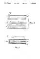
- FIG. 2is a cross-sectional view of a multilayer device made according to a second embodiment of the present invention.
- FIG. 3is a cross-section view showing the individual layers that comprise the multilayer PCB of FIG. 2.
- a first embodiment of the present inventionis a process 10 for making a multi-layer printed circuit board (PCB) that comprises a rheologic bonding (under temperature and pressure), in a step 12, of a double-treated copper foil (available from Nippon Mining) to a substrate comprising an alloy of epoxy and polyphenylene oxide (PPO) resin (available under the GETEK trademark of General Electric Electromaterials) to make a copper clad laminate.
- a double-treated copper foilis an important part of the present invention for the copper foil ultimately forms inside conductive layers of a multilayer package.
- Single-treated copper foilmay be used for conductive layers that wind up on the outsides of the multilayer package.
- a preclean sub-process 14comprises baking the laminate, in a step 16, in an air-circulating oven for four hours at 325° F., dipping, in a step 18, the laminate in a preplating cleaner (e.g., a degreaser), in a step 20 rinsing the laminate in water, in a step 22, dipping the laminate in a microetch (e.g., a 5% solution), in a step 24, rinsing again in water, in a step 26 dipping the laminate in a copper conditioning bath (e.g., an antioxident), in a step 28, rinsing again in water, and in a step 30 drying in an air dryer.
- a preplating cleanere.g., a degreaser
- a microetche.g., a 5% solution
- a fully aqueous dry filmis laminated onto the copper surfaces.
- the dry film laminateis exposed to ultra-violet light, using circuit wiring film patterns.
- the laminatesare then photo-developed.
- a caustic stripperis used to wash away non-exposed areas.
- an alkaline etchantis used to remove the copper not protected by the remaining developed dry film. This is followed by a step 42 that strips off the remaining developed dry film. Copper traces now appear that mimic the film patterns.
- the prior artuses an oxide subprocess 44 that comprises a step 46 in which the laminate is dipped in a preplating cleaner (e.g., a degreaser), a step 48 that rinses the laminate in water, a step 50 of dipping the laminate in a microetch (e.g., a 5% solution), a step 52 that rinses the laminate in water, a step 54 that rinses the laminate in de-ionized water, a step 56 that dips the laminate in a caustic soda solution (e.g., 10% solution), a step 58 that dips the laminate in a brown oxide, and a step 60 that dips the laminate in de-ionized water.
- a preplating cleanere.g., a degreaser
- a step 48that rinses the laminate in water
- a microetche.g., a 5% solution
- a step 52that rinses the laminate in water
- a step 54that rinses the laminate in de-ionized water
- the first embodiment of the present inventiondoes not include oxide subprocess 44, but rather proceeds directly from step 42 to a step 62 in which an air-circulating oven is used for thirty minutes at 260° F. to dry off excess moisture left over from the wet processes.
- Multilayer boardsare then made in a step 64 by laying-up individual panels with copper clad on the outside of the stack.
- the layered boardsare then laminated under pressure and heat, 200° C. for ninety minutes at 125 PSI, with a vacuum assist, or 200 PSI without.
- the flashingis then sheared off.
- holesare drilled for "vias" (connections between circuit layers) and component mounting, which may be accomplished by using FR-4 parameters.
- a step 72resin smear inside the drilled holes is removed, thus exposing copper interconnects in the circuit layers.
- copperis electro-deposited inside the drill holes, thus completing the electrical connections between layers.
- a step 76the outermost copper layers are laminated with a fully aqueous dry film.
- the dry film laminateis exposed to ultra-violet light using additional film patterns.
- a step 80the outside layers are then photo-developed.
- a caustic stripperis used to wash away non-exposed areas.
- an alkaline etchantis used to remove the copper not protected by the remaining developed dry film.
- a step 86that strips off the remaining developed dry film. Copper traces (conductors) appear that mimic the additional proprietary film patterns.
- an air-circulating ovenis used for thirty minutes at 260° F. to dry off excess moisture left over from the wet processes.
- a photo-imagable solder maskis screened on and heat cured in an air-circulating oven.
- a thin coating of 63% solder to 37% nickelis hot bathed into the exposed copper in the vias and elsewhere not protected by the solder mask.
- a step 94a continuity check of the board is done before routing each individual board from a frame of several.
- a step 96a final inspection completes the process.
- the copper foil used in step 12preferably has no layer of copper that has oxidized. It is conventional, prior art practice to grow a layer of oxide of copper on the copper foil to promote the adhesion (rheologic bonding) of the copper foil to the substrate. But at frequencies over one gigahertz, such an oxide layer interferes with high frequency currents that tend to flow on the outside surfaces of conductors due to a phenomenon known as the "skin effect". The complete elimination of the oxide layer is frequently not economically practical. However, available techniques can be employed (e.g., nitrogen atmospheres) to completely eliminate the growth of an oxide layer on the copper foil should the expense be justifiable. The elimination of the prior art steps of deliberately introducing oxide will produce some benefits. Using preclean subprocess 14 and eliminating oxide subprocess 44 reduces oxide layer thickness on the respective copper foil surfaces to under one thousand Angstroms (1000 ⁇ ).
- Press Cycle Athe press temperature is 350° F.
- the starting low pressureis 25 PSI until the panel (laminate) temperature reaches 260° F.
- a high pressure of 200 PSI125 PSI with vacuum assist
- the heat rise rateshould be 10°-15° F. per minute.
- the cool downshould be less than 10° F. per minute.
- a post bake of 390° F. with a minimum of 75 minutes at a material temperature of 375° F.should follow.
- Press Cycle Bthe press temperature is 375° F.
- the starting low pressureis 25 PSI until the panel (laminate) temperature reaches 260° F.
- a high pressure of 200 PSI125 PSI with vacuum assist
- the heat rise rateshould be 10°-15° F. per minute from 175° F. to 275° F.
- the cool downshould be less than 10° F. per minute.
- a post bakeis not required.
- a second embodiment of the present inventionis a microwave device 100 that comprises a printed circuit board (PCB) 102 made by the above process 10.
- a module 103 operating at microwave frequenciesuses a pair of outside conductors 104 and 106, and a pair of inside conductors 108 and 110 to carry signals in excess of one gigahertz.
- the PPO material in PCB 102exhibits stable dielectric constants (DK) between one and twenty gigahertz, and has been tested to be about 3.2 with a dissipation factor of 0.01 to 0.015.
- PCB 102is shown to be comprised of a single-sided, single-treated copper clad laminate 112, a double sided, double-treated copper clad laminate 114, and oxided foil 106.
- a pair of plies of prepreg 116 and 118e.g., General Electric TO(B) prepreg 106 glass
- a pair of plies of prepreg 120 and 122e.g., General Electric TO(B) prepreg 106 glass
- a ply 124 of preprege.g., General Electric T3(B) prepreg 2313 glass
Landscapes
- Engineering & Computer Science (AREA)
- Microelectronics & Electronic Packaging (AREA)
- Manufacturing & Machinery (AREA)
- Production Of Multi-Layered Print Wiring Board (AREA)
Abstract
Description
Claims (4)
Priority Applications (1)
| Application Number | Priority Date | Filing Date | Title |
|---|---|---|---|
| US07/830,733US5268064A (en) | 1992-02-04 | 1992-02-04 | Copper clad epoxy printed circuit board suitable for microwave frequencies encountered in GPS receivers |
Applications Claiming Priority (1)
| Application Number | Priority Date | Filing Date | Title |
|---|---|---|---|
| US07/830,733US5268064A (en) | 1992-02-04 | 1992-02-04 | Copper clad epoxy printed circuit board suitable for microwave frequencies encountered in GPS receivers |
Publications (1)
| Publication Number | Publication Date |
|---|---|
| US5268064Atrue US5268064A (en) | 1993-12-07 |
Family
ID=25257592
Family Applications (1)
| Application Number | Title | Priority Date | Filing Date |
|---|---|---|---|
| US07/830,733Expired - Fee RelatedUS5268064A (en) | 1992-02-04 | 1992-02-04 | Copper clad epoxy printed circuit board suitable for microwave frequencies encountered in GPS receivers |
Country Status (1)
| Country | Link |
|---|---|
| US (1) | US5268064A (en) |
Cited By (29)
| Publication number | Priority date | Publication date | Assignee | Title |
|---|---|---|---|---|
| US5897605A (en)* | 1996-03-15 | 1999-04-27 | Sirf Technology, Inc. | Spread spectrum receiver with fast signal reacquisition |
| US5901171A (en)* | 1996-03-15 | 1999-05-04 | Sirf Technology, Inc. | Triple multiplexing spread spectrum receiver |
| WO1999045752A1 (en)* | 1998-03-05 | 1999-09-10 | Obducat Ab | Electric conductor with a surface structure in the form of flanges and etched grooves |
| US5959256A (en)* | 1995-01-23 | 1999-09-28 | Mitsui Mining & Smelting Co., Ltd. | Multilayer printed wiring board |
| US6018704A (en)* | 1996-04-25 | 2000-01-25 | Sirf Tech Inc | GPS receiver |
| US6041280A (en)* | 1996-03-15 | 2000-03-21 | Sirf Technology, Inc. | GPS car navigation system |
| US6047017A (en)* | 1996-04-25 | 2000-04-04 | Cahn; Charles R. | Spread spectrum receiver with multi-path cancellation |
| WO2000021344A1 (en)* | 1998-10-06 | 2000-04-13 | Telefonaktiebolaget Lm Ericsson (Publ) | Printed board assembly and method of its manufacture |
| US6125325A (en)* | 1996-04-25 | 2000-09-26 | Sirf Technology, Inc. | GPS receiver with cross-track hold |
| US6197898B1 (en) | 1997-11-18 | 2001-03-06 | General Electric Company | Melt-mixing thermoplastic and epoxy resin above Tg or Tm of thermoplastic with curing agent |
| US6198765B1 (en) | 1996-04-25 | 2001-03-06 | Sirf Technologies, Inc. | Spread spectrum receiver with multi-path correction |
| US6249542B1 (en) | 1997-03-28 | 2001-06-19 | Sirf Technology, Inc. | Multipath processing for GPS receivers |
| US6282231B1 (en) | 1999-12-14 | 2001-08-28 | Sirf Technology, Inc. | Strong signal cancellation to enhance processing of weak spread spectrum signal |
| US6366250B1 (en) | 1999-12-09 | 2002-04-02 | Sirf Technology, Inc. | Wrist mounted wireless instrument and antenna apparatus |
| US6393046B1 (en) | 1996-04-25 | 2002-05-21 | Sirf Technology, Inc. | Spread spectrum receiver with multi-bit correlator |
| US6729023B2 (en)* | 2000-05-26 | 2004-05-04 | Visteon Global Technologies, Inc. | Method for making a multi-layer circuit board assembly having air bridges supported by polymeric material |
| WO2004054332A3 (en)* | 2002-12-06 | 2004-11-18 | Igor Anatolievich Abrosimov | Strip-line topology for a high speed pcb with low dissipation |
| US6917644B2 (en) | 1996-04-25 | 2005-07-12 | Sirf Technology, Inc. | Spread spectrum receiver with multi-path correction |
| US20090232972A1 (en)* | 2004-07-08 | 2009-09-17 | Jurgen Schulz-Harder | Method for the production of a metal-ceramic substrate |
| EP2253669A1 (en)* | 2009-05-20 | 2010-11-24 | Valtion Teknillinen Tutkimuskeskus | PPO composition as bonding base for electronic components, and method |
| US20120030942A1 (en)* | 2010-08-09 | 2012-02-09 | Samsung Electro-Mechanics Co., Ltd. | Method for manufacturing multi-layer printed circuit board |
| US20120241810A1 (en)* | 2010-11-30 | 2012-09-27 | Zheng Wang | Printing circuit board with micro-radiators |
| US20130015234A1 (en)* | 2010-06-11 | 2013-01-17 | Global Unichip Corp. | Method of Forming a Package Substrate |
| US20130019470A1 (en)* | 2011-07-22 | 2013-01-24 | Ict-Lanto Limited | Method of manufacturing three-dimensional circuit |
| US20130120949A1 (en)* | 2011-11-16 | 2013-05-16 | Tien-Wei SUN | Method of manufacturing passive component module |
| US20130232784A1 (en)* | 2012-03-06 | 2013-09-12 | Ngk Spark Plug Co., Ltd | Method of manufacturing wiring substrate |
| US20130269183A1 (en)* | 2012-03-28 | 2013-10-17 | Ttm Technologies, Inc. | Printed circuit board interconnect assembly and method |
| US9247649B2 (en) | 2013-05-06 | 2016-01-26 | Globalfoundries Inc. | Printed circuit boards fabricated using congruent molds |
| US20230301347A1 (en)* | 2020-09-09 | 2023-09-28 | Jt International Sa | Electronic Smoking Device Comprising a Rigidised Flexible PCB |
Citations (4)
| Publication number | Priority date | Publication date | Assignee | Title |
|---|---|---|---|---|
| US3177103A (en)* | 1961-09-18 | 1965-04-06 | Sauders Associates Inc | Two pass etching for fabricating printed circuitry |
| US4659425A (en)* | 1986-02-03 | 1987-04-21 | Ibm Corporation | Continuous process for the manufacture of printed circuit boards |
| US4902556A (en)* | 1989-01-27 | 1990-02-20 | The B. F. Goodrich Company | Multi-layer polynorbornene and epoxy laminates and process for making the same |
| US4917758A (en)* | 1988-05-20 | 1990-04-17 | Mitsubishi Gas Chemical Company, Inc. | Method for preparing thin copper foil-clad substrate for circuit boards |
- 1992
- 1992-02-04USUS07/830,733patent/US5268064A/ennot_activeExpired - Fee Related
Patent Citations (4)
| Publication number | Priority date | Publication date | Assignee | Title |
|---|---|---|---|---|
| US3177103A (en)* | 1961-09-18 | 1965-04-06 | Sauders Associates Inc | Two pass etching for fabricating printed circuitry |
| US4659425A (en)* | 1986-02-03 | 1987-04-21 | Ibm Corporation | Continuous process for the manufacture of printed circuit boards |
| US4917758A (en)* | 1988-05-20 | 1990-04-17 | Mitsubishi Gas Chemical Company, Inc. | Method for preparing thin copper foil-clad substrate for circuit boards |
| US4902556A (en)* | 1989-01-27 | 1990-02-20 | The B. F. Goodrich Company | Multi-layer polynorbornene and epoxy laminates and process for making the same |
Cited By (50)
| Publication number | Priority date | Publication date | Assignee | Title |
|---|---|---|---|---|
| US5959256A (en)* | 1995-01-23 | 1999-09-28 | Mitsui Mining & Smelting Co., Ltd. | Multilayer printed wiring board |
| US6788735B2 (en) | 1996-03-15 | 2004-09-07 | Sirf Technology, Inc. | Triple multiplexing spread spectrum receiver |
| US5901171A (en)* | 1996-03-15 | 1999-05-04 | Sirf Technology, Inc. | Triple multiplexing spread spectrum receiver |
| US7295633B2 (en) | 1996-03-15 | 2007-11-13 | Sirf Technology, Inc. | Triple multiplexing spread spectrum receiver |
| US6522682B1 (en) | 1996-03-15 | 2003-02-18 | Sirf Technology, Inc. | Triple multiplexing spread spectrum receiver |
| US6041280A (en)* | 1996-03-15 | 2000-03-21 | Sirf Technology, Inc. | GPS car navigation system |
| US6292749B2 (en) | 1996-03-15 | 2001-09-18 | Sirf Technology, Inc. | GPS receiver with cross-track hold |
| US5897605A (en)* | 1996-03-15 | 1999-04-27 | Sirf Technology, Inc. | Spread spectrum receiver with fast signal reacquisition |
| US6018704A (en)* | 1996-04-25 | 2000-01-25 | Sirf Tech Inc | GPS receiver |
| US6125325A (en)* | 1996-04-25 | 2000-09-26 | Sirf Technology, Inc. | GPS receiver with cross-track hold |
| US6198765B1 (en) | 1996-04-25 | 2001-03-06 | Sirf Technologies, Inc. | Spread spectrum receiver with multi-path correction |
| US6236937B1 (en) | 1996-04-25 | 2001-05-22 | Sirf Technology, Inc. | GPS receiver with cross-track hold |
| US6917644B2 (en) | 1996-04-25 | 2005-07-12 | Sirf Technology, Inc. | Spread spectrum receiver with multi-path correction |
| US6633814B2 (en) | 1996-04-25 | 2003-10-14 | Sirf Technology, Inc. | GPS system for navigating a vehicle |
| US6047017A (en)* | 1996-04-25 | 2000-04-04 | Cahn; Charles R. | Spread spectrum receiver with multi-path cancellation |
| US6574558B2 (en) | 1996-04-25 | 2003-06-03 | Sirf Technology, Inc. | GPS receiver with cross-track hold |
| US6393046B1 (en) | 1996-04-25 | 2002-05-21 | Sirf Technology, Inc. | Spread spectrum receiver with multi-bit correlator |
| US6400753B1 (en) | 1996-04-25 | 2002-06-04 | Sirf Technology, Inc. | Pseudo-noise correlator for a GPS spread spectrum receiver |
| US6421609B2 (en) | 1996-04-25 | 2002-07-16 | Sirf Technology, Inc. | GPS receiver with cross-track hold |
| US6249542B1 (en) | 1997-03-28 | 2001-06-19 | Sirf Technology, Inc. | Multipath processing for GPS receivers |
| US6760364B2 (en) | 1997-03-28 | 2004-07-06 | Sirf Technology, Inc. | Multipath processing for GPS receivers |
| US6466612B2 (en) | 1997-03-28 | 2002-10-15 | Sirf Technology, Inc. | Multipath processing for GPS receivers |
| US7301992B2 (en) | 1997-03-28 | 2007-11-27 | Sirf Technology, Inc. | Multipath processing for GPS receivers |
| US6197898B1 (en) | 1997-11-18 | 2001-03-06 | General Electric Company | Melt-mixing thermoplastic and epoxy resin above Tg or Tm of thermoplastic with curing agent |
| US6407340B1 (en) | 1998-03-05 | 2002-06-18 | Obducat Ab | Electric conductor with a surface structure in the form of flanges and etched grooves |
| WO1999045752A1 (en)* | 1998-03-05 | 1999-09-10 | Obducat Ab | Electric conductor with a surface structure in the form of flanges and etched grooves |
| WO2000021344A1 (en)* | 1998-10-06 | 2000-04-13 | Telefonaktiebolaget Lm Ericsson (Publ) | Printed board assembly and method of its manufacture |
| US6552265B1 (en) | 1998-10-06 | 2003-04-22 | Telefonaktiebolaget Lm Ericsson | Printed board assembly and method of its manufacture |
| US6366250B1 (en) | 1999-12-09 | 2002-04-02 | Sirf Technology, Inc. | Wrist mounted wireless instrument and antenna apparatus |
| US7116704B2 (en) | 1999-12-14 | 2006-10-03 | Sirf Technology, Inc. | Strong signal cancellation to enhance processing of weak spread spectrum signal |
| US6282231B1 (en) | 1999-12-14 | 2001-08-28 | Sirf Technology, Inc. | Strong signal cancellation to enhance processing of weak spread spectrum signal |
| US6729023B2 (en)* | 2000-05-26 | 2004-05-04 | Visteon Global Technologies, Inc. | Method for making a multi-layer circuit board assembly having air bridges supported by polymeric material |
| WO2004054332A3 (en)* | 2002-12-06 | 2004-11-18 | Igor Anatolievich Abrosimov | Strip-line topology for a high speed pcb with low dissipation |
| US8683682B2 (en)* | 2004-07-08 | 2014-04-01 | Curamik Electronics Gmbh | Method for the production of a metal-ceramic substrate |
| US20090232972A1 (en)* | 2004-07-08 | 2009-09-17 | Jurgen Schulz-Harder | Method for the production of a metal-ceramic substrate |
| EP2253669A1 (en)* | 2009-05-20 | 2010-11-24 | Valtion Teknillinen Tutkimuskeskus | PPO composition as bonding base for electronic components, and method |
| US9464190B2 (en) | 2009-05-20 | 2016-10-11 | Teknologian Tutkimuskeskus Vtt | Bonding base for electronic components, and method |
| US20130015234A1 (en)* | 2010-06-11 | 2013-01-17 | Global Unichip Corp. | Method of Forming a Package Substrate |
| US9449909B2 (en)* | 2010-06-11 | 2016-09-20 | Taiwan Semiconductor Manufacturing Company, Ltd. | Method of forming a package substrate |
| US9060458B2 (en)* | 2010-08-09 | 2015-06-16 | Samsung Electro-Mechanics Co., Ltd. | Method for manufacturing multi-layer printed circuit board |
| US20120030942A1 (en)* | 2010-08-09 | 2012-02-09 | Samsung Electro-Mechanics Co., Ltd. | Method for manufacturing multi-layer printed circuit board |
| US20120241810A1 (en)* | 2010-11-30 | 2012-09-27 | Zheng Wang | Printing circuit board with micro-radiators |
| US20130019470A1 (en)* | 2011-07-22 | 2013-01-24 | Ict-Lanto Limited | Method of manufacturing three-dimensional circuit |
| US20130120949A1 (en)* | 2011-11-16 | 2013-05-16 | Tien-Wei SUN | Method of manufacturing passive component module |
| US9125320B2 (en)* | 2011-11-16 | 2015-09-01 | Dyi-chung Hu | Method of manufacturing passive component module |
| US20130232784A1 (en)* | 2012-03-06 | 2013-09-12 | Ngk Spark Plug Co., Ltd | Method of manufacturing wiring substrate |
| US20130269183A1 (en)* | 2012-03-28 | 2013-10-17 | Ttm Technologies, Inc. | Printed circuit board interconnect assembly and method |
| US9532465B2 (en)* | 2012-03-28 | 2016-12-27 | Ttm Technologies, Inc. | Method of fabricating a printed circuit board interconnect assembly |
| US9247649B2 (en) | 2013-05-06 | 2016-01-26 | Globalfoundries Inc. | Printed circuit boards fabricated using congruent molds |
| US20230301347A1 (en)* | 2020-09-09 | 2023-09-28 | Jt International Sa | Electronic Smoking Device Comprising a Rigidised Flexible PCB |
Similar Documents
| Publication | Publication Date | Title |
|---|---|---|
| US5268064A (en) | Copper clad epoxy printed circuit board suitable for microwave frequencies encountered in GPS receivers | |
| US7351915B2 (en) | Printed circuit board including embedded capacitor having high dielectric constant and method of fabricating same | |
| US4915983A (en) | Multilayer circuit board fabrication process | |
| US7092237B2 (en) | Printed circuit board with embedded capacitors therein, and process for manufacturing the same | |
| JP4288266B2 (en) | Manufacturing method of printed circuit board with built-in multilayer capacitor | |
| US4388136A (en) | Method of making a polyimide/glass hybrid printed circuit board | |
| JP2004522304A (en) | Method of forming a printed circuit board and printed circuit board formed by this method | |
| JPS61220499A (en) | Hybrid multilayer wiring board | |
| KR100867442B1 (en) | Improving adhesion strength between conductive paste and lands of printed wiring board, and manufacturing method thereof | |
| US7238891B2 (en) | Circuit board with at least one rigid and at least one flexible area and process for producing rigid-flexible circuit boards | |
| JP4129166B2 (en) | Electrolytic copper foil, film with electrolytic copper foil, multilayer wiring board, and manufacturing method thereof | |
| US6651324B1 (en) | Process for manufacture of printed circuit boards with thick copper power circuitry and thin copper signal circuitry on the same layer | |
| US5679498A (en) | Method for producing high density multi-layer integrated circuit carriers | |
| US5779836A (en) | Method for making a printed wiring board | |
| KR100674321B1 (en) | Printed circuit board with improved heat dissipation and its manufacturing method | |
| WO1988004877A1 (en) | Multilayer circuit board fabrication process | |
| US6586687B2 (en) | Printed wiring board with high density inner layer structure | |
| JPH0722725A (en) | Circuit board with thin-film capacitor and its manufacture | |
| RU2010462C1 (en) | Multilayer printed circuit board with components | |
| US5114518A (en) | Method of making multilayer circuit boards having conformal Insulating layers | |
| JP2002124415A (en) | Printed circuit board for high frequency and its manufacturing method | |
| CN87100490A (en) | method for manufacturing multilayer printed circuit board | |
| JP2003046247A (en) | Multilayer printed wiring board and its manufacturing method | |
| JPH1174641A (en) | Multilayer wiring board | |
| EP0264617A1 (en) | Multilayer circuit board and method of manufacture therefor |
Legal Events
| Date | Code | Title | Description |
|---|---|---|---|
| AS | Assignment | Owner name:TRIMBLE NAVIGATION LIMITED, CALIFORNIA Free format text:ASSIGNMENT OF ASSIGNORS INTEREST.;ASSIGNORS:WOO, ARTHUR N.;TOM, PAUL K.;REEL/FRAME:006019/0670 Effective date:19920204 | |
| FEPP | Fee payment procedure | Free format text:PAYOR NUMBER ASSIGNED (ORIGINAL EVENT CODE: ASPN); ENTITY STATUS OF PATENT OWNER: LARGE ENTITY | |
| FPAY | Fee payment | Year of fee payment:4 | |
| AS | Assignment | Owner name:ABN AMRO BANK N.V., AS AGENT, ILLINOIS Free format text:SECURITY AGREEMENT;ASSIGNOR:TRIMBLE NAVIGATION LIMITED;REEL/FRAME:010996/0643 Effective date:20000714 | |
| FPAY | Fee payment | Year of fee payment:8 | |
| REMI | Maintenance fee reminder mailed | ||
| LAPS | Lapse for failure to pay maintenance fees | ||
| LAPS | Lapse for failure to pay maintenance fees | Free format text:PATENT EXPIRED FOR FAILURE TO PAY MAINTENANCE FEES (ORIGINAL EVENT CODE: EXP.); ENTITY STATUS OF PATENT OWNER: LARGE ENTITY | |
| STCH | Information on status: patent discontinuation | Free format text:PATENT EXPIRED DUE TO NONPAYMENT OF MAINTENANCE FEES UNDER 37 CFR 1.362 | |
| FP | Lapsed due to failure to pay maintenance fee | Effective date:20051207 |