US5263191A - Method and circuit for processing and filtering signals - Google Patents
Method and circuit for processing and filtering signalsDownload PDFInfo
- Publication number
- US5263191A US5263191AUS07/806,058US80605891AUS5263191AUS 5263191 AUS5263191 AUS 5263191AUS 80605891 AUS80605891 AUS 80605891AUS 5263191 AUS5263191 AUS 5263191A
- Authority
- US
- United States
- Prior art keywords
- signal
- digital data
- digital
- data signals
- produce
- Prior art date
- Legal status (The legal status is an assumption and is not a legal conclusion. Google has not performed a legal analysis and makes no representation as to the accuracy of the status listed.)
- Expired - Lifetime
Links
Images


Classifications
- H—ELECTRICITY
- H03—ELECTRONIC CIRCUITRY
- H03H—IMPEDANCE NETWORKS, e.g. RESONANT CIRCUITS; RESONATORS
- H03H17/00—Networks using digital techniques
- H03H17/02—Frequency selective networks
- H03H17/0248—Filters characterised by a particular frequency response or filtering method
- H03H17/0251—Comb filters
Definitions
- This inventionrelates to methods and circuits for processing and filtering signals. Such methods and circuits can be particularly adapted to reduce amplitude variations in angle modulated radio frequency signals, or to provide comb notch filtering that removes interference of a repetitive nature.
- Multipath phenomenaresults from multiple paths taken by a transmitted radio frequency signal before the signal reaches a receiver. Transmission of the signal along these paths results in constructive and destructive interference which causes amplitude variations that are a function of the signal's instantaneous frequency. These variations in amplitude complicate subsequent signal processing. For example, in the reception of radio frequency signals, a situation is frequently encountered in which a weak signal of interest (SOI) is subject to interference by a strong interfering signal having a frequency band which encompasses that of the SOI.
- the interfering signalmay be, for example, a jamming signal or a commercial radio or television signal. If the interfering signal is an angle modulated signal, variations in amplitude whether caused by multipath phenomena or otherwise, can further mask the signal of interest, making detection of the signal of interest more difficult.
- Interference of a repetitive naturecan also cause harmonic interference, in which case it is desirable to remove the harmonic components of a signal.
- a comb notch filtermay be used for such purposes.
- the present inventionseeks to provide a method and circuit for processing radio frequency signals to filter the signals or to remove the effects of amplitude variations wherein the amplitude variations are correlated with the instantaneous frequency of the signal.
- a circuit for processing electrical signals 10 constructed in accordance with this inventionincludes: a memory having a plurality of addresses for storing a plurality of first digital data signals, each representative of an instantaneous amplitude of a first input signal; means for selecting one of the first digital data signals in response to a second input signal; means for combining the selected one of the first digital data signals with a second digital data signal representative of a subsequent instantaneous amplitude of the first input signal, to produce a digital difference signal; means for producing a first output signal in response to the digital difference signal; and means for combining the digital difference signal and the selected one of the first digital data signals to produce a modified digital data signal and for replacing the selected first digital data signal with the modified digital data signal in the memory.
- the above circuitcan serve as a part of a circuit for removing the effects of amplitude variations in a radio frequency signal, constructed in accordance with this invention which comprises: a memory having a plurality of addresses for storing a plurality of first digital data signals, each representative of an instantaneous amplitude of a first input signal, wherein the amplitude variations are correlated with the instantaneous frequency of the signal; a first analog to digital converter for producing an address signal for selecting one of the first digital data signals in response to a first input signal, the first input signal being correlated with the interfering signal; a first adder for combining the selected one of the first digital data signals with a second digital data signal representative of a subsequent instantaneous amplitude of the composite signal, to produce a digital difference signal; a first digital to analog converter for producing a first analog output signal in response to the digital difference signal; and a second adder for combining the digital difference signal and the selected one of the first digital data signal to produce a modified digital data signal and for replacing the selected
- the inventionalso includes a method for processing electrical signals comprising the steps of: providing a memory having a plurality of addresses for storing a plurality of first digital data signals, each representative of an instantaneous amplitude of a first input signal; selecting one of the first digital data signals in response to a second input signal; combining the selected one of the first digital data signals with a second digital data signal representative of a subsequent instantaneous amplitude of the first input signal, to produce a digital difference signal; producing a first output signal in response to the digital difference signal; and combining the digital difference signal and the selected first digital data signal to produce a modified digital data signal and for replacing the selected one of the first digital data signals with the modified digital data signal in the memory.
- the inventionfurther encompasses the method for compensating for amplitude variations in an angle modulated radio frequency signal, performed by the above circuit, comprising the steps of: providing a memory having a plurality of addresses for storing a plurality of first digital data signals, each representative of an instantaneous amplitude of a composite signal, wherein the composite signal includes a signal of interest and an interfering signal; selecting one of the first digital data signals in response to a first input signal, the first input signal being correlated with the interfering signal; combining the selected one of the first digital data signals with a second digital data signal representative of a subsequent instantaneous amplitude of the composite signal, to produce a digital difference signal; producing a first analog output signal in response to the digital difference signal; combining the digital difference signal and the selected one of the first digital data signals to produce a modified digital data signal; and replacing the selected first digital data signal with the modified digital data signal in the memory.
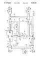
- FIG. 1is a block diagram of an interference suppression circuit which includes an equalization circuit constructed in accordance with this invention.
- FIG. 2is a block diagram of the equalization circuit of FIG. 1;
- FIG. 3is a block diagram of a filter circuit constructed in accordance with this invention.
- FIGS. 4 and 5are diagrams which illustrate the operation of the filter of FIG. 3.
- FIG. 1is a block diagram of an interference suppression circuit 10, having an equalization circuit 12 constructed in accordance with this invention.
- the circuit of FIG. 1provides non-cooperative suppression of high-level interference signals to enhance the detection of a co-channel low-level signal of interest (SOI).
- non-cooperative suppressionrefers to suppression of an interfering signal which does not require a reference sample of the interfering signal.
- the circuitoperates on an interference corrupted signal to produce an enhanced version of the desired SOI.
- the circuit of FIG. 1can be readily retrofitted within the intermediate frequency (IF) stage of existing receiver systems.
- IFintermediate frequency
- a composite signalincluding both an angle modulated interfering signal (I) and a signal of interest (SOI) is supplied to the interference suppression circuit 10 by way of input line 14.
- a signal splitter 16splits the composite signal and delivers it to a first channel 18 and a second channel 20.
- An error signal on line 22is amplified by amplifier 24 and used by a voltage controlled oscillator 26 to produce a reference signal on line 28.
- the reference signal on line 28is split by a splitter 30 and sent to first and second in-phase/quadrature splitters 32 and 34, respectively.
- the in-phase/quadrature splittersproduce a first output which is the in phase component of the reference signal (0 degrees) and a second output which is the quadrature component of the reference signal (90 degrees).
- a first mixer 36mixes the composite signal on line 38 with the in phase component of the reference signal on line 40 to produce a first compound signal on line 42.
- a filter 44removes selected components of the first compound signal to produce a first filtered signal on line 46.
- the filtered signalis delivered via resistor 48 to line 50 where it is combined with a second filtered signal from filter 72 and passed to equalization circuit 12.
- the equalization circuitproduces a modified signal on line 52 which is delivered via resistor 54 to a second mixer 56.
- the second mixermixes the modified signal on line 54 with an in phase component of the reference signal on line 58 to produce a second compound signal on line 60.
- a third mixer 62mixes the composite signal on line 64 with a quadrature component of the reference signal on line 66 to produce a third compound signal on line 68.
- the error signal on line 22is the difference in voltage of the first and third compound signals as produced at the output of summation point 70.
- a second filter 72which is matched to filter 44, removes selected components of the third compound signal and produces the second filtered signal on line 74.
- the second filtered signalis combined with the first filtered signal and delivered to the equalization circuit 12 via resistor 76 and line 50.
- a fourth mixer 78receives the modified signal on line 52, via resistor 80 and mixes the modified signal with a quadrature component of the reference signal on line 82 to produce a fourth compound signal on line 84.
- the second and fourth compound signalsare combined by combiner 86 to produce an output signal on line 88.
- the spectral power density of the signal of interest in the output signalis greater than the spectral power density of the interfering signal in the output signal. Therefore the signal of interest in the output signal can be easily captured by well known signal capture circuits.
- the amplified error signal on line 90is correlated with the interfering signal portion of the first and second filtered signals. This correlated signal is used to select addresses in a memory of the equalizer as is discussed below.
- the circuit of FIG. 1is particularly directed to those instances where the angle modulated interfering signal (I) has a constant envelope with a bandwidth encompassing that of the signal of interest (SOI).
- the interfering signalmay have an inherent amplitude variation which is dependent upon the amount of angle modulation, and will have additional amplitude variation due to multipath phenomena. This amplitude variation is relatively well defined.
- the circuit of FIG. 1is provided as an example of the type of circuit which can benefit from the addition of the equalization circuit of this invention. A detailed description of the operation of the circuit of FIG. 1 is not required in order to practice the present invention, since the invention can be applied to a wide variety of circuits in which an angle modulated signal is subject to undesired amplitude variations.
- FIG. 2is a block diagram of an equalization circuit constructed in accordance with this invention, and suitable for use as the equalization circuit in FIG. 1.
- Circuits constructed in accordance with the equalization circuit of FIG. 2estimate the amplitude variation signature in the interfering signal and subtract it from the filtered signals to reduce the amount of amplitude variation in the resulting modified filtered signal. The estimation is accomplished by repeatedly sampling the input signal and combining the sampled value with a previously stored value to obtain an updated value which replaces the previously stored value. The updated value is typically closer to the previously stored value than the sampled value.
- a first analog to digital converter 92receives the error signal (ES) on line 90.
- the error signalis correlated with an interfering signal wherein the interfering signal is one component of a composite signal on line 50.
- the composite signal on line 50also includes a signal of interest.
- Analog to digital converter 92produces a digital output signal, representative of the instantaneous amplitude of the signal on line 90, on data bus 94.
- the data signal on line 94is used to select an address in memory 96.
- memory 96includes a plurality of addresses for storing first digital data signals which are representative of the previous values of the composite signal.
- a second analog to digital converter 98receives the composite signal, including both the interfering signal (I) and the signal of interest (SOI) on line 50, and produces a digital output signal on line 100 that is representative of the instantaneous value of the composite signal.
- Clock 102controls the sequence of operations performed by the circuit of FIG. 2.
- analog to digital converters 92 and 98produce their respective output signals.
- the analog to digital convertersalso produce data ready signals on lines 104 and 106. These data ready signals are received by AND gate 108 and used to produce a voltage pulse on line 110.
- the voltage pulse on line 110passes to delay circuit 112, which may be a shift register.
- Delay circuit 112then produces output pulses on lines 114, 116 and 118.
- the first data signalis selected by the address identified by the signal on bus 94, and read out onto bus 120. Alternatively, selection of the first data signal may be done utilizing a software loop.
- the selected signalis then frozen by latch 122, which is controlled by a pulse on line 116.
- the frozen signal on bus 124is delivered to adder 126 where it is subtracted from the signal on bus 100 to produce a digital difference signal on bus 128.
- Latch 130freezes the digital difference signal on bus 132 in response to a voltage pulse on line 118.
- a first digital to analog converter 134converts the digital signal on bus 132 to an analog output signal (AOS) on line 52. When this circuit is used in the circuit of FIG. 1, the output signal from digital to analog converter 134 is the modified filtered signal.
- AOSanalog output signal
- Scaling circuit 136divides the digital difference signal on bus 128 by a preselected number to produce an incremental adjustment signal on bus 138.
- the incremental adjustment signal on bus 138is then added to the first digital data signal on bus 124 by adder 140 to obtain a modified digital data signal on bus 142.
- a pulse on line 114enables memory 96 to replace the selected first digital data signal previously read from the memory with the digital data signal on bus 142 at the address identified by the signal on bus 94.
- a second digital to analog converter 144converts the first digital signal on bus 124 into a second output signal (SOS) on line 146.
- the second output signal(which is not used by the circuit of FIG. 1 ) is representative of the interfering signal component of the composite signal.
- the circuit of FIG. 2uses a successive estimation technique to update the data in the memory so that the stored data approaches an accurate representation of the amplitude variation of the interfering signal.
- the amount by which the values of the stored data are adjusted (attack rate)is controlled by changing the value of the divisor in scaling circuit 136.
- the input signal on line 50is a composite signal which includes a signal of interest and an undesired interfering signal, wherein the signal of interest can be considered to be a deviation from the average of the composite signal.
- the input signal on line 90is a signal which is correlated with the interfering signal.
- the output signal on line 52is an uncorrelated amplitude modulated signal which is representative of the signal of interest.
- the output signal on line 146is a correlated amplitude modulated signal representative of the interfering signal.
- this inventioncan enhance the interception of low-level signals of interest in the presence of strong interference by reducing the interference due to amplitude variations in the interfering signal which tend to mask the signal of interest.
- the inventionis also useful in circuits used to suppress co-site/co-channel interference in tactical and strategic communications systems.
- interfering signal Ypresent on line 50 or bus 100
- Ycan be represented as a polynomial of the form: ##EQU1## where X is the interfering signal or value on line 90 or bus 94.
- the circuits of this inventionlearn the coefficients C n of the terms of the polynomial and subtract those terms from the composite signal, within the limits of the digital quantization. This is accomplished by using a memory having individual bins for each level of the interfering signal, thereby permitting each level to be handled separately.
- FIG. 3is a block diagram of a comb notch filter which uses the circuit of this invention.
- This circuitis similar to the circuit of FIG. 2 except that the analog to digital converter 91 in FIG. 2 has been replaced by a counter 144.
- the signal to be filteredis applied to input line 50.
- Clock 102controls the sampling rate of analog to digital converter 98 and also increments the counter to provide an address location on bus 94.
- the output on line 52is an uncorrelated notched output and is illustrated in FIG. 4, wherein C is the clock frequency and M is the maximum address on the data bus 94.
- the amplitude in FIG. 4is the ratio of the amplitudes of the signals on line 52 and 50.
- the width of the notch Wis directly proportional to the C/M ratio and inversely proportional to 2 n .
- the output on line 146is a correlated bandpass output and is illustrated in FIG. 5, wherein C is the clock frequency and M is the maximum address on the data bus 94.
- the amplitude in FIG. 5is the ratio of the amplitudes of the signals on lines 146 and 50.
- the width of the bandpass W 1is directly proportional to the C/M ratio and inversely proportional to 2 n .
Landscapes
- Physics & Mathematics (AREA)
- Engineering & Computer Science (AREA)
- Computer Hardware Design (AREA)
- Mathematical Physics (AREA)
- Noise Elimination (AREA)
Abstract
Description
Claims (17)
Priority Applications (2)
| Application Number | Priority Date | Filing Date | Title |
|---|---|---|---|
| US07/806,058US5263191A (en) | 1991-12-11 | 1991-12-11 | Method and circuit for processing and filtering signals |
| US08/134,807US5428834A (en) | 1991-12-11 | 1993-10-12 | Method and circuit for processing and filtering signals |
Applications Claiming Priority (1)
| Application Number | Priority Date | Filing Date | Title |
|---|---|---|---|
| US07/806,058US5263191A (en) | 1991-12-11 | 1991-12-11 | Method and circuit for processing and filtering signals |
Related Child Applications (1)
| Application Number | Title | Priority Date | Filing Date |
|---|---|---|---|
| US08/134,807Continuation-In-PartUS5428834A (en) | 1991-12-11 | 1993-10-12 | Method and circuit for processing and filtering signals |
Publications (1)
| Publication Number | Publication Date |
|---|---|
| US5263191Atrue US5263191A (en) | 1993-11-16 |
Family
ID=25193215
Family Applications (1)
| Application Number | Title | Priority Date | Filing Date |
|---|---|---|---|
| US07/806,058Expired - LifetimeUS5263191A (en) | 1991-12-11 | 1991-12-11 | Method and circuit for processing and filtering signals |
Country Status (1)
| Country | Link |
|---|---|
| US (1) | US5263191A (en) |
Cited By (27)
| Publication number | Priority date | Publication date | Assignee | Title |
|---|---|---|---|---|
| US5428834A (en)* | 1991-12-11 | 1995-06-27 | Xetron Corporation | Method and circuit for processing and filtering signals |
| US5428833A (en)* | 1992-01-22 | 1995-06-27 | Rohde & Schwartz Gmbh & Co., Kg | Arrangement for suppressing spurious signals occurring in the reception signal of a receiver of a high-frequency message transmission system |
| US5519343A (en)* | 1995-07-10 | 1996-05-21 | Fluke Corporation | Two channel direct digital synthesizer with waveform memory interleaving circuit |
| US5875391A (en)* | 1996-07-25 | 1999-02-23 | Unisite, Inc. | Method of and apparatus for performing antenna cosite analysis |
| WO2000027040A3 (en)* | 1998-11-03 | 2000-11-23 | Usa Digital Radio Inc | Method and apparatus for reduction of fm interference for fm in-band on-channel digital audio broadcasting system |
| US6252535B1 (en) | 1997-08-21 | 2001-06-26 | Data Fusion Corporation | Method and apparatus for acquiring wide-band pseudorandom noise encoded waveforms |
| US6430216B1 (en) | 1997-08-22 | 2002-08-06 | Data Fusion Corporation | Rake receiver for spread spectrum signal demodulation |
| US6671340B1 (en) | 2000-06-15 | 2003-12-30 | Ibiquity Digital Corporation | Method and apparatus for reduction of interference in FM in-band on-channel digital audio broadcasting receivers |
| US6771214B2 (en) | 2001-09-12 | 2004-08-03 | Data Fusion Corporation | GPS near-far resistant receiver |
| US7260506B2 (en) | 2001-11-19 | 2007-08-21 | Tensorcomm, Inc. | Orthogonalization and directional filtering |
| US7359465B2 (en) | 2001-09-28 | 2008-04-15 | Tensorcomm, Inc | Serial cancellation receiver design for a coded signal processing engine |
| US7394879B2 (en) | 2001-11-19 | 2008-07-01 | Tensorcomm, Inc. | Systems and methods for parallel signal cancellation |
| US7430253B2 (en) | 2002-10-15 | 2008-09-30 | Tensorcomm, Inc | Method and apparatus for interference suppression with efficient matrix inversion in a DS-CDMA system |
| US7463609B2 (en) | 2005-07-29 | 2008-12-09 | Tensorcomm, Inc | Interference cancellation within wireless transceivers |
| US7477710B2 (en) | 2004-01-23 | 2009-01-13 | Tensorcomm, Inc | Systems and methods for analog to digital conversion with a signal cancellation system of a receiver |
| US20090141775A1 (en)* | 2005-02-25 | 2009-06-04 | Data Fusion Corporation | Mitigating interference in a signal |
| US7577186B2 (en) | 2002-09-20 | 2009-08-18 | Tensorcomm, Inc | Interference matrix construction |
| US7580448B2 (en) | 2002-10-15 | 2009-08-25 | Tensorcomm, Inc | Method and apparatus for channel amplitude estimation and interference vector construction |
| US7787572B2 (en) | 2005-04-07 | 2010-08-31 | Rambus Inc. | Advanced signal processors for interference cancellation in baseband receivers |
| US7787518B2 (en) | 2002-09-23 | 2010-08-31 | Rambus Inc. | Method and apparatus for selectively applying interference cancellation in spread spectrum systems |
| US8005128B1 (en) | 2003-09-23 | 2011-08-23 | Rambus Inc. | Methods for estimation and interference cancellation for signal processing |
| US8085889B1 (en) | 2005-04-11 | 2011-12-27 | Rambus Inc. | Methods for managing alignment and latency in interference cancellation |
| US8179946B2 (en) | 2003-09-23 | 2012-05-15 | Rambus Inc. | Systems and methods for control of advanced receivers |
| US8654689B2 (en) | 2002-09-20 | 2014-02-18 | Rambus Inc. | Advanced signal processors for interference cancellation in baseband receivers |
| US8761321B2 (en) | 2005-04-07 | 2014-06-24 | Iii Holdings 1, Llc | Optimal feedback weighting for soft-decision cancellers |
| US9172456B2 (en) | 2005-04-07 | 2015-10-27 | Iii Holdings 1, Llc | Iterative interference suppressor for wireless multiple-access systems with multiple receive antennas |
| US9735816B2 (en) | 2002-09-20 | 2017-08-15 | Iii Holdings 1, Llc | Interference suppression for CDMA systems |
Citations (6)
| Publication number | Priority date | Publication date | Assignee | Title |
|---|---|---|---|---|
| US3693100A (en)* | 1971-04-09 | 1972-09-19 | Presearch Inc | Cumulative enhancement signal processor |
| US4210933A (en)* | 1977-08-19 | 1980-07-01 | Robert Bosch Gmbh | Process and apparatus for digitally clamping pulse code modulated video signals |
| US4238746A (en)* | 1978-03-20 | 1980-12-09 | The United States Of America As Represented By The Secretary Of The Navy | Adaptive line enhancer |
| US4669091A (en)* | 1986-02-10 | 1987-05-26 | Rca Corporation | Adaptive multipath distortion equalizer |
| US4726036A (en)* | 1987-03-26 | 1988-02-16 | Unisys Corporation | Digital adaptive filter for a high throughput digital adaptive processor |
| US4726035A (en)* | 1987-03-26 | 1988-02-16 | Unisys Corporation | Analog/digital adaptive line enhancer |
- 1991
- 1991-12-11USUS07/806,058patent/US5263191A/ennot_activeExpired - Lifetime
Patent Citations (6)
| Publication number | Priority date | Publication date | Assignee | Title |
|---|---|---|---|---|
| US3693100A (en)* | 1971-04-09 | 1972-09-19 | Presearch Inc | Cumulative enhancement signal processor |
| US4210933A (en)* | 1977-08-19 | 1980-07-01 | Robert Bosch Gmbh | Process and apparatus for digitally clamping pulse code modulated video signals |
| US4238746A (en)* | 1978-03-20 | 1980-12-09 | The United States Of America As Represented By The Secretary Of The Navy | Adaptive line enhancer |
| US4669091A (en)* | 1986-02-10 | 1987-05-26 | Rca Corporation | Adaptive multipath distortion equalizer |
| US4726036A (en)* | 1987-03-26 | 1988-02-16 | Unisys Corporation | Digital adaptive filter for a high throughput digital adaptive processor |
| US4726035A (en)* | 1987-03-26 | 1988-02-16 | Unisys Corporation | Analog/digital adaptive line enhancer |
Cited By (59)
| Publication number | Priority date | Publication date | Assignee | Title |
|---|---|---|---|---|
| US5428834A (en)* | 1991-12-11 | 1995-06-27 | Xetron Corporation | Method and circuit for processing and filtering signals |
| US5428833A (en)* | 1992-01-22 | 1995-06-27 | Rohde & Schwartz Gmbh & Co., Kg | Arrangement for suppressing spurious signals occurring in the reception signal of a receiver of a high-frequency message transmission system |
| US5519343A (en)* | 1995-07-10 | 1996-05-21 | Fluke Corporation | Two channel direct digital synthesizer with waveform memory interleaving circuit |
| US5875391A (en)* | 1996-07-25 | 1999-02-23 | Unisite, Inc. | Method of and apparatus for performing antenna cosite analysis |
| US6064861A (en)* | 1996-07-25 | 2000-05-16 | Unisite, Inc. | Method of and apparatus for performing antenna cosite analysis |
| US6788734B2 (en) | 1996-08-23 | 2004-09-07 | Wolfgang Kober | Rake receiver for spread spectrum signal demodulation |
| US6549151B1 (en) | 1997-08-21 | 2003-04-15 | Data Fusion Corporation | Method and apparatus for acquiring wide-band pseudorandom noise encoded waveforms |
| US6252535B1 (en) | 1997-08-21 | 2001-06-26 | Data Fusion Corporation | Method and apparatus for acquiring wide-band pseudorandom noise encoded waveforms |
| US6362760B2 (en) | 1997-08-21 | 2002-03-26 | Data Fusion Corporation | Method and apparatus for acquiring wide-band pseudorandom noise encoded waveforms |
| US6380879B2 (en) | 1997-08-21 | 2002-04-30 | Data Fusion Corporation | Method and apparatus for acquiring wide-band pseudorandom noise encoded waveforms |
| US6430216B1 (en) | 1997-08-22 | 2002-08-06 | Data Fusion Corporation | Rake receiver for spread spectrum signal demodulation |
| WO2000027040A3 (en)* | 1998-11-03 | 2000-11-23 | Usa Digital Radio Inc | Method and apparatus for reduction of fm interference for fm in-band on-channel digital audio broadcasting system |
| AU762982B2 (en)* | 1998-11-03 | 2003-07-10 | Ibiquity Digital Corporation | Method and apparatus for reduction of FM interference for FM in-band on-channel digital audio broadcasting system |
| RU2225070C2 (en)* | 1998-11-03 | 2004-02-27 | Айбиквити Диджитал Корпорейшн | Method and device for reducing channel-type inband frequency-modulated noise in digital sound broadcast system |
| US6259893B1 (en) | 1998-11-03 | 2001-07-10 | Ibiquity Digital Corporation | Method and apparatus for reduction of FM interference for FM in-band on-channel digital audio broadcasting system |
| US6671340B1 (en) | 2000-06-15 | 2003-12-30 | Ibiquity Digital Corporation | Method and apparatus for reduction of interference in FM in-band on-channel digital audio broadcasting receivers |
| US6771214B2 (en) | 2001-09-12 | 2004-08-03 | Data Fusion Corporation | GPS near-far resistant receiver |
| US7359465B2 (en) | 2001-09-28 | 2008-04-15 | Tensorcomm, Inc | Serial cancellation receiver design for a coded signal processing engine |
| US20110182330A1 (en)* | 2001-09-28 | 2011-07-28 | Rambus Inc. | Serial cancellation receiver design for a coded signal processing engine |
| US8374299B2 (en) | 2001-09-28 | 2013-02-12 | Rambus Inc. | Serial cancellation receiver design for a coded signal processing engine |
| US7260506B2 (en) | 2001-11-19 | 2007-08-21 | Tensorcomm, Inc. | Orthogonalization and directional filtering |
| US7394879B2 (en) | 2001-11-19 | 2008-07-01 | Tensorcomm, Inc. | Systems and methods for parallel signal cancellation |
| US9118400B2 (en) | 2002-01-15 | 2015-08-25 | Iii Holdings 1, Llc | Methods for managing alignment and latency in interference suppression |
| US8842786B2 (en) | 2002-09-20 | 2014-09-23 | Iii Holdings 1, Llc | Methods for managing alignment and latency in interference suppression |
| US9735816B2 (en) | 2002-09-20 | 2017-08-15 | Iii Holdings 1, Llc | Interference suppression for CDMA systems |
| US7577186B2 (en) | 2002-09-20 | 2009-08-18 | Tensorcomm, Inc | Interference matrix construction |
| US9172411B2 (en) | 2002-09-20 | 2015-10-27 | Iii Holdings 1, Llc | Advanced signal processors for interference cancellation in baseband receivers |
| US9544044B2 (en) | 2002-09-20 | 2017-01-10 | Iii Holdings 1, Llc | Systems and methods for parallel signal cancellation |
| US9647708B2 (en) | 2002-09-20 | 2017-05-09 | Iii Holdings 1, Llc | Advanced signal processors for interference cancellation in baseband receivers |
| US8654689B2 (en) | 2002-09-20 | 2014-02-18 | Rambus Inc. | Advanced signal processors for interference cancellation in baseband receivers |
| US9490857B2 (en) | 2002-09-20 | 2016-11-08 | Iii Holdings 1, Llc | Systems and methods for parallel signal cancellation |
| US8218602B2 (en) | 2002-09-23 | 2012-07-10 | Rambus Inc. | Method and apparatus for selectively applying interference cancellation in spread spectrum systems |
| US7787518B2 (en) | 2002-09-23 | 2010-08-31 | Rambus Inc. | Method and apparatus for selectively applying interference cancellation in spread spectrum systems |
| US8090006B2 (en) | 2002-09-23 | 2012-01-03 | Rambus Inc. | Systems and methods for serial cancellation |
| US8121177B2 (en) | 2002-09-23 | 2012-02-21 | Rambus Inc. | Method and apparatus for interference suppression with efficient matrix inversion in a DS-CDMA system |
| US9319152B2 (en) | 2002-09-23 | 2016-04-19 | Iii Holdings 1, Llc | Method and apparatus for selectively applying interference cancellation in spread spectrum systems |
| US9602158B2 (en) | 2002-09-23 | 2017-03-21 | Iii Holdings 1, Llc | Methods for estimation and interference suppression for signal processing |
| US9954575B2 (en) | 2002-09-23 | 2018-04-24 | Iii Holdings 1, L.L.C. | Method and apparatus for selectively applying interference cancellation in spread spectrum systems |
| US8391338B2 (en) | 2002-09-23 | 2013-03-05 | Rambus Inc. | Methods for estimation and interference cancellation for signal processing |
| US8457263B2 (en) | 2002-09-23 | 2013-06-04 | Rambus Inc. | Methods for estimation and interference suppression for signal processing |
| US8514910B2 (en) | 2002-09-23 | 2013-08-20 | Rambus Inc. | Systems and methods for control of receivers |
| US7430253B2 (en) | 2002-10-15 | 2008-09-30 | Tensorcomm, Inc | Method and apparatus for interference suppression with efficient matrix inversion in a DS-CDMA system |
| US7580448B2 (en) | 2002-10-15 | 2009-08-25 | Tensorcomm, Inc | Method and apparatus for channel amplitude estimation and interference vector construction |
| US7474690B2 (en) | 2002-11-15 | 2009-01-06 | Tensorcomm, Inc | Systems and methods for parallel signal cancellation |
| US8005128B1 (en) | 2003-09-23 | 2011-08-23 | Rambus Inc. | Methods for estimation and interference cancellation for signal processing |
| US8179946B2 (en) | 2003-09-23 | 2012-05-15 | Rambus Inc. | Systems and methods for control of advanced receivers |
| US7477710B2 (en) | 2004-01-23 | 2009-01-13 | Tensorcomm, Inc | Systems and methods for analog to digital conversion with a signal cancellation system of a receiver |
| US7626542B2 (en) | 2005-02-25 | 2009-12-01 | Data Fusion Corporation | Mitigating interference in a signal |
| US20090141775A1 (en)* | 2005-02-25 | 2009-06-04 | Data Fusion Corporation | Mitigating interference in a signal |
| US9425855B2 (en) | 2005-04-07 | 2016-08-23 | Iii Holdings 1, Llc | Iterative interference suppressor for wireless multiple-access systems with multiple receive antennas |
| US9172456B2 (en) | 2005-04-07 | 2015-10-27 | Iii Holdings 1, Llc | Iterative interference suppressor for wireless multiple-access systems with multiple receive antennas |
| US8761321B2 (en) | 2005-04-07 | 2014-06-24 | Iii Holdings 1, Llc | Optimal feedback weighting for soft-decision cancellers |
| US7787572B2 (en) | 2005-04-07 | 2010-08-31 | Rambus Inc. | Advanced signal processors for interference cancellation in baseband receivers |
| US10153805B2 (en) | 2005-04-07 | 2018-12-11 | Iii Holdings 1, Llc | Iterative interference suppressor for wireless multiple-access systems with multiple receive antennas |
| US8085889B1 (en) | 2005-04-11 | 2011-12-27 | Rambus Inc. | Methods for managing alignment and latency in interference cancellation |
| US7463609B2 (en) | 2005-07-29 | 2008-12-09 | Tensorcomm, Inc | Interference cancellation within wireless transceivers |
| US10050733B2 (en) | 2005-09-23 | 2018-08-14 | Iii Holdings 1, Llc | Advanced signal processors for interference cancellation in baseband receivers |
| US10666373B2 (en) | 2005-09-23 | 2020-05-26 | Iii Holdings 1, L.L.C. | Advanced signal processors for interference cancellation in baseband receivers |
| US11296808B2 (en) | 2005-09-23 | 2022-04-05 | Iii Holdings 1, Llc | Advanced signal processors for interference cancellation in baseband receivers |
Similar Documents
| Publication | Publication Date | Title |
|---|---|---|
| US5263191A (en) | Method and circuit for processing and filtering signals | |
| US6295325B1 (en) | Fixed clock based arbitrary symbol rate timing recovery loop | |
| US4032847A (en) | Distortion adapter receiver having intersymbol interference correction | |
| KR100257475B1 (en) | Automatic Gain Control for Digital Television Signal Receivers | |
| US7142616B2 (en) | Front end processor for data receiver and nonlinear distortion equalization method | |
| US7418061B2 (en) | Receiver having decisional feedback equalizer with remodulation and related methods | |
| US4272846A (en) | Method for cancelling impulsive noise | |
| US5659583A (en) | Tone canceller for QAM demodulator | |
| US5428834A (en) | Method and circuit for processing and filtering signals | |
| US5355176A (en) | Luminance/chrominance signal separating apparatus which attenuates chrominance signal based on phase change of chrominance signal | |
| US5524126A (en) | Symbol timing recovery using fir data interpolators | |
| CA2193435C (en) | Digital center line filter | |
| US5325130A (en) | Ghost canceller | |
| US5373247A (en) | Automatic frequency control method and circuit for correcting an error between a received carrier frequency and a local frequency | |
| US3157875A (en) | Moving target radar delay line filter | |
| US5610950A (en) | Communication device with reduced sensitivity to in-channel interference | |
| US6920471B2 (en) | Compensation scheme for reducing delay in a digital impedance matching circuit to improve return loss | |
| US7705760B2 (en) | Method and device for the filtering and analogue/digital conversion of analogue signal | |
| JPS5945251B2 (en) | sampling phase control device | |
| JP2592390B2 (en) | Adaptive automatic equalization method | |
| SU1728976A2 (en) | Data communication system | |
| JP2705363B2 (en) | Automatic interference canceller | |
| JP3430087B2 (en) | Ghost removal device | |
| Poberezhskiy et al. | Influence of novel sampling and reconstruction on the architecture of software defined radios | |
| EP0563167B1 (en) | Compatible non linear pre-emphasis for composite video signals |
Legal Events
| Date | Code | Title | Description |
|---|---|---|---|
| AS | Assignment | Owner name:XETRON CORPORATION, OHIO Free format text:ASSIGNMENT OF ASSIGNORS INTEREST.;ASSIGNOR:DICKERSON, ROGER W.;REEL/FRAME:005950/0781 Effective date:19911209 | |
| STCF | Information on status: patent grant | Free format text:PATENTED CASE | |
| AS | Assignment | Owner name:NORTHROP GRUMMAN CORPORATION, CALIFORNIA Free format text:ASSIGNMENT OF ASSIGNORS INTEREST;ASSIGNOR:WESTINGHOUSE ELECTRIC CORPORATION;REEL/FRAME:008104/0190 Effective date:19960301 | |
| FEPP | Fee payment procedure | Free format text:PAYOR NUMBER ASSIGNED (ORIGINAL EVENT CODE: ASPN); ENTITY STATUS OF PATENT OWNER: LARGE ENTITY | |
| FPAY | Fee payment | Year of fee payment:4 | |
| FPAY | Fee payment | Year of fee payment:8 | |
| AS | Assignment | Owner name:NORTHROP GRUMMAN CORPORATION, CALIFORNIA Free format text:ASSIGNMENT OF ASSIGNORS INTEREST;ASSIGNOR:XETRON CORPORATION;REEL/FRAME:014822/0117 Effective date:20031218 | |
| FPAY | Fee payment | Year of fee payment:12 | |
| AS | Assignment | Owner name:NORTHROP GRUMMAN SYSTEMS CORPORATION, CALIFORNIA Free format text:ASSIGNMENT OF ASSIGNORS INTEREST;ASSIGNOR:NORTHROP GRUMMAN CORPORATION;REEL/FRAME:025597/0505 Effective date:20110104 |