US5263087A - Time constant processing circuit for surround processor - Google Patents
Time constant processing circuit for surround processorDownload PDFInfo
- Publication number
- US5263087A US5263087AUS07/789,529US78952991AUS5263087AUS 5263087 AUS5263087 AUS 5263087AUS 78952991 AUS78952991 AUS 78952991AUS 5263087 AUS5263087 AUS 5263087A
- Authority
- US
- United States
- Prior art keywords
- signals
- control voltage
- directional information
- resistor
- input
- Prior art date
- Legal status (The legal status is an assumption and is not a legal conclusion. Google has not performed a legal analysis and makes no representation as to the accuracy of the status listed.)
- Expired - Lifetime
Links
Images


Classifications
- H—ELECTRICITY
- H04—ELECTRIC COMMUNICATION TECHNIQUE
- H04S—STEREOPHONIC SYSTEMS
- H04S5/00—Pseudo-stereo systems, e.g. in which additional channel signals are derived from monophonic signals by means of phase shifting, time delay or reverberation
- H04S5/005—Pseudo-stereo systems, e.g. in which additional channel signals are derived from monophonic signals by means of phase shifting, time delay or reverberation of the pseudo five- or more-channel type, e.g. virtual surround
- H—ELECTRICITY
- H04—ELECTRIC COMMUNICATION TECHNIQUE
- H04S—STEREOPHONIC SYSTEMS
- H04S3/00—Systems employing more than two channels, e.g. quadraphonic
- H—ELECTRICITY
- H04—ELECTRIC COMMUNICATION TECHNIQUE
- H04S—STEREOPHONIC SYSTEMS
- H04S3/00—Systems employing more than two channels, e.g. quadraphonic
- H04S3/02—Systems employing more than two channels, e.g. quadraphonic of the matrix type, i.e. in which input signals are combined algebraically, e.g. after having been phase shifted with respect to each other
- H—ELECTRICITY
- H04—ELECTRIC COMMUNICATION TECHNIQUE
- H04S—STEREOPHONIC SYSTEMS
- H04S7/00—Indicating arrangements; Control arrangements, e.g. balance control
- H04S7/30—Control circuits for electronic adaptation of the sound field
- H04S7/307—Frequency adjustment, e.g. tone control
- H—ELECTRICITY
- H04—ELECTRIC COMMUNICATION TECHNIQUE
- H04H—BROADCAST COMMUNICATION
- H04H20/00—Arrangements for broadcast or for distribution combined with broadcast
- H04H20/86—Arrangements characterised by the broadcast information itself
- H04H20/88—Stereophonic broadcast systems
- H04H20/89—Stereophonic broadcast systems using three or more audio channels, e.g. triphonic or quadraphonic
Definitions
- the present inventionrelates in general to processors for the periphonic reproduction of sound. More specifically, the invention relates to improvements in the servologic control voltage generator of a surround sound processor for multichannel redistribution of audio signals.
- a surround sound processoroperates to enhance a two channel stereophonic source signal so as to drive a multiplicity of loudspeakers arranged to surround the listener, in a manner to provide a high definition soundfield directly comparable to discrete multitrack sources in perceived performance.
- An illusion of spacemay thus be created enabling the listener to experience the fullness, directional quality and aural dimension or "spaciousness" of the original sound environment.
- the foregoing so called periphonic reproduction of soundcan be distinguished from the operation of conventional soundfield processors which rely on digitally generated time delay of audio signals to simulate reverberation or "ambience" associated with live sound events.
- a surround sound processortypically comprises an input matrix, a control voltage generator and a variable matrix circuit.
- the input matrixusually provides for balance and level control of the input signals, generates normal and inverted polarity versions of the input signals, generates sum and difference signals, and in some cases generates phase-shifted versions, and/or filters the signals into multiple frequency ranges as needed by the remainder of the processing requirements.
- the control voltage generatorincludes a directional detector and a servologic circuit.
- the directional detectormeasures the correlations between the signals which represent sounds encoded at different directions in the stereophonic sound stage, generating voltages corresponding to the predominant sound directional location.
- the servologic circuituses these signals to develop control voltages for varying the gain of voltage-controlled amplifiers in the variable matrix circuit in accordance with the sound direction and the direction in which it is intended to reproduce the sound in the surrounding loudspeakers.
- the variable matrix circuitincludes voltage controlled amplifiers and a separation matrix.
- the voltage-controlled amplifiersamplify the input matrix audio signals with variable gain, for application to the separation matrix, where they are used to selectively cancel crosstalk into different loudspeaker feed signals.
- the separation matrixcombines the outputs of the input matrix and of the voltage controlled amplifiers in several different ways, each resulting in a loudspeaker feed signal, for a loudspeaker to be positioned in one of several different locations surrounding the listener. In each of these signals, certain signal components may be dynamically eliminated by the action of the detector, control voltage generator, voltage controlled amplifiers (VCA's) and separation matrix.
- Fosgatediscloses a servologic circuit of a control voltage generator which employs a width modulated pulse train to vary the time constants applied to the control signals, in accordance with the difference between the raw detector output signals and the smoothed control signals resulting after they have been passed through the variable time constant filters, thereby placing the modulating elements within a feedback loop, as shown in FIGS. 5-7 of the application and FIG. 5a herein.
- Fosgatediscloses use of variable time constants operated by means of a width modulated pulse train, the duty cycle of which is controlled by means of a signal level detector, and further by means of a one-shot monostable multivibrator responsive to signal "attacks".
- This one-shotis so designed that the output pulse duration is sufficiently long to ensure that the control signals reach their appropriate values fairly quickly, but is sufficiently short that very low transient intermodulation distortion occurs, such that the listener is unable to hear any artifacts in the decoding process.
- This schemeis described with reference to FIGS. 2-5 and 6a and 6b of the above referenced patent and in FIG. 5b herein.
- a time constant processing circuit for generating control voltage signals used in the matrix decoding of audio input signals containing varying directional informationincludes the use of a one-shot monostable multivibrator for rapidly correcting the control voltage signals during fast changes in the directional information signals while minimizing transient intermodulation distortion produced thereby.
- Such distortiontends to occur with large and fast changes in the directional information signals corresponding with sudden "attacks" in the audio information presented to the surround sound processor.
- control voltage generator of the present inventionincludes a time constant processing circuit for smoothing directional information signals produced by a detector circuit with continuously variable time constants in order to generate one or more control voltage signals.
- the time constant processing circuitis responsive to both the amplitude and the rate of change of the directional information signals, such that as the difference between each of the directional information signals and its corresponding control voltage signal increases, the value of the corresponding time constant decreases, so as to allow the control voltage signal to more closely follow the directional information signal.
- a one-shot monostable multivibratoris triggered, and causes the time constants applied to all of the directional information signals to be reduced to the minimum value for a short, predetermined period of time, so that all the control voltage signals rapidly catch up with the directional information signals from the directional detector circuit.
- the corresponding time constantincreases so as to provide very smooth processing of the audio information.
- the apparatusincludes means for smoothing the directional information signals derived from audio input signals each with a continuously variable time constant to generate a corresponding control voltage signal, such that the time constant depends inversely upon the magnitude of the difference between the directional information signal and the corresponding control voltage signal.
- a one-shot meanstemporarily reduces the value of the continuously variable time constant associated with each of the smoothing means to a predetermined minimum value for a short, predetermined time period so that each of the corresponding control voltage signals rapidly approaches the value of its corresponding directional information signal within the time period.
- the one-shot meansis activated when the difference between any one of the directional information signals and its corresponding control voltage signal exceeds a predetermined threshold value.
- the present inventionprovides a control voltage generator with an improved directional detector circuit for providing the directional information signals to the smoothing means.
- the detector circuitutilizes matched resistors and faster inverting amplifier means in order to maintain logarithmic characteristics over a large range, generating a smooth output voltage.
- the inventionprovides an improved bandpass filter arrangement for filtering the audio input signals supplied to the directional detector circuits.
- the arrangementweights the frequency components of the audio input signals to values corresponding to the sensitivity of the ear over the audible frequency range by providing three poles of low-frequency roll-off, a midfrequency shelf response and a single pole of high-frequency roll off.
- the present inventionprovides a rear channel filter which avoids the breakthrough of sibilants or high frequency sounds "splashing" into the rear of the listening area.
- the filterapproximates the acoustic absorption typical in a live performance and is especially useful for classical music reproduction.
- the inventionprovides an improved monophonic enhancement circuit in which pseudo-stereo left and right channel signals are generated from a monophonic audio signal source.
- the circuitemploys two phase shifter means operating over different frequency ranges where both the bass frequencies and the high frequency, potentially sibilant information are in phase, with a midrange therebetween having a phase difference of a set maximum value.
- FIG. 1is a block diagram which illustrates a surround sound processor involving the present invention
- FIG. 2is a detailed schematic of a predetector filter and signal combiner according to the present invention
- FIG. 3is a graph showing the frequency response characteristics, of the predetector filter according to FIG. 2;
- FIG. 4is a detailed schematic diagram of a pair of log ratio detectors suitable for use within a servologic control voltage generator according to the present invention
- FIG. 5ais a block schematic of a servologic circuit according to copending application Ser. No. 07/533,091;
- FIG. 5bis a block schematic of a variable filter circuit according to the prior art
- FIG. 6is a block schematic of a servologic circuit according to the present invention showing improvements in circuitry and the addition of a one-shot;
- FIG. 7is a detailed schematic of the servologic circuit of FIG. 6;
- FIG. 8is a schematic of a rear channel filter circuit in the variable matrix circuit of the processor of FIG. 1;
- FIG. 9is a graph showing the frequency response characteristics of the rear channel filter according to FIG. 8.
- FIG. 10is a block schematic of a dual phase shifter circuit forming part of the input conditioning matrix of the processor of FIG. 1;
- FIG. 11is a graph showing the phase response characteristics of the phase shifters of FIG. 10 and showing the phase difference between the outputs of the shifters.
- FIG. 1there is shown a block diagram of a surround processor 1 embodying features of the present invention having signal input terminals 2 and 4.
- the processor 1includes an input conditioning matrix circuit 6, a variable matrixing circuit 8 and a control voltage generator (CVG) 10.
- the input terminals 2 and 4are connected to the input conditioning matrix circuit 6 for receiving left (L) and right (R) channel signals, respectively, from a stereophonic source. It is understood that the left and right signals may or may not be encoded in a conventional manner for surround processing.
- the L and R signalsare combined in a variety of ways and amplified to a suitable level for optimum operation of the remaining circuitry.
- the signals L', R' and their inverted polarity forms -L', -R', together with other possible outputs of the matrix circuit 6are applied to the variable matrixing circuit 8.
- Possible outputs of the matrix circuit 6also include sum and difference signals L'+R', L'-R', and low-pass filtered versions of any of these signals if split-band processing is employed. It is understood that a panorama control (not shown) according to the copending application Ser. No. 07/533,091 may also be included in the conditioning matrix circuit 6.
- variable matrixing circuit 8includes a set of voltage controlled amplifiers (VCA's) and a separation matrix.
- VCA'sare controlled by control voltage signals received from the control voltage generator 10, as will be discussed below.
- the separation matrixincludes a number of summing amplifiers (also not shown) for combining the audio input signals received through the conditioning matrix 6 in various ways whereby a plurality of speaker feed signals are produced, in which the unwanted crosstalk elements are cancelled out by means of the signals passed through the VCA's.
- speaker feed signalslabeled LF, RF, CF, LB, RB, and CB
- LF, RF, CF, LB, RB, and CBappear at terminals 12, 14, 16, 18, 20 and 22 respectively, and are applied, employing suitable power amplification, to loudspeakers placed in appropriate locations in a listening room, 24, 26, 28, 30, 32 and 34 respectively.
- terminal 22 and speaker 34may be omitted, and these are shown in broken line form to indicate this possibility.
- the control voltage generator 10also receives the signals L' and R' from the conditioning matrix 6, and generates control voltage signals labeled V cf , V cb , V cl and V cr in a manner to be described. These signals are applied to the variable matrixing means 8.
- the control voltage generator 10includes a band pass filter block 36, a directional detector block 38 and a servologic circuit 40.
- the block 36receives the conditioned signals L' and R' from the matrix 6 and supplies these signals to improved band-pass filters and means for generating sum and difference signals from the output of the filters, as will be described below with reference to FIG. 2.
- These filtered signals designated by the references LD, RD and their sum FD and difference BDare applied to the directional detector block 38.
- the directional detector block 38utilizes directional detector means, subsequently described, to determine or "sense" the ratio of front to back and left to right information contained in the stereo input to the processor 1.
- the block 38receives the filtered signals LD, RD, FD, BD from the block 36 and generates a signal V FB corresponding to the logarithm of the ratio of front to back information in the input signals and a signal V LR corresponding to the logarithm of the ratio between left and right information in the input signals.
- V FBthe logarithm of the ratio of front to back information in the input signals
- V LRcorresponding to the logarithm of the ratio between left and right information in the input signals.
- the outputs V FB and V LR from the detector block 38are applied to the servologic circuit 40.
- the purpose of the servologic circuit 40is to "smooth" the output voltages V FB and V LR obtained from the detector block 38 and to split these respective voltages each into a pair of control voltages moving in opposite senses for driving the voltage-controlled amplifiers (VCAs), not shown, of the variable matrix circuit 8.
- VCAsvoltage-controlled amplifiers
- the output voltage V FBis split into the pair of control voltages V CF and V CB which move in opposite senses for driving the front and back voltage-controlled amplifiers, respectively.
- the output voltage V LRis split into the pair of control voltages V CL and V CR which move in opposite senses for driving the left and right VCAs of the variable matrix circuit 8, respectively.
- the control voltages V rf , V cb , V cl and V croperate to vary the gains of the VCAs thereby varying the separation of the audio signals received by the processor 1 dynamically so as to increase the directionality of the sound reproduced by the loudspeakers 24-32.
- FIG. 2illustrates the details of the band pass filter block 36 used to shape the frequency response of the directional detector block 38.
- the block 36comprises two identical band pass filter stages 41 and 42, an inverting amplifier 44 and signal combining networks 46 and 48. As discussed below, the configuration of the filter stages 41, 42 and the networks 46, 48 enable improved operating characteristics.
- the R' and L' signals from input conditioning matrix 6 of FIG. 1are applied to terminals 50 and 52 respectively, the input terminals of two identical band-pass filter stages 41, 42.
- the components in the two filter stages 41, 42are matched closely, so that the amplitude and phase characteristics are the same for both filters.
- the component values shownhave been found to be suitable for achieving a frequency response curve which roughly mirrors the sensitivity of the human ear, this having been found advisable by many researchers in this field.
- the circuit of the filter stage 41comprises a band pass network combining a two pole high pass bass roll-off, a midrange shelf filter and a single pole high frequency roll-off.
- Capacitors C201 and C202, with resistors R201 and R202provide the low frequency roll-off.
- the R-C networkcomprising R203 and C203, in parallel with resistor R202, provides the midrange shelving.
- the capacitor C204 in parallel with the resistor R204 in the feedback path of the operational amplifier OA1provides the high frequency roll off.
- the circuit of the filter stage 42is identical, and the components therein are matched to those in the filter stage 41, for accurate operation of the detector 38, described below.
- the outputs of filter stages 41 and 42 and the inverter amplifier 44are designated R", L", and -R", respectively.
- the output R" of filter stage 41is applied to the inverting amplifier 44, which has unity gain as the values of resistors R209 and R210 are equal, to produce the output -R".
- the outputs R" and L" from the stages 41, 42are applied to both signal combining networks 46 and 48.
- the output -R" from the inverting amplifier 44is also applied to the network 48.
- the output L"is received by resistor R211 and capacitor C209 and provides an output signal labeled LD at terminal 54.
- the output R"is received by resistor R212 and capacitor C210 and provides an output signal labeled RD at terminal 56.
- Resistor R212 and capacitor C210are selected to match resistor R211 and capacitor C209.
- the output current signals LD and RDare applied to left and right inputs of the directional detector 38, respectively.
- the network 46thereby provides an additional pole of low frequency roll off in the frequency response curve (FIG. 3), which is needed to achieve an 18 dB per-octave slope.
- resistors R213 and R214combine L" and R" signals from filter stages 42 and 41, respectively, and with capacitor C211 form an output signal labeled FD at terminal 58.
- Thisprovides a third pole in the low frequency roll-off equivalent to that of resistor R211 and capacitor C209 producing the signal LD.
- Resistors R215 and R216similarly combine L" and -R" signals from filter 42 and inverter 44 respectively, and with capacitor C212, which matches capacitor C211, provide an output current signal labeled BD at terminal 60. Once again these components provide a third low frequency pole in the filter response of the block 36.
- the capacitors C209-C212are all graded into narrow tolerance ranges and corresponding selections made from each type, while the resistors are close-tolerance 1% metal film types.
- the combination current signals appearing at terminals 58 and 60 labeled FD and BDare applied as front and back input signals to the detector block 38.
- resistors R211 and R212 and capacitors C209 and C210are selected to make the sensitivity of a left-right detector 61 (FIG. 4) of the directional detector block 38 match that of a front back detector 62 (FIG. 4) of the directional detector block, by establishing the correct ratio between these resistors and capacitors to those of the resistors R213-R216 and the capacitors C211 and C212 of the combining network 48.
- Prior art arrangementsyielded a 3 dB higher sensitivity for the left-right detector 61 (FIG. 4).
- FIG. 3shows frequency response curves labeled A and B in which frequency in hertz is plotted on the horizontal scale and amplitude response in decibels is plotted on the vertical scale.
- the curve Arepresents the transfer characteristics of the filter stages 41, 42, and the curve B represents the overall transfer characteristics of these stages combined with the extra pole of low frequency roll off provided by the networks 46, 48.
- FIG. 4illustrates the details of the directional detector block 38 which includes improved log ratio detectors 61 and 62 suitable for the task of determining the predominant source direction of the information contained in the stereophonic pair of input signals L' and R' which are derived from the signals L and R applied to terminals 2 and 4 of FIG. 1.
- the directional detector block 38utilizes the detectors 61 and 62 to determine or "sense" the ratio of left to right and front to back information contained in the stereo signals L' and R', which are derived from the stereo input signals L and R applied to the processor 1.
- the signals LD and RD from terminals 54 and 56 of FIG. 2are applied respectively to input terminals 63 and 64 of the upper log ratio detector circuit 61, while signals FD and BD from terminals 58 and 60 are applied respectively to terminals 65 and 66 of the lower log ratio detector circuit 62.
- the log ratio detector 61employs logarithmic amplifiers 67a, 67b, inverters 68a, 68b, and matched biased rectifiers 69a, 69b for each of the respective inputs 63, 64. According to an aspect of the present invention, the detector 61 further combines the mean voltage outputs of these rectifiers 69a, 69b via resistors R406 and R407 into a single capacitor C401 in the block labeled 70, instead of using two separate capacitors and peak rectifiers.
- the LD current input applied to terminal 63passes into a virtual ground input of operational amplifier OA401, which is a high-performance JFET input type having negligible input bias current, such as Analog Devices type AD712. This has been found to extend the dynamic range of the logging function to about 90 dB, as the input bias current of the op-amp, which is much lower for JFET types than for bipolar types such as the RC4558 type, has to be supplied by partial rectification at the input by unbalancing the currents through feedback diodes D401, D402.
- Amplifier OA401has negative feedback provided by two matched diodes D401, D402 forming part of a CA3141E integrated circuit diode array. These perform a logging function, due to the exponential voltage-current relationship of semiconductor diodes.
- the output of this amplifieris made to the inverter OA402, resistors R401 and R402 being matched to 0.1% to guarantee precisely unity gain.
- the op-ampis a high speed, low noise NE5532 type. This yields improved accuracy over known arrangements which typically used RC4558 op-amps.
- the two outputs from amplifiers OA401 and OA402are full wave rectified through matched diodes D403 and D404 of the rectifier 69a into resistor R406.
- Resistor R405 connected to the negative supply railis provided to bias the diodes slightly so that the output waveform's negative peaks will be followed.
- the exact value of resistor R405is subject to an optimization procedure which determines at what low level the rectifier should be allowed to roll off its logarithmic performance, and currently a value of 432 K is suggested, with the other values as shown in FIG. 4.
- the signals out of these two rectifiers 69a, 69b, one positive-going and one negative-going,are applied via resistors R406 and R407 to a common smoothing capacitor C401 in block 70, and thence to the input resistor R409 of an inverting amplifier-limiter stage 71, employing op-amp OA405, which has feedback supplied via resistor R410.
- the effective time constant hereis that of resistors R406, R407 and R409 in parallel, with capacitor C401, and is about 3.88 ms. It will in practice be slightly longer for large changes, as one rectifier 69a, 69b will be operating with its diodes cut off, leading to a value of about 5.23 ms for this time constant.
- the net signal into the amplifier OA405, therefore,is proportional to the difference between the logarithms of the amplitudes of the LD and RD current inputs, and therefore to the log ratio of these currents, as
- I sis the saturation current
- qis the electronic charge
- Vis the applied voltage
- kis Boltzmann's constant
- Tis the absolute temperature of the diode junction
- nis a factor determining departure from ideal performance due to various effects, notably doping gradients in the junction. Since I s is normally very small, the voltage across the diode for a given current in a practical range can be calculated ignoring the last term in equation 2. i.e.
- Theseare biased to about 27 ⁇ A by the resistors R405 and R408, but also provide current via resistors R406 and R407 which may be significantly higher than this at high signal levels.
- each currentchanges by 2.08 ⁇ A and relative to 27 ⁇ A this would result in a 1.9 mV change in the drop across each rectifier, in opposition to the change due to the input current ratio change, so that the 29.6 mV is reduced to about 27.7 mV and the net input change is therefore more like 18.47 mV, with an input current of 3.89 ⁇ A.
- the gain of this amplifier OA405has been optimized to provide maximum separation for signals panned between left and center, or between right and center. For example, when signals of about 1 dB difference are applied to terminals 63 and 64, about 24.8 dB difference is then applied to terminals 65 and 66, due to summing and differencing. Under these circumstances the front-back detector 62 should have an output V FB at terminal 73 of about 2.92 V and the left-right detector 61 output at terminal 72 should be about ⁇ 118 mV. Naturally, these voltages are dependent on the overall signal level, and also on the value of n and the temperature of the diodes D401, D402, D405, D406, which are typically in the same integrated circuit (IC) package.
- ICintegrated circuit
- the front-back detector 62 of FIG. 4is identical to the detector 61, but this is driven by the FD and BD signals from terminals 58 and 60 of FIG. 2, being connected into terminals 65 and 66 respectively.
- the outputs of the two detectors 61, 62vary in a complementary manner with sine cosine panning of the signal amplitudes in the LD and RD inputs.
- FIGS. 5a and 5billustrate other methods of generating control voltages from the output signals of detectors such as 61, 62 of the block 36 herein, so as to distinguish the novel features of the servologic circuit 40 of the present invention, described later with reference to FIGS. 6 and 7 herein.
- FIG. 5aillustrates the servologic circuit of copending application serial number 07/533,091.
- the servologic circuit 40receives an input signal V LR at terminal 74.
- the signal V LRis applied via a controlled variable resistor element 76 to a capacitor 78.
- Thisforms a variable time constant smoothing circuit, or alternatively a variable low pass filter.
- the voltage on capacitor 78is buffered by unity gain buffer 80 and appears at output terminal 82 as one of a pair of control voltages, designated by V cr , which goes positive when the right signal RD into the detector exceeds the left signal LD in magnitude.
- This control voltage signal at terminal 82is also inverted by unity gain inverter 84 and appears at terminal 86 as the second control signal, V cl .
- the voltage on the capacitor 78is compared to that on capacitor 90, which is also charged from the input terminal 74 via fixed resistor 88, providing a fixed time constant.
- the difference between these voltagesrepresents the effect of the slower smoothing of the variable time constant on the input signal changes.
- This difference signalis amplified by amplifier 92 and applied to a full wave rectifier or absolute value circuit 94.
- the output of this circuit 94is amplified by amplifier 96, which has a switchable gain. This drives a resistance control circuit 98, whose output signal is applied to variable resistor element 76 to vary the time constant.
- a threshold detector circuit 100is sensitive to the magnitude of the detector output applied to input terminal 74, and when this exceeds a preset value, it applies a signal to switched amplifier 96 to increase its gain. This has the effect of reducing the variable resistor element 76 to its minimum value for a period of time which depends on the magnitude of the input signal and the difference between the input voltage and the smoothed voltage on capacitor 78, as well as the time constants in this circuit.
- the resistance control circuit 98is typically a width modulated pulse generator, whose output pulses occur at high frequency and with a duty cycle linearly dependent on the difference voltage applied to its input.
- the duty cyclemay range from 0 to 1.
- These pulsesare applied to a switch element inside variable resistor element 76 to control its resistance.
- Resistor element 76comprises two fixed resistors and a switch, such that when the switch is on, there is a relatively low minimum resistance across element 76, and when the switch is off, there is a high resistance across element 76.
- the continuous variation of the duty cycle of the high frequency pulse train applied to operate the switchtherefore yields a continuously variable resistance between the minimum and maximum values defined by the fixed resistors.
- FIG. 5billustrates a prior art variable smoothing circuit as described by Fosgate in his U.S. Pat. No. 4,932,059.
- the front signal V Fis applied to terminal 102 and goes via a variable resistance element 104 to a fixed capacitor 106.
- the voltage appearing on capacitor 106may be buffered by unity gain buffer 116 and appears as V cf at terminal 118.
- An advantage of this circuit in FIG. 5bis that the action of the one-shot 112 occurs in a certain short time period, long enough to ensure that all the control voltages settle to their new values, but short enough to minimize any apparent transient intermodulation distortion below an audible level.
- FIG. 6there is illustrated in block schematic form the servologic circuit 40 of the present invention.
- an output from a detectorsuch as V LR from terminal 72 of FIG. 4, is applied to input terminal 120.
- This voltageis applied via variable resistor element 122 to fixed capacitor element 124.
- the voltage on capacitor 124is buffered by buffer 126 and appears at terminal 128 as the control voltage V cr .
- This voltageis then inverted by inverter 130 and appears at terminal 132 as control voltage V cl .
- the difference voltage between the input at terminal 120 and that at terminal 128is the same as the sum of the voltages at terminals 120 and 132. Therefore, both these latter voltages are applied with equal gain into a full wave rectifier circuit 134.
- the gain of this circuitis set to a suitable value to drive a pulse width modulated oscillator 136 which forms a resistance control circuit for varying resistor element 122.
- This simplificationeliminates the need for a summing amplifier 92 and the switchable gain amplifier 96 as shown in FIG. 5a. It is also found that the fixed time constant formed by resistor 88 and capacitor 90 of FIG. 5a can be eliminated.
- a one-shot circuit 138is connected so as to operate on the variable resistance control element 136 and force its output to the maximum value whenever the one-shot 138 is operative.
- One shot 138is triggered by a threshold detector circuit 140, which responds to the output of the absolute value circuit 134 whenever this reaches or exceeds a preset level, and causes the time constant to be forced to its minimum value whenever it is active.
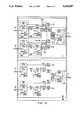
- FIG. 7shows a detailed schematic of the servologic circuit 40 according to the present invention.
- one half of the servologic circuitis shown which is used to generate the V cr and V cl control voltage signals, a second identical circuit being used for generating the V cf and V cb control voltage signals.
- the components in block 138, and the bias chain forming part of the threshold detector in block 140,are common to both circuits, however.
- the log ratio detector 61previously described in FIG. 4, receives signals LD and RD and produces a signal V LR at the output terminal 72. This terminal connects to the input terminal 120 of the servologic circuit 40, which is essentially organized according to the scheme of FIG. 6.
- Variable resistor element 122comprises two fixed resistors, R701 and R702, of 470K and 30K respectively, and switch S701, which may be one of four contained in industry standard part CD4066. This passes the signal at terminal 120 into capacitor 124 also labeled C701, which is typically 0.1 ⁇ F with the resistor values shown, thereby yielding a time constant that varies from 3 ms to 47 ms.
- the voltage on capacitor 124is buffered by operational amplifier OA701, connected as a voltage follower, which comprises non inverting unity gain buffer 126.
- the output of this bufferis connected to terminal 128 as control voltage V cr , and is also inverted by unity gain inverter 130.
- Thiscomprises two equal resistors R703, R704, connected as input and feedback resistors of an operational amplifier OA702 in inverting amplifier configuration.
- Amplifiers OA701 and OA702may typically be industry type TL074, having JFET inputs to minimize input current.
- the output of inverter 130is connected to terminal 132 as the second control voltage V cl .
- Summing rectifier circuit 134receives two inputs: from terminal 120, via resistor R705 to the virtual ground at the inverting input of operational amplifier OA703; and from terminal 132, via resistor R706 to the same point, resistors R705 and R706 being equal. This accomplishes a subtraction since the voltage at terminal 132 is precisely the negative of that across capacitor 124. Therefore, the net input current into operational amplifier OA703 is equal to the voltage across variable resistor element 122 divided by the 10K resistance of resistors R705 and R706.
- diode D701When this current is positive (i.e. flowing into the input of op-amp OA703), diode D701 conducts the same current to complete the feedback loop. Diode D702 is cut off, and as resistor R708 is connected to the virtual ground input of operational amplifier OA704, there is zero voltage across it or across resistor R707. An exactly equal current flows via the equal resistors R709 and R710 into the input of op-amp OA704, which has a feedback resistor R711 setting its gain to an appropriate value. The output voltage of op-amp OA704 therefore goes negative, and as the gain is -0.806, the output voltage is -0.806(V LR -V cr ).
- the output voltage of amplifier OA704is furthermore limited because this op-amp is supplied by ⁇ 7.5 V rails as shown in FIG. 4, being part of the same quad op-amp IC.
- This typehas been chosen because of its nearly symmetrical limiting characteristics. In practice, the negative supply to it is passed through an additional diode, not shown, to achieve this symmetrical limiting, thus making the negative supply to op-amp OA704 about -6.8 V.
- This output voltageis applied to the resistor control circuit 136, which is a width modulated pulse oscillator.
- the output of op-amp OA705is at about -14 V, close to the negative supply rail, and the non-inverting input is set to -0.2 V by the resistors R715 and R716.
- the voltage at the inverting inputis also slightly negative, set by the bias resistor R713 and resistor R714, working into resistor R712.
- the oscillator frequencytypically reaches about 20 kHz, yielding a duty ratio of about 0.08, It will be noted that the op-amp OA705 is being used as a comparator, and indeed a comparator such as industry type LM311 may be substituted therefor with improved speed characteristics.
- the frequency of oscillation of the pulse generatorincreases and so does the on time, until the duty ratio reaches 50%, and beyond this the frequency starts to fall again, but the duty ratio continues to increase, eventually reaching 100% when the current through the resistors R713 and R714 is insufficient to overcome the +0.2 V on the non inverting input. It is fairly easy to see that the duty ratio is a linear function of the input voltage over this range, but limits at a value of 1. Since about 280 ⁇ A is flowing in the bias resistors, the voltage across resistor R712 must be about 5.6 V, and therefore the circuit limits at an input of -5.4 V or so into resistor R712.
- the output of op-amp OA705is halved by equal resistors R717 and R718, so that it is suitable for application to the control input of switch S701, which is also supplied from ⁇ 7.5 V supply rails.
- the duty ratio dis less than 1, the total conductance is (2.13+33.2 d) ⁇ S, yielding an intermediate value of resistance between 28.3K and 470K.
- the resistance of element 122is varied according to the voltage across it in a suitable manner.
- the output of op-amp OA704also goes to a comparator circuit 140 employing op-amp OA706.
- a threshold voltage of -0.65 Vis set by resistors R719, R720, and when the negative voltage on the output of op-amp OA704 goes more negative than this, the output of op-amp OA706 switches to near the negative rail from its quiescent state near the positive rail. This causes diode D704 to conduct, pulling the voltage on resistor R721 of one-shot 138 negative.
- transistor Q701When this happens, transistor Q701 is switched off, causing transistor Q702 to receive base current through resistors R723 and R724. Timing capacitor C705 forces the base of transistor Q701 negative, providing positive feedback to ensure rapid switching. Because transistor Q701 is bipolar, the negative excursion may be limited by zener breakdown in this transistor.
- the one-shot 138releases after op-amp OA706 returns to its quiescent condition and capacitor C705 has recharged via resistor R722 to a point where transistor Q701 can turn on. This turns off transistor Q702, whose collector voltage rises with a time constant of 10 ms to the original value.
- transistor Q703When the one-shot 138 fires, transistor Q703 is also turned on, and the voltage at its collector goes to the -7.5 V rail. This voltage is transmitted via diode D703 to the input of oscillator 136, thereby forcing its output to positive limiting as long as the pulse continues and regardless of the difference voltage input. This reduces the time constant to its minimum value of 2.83 ⁇ s. With the values given, the pulse width will be about 20 ms after op-amp OA706 returns to normal and diode D704 is cut off. During this time, the difference voltage rapidly decreases, and so does the output voltage of op-amp OA704, thereby ensuring that the control voltage V cr reaches a level very close to V LR .
- the log ratio detector 62has inputs FD and BD, and processes the output signal V FB in exactly the same way.
- Resistors R719 and R720are shared with this circuit, which has a second comparator corresponding to op-amp OA706, whose inverting input is also connected to point X.
- This comparatoralso has a diode connected as for diode D704, with the cathode connected to point Y.
- the one-shot 138may thus be triggered on by either the left right or the front back servologic circuit.
- Point Zis connected to the diode corresponding with diode D703 in the other circuit, so that both PWM oscillators are forced to duty ratio of 1 when the one-shot 138 is fired. This ensures that all control voltages rapidly reach the appropriate values whenever either one has changed too fast for the one-shot to remain untriggered.
- the output of op-amp OA704is some function of this rate of change, and is therefore affected both by sudden changes in overall signal level, or "attacks", and by sudden changes in direction of the predominant sound (also usually caused by attacks when a new instrument or voice begins to be heard).
- the servologic circuit of FIG. 7also incorporates the one-shot 138 and its triggering mechanism, with all the advantages provided by this arrangement.
- the exact timingmay be varied by changing capacitor C705, if desired, and the threshold voltage may be altered by changing resistor R719.
- FIG. 8illustrates a filter circuit 800 which comprises a part of the variable matrix circuit 8.
- a filtermay be desirable in the rear channels to render the acoustic impression of some sound absorption and to reduce the possibility of sibilant "splash" in the rear of the listening room.
- resistor R801with the network comprising resistor R802 and capacitors C801 and C802, form a "pinking" filter with a slope of approximately 3 dB/octave above about 2 kHz. Resistor R803 and capacitor C803 provide a low frequency roll off below 200 Hz.
- the feedback resistor R804 around op-amp OA801defines the gain to be about -1.5 dB at 500 Hz.
- this filter circuitis applied in series with both rear channel signals LB, RB, after the separation matrix 8 itself, but possibly before the volume control and other similar functions such as generating the side channels' loudspeaker feed signals.
- An input signal LB applied to terminal 801will generate a modified output signal LB at terminal 802, having the frequency response characteristic shown in FIG. 9.
- a second filter(not shown) of this type may be used to modify the RB signal with the same frequency response characteristic.
- FIG. 9illustrates the output amplitude in decibels plotted against frequency in Hz for the filter of FIG. 8.
- FIG. 10illustrates a dual phase shifter circuit comprising two phase shifters 142, 144, which form part of the input conditioning matrix 6 of FIG. 1.
- the circuitreceives a monophonic input signal, which may be derived by averaging the left and right channel inputs, for example, as shown.
- the monophonic signalis passed through the two phase-shifters 142, 144 operating at different frequencies, thereby producing a phase difference between their outputs which varies from near zero at low frequencies to a maximum at mid frequencies, returning to near zero at high frequencies.
- the outputs of these two phase-shifters 142, 144become pseudo-stereo left and right channels to be applied to the remainder of the input matrixing circuitry 146 of block 6.
- the left channel phase shifter 142comprises resistors R101-R105, capacitor C101 and op-amp OA101.
- Resistors R101 and R102apply equal signals from each of terminals 2 and 4 to the inverting input of op-amp OA101, while resistors R104 and R105 apply equal signals from these terminals to capacitor C101.
- Feedback around op-amp OA101is provided by resistor R103.
- the phase shifter circuit 144is identical to that of the circuit 142, except that the capacitor C102 has a different value from capacitor C101. Therefore, the phase shifting effect occurs at a different frequency range, in this case over a range of frequencies about five times higher than for the phase shifter 142.
- phase shifters 142, 144are applied to the rest of the input conditioning circuits 146 forming part of the input conditioning matrix 6. These signals, labeled L' and R', are also applied to the inputs of the detector band pass filters 41, 42.
- FIG. 11shows the phase response characteristics of the two phase shifters 142, 144, and the third curve on this figure represents the phase difference between the outputs of these circuits.
- Phase shifter 142has its pole at 159 Hz
- phase shifter 144has its pole at 884 Hz.
- the maximum phase differenceis about 88 degrees at 375 Hz.
Landscapes
- Physics & Mathematics (AREA)
- Engineering & Computer Science (AREA)
- Acoustics & Sound (AREA)
- Signal Processing (AREA)
- Mathematical Analysis (AREA)
- General Physics & Mathematics (AREA)
- Algebra (AREA)
- Mathematical Optimization (AREA)
- Mathematical Physics (AREA)
- Pure & Applied Mathematics (AREA)
- Theoretical Computer Science (AREA)
- Stereophonic System (AREA)
- Amplifiers (AREA)
- Tone Control, Compression And Expansion, Limiting Amplitude (AREA)
Abstract
Description
c log (LD)-c log (RD)=c log (LD/RD) (1)
I=I.sub.s [exp (qV/nkT)-1] (2)
V=(nkT/q) ln (I/I.sub.s) (3)
δV=(nkT/q) ln (10)
=0.0592 n volts (4)
Claims (49)
Priority Applications (3)
| Application Number | Priority Date | Filing Date | Title |
|---|---|---|---|
| US07/789,529US5263087A (en) | 1990-06-08 | 1991-11-14 | Time constant processing circuit for surround processor |
| US07/983,645US5339363A (en) | 1990-06-08 | 1992-12-01 | Apparatus for enhancing monophonic audio signals using phase shifters |
| US07/983,689US5280528A (en) | 1990-06-08 | 1992-12-01 | Band pass filter circuit for rear channel filtering in a surround processor |
Applications Claiming Priority (3)
| Application Number | Priority Date | Filing Date | Title |
|---|---|---|---|
| US07/533,091US5172415A (en) | 1990-06-08 | 1990-06-08 | Surround processor |
| US07/789,529US5263087A (en) | 1990-06-08 | 1991-11-14 | Time constant processing circuit for surround processor |
| PCT/US1995/016897WO1997024012A1 (en) | 1990-06-08 | 1995-12-21 | Surround sound processor with improved control voltage generator |
Related Parent Applications (1)
| Application Number | Title | Priority Date | Filing Date |
|---|---|---|---|
| US07/533,091Continuation-In-PartUS5172415A (en) | 1990-06-08 | 1990-06-08 | Surround processor |
Related Child Applications (2)
| Application Number | Title | Priority Date | Filing Date |
|---|---|---|---|
| US07/983,689DivisionUS5280528A (en) | 1990-06-08 | 1992-12-01 | Band pass filter circuit for rear channel filtering in a surround processor |
| US07/983,645DivisionUS5339363A (en) | 1990-06-08 | 1992-12-01 | Apparatus for enhancing monophonic audio signals using phase shifters |
Publications (1)
| Publication Number | Publication Date |
|---|---|
| US5263087Atrue US5263087A (en) | 1993-11-16 |
Family
ID=56289237
Family Applications (4)
| Application Number | Title | Priority Date | Filing Date |
|---|---|---|---|
| US07/533,091Expired - LifetimeUS5172415A (en) | 1990-06-08 | 1990-06-08 | Surround processor |
| US07/789,529Expired - LifetimeUS5263087A (en) | 1990-06-08 | 1991-11-14 | Time constant processing circuit for surround processor |
| US07/967,446Expired - LifetimeUS5307415A (en) | 1990-06-08 | 1992-10-28 | Surround processor with antiphase blending and panorama control circuitry |
| US07/983,689Expired - LifetimeUS5280528A (en) | 1990-06-08 | 1992-12-01 | Band pass filter circuit for rear channel filtering in a surround processor |
Family Applications Before (1)
| Application Number | Title | Priority Date | Filing Date |
|---|---|---|---|
| US07/533,091Expired - LifetimeUS5172415A (en) | 1990-06-08 | 1990-06-08 | Surround processor |
Family Applications After (2)
| Application Number | Title | Priority Date | Filing Date |
|---|---|---|---|
| US07/967,446Expired - LifetimeUS5307415A (en) | 1990-06-08 | 1992-10-28 | Surround processor with antiphase blending and panorama control circuitry |
| US07/983,689Expired - LifetimeUS5280528A (en) | 1990-06-08 | 1992-12-01 | Band pass filter circuit for rear channel filtering in a surround processor |
Country Status (5)
| Country | Link |
|---|---|
| US (4) | US5172415A (en) |
| EP (1) | EP0533757B1 (en) |
| AU (1) | AU8097291A (en) |
| CA (1) | CA2084512A1 (en) |
| WO (2) | WO1991019407A1 (en) |
Cited By (21)
| Publication number | Priority date | Publication date | Assignee | Title |
|---|---|---|---|---|
| US5319713A (en)* | 1992-11-12 | 1994-06-07 | Rocktron Corporation | Multi dimensional sound circuit |
| US5428687A (en)* | 1990-06-08 | 1995-06-27 | James W. Fosgate | Control voltage generator multiplier and one-shot for integrated surround sound processor |
| US5504819A (en)* | 1990-06-08 | 1996-04-02 | Harman International Industries, Inc. | Surround sound processor with improved control voltage generator |
| US5530760A (en)* | 1994-04-29 | 1996-06-25 | Audio Products International Corp. | Apparatus and method for adjusting levels between channels of a sound system |
| WO1996033591A1 (en)* | 1995-04-21 | 1996-10-24 | Bsg Laboratories, Inc. | An acoustical audio system for producing three dimensional sound image |
| US5666424A (en)* | 1990-06-08 | 1997-09-09 | Harman International Industries, Inc. | Six-axis surround sound processor with automatic balancing and calibration |
| WO1997037512A1 (en)* | 1996-04-02 | 1997-10-09 | Harman International Industries, Inc. | Six-axis surround sound processor with improved matrix and cancellation control |
| US6587565B1 (en) | 1997-03-13 | 2003-07-01 | 3S-Tech Co., Ltd. | System for improving a spatial effect of stereo sound or encoded sound |
| US20050254446A1 (en)* | 2002-04-22 | 2005-11-17 | Breebaart Dirk J | Signal synthesizing |
| US20070059016A1 (en)* | 2005-09-12 | 2007-03-15 | Naoki Sato | Image forming apparatus |
| US7447321B2 (en) | 2001-05-07 | 2008-11-04 | Harman International Industries, Incorporated | Sound processing system for configuration of audio signals in a vehicle |
| US7451006B2 (en) | 2001-05-07 | 2008-11-11 | Harman International Industries, Incorporated | Sound processing system using distortion limiting techniques |
| US7466829B1 (en)* | 1999-08-24 | 2008-12-16 | Logitech Europe S.A. | Dynamic bass equalization with modified sallen-key high pass filter |
| US7492908B2 (en) | 2002-05-03 | 2009-02-17 | Harman International Industries, Incorporated | Sound localization system based on analysis of the sound field |
| US20090109166A1 (en)* | 2007-10-30 | 2009-04-30 | Sang-Gil Lee | Liquid crystal display and method of driving the same |
| US7760890B2 (en) | 2001-05-07 | 2010-07-20 | Harman International Industries, Incorporated | Sound processing system for configuration of audio signals in a vehicle |
| US20110164755A1 (en)* | 2008-09-03 | 2011-07-07 | Dolby Laboratories Licensing Corporation | Enhancing the Reproduction of Multiple Audio Channels |
| US8036402B2 (en) | 2005-12-15 | 2011-10-11 | Harman International Industries, Incorporated | Distortion compensation |
| WO2012078169A1 (en)* | 2010-12-10 | 2012-06-14 | Newport Corporation | Balanced light detector and related method |
| US9820073B1 (en) | 2017-05-10 | 2017-11-14 | Tls Corp. | Extracting a common signal from multiple audio signals |
| US20170372719A1 (en)* | 2016-06-22 | 2017-12-28 | Dolby Laboratories Licensing Corporation | Sibilance Detection and Mitigation |
Families Citing this family (81)
| Publication number | Priority date | Publication date | Assignee | Title |
|---|---|---|---|---|
| US6560341B1 (en)* | 1986-04-21 | 2003-05-06 | Jan R Coyle | System for transcription and playback of sonic signals |
| US5295189A (en)* | 1990-06-08 | 1994-03-15 | Fosgate James W | Control voltage generator for surround sound processor |
| JPH04265569A (en)* | 1991-02-19 | 1992-09-21 | Canon Inc | Sound signal recording device and reproducing device |
| US5757927A (en)* | 1992-03-02 | 1998-05-26 | Trifield Productions Ltd. | Surround sound apparatus |
| GB9204485D0 (en)* | 1992-03-02 | 1992-04-15 | Trifield Productions Ltd | Surround sound apparatus |
| US5333201A (en)* | 1992-11-12 | 1994-07-26 | Rocktron Corporation | Multi dimensional sound circuit |
| US5754664A (en)* | 1993-09-09 | 1998-05-19 | Prince Corporation | Vehicle audio system |
| US6240189B1 (en)* | 1994-06-08 | 2001-05-29 | Bose Corporation | Generating a common bass signal |
| JP2876993B2 (en)* | 1994-07-07 | 1999-03-31 | ヤマハ株式会社 | Reproduction characteristic control device |
| DE4440014C2 (en)* | 1994-11-09 | 2002-02-07 | Deutsche Telekom Ag | Method and device for multi-channel sound reproduction |
| US5661808A (en)* | 1995-04-27 | 1997-08-26 | Srs Labs, Inc. | Stereo enhancement system |
| US5850453A (en)* | 1995-07-28 | 1998-12-15 | Srs Labs, Inc. | Acoustic correction apparatus |
| JP2766466B2 (en)* | 1995-08-02 | 1998-06-18 | 株式会社東芝 | Audio system, reproduction method, recording medium and recording method on recording medium |
| KR0128064Y1 (en)* | 1995-08-18 | 1998-11-02 | 김광호 | Surround sound signal playback device with subwoofer signal synthesis |
| US5771295A (en)* | 1995-12-26 | 1998-06-23 | Rocktron Corporation | 5-2-5 matrix system |
| US5841993A (en)* | 1996-01-02 | 1998-11-24 | Ho; Lawrence | Surround sound system for personal computer for interfacing surround sound with personal computer |
| US5883961A (en)* | 1996-01-26 | 1999-03-16 | Harman International Industries, Incorporated | Sound system |
| US5970152A (en)* | 1996-04-30 | 1999-10-19 | Srs Labs, Inc. | Audio enhancement system for use in a surround sound environment |
| US6697491B1 (en) | 1996-07-19 | 2004-02-24 | Harman International Industries, Incorporated | 5-2-5 matrix encoder and decoder system |
| FR2751828A1 (en)* | 1996-07-24 | 1998-01-30 | Guisto Marc Albert | Surround sound decoder converter system for home cinemas |
| DE19646055A1 (en)* | 1996-11-07 | 1998-05-14 | Thomson Brandt Gmbh | Method and device for mapping sound sources onto loudspeakers |
| US5912976A (en) | 1996-11-07 | 1999-06-15 | Srs Labs, Inc. | Multi-channel audio enhancement system for use in recording and playback and methods for providing same |
| US6711266B1 (en) | 1997-02-07 | 2004-03-23 | Bose Corporation | Surround sound channel encoding and decoding |
| US6281749B1 (en) | 1997-06-17 | 2001-08-28 | Srs Labs, Inc. | Sound enhancement system |
| WO1998058523A1 (en)* | 1997-06-17 | 1998-12-23 | British Telecommunications Public Limited Company | Reproduction of spatialised audio |
| PL338988A1 (en)* | 1997-09-05 | 2000-12-04 | Lexicon | Matrix-type 5-2-5 encoder and decoder system |
| KR100454012B1 (en)* | 1997-09-05 | 2004-10-26 | 하만인터내셔날인더스트리스인코포레이티드 | 5-2-5 matrix encoder and decoder system |
| AU2202299A (en)* | 1997-12-23 | 1999-07-12 | Lexicon | Method and system for driving speakers with a 90 degree phase shift |
| US6683962B1 (en) | 1997-12-23 | 2004-01-27 | Harman International Industries, Incorporated | Method and system for driving speakers with a 90 degree phase shift |
| US7085710B1 (en)* | 1998-01-07 | 2006-08-01 | Microsoft Corporation | Vehicle computer system audio entertainment system |
| US6038330A (en)* | 1998-02-20 | 2000-03-14 | Meucci, Jr.; Robert James | Virtual sound headset and method for simulating spatial sound |
| EP1070417B1 (en)* | 1998-04-08 | 2002-09-18 | BRITISH TELECOMMUNICATIONS public limited company | Echo cancellation |
| EP0950956A1 (en) | 1998-04-17 | 1999-10-20 | BRITISH TELECOMMUNICATIONS public limited company | Computer network |
| US6555042B1 (en) | 1998-07-24 | 2003-04-29 | Lear Corporation | Method of making a vehicle headliner assembly with integral speakers |
| US6694027B1 (en) | 1999-03-09 | 2004-02-17 | Smart Devices, Inc. | Discrete multi-channel/5-2-5 matrix system |
| US7149313B1 (en)* | 1999-05-17 | 2006-12-12 | Bose Corporation | Audio signal processing |
| US7031474B1 (en) | 1999-10-04 | 2006-04-18 | Srs Labs, Inc. | Acoustic correction apparatus |
| US6920223B1 (en) | 1999-12-03 | 2005-07-19 | Dolby Laboratories Licensing Corporation | Method for deriving at least three audio signals from two input audio signals |
| US6970567B1 (en) | 1999-12-03 | 2005-11-29 | Dolby Laboratories Licensing Corporation | Method and apparatus for deriving at least one audio signal from two or more input audio signals |
| US7277767B2 (en) | 1999-12-10 | 2007-10-02 | Srs Labs, Inc. | System and method for enhanced streaming audio |
| US7212872B1 (en)* | 2000-05-10 | 2007-05-01 | Dts, Inc. | Discrete multichannel audio with a backward compatible mix |
| US7298852B2 (en)* | 2001-07-11 | 2007-11-20 | American Technology Corporation | Dynamic power sharing in a multi-channel sound system |
| JP2004511927A (en)* | 2000-07-11 | 2004-04-15 | アメリカン・テクノロジー・コーポレーション | Power amplifier for parametric speakers |
| CN1307853C (en)* | 2000-08-31 | 2007-03-28 | 杜比实验特许公司 | Method for appts. for audio matrix decoding |
| JP4716238B2 (en)* | 2000-09-27 | 2011-07-06 | 日本電気株式会社 | Sound reproduction system and method for portable terminal device |
| US7003467B1 (en)* | 2000-10-06 | 2006-02-21 | Digital Theater Systems, Inc. | Method of decoding two-channel matrix encoded audio to reconstruct multichannel audio |
| DE10110422A1 (en)* | 2001-03-05 | 2002-09-19 | Harman Becker Automotive Sys | Method for controlling a multi-channel sound reproduction system and multi-channel sound reproduction system |
| FR2836571B1 (en)* | 2002-02-28 | 2004-07-09 | Remy Henri Denis Bruno | METHOD AND DEVICE FOR DRIVING AN ACOUSTIC FIELD RESTITUTION ASSEMBLY |
| US20040086130A1 (en)* | 2002-05-03 | 2004-05-06 | Eid Bradley F. | Multi-channel sound processing systems |
| US20040081323A1 (en)* | 2002-10-28 | 2004-04-29 | Charles Sung | Noise-suppression earphone |
| US7218745B2 (en)* | 2002-12-23 | 2007-05-15 | Lear Corporation | Headliner transducer covers |
| US20050185806A1 (en)* | 2003-02-14 | 2005-08-25 | Salvador Eduardo T. | Controlling fading and surround signal level |
| GB2410164A (en)* | 2004-01-16 | 2005-07-20 | Anthony John Andrews | Sound feature positioner |
| EP1721312B1 (en)* | 2004-03-01 | 2008-03-26 | Dolby Laboratories Licensing Corporation | Multichannel audio coding |
| US7106411B2 (en)* | 2004-05-05 | 2006-09-12 | Imax Corporation | Conversion of cinema theatre to a super cinema theatre |
| SG124306A1 (en)* | 2005-01-20 | 2006-08-30 | St Microelectronics Asia | A system and method for expanding multi-speaker playback |
| JP4418774B2 (en)* | 2005-05-13 | 2010-02-24 | アルパイン株式会社 | Audio apparatus and surround sound generation method |
| US8619998B2 (en)* | 2006-08-07 | 2013-12-31 | Creative Technology Ltd | Spatial audio enhancement processing method and apparatus |
| US7933324B2 (en)* | 2006-05-31 | 2011-04-26 | Lear Corporation | Power regulator |
| JP5485693B2 (en) | 2006-08-10 | 2014-05-07 | コーニンクレッカ フィリップス エヌ ヴェ | Apparatus and method for processing audio signals |
| US20080139312A1 (en)* | 2006-12-08 | 2008-06-12 | Aruze Gaming America, Inc. | Gaming machine and volume control method thereof |
| US20080139313A1 (en)* | 2006-12-08 | 2008-06-12 | Aruze Gaming America, Inc. | Gaming machine and volume control method thereof |
| US8050434B1 (en) | 2006-12-21 | 2011-11-01 | Srs Labs, Inc. | Multi-channel audio enhancement system |
| JP5213339B2 (en)* | 2007-03-12 | 2013-06-19 | アルパイン株式会社 | Audio equipment |
| JP5355387B2 (en)* | 2007-03-30 | 2013-11-27 | パナソニック株式会社 | Encoding apparatus and encoding method |
| US20080305872A1 (en)* | 2007-06-07 | 2008-12-11 | Aruze Gaming America Inc. | Gaming machine adjusting the volume level of background music |
| US20080305857A1 (en)* | 2007-06-07 | 2008-12-11 | Aruze Gaming America, Inc. | Gaming machine capable of changing the volume level in the predetermined audio range and tone control method |
| TW201025841A (en)* | 2008-12-31 | 2010-07-01 | Princeton Technology Corp | Loudness circuit without operational amplifier |
| US20100310100A1 (en)* | 2009-06-03 | 2010-12-09 | International Truck Intellectual Property Company, Llc | Loudspeaker input switch system to reorient sound in truck |
| US8259960B2 (en)* | 2009-09-11 | 2012-09-04 | BSG Laboratory, LLC | Phase layering apparatus and method for a complete audio signal |
| US20120155650A1 (en)* | 2010-12-15 | 2012-06-21 | Harman International Industries, Incorporated | Speaker array for virtual surround rendering |
| US9154897B2 (en) | 2011-01-04 | 2015-10-06 | Dts Llc | Immersive audio rendering system |
| WO2013032822A2 (en) | 2011-08-26 | 2013-03-07 | Dts Llc | Audio adjustment system |
| WO2014046941A1 (en) | 2012-09-19 | 2014-03-27 | Dolby Laboratories Licensing Corporation | Method and system for object-dependent adjustment of levels of audio objects |
| US10149058B2 (en) | 2013-03-15 | 2018-12-04 | Richard O'Polka | Portable sound system |
| US9084047B2 (en) | 2013-03-15 | 2015-07-14 | Richard O'Polka | Portable sound system |
| WO2014190140A1 (en) | 2013-05-23 | 2014-11-27 | Alan Kraemer | Headphone audio enhancement system |
| USD740784S1 (en) | 2014-03-14 | 2015-10-13 | Richard O'Polka | Portable sound device |
| US10078612B2 (en)* | 2014-07-28 | 2018-09-18 | Intel Corporation | Mode selective balanced encoded interconnect |
| FR3032073B1 (en)* | 2015-01-22 | 2017-02-10 | Continental Automotive France | DEVICE FOR PROCESSING AN AUDIO SIGNAL |
| US10862446B2 (en) | 2018-04-02 | 2020-12-08 | Sonos, Inc. | Systems and methods of volume limiting |
Citations (14)
| Publication number | Priority date | Publication date | Assignee | Title |
|---|---|---|---|---|
| US3632886A (en)* | 1969-12-29 | 1972-01-04 | Peter Scheiber | Quadrasonic sound system |
| US3708631A (en)* | 1970-06-08 | 1973-01-02 | Columbia Broadcasting Syst Inc | Quadraphonic reproducing system with gain control |
| US3746792A (en)* | 1968-01-11 | 1973-07-17 | P Scheiber | Multidirectional sound system |
| US3836715A (en)* | 1972-09-09 | 1974-09-17 | Sansui Electric Co | Decoder for use in 4-2-4 matrix playback system |
| US3864516A (en)* | 1972-03-07 | 1975-02-04 | Tokyo Shibaura Electric Co | Four-Channel Stereophonic Sound Reproducing System |
| US3883832A (en)* | 1972-11-06 | 1975-05-13 | James Wayne Fosgate | Single element controlled parallel-T audio network |
| US3883692A (en)* | 1972-06-16 | 1975-05-13 | Sony Corp | Decoder apparatus with logic circuit for use with a four channel stereo |
| US3885099A (en)* | 1972-12-01 | 1975-05-20 | Sony Corp | Integrated logic circuit for the decoder of a multi-channel stereo apparatus |
| US3943287A (en)* | 1974-06-03 | 1976-03-09 | Cbs Inc. | Apparatus and method for decoding four channel sound |
| US3944735A (en)* | 1974-03-25 | 1976-03-16 | John C. Bogue | Directional enhancement system for quadraphonic decoders |
| US3959590A (en)* | 1969-01-11 | 1976-05-25 | Peter Scheiber | Stereophonic sound system |
| US4704728A (en)* | 1984-12-31 | 1987-11-03 | Peter Scheiber | Signal re-distribution, decoding and processing in accordance with amplitude, phase, and other characteristics |
| US4932059A (en)* | 1988-01-11 | 1990-06-05 | Fosgate Inc. | Variable matrix decoder for periphonic reproduction of sound |
| US5046098A (en)* | 1985-03-07 | 1991-09-03 | Dolby Laboratories Licensing Corporation | Variable matrix decoder with three output channels |
Family Cites Families (8)
| Publication number | Priority date | Publication date | Assignee | Title |
|---|---|---|---|---|
| GB1402320A (en)* | 1971-10-25 | 1975-08-06 | Sansui Electric Co | Decoder for use in 4-2-4 matrix playback system |
| JPS5527760B2 (en)* | 1973-05-10 | 1980-07-23 | ||
| US3982071A (en)* | 1974-08-20 | 1976-09-21 | Weiss Edward A | Multichannel sound signal processing system employing voltage controlled amplifiers |
| JPS5577213A (en)* | 1978-12-06 | 1980-06-10 | Fujitsu Ten Ltd | Selective amplifier |
| US4706287A (en)* | 1984-10-17 | 1987-11-10 | Kintek, Inc. | Stereo generator |
| US4799260A (en)* | 1985-03-07 | 1989-01-17 | Dolby Laboratories Licensing Corporation | Variable matrix decoder |
| FR2631505B1 (en)* | 1988-05-11 | 1990-08-31 | Neiman Sa | DEVICE FOR POWERING A LOUDSPEAKER OF ACOUSTIC SIGNALING |
| US5216718A (en)* | 1990-04-26 | 1993-06-01 | Sanyo Electric Co., Ltd. | Method and apparatus for processing audio signals |
- 1990
- 1990-06-08USUS07/533,091patent/US5172415A/ennot_activeExpired - Lifetime
- 1991
- 1991-06-05CACA002084512Apatent/CA2084512A1/ennot_activeAbandoned
- 1991-06-05AUAU80972/91Apatent/AU8097291A/ennot_activeAbandoned
- 1991-06-05WOPCT/US1991/003950patent/WO1991019407A1/enactiveIP Right Grant
- 1991-06-05EPEP91910951Apatent/EP0533757B1/ennot_activeExpired - Lifetime
- 1991-11-14USUS07/789,529patent/US5263087A/ennot_activeExpired - Lifetime
- 1992
- 1992-10-28USUS07/967,446patent/US5307415A/ennot_activeExpired - Lifetime
- 1992-12-01USUS07/983,689patent/US5280528A/ennot_activeExpired - Lifetime
- 1995
- 1995-12-21WOPCT/US1995/016897patent/WO1997024012A1/enactiveIP Right Grant
Patent Citations (15)
| Publication number | Priority date | Publication date | Assignee | Title |
|---|---|---|---|---|
| US3746792A (en)* | 1968-01-11 | 1973-07-17 | P Scheiber | Multidirectional sound system |
| US3959590A (en)* | 1969-01-11 | 1976-05-25 | Peter Scheiber | Stereophonic sound system |
| US3632886A (en)* | 1969-12-29 | 1972-01-04 | Peter Scheiber | Quadrasonic sound system |
| US3708631A (en)* | 1970-06-08 | 1973-01-02 | Columbia Broadcasting Syst Inc | Quadraphonic reproducing system with gain control |
| US3864516A (en)* | 1972-03-07 | 1975-02-04 | Tokyo Shibaura Electric Co | Four-Channel Stereophonic Sound Reproducing System |
| US3883692A (en)* | 1972-06-16 | 1975-05-13 | Sony Corp | Decoder apparatus with logic circuit for use with a four channel stereo |
| US3836715A (en)* | 1972-09-09 | 1974-09-17 | Sansui Electric Co | Decoder for use in 4-2-4 matrix playback system |
| US3883832A (en)* | 1972-11-06 | 1975-05-13 | James Wayne Fosgate | Single element controlled parallel-T audio network |
| US3885099A (en)* | 1972-12-01 | 1975-05-20 | Sony Corp | Integrated logic circuit for the decoder of a multi-channel stereo apparatus |
| US3944735A (en)* | 1974-03-25 | 1976-03-16 | John C. Bogue | Directional enhancement system for quadraphonic decoders |
| US3943287A (en)* | 1974-06-03 | 1976-03-09 | Cbs Inc. | Apparatus and method for decoding four channel sound |
| US4704728A (en)* | 1984-12-31 | 1987-11-03 | Peter Scheiber | Signal re-distribution, decoding and processing in accordance with amplitude, phase, and other characteristics |
| US4891839A (en)* | 1984-12-31 | 1990-01-02 | Peter Scheiber | Signal re-distribution, decoding and processing in accordance with amplitude, phase and other characteristics |
| US5046098A (en)* | 1985-03-07 | 1991-09-03 | Dolby Laboratories Licensing Corporation | Variable matrix decoder with three output channels |
| US4932059A (en)* | 1988-01-11 | 1990-06-05 | Fosgate Inc. | Variable matrix decoder for periphonic reproduction of sound |
Cited By (38)
| Publication number | Priority date | Publication date | Assignee | Title |
|---|---|---|---|---|
| US5428687A (en)* | 1990-06-08 | 1995-06-27 | James W. Fosgate | Control voltage generator multiplier and one-shot for integrated surround sound processor |
| US5504819A (en)* | 1990-06-08 | 1996-04-02 | Harman International Industries, Inc. | Surround sound processor with improved control voltage generator |
| US5644640A (en)* | 1990-06-08 | 1997-07-01 | Harman International Industries, Inc. | Surround sound processor with improved control voltage generator |
| US5666424A (en)* | 1990-06-08 | 1997-09-09 | Harman International Industries, Inc. | Six-axis surround sound processor with automatic balancing and calibration |
| US5319713A (en)* | 1992-11-12 | 1994-06-07 | Rocktron Corporation | Multi dimensional sound circuit |
| US5530760A (en)* | 1994-04-29 | 1996-06-25 | Audio Products International Corp. | Apparatus and method for adjusting levels between channels of a sound system |
| WO1996033591A1 (en)* | 1995-04-21 | 1996-10-24 | Bsg Laboratories, Inc. | An acoustical audio system for producing three dimensional sound image |
| WO1997037512A1 (en)* | 1996-04-02 | 1997-10-09 | Harman International Industries, Inc. | Six-axis surround sound processor with improved matrix and cancellation control |
| ES2152870A1 (en)* | 1996-04-02 | 2001-02-01 | Harman Int Ind | Six-axis surround sound processor with improved matrix and cancellation control |
| US6587565B1 (en) | 1997-03-13 | 2003-07-01 | 3S-Tech Co., Ltd. | System for improving a spatial effect of stereo sound or encoded sound |
| US8565448B2 (en) | 1999-08-24 | 2013-10-22 | Logitech Europe S.A. | Dynamic bass equalization with modified Sallen-Key high pass filter |
| US7466829B1 (en)* | 1999-08-24 | 2008-12-16 | Logitech Europe S.A. | Dynamic bass equalization with modified sallen-key high pass filter |
| US7760890B2 (en) | 2001-05-07 | 2010-07-20 | Harman International Industries, Incorporated | Sound processing system for configuration of audio signals in a vehicle |
| US7447321B2 (en) | 2001-05-07 | 2008-11-04 | Harman International Industries, Incorporated | Sound processing system for configuration of audio signals in a vehicle |
| US7451006B2 (en) | 2001-05-07 | 2008-11-11 | Harman International Industries, Incorporated | Sound processing system using distortion limiting techniques |
| US8472638B2 (en) | 2001-05-07 | 2013-06-25 | Harman International Industries, Incorporated | Sound processing system for configuration of audio signals in a vehicle |
| US8031879B2 (en) | 2001-05-07 | 2011-10-04 | Harman International Industries, Incorporated | Sound processing system using spatial imaging techniques |
| US8798275B2 (en) | 2002-04-22 | 2014-08-05 | Koninklijke Philips N.V. | Signal synthesizing |
| US7933415B2 (en)* | 2002-04-22 | 2011-04-26 | Koninklijke Philips Electronics N.V. | Signal synthesizing |
| US20110166866A1 (en)* | 2002-04-22 | 2011-07-07 | Koninklijke Philips Electronics N.V. | Signal synthesizing |
| US20050254446A1 (en)* | 2002-04-22 | 2005-11-17 | Breebaart Dirk J | Signal synthesizing |
| US7492908B2 (en) | 2002-05-03 | 2009-02-17 | Harman International Industries, Incorporated | Sound localization system based on analysis of the sound field |
| US7567676B2 (en) | 2002-05-03 | 2009-07-28 | Harman International Industries, Incorporated | Sound event detection and localization system using power analysis |
| US7499553B2 (en) | 2002-05-03 | 2009-03-03 | Harman International Industries Incorporated | Sound event detector system |
| US8736861B2 (en)* | 2005-09-12 | 2014-05-27 | Ricoh Company, Ltd. | Image forming apparatus |
| US9213297B2 (en) | 2005-09-12 | 2015-12-15 | Ricoh Company, Ltd. | Image forming apparatus |
| US20070059016A1 (en)* | 2005-09-12 | 2007-03-15 | Naoki Sato | Image forming apparatus |
| US8942391B2 (en) | 2005-12-15 | 2015-01-27 | Harman International Industries, Incorporated | Distortion compensation |
| US8036402B2 (en) | 2005-12-15 | 2011-10-11 | Harman International Industries, Incorporated | Distortion compensation |
| US20090109166A1 (en)* | 2007-10-30 | 2009-04-30 | Sang-Gil Lee | Liquid crystal display and method of driving the same |
| US9014378B2 (en) | 2008-09-03 | 2015-04-21 | Dolby Laboratories Licensing Corporation | Enhancing the reproduction of multiple audio channels |
| US20110164755A1 (en)* | 2008-09-03 | 2011-07-07 | Dolby Laboratories Licensing Corporation | Enhancing the Reproduction of Multiple Audio Channels |
| US9706308B2 (en) | 2008-09-03 | 2017-07-11 | Dolby Laboratories Licensing Corporation | Enhancing the reproduction of multiple audio channels |
| US10356528B2 (en) | 2008-09-03 | 2019-07-16 | Dolby Laboratories Licensing Corporation | Enhancing the reproduction of multiple audio channels |
| WO2012078169A1 (en)* | 2010-12-10 | 2012-06-14 | Newport Corporation | Balanced light detector and related method |
| US20170372719A1 (en)* | 2016-06-22 | 2017-12-28 | Dolby Laboratories Licensing Corporation | Sibilance Detection and Mitigation |
| US10867620B2 (en)* | 2016-06-22 | 2020-12-15 | Dolby Laboratories Licensing Corporation | Sibilance detection and mitigation |
| US9820073B1 (en) | 2017-05-10 | 2017-11-14 | Tls Corp. | Extracting a common signal from multiple audio signals |
Also Published As
| Publication number | Publication date |
|---|---|
| EP0533757B1 (en) | 1998-09-09 |
| US5307415A (en) | 1994-04-26 |
| WO1991019407A1 (en) | 1991-12-12 |
| CA2084512A1 (en) | 1991-12-09 |
| AU8097291A (en) | 1991-12-31 |
| EP0533757A1 (en) | 1993-03-31 |
| EP0533757A4 (en) | 1993-08-11 |
| US5172415A (en) | 1992-12-15 |
| US5280528A (en) | 1994-01-18 |
| WO1997024012A1 (en) | 1997-07-03 |
Similar Documents
| Publication | Publication Date | Title |
|---|---|---|
| US5263087A (en) | Time constant processing circuit for surround processor | |
| US5339363A (en) | Apparatus for enhancing monophonic audio signals using phase shifters | |
| US5530760A (en) | Apparatus and method for adjusting levels between channels of a sound system | |
| JP2642209B2 (en) | System and method for generating output signal with enhanced stereo sound effect from monaural input signal | |
| US4984273A (en) | Enhancing bass | |
| US5610986A (en) | Linear-matrix audio-imaging system and image analyzer | |
| KR100458021B1 (en) | Multi-channel audio enhancement system for use in recording and playback and methods for providing same | |
| JP2824642B2 (en) | Variable matrix decoder | |
| EP0276948B1 (en) | Sound field control device | |
| US4308424A (en) | Simulated stereo from a monaural source sound reproduction system | |
| US3708631A (en) | Quadraphonic reproducing system with gain control | |
| US4612663A (en) | Multichannel audio reproduction system | |
| EP0677235B1 (en) | Sound image manipulation apparatus for sound image enhancement | |
| JPS6337560B2 (en) | ||
| US5625696A (en) | Six-axis surround sound processor with improved matrix and cancellation control | |
| US5295189A (en) | Control voltage generator for surround sound processor | |
| US3046337A (en) | Stereophonic sound | |
| US3812295A (en) | Quadraphonic reproducing system with gain riding logic | |
| US4443889A (en) | Acoustic apparatus and method | |
| CA2098319C (en) | Signal processor for recreating original audio signals | |
| JPH06500898A (en) | surround processor | |
| US3794780A (en) | Quadraphonic recording system | |
| JPH0638300A (en) | Acoustic reproduction equipment | |
| JPH05161199A (en) | Audio equipment | |
| HK1025868B (en) | Six-axis surround sound processor with improved matrix and cancellation control |
Legal Events
| Date | Code | Title | Description |
|---|---|---|---|
| STCF | Information on status: patent grant | Free format text:PATENTED CASE | |
| AS | Assignment | Owner name:HARMAN INTERNATIONAL INDUSTRIES, INC., CALIFORNIA Free format text:EXCLUSIVE LICENSE AGREEMENT;ASSIGNOR:FOSGATE, JAMES W.;REEL/FRAME:007038/0184 Effective date:19910131 | |
| CC | Certificate of correction | ||
| FPAY | Fee payment | Year of fee payment:4 | |
| FPAY | Fee payment | Year of fee payment:8 | |
| REMI | Maintenance fee reminder mailed | ||
| FPAY | Fee payment | Year of fee payment:12 | |
| SULP | Surcharge for late payment | Year of fee payment:11 | |
| AS | Assignment | Owner name:JPMORGAN CHASE BANK, N.A., NEW YORK Free format text:SECURITY AGREEMENT;ASSIGNORS:HARMAN INTERNATIONAL INDUSTRIES, INCORPORATED;BECKER SERVICE-UND VERWALTUNG GMBH;CROWN AUDIO, INC.;AND OTHERS;REEL/FRAME:022659/0743 Effective date:20090331 Owner name:JPMORGAN CHASE BANK, N.A.,NEW YORK Free format text:SECURITY AGREEMENT;ASSIGNORS:HARMAN INTERNATIONAL INDUSTRIES, INCORPORATED;BECKER SERVICE-UND VERWALTUNG GMBH;CROWN AUDIO, INC.;AND OTHERS;REEL/FRAME:022659/0743 Effective date:20090331 | |
| AS | Assignment | Owner name:HARMAN INTERNATIONAL INDUSTRIES, INCORPORATED, CON Free format text:RELEASE;ASSIGNOR:JPMORGAN CHASE BANK, N.A., AS ADMINISTRATIVE AGENT;REEL/FRAME:025795/0143 Effective date:20101201 Owner name:HARMAN BECKER AUTOMOTIVE SYSTEMS GMBH, CONNECTICUT Free format text:RELEASE;ASSIGNOR:JPMORGAN CHASE BANK, N.A., AS ADMINISTRATIVE AGENT;REEL/FRAME:025795/0143 Effective date:20101201 | |
| AS | Assignment | Owner name:JPMORGAN CHASE BANK, N.A., AS ADMINISTRATIVE AGENT Free format text:SECURITY AGREEMENT;ASSIGNORS:HARMAN INTERNATIONAL INDUSTRIES, INCORPORATED;HARMAN BECKER AUTOMOTIVE SYSTEMS GMBH;REEL/FRAME:025823/0354 Effective date:20101201 | |
| AS | Assignment | Owner name:HARMAN INTERNATIONAL INDUSTRIES, INCORPORATED, CON Free format text:RELEASE;ASSIGNOR:JPMORGAN CHASE BANK, N.A., AS ADMINISTRATIVE AGENT;REEL/FRAME:029294/0254 Effective date:20121010 Owner name:HARMAN BECKER AUTOMOTIVE SYSTEMS GMBH, CONNECTICUT Free format text:RELEASE;ASSIGNOR:JPMORGAN CHASE BANK, N.A., AS ADMINISTRATIVE AGENT;REEL/FRAME:029294/0254 Effective date:20121010 |