US5262754A - Overvoltage protection element - Google Patents
Overvoltage protection elementDownload PDFInfo
- Publication number
- US5262754A US5262754AUS07/949,709US94970992AUS5262754AUS 5262754 AUS5262754 AUS 5262754AUS 94970992 AUS94970992 AUS 94970992AUS 5262754 AUS5262754 AUS 5262754A
- Authority
- US
- United States
- Prior art keywords
- overvoltage protection
- protection element
- spaced
- sheet
- major surfaces
- Prior art date
- Legal status (The legal status is an assumption and is not a legal conclusion. Google has not performed a legal analysis and makes no representation as to the accuracy of the status listed.)
- Expired - Lifetime
Links
- 239000000463materialSubstances0.000claimsabstractdescription40
- 239000011810insulating materialSubstances0.000claimsabstractdescription4
- 239000011230binding agentSubstances0.000claimsdescription7
- 239000002245particleSubstances0.000claimsdescription5
- 229920001971elastomerPolymers0.000claimsdescription3
- 229920000642polymerPolymers0.000claimsdescription3
- 239000004593EpoxySubstances0.000claimsdescription2
- 230000015556catabolic processEffects0.000claimsdescription2
- 239000000919ceramicSubstances0.000claimsdescription2
- 239000000806elastomerSubstances0.000claimsdescription2
- 125000003700epoxy groupChemical group0.000claimsdescription2
- 239000011521glassSubstances0.000claimsdescription2
- 229920000647polyepoxidePolymers0.000claimsdescription2
- 229920001187thermosetting polymerPolymers0.000claimsdescription2
- 230000005641tunnelingEffects0.000claimsdescription2
- ZHPNWZCWUUJAJC-UHFFFAOYSA-NfluorosiliconChemical compound[Si]FZHPNWZCWUUJAJC-UHFFFAOYSA-N0.000claims1
- 239000005060rubberSubstances0.000claims1
- 229910052710siliconInorganic materials0.000claims1
- 239000010703siliconSubstances0.000claims1
- 229920001169thermoplasticPolymers0.000claims1
- 239000004416thermosoftening plasticSubstances0.000claims1
- 239000004020conductorSubstances0.000description8
- 238000000034methodMethods0.000description7
- 239000011159matrix materialSubstances0.000description5
- -1polyethylenePolymers0.000description3
- 238000003490calenderingMethods0.000description2
- 238000000465mouldingMethods0.000description2
- 238000003825pressingMethods0.000description2
- 238000005096rolling processMethods0.000description2
- 239000000758substrateSubstances0.000description2
- 239000004698PolyethyleneSubstances0.000description1
- 239000004743PolypropyleneSubstances0.000description1
- 239000002253acidSubstances0.000description1
- 239000000853adhesiveSubstances0.000description1
- 230000001070adhesive effectEffects0.000description1
- 238000003486chemical etchingMethods0.000description1
- 239000011248coating agentSubstances0.000description1
- 238000000576coating methodMethods0.000description1
- 238000005520cutting processMethods0.000description1
- 230000000254damaging effectEffects0.000description1
- 230000001419dependent effectEffects0.000description1
- 238000007598dipping methodMethods0.000description1
- 239000012777electrically insulating materialSubstances0.000description1
- 239000004744fabricSubstances0.000description1
- 238000010030laminatingMethods0.000description1
- 238000004519manufacturing processMethods0.000description1
- 239000002184metalSubstances0.000description1
- 229920003052natural elastomerPolymers0.000description1
- 229920001194natural rubberPolymers0.000description1
- 238000010422paintingMethods0.000description1
- 229920000728polyesterPolymers0.000description1
- 229920000573polyethylenePolymers0.000description1
- 229920001155polypropylenePolymers0.000description1
- 238000012545processingMethods0.000description1
- 238000004080punchingMethods0.000description1
- 229920005989resinPolymers0.000description1
- 239000011347resinSubstances0.000description1
- 229920002379silicone rubberPolymers0.000description1
- 229920003051synthetic elastomerPolymers0.000description1
- 239000005061synthetic rubberSubstances0.000description1
- 239000012815thermoplastic materialSubstances0.000description1
- 230000001052transient effectEffects0.000description1
Images


Classifications
- H—ELECTRICITY
- H01—ELECTRIC ELEMENTS
- H01C—RESISTORS
- H01C7/00—Non-adjustable resistors formed as one or more layers or coatings; Non-adjustable resistors made from powdered conducting material or powdered semi-conducting material with or without insulating material
- H01C7/10—Non-adjustable resistors formed as one or more layers or coatings; Non-adjustable resistors made from powdered conducting material or powdered semi-conducting material with or without insulating material voltage responsive, i.e. varistors
- H01C7/105—Varistor cores
- H—ELECTRICITY
- H05—ELECTRIC TECHNIQUES NOT OTHERWISE PROVIDED FOR
- H05K—PRINTED CIRCUITS; CASINGS OR CONSTRUCTIONAL DETAILS OF ELECTRIC APPARATUS; MANUFACTURE OF ASSEMBLAGES OF ELECTRICAL COMPONENTS
- H05K1/00—Printed circuits
- H05K1/02—Details
- H05K1/0213—Electrical arrangements not otherwise provided for
- H05K1/0254—High voltage adaptations; Electrical insulation details; Overvoltage or electrostatic discharge protection ; Arrangements for regulating voltages or for using plural voltages
- H—ELECTRICITY
- H05—ELECTRIC TECHNIQUES NOT OTHERWISE PROVIDED FOR
- H05K—PRINTED CIRCUITS; CASINGS OR CONSTRUCTIONAL DETAILS OF ELECTRIC APPARATUS; MANUFACTURE OF ASSEMBLAGES OF ELECTRICAL COMPONENTS
- H05K1/00—Printed circuits
- H05K1/18—Printed circuits structurally associated with non-printed electric components
- H05K1/181—Printed circuits structurally associated with non-printed electric components associated with surface mounted components
Definitions
- This inventionrelates generally to an overvoltage protection element, and more particularly to an overvoltage protection element which can replace discrete devices presently used in protecting electronic circuits from disruptive and/or damaging effects of overvoltage transients.
- non-linear materialmaterials having non-linear electrical response
- These devicesuse non-linear material comprising finely divided particles dispersed in an organic resin or insulating medium. The material is placed between contacts and responds or switches at predetermined voltages.
- U.S. Pat. No. 4,977,357is directed to such a material which can be placed between and in contact with spaced conductors to provide a non-linear resistance therebetween; the material comprises a matrix comprised of a binder and closely spaced conductive particles uniformly dispersed in the binder.
- 4,726,991is directed to a switching material which provides electrical overstress protection against electrical transients, the material being formed of a matrix comprising separate particles of conductive materials and semi-conductive materials, all bound in an inorganic insulating binder to form the switching matrix.
- U.S. Pat. No. 3,685,026describes a switching device employing a non-linear material. In all such devices, the matrix has been applied between electrodes by forming the matrix material into the space between the electrodes, by applying a coating of the material to one electrode and then applying the second electrode, or by extruding, rolling/calendaring, pressing or molding the material into a thin sheet which is then sandwiched between electrodes. In all such methods, it is difficult to precisely achieve the desired thickness of the non-linear material and to provide intimate contact with the associated electrodes.
- an overvoltage protection elementwhich includes a woven substrate having first and second major spaced surfaces with perforations extending between said surfaces and with the perforations filled with nonlinear material to extend from one surface of the substrate to the other.
- the foregoing and other objects of the inventionare achieved by a circuit element that provides protection from fast transient voltages.
- the elementincludes a layer of insulating material having first and second spaced major surfaces spaced a predetermined distance to determine the thickness of the element, a plurality of spaced holes extending between the major surface, and a non-linear overvoltage protection material contained within the holes formed in the layer and extending between said spaced major surface.
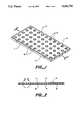
- FIG. 1is a perspective view of an overvoltage protection element in accordance with this invention
- FIG. 2is a view taken along the line 2--2 of FIG. 1;
- FIG. 3is an enlarged view taken along the line 3--3 of FIG. 2;
- FIG. 4shows the overvoltage protection element forming part of a device for multi-line overvoltage protection
- FIG. 5is a perspective view of an overvoltage protection element associated with a multiple line printed circuit board
- FIG. 6shows the overvoltage protection element in a connector arrangement
- FIG. 7shows the overvoltage protection device associated with another connector arrangement
- FIG. 8shows the overvoltage protection element associated with one of multiple conductors.
- the overvoltage protection elementincludes a sheet, layer or member 11, having spaced major surfaces which, as will be described, is selected to be of predetermined thickness.
- the sheetis formed of any electrically insulating material including, but not limited to, polymers including thermoplastic materials polyethylene, polypropylene, polyester, polymids, elastomers, natural and synthetic rubbers, silicon rubber, thermosetting materials, epoxies, ceramics or glass.
- the sheet 11is provided with a plurality of holes or openings 12 which extend from the bottom surface 13 to the top surface 14.
- the hole sizeshould be wider than about one-half the width of the associated electrical circuit.
- the hole shapemay be a circular cylinder, although holes of other shapes and sizes can be used.
- the shape and sizes of the holewill be, in part, dictated by methods of perforating the sheet of material. Holes having open areas of between 0.0003 and 0.20 square inches are suitable.
- the holescan be made by mechanical punching, laser processing and cutting, chemical etching, etc. Each of these and other methods of forming holes which extend through the sheet is dependent on the material used to form the sheet.
- the sheetis selected to have a predetermined thickness and the holes are filled with a suitable non-linear switching material of the type described in the patents referred to above, and preferably, a material such as taught in U.S. Pat. No. 4,977,357, comprising a binder and closely spaced conductive particles homogeneously distributed in said binder and spaced to provide electrical conduction by quantum mechanical tunneling.
- the materialextends between the two major surfaces.
- the holesmay be filled by a variety of methods including calendaring, pressing, laminating, molding, extruding, dipping, wiping, painting, rolling, etc. The only requirement is that the holes be completely filled so that the material extends coplanar with the upper and lower surfaces of the sheet.
- the size of the holesshould be such that for the particular application under consideration, there is a sufficient volume of material to carry the currents which are induced under an overvoltage condition.
- the overvoltage protection elementcan be formed in large sheets which can then be cut up for specific applications.
- the breakdown characteristic of the elementare controlled by the type of non-linear material used and the thickness of the sheet or member 11; that is, the spacing between the major surfaces. The greater the thickness, or spacing, the higher the voltage required to cause switching. Thicknesses between 0.001 and 0.10 inches are satisfactory.
- FIG. 4shows a piece cut from a sheet to form element 21.
- a conductive ground plane 22is affixed to the underside of the sheet in conductive contact with the non-linear material extending to the lower surface 23.
- a plurality of separate leads 24are applied to the upper surface 26 to be in intimate contact with the non-linear material extending to that surface. As shown, the dotted circles show the non-linear material in contact with the electrodes 24.
- the electrodes 24extend beyond the element and can be connected to electrical circuits.
- the bottom plate 22can be grounded whereby excessive voltage on any of the associated electrical leads 24 causes switching of the material between the corresponding electrode 24 and ground.
- the leads 24 and ground plane 22can be laminated to the element 21 by heat and pressure.
- conductive adhesivesmay be applied to the surfaces and the leads and member adhered to the surface in electrical contact with the non-linear material.
- the leads or traces 24may be formed by printed wiring techniques. That is, a sheet of conductive material may be applied and placed in intimate contact with the upper surface. Then by photolithographic techniques, selected regions of the conductive material are exposed whereby they may be etched away by acid or the like to leave traces 24.
- an element 31is placed on the surface of a printed circuit board 32 which includes electrical leads or traces 33.
- the upper surface of the element 31is covered with a conductive layer 34 which can be connected to ground, thereby switching excess voltage on any of the leads 33 to the ground plane through the nonlinear perforated overvoltage protection material.
- FIG. 6there is shown a printed circuit board 41 having conductive traces or leads 42 terminating in holes 43 for connection to associated electrical leads. Overlying the printed circuit conductors is an element 44 including the nonlinear material 46. A ground plane 47 is in conductive contact with the nonlinear material 46. In this manner, when overvoltages are applied to the leads associated with the holes 43, the non-linear material switches to connect the leads to the ground plane and divert excessive currents to ground plane 47.
- the conductors 51 associated with the lead holes 52are wrapped over the side of the insulating block 53 and cooperate with one surface 54 of the overvoltage protection element 56 with the other surface 57 connected to a ground plane 58.
- the insulating blockis supported in a metal shell 59.
- FIG. 8there is shown a sheet of overvoltage protection material 61.
- a conductive sheet 62is applied to one surface in intimate contact with the lead 63.
- the other surface of the overvoltage elementis provided with a conductive ground plane 64.
- an overvoltage protection elementformed from an impregnated fabric which is easy to manufacture and to control the electrical characteristics.
- the elementis adaptable for many applications for a multi-line circuit protection such as in connectors, printed circuit boards, and the like.
Landscapes
- Engineering & Computer Science (AREA)
- Microelectronics & Electronic Packaging (AREA)
- Physics & Mathematics (AREA)
- Electromagnetism (AREA)
- Emergency Protection Circuit Devices (AREA)
- Thermistors And Varistors (AREA)
Abstract
Description
Claims (8)
Priority Applications (1)
| Application Number | Priority Date | Filing Date | Title |
|---|---|---|---|
| US07/949,709US5262754A (en) | 1992-09-23 | 1992-09-23 | Overvoltage protection element |
Applications Claiming Priority (1)
| Application Number | Priority Date | Filing Date | Title |
|---|---|---|---|
| US07/949,709US5262754A (en) | 1992-09-23 | 1992-09-23 | Overvoltage protection element |
Publications (1)
| Publication Number | Publication Date |
|---|---|
| US5262754Atrue US5262754A (en) | 1993-11-16 |
Family
ID=25489457
Family Applications (1)
| Application Number | Title | Priority Date | Filing Date |
|---|---|---|---|
| US07/949,709Expired - LifetimeUS5262754A (en) | 1992-09-23 | 1992-09-23 | Overvoltage protection element |
Country Status (1)
| Country | Link |
|---|---|
| US (1) | US5262754A (en) |
Cited By (84)
| Publication number | Priority date | Publication date | Assignee | Title |
|---|---|---|---|---|
| US5393597A (en)* | 1992-09-23 | 1995-02-28 | The Whitaker Corporation | Overvoltage protection element |
| US5483407A (en)* | 1992-09-23 | 1996-01-09 | The Whitaker Corporation | Electrical overstress protection apparatus and method |
| US5537108A (en)* | 1994-02-08 | 1996-07-16 | Prolinx Labs Corporation | Method and structure for programming fuses |
| WO1996002922A3 (en)* | 1994-07-14 | 1996-07-25 | Oryx Techn Corp | Variable voltage protection structures and methods for making same |
| US5572409A (en)* | 1994-02-08 | 1996-11-05 | Prolinx Labs Corporation | Apparatus including a programmable socket adapter for coupling an electronic component to a component socket on a printed circuit board |
| WO1996041356A3 (en)* | 1995-06-07 | 1997-01-30 | Littelfuse Inc | Method and apparatus for a surface-mountable device for protection against electrostatic damage to electronic components |
| US5633620A (en)* | 1995-12-27 | 1997-05-27 | Microelectronic Modules Corporation | Arc containment system for lightning surge resistor networks |
| US5699032A (en)* | 1996-06-07 | 1997-12-16 | Littelfuse, Inc. | Surface-mount fuse having a substrate with surfaces and a metal strip attached to the substrate using layer of adhesive material |
| US5726482A (en) | 1994-02-08 | 1998-03-10 | Prolinx Labs Corporation | Device-under-test card for a burn-in board |
| US5767575A (en) | 1995-10-17 | 1998-06-16 | Prolinx Labs Corporation | Ball grid array structure and method for packaging an integrated circuit chip |
| US5790008A (en)* | 1994-05-27 | 1998-08-04 | Littlefuse, Inc. | Surface-mounted fuse device with conductive terminal pad layers and groove on side surfaces |
| US5808351A (en) | 1994-02-08 | 1998-09-15 | Prolinx Labs Corporation | Programmable/reprogramable structure using fuses and antifuses |
| US5807509A (en)* | 1994-07-14 | 1998-09-15 | Surgx Corporation | Single and multi layer variable voltage protection devices and method of making same |
| US5813881A (en) | 1994-02-08 | 1998-09-29 | Prolinx Labs Corporation | Programmable cable and cable adapter using fuses and antifuses |
| US5834824A (en) | 1994-02-08 | 1998-11-10 | Prolinx Labs Corporation | Use of conductive particles in a nonconductive body as an integrated circuit antifuse |
| US5844477A (en)* | 1994-05-27 | 1998-12-01 | Littelfuse, Inc. | Method of protecting a surface-mount fuse device |
| US5869869A (en)* | 1996-01-31 | 1999-02-09 | Lsi Logic Corporation | Microelectronic device with thin film electrostatic discharge protection structure |
| US5872338A (en) | 1996-04-10 | 1999-02-16 | Prolinx Labs Corporation | Multilayer board having insulating isolation rings |
| US5897388A (en)* | 1997-05-30 | 1999-04-27 | The Whitaker Corporation | Method of applying ESD protection to a shielded electrical |
| US5906043A (en) | 1995-01-18 | 1999-05-25 | Prolinx Labs Corporation | Programmable/reprogrammable structure using fuses and antifuses |
| US5906042A (en) | 1995-10-04 | 1999-05-25 | Prolinx Labs Corporation | Method and structure to interconnect traces of two conductive layers in a printed circuit board |
| US5917229A (en) | 1994-02-08 | 1999-06-29 | Prolinx Labs Corporation | Programmable/reprogrammable printed circuit board using fuse and/or antifuse as interconnect |
| US5928567A (en)* | 1995-10-31 | 1999-07-27 | The Whitaker Corporation | Overvoltage protection material |
| EP0879470A4 (en)* | 1996-01-22 | 1999-08-25 | Surgx Corp | Over-voltage protection device and method for making same |
| US5977860A (en)* | 1996-06-07 | 1999-11-02 | Littelfuse, Inc. | Surface-mount fuse and the manufacture thereof |
| US5974661A (en)* | 1994-05-27 | 1999-11-02 | Littelfuse, Inc. | Method of manufacturing a surface-mountable device for protection against electrostatic damage to electronic components |
| US6013358A (en)* | 1997-11-18 | 2000-01-11 | Cooper Industries, Inc. | Transient voltage protection device with ceramic substrate |
| US6034427A (en) | 1998-01-28 | 2000-03-07 | Prolinx Labs Corporation | Ball grid array structure and method for packaging an integrated circuit chip |
| US6064094A (en)* | 1998-03-10 | 2000-05-16 | Oryx Technology Corporation | Over-voltage protection system for integrated circuits using the bonding pads and passivation layer |
| US6172590B1 (en) | 1996-01-22 | 2001-01-09 | Surgx Corporation | Over-voltage protection device and method for making same |
| US6191928B1 (en) | 1994-05-27 | 2001-02-20 | Littelfuse, Inc. | Surface-mountable device for protection against electrostatic damage to electronic components |
| US6251513B1 (en) | 1997-11-08 | 2001-06-26 | Littlefuse, Inc. | Polymer composites for overvoltage protection |
| US6373719B1 (en) | 2000-04-13 | 2002-04-16 | Surgx Corporation | Over-voltage protection for electronic circuits |
| US20030013324A1 (en)* | 2001-07-10 | 2003-01-16 | Whitney Stephen J. | Connectors having circuit protection |
| US20030011026A1 (en)* | 2001-07-10 | 2003-01-16 | Colby James A. | Electrostatic discharge apparatus for network devices |
| US20030025587A1 (en)* | 2001-07-10 | 2003-02-06 | Whitney Stephen J. | Electrostatic discharge multifunction resistor |
| US20030062983A1 (en)* | 1999-11-19 | 2003-04-03 | Duggal Anil Raj | Current limiter device with an electrically conductive composite material and method of manufacturing |
| US6549114B2 (en) | 1998-08-20 | 2003-04-15 | Littelfuse, Inc. | Protection of electrical devices with voltage variable materials |
| US6560087B1 (en)* | 2000-09-01 | 2003-05-06 | Eagle Comtronics, Inc. | Electronic signal filter with surge protection mechanism |
| US20030122538A1 (en)* | 2000-09-28 | 2003-07-03 | Teradyne, Inc. | Coaxial cable for ATE with overvoltage protection |
| US6628498B2 (en) | 2000-08-28 | 2003-09-30 | Steven J. Whitney | Integrated electrostatic discharge and overcurrent device |
| US6642297B1 (en) | 1998-01-16 | 2003-11-04 | Littelfuse, Inc. | Polymer composite materials for electrostatic discharge protection |
| US20040119087A1 (en)* | 2002-08-28 | 2004-06-24 | Ixys Corporation | Breakdown voltage for power devices |
| US20060152334A1 (en)* | 2005-01-10 | 2006-07-13 | Nathaniel Maercklein | Electrostatic discharge protection for embedded components |
| US20060191713A1 (en)* | 2005-02-25 | 2006-08-31 | Chereson Jeffrey D | Fusible device and method |
| US7132922B2 (en) | 2002-04-08 | 2006-11-07 | Littelfuse, Inc. | Direct application voltage variable material, components thereof and devices employing same |
| US20060255379A1 (en)* | 2005-05-12 | 2006-11-16 | Ixys Corporation | Stable diodes for low and high frequency applications |
| US20070019346A1 (en)* | 2005-07-21 | 2007-01-25 | Kim Kyle Y | Transient voltage protection device, material, and manufacturing methods |
| US20070019354A1 (en)* | 2005-07-21 | 2007-01-25 | Kamath Hundi P | Transient voltage protection circuit boards and manufacturing methods |
| US7183891B2 (en) | 2002-04-08 | 2007-02-27 | Littelfuse, Inc. | Direct application voltage variable material, devices employing same and methods of manufacturing such devices |
| US7202770B2 (en) | 2002-04-08 | 2007-04-10 | Littelfuse, Inc. | Voltage variable material for direct application and devices employing same |
| US7258819B2 (en) | 2001-10-11 | 2007-08-21 | Littelfuse, Inc. | Voltage variable substrate material |
| US7285846B1 (en) | 2005-02-22 | 2007-10-23 | Littelfuse, Inc. | Integrated circuit package with ESD protection |
| CN100401610C (en)* | 2004-04-12 | 2008-07-09 | 四川中光高技术研究所有限责任公司 | Anti-explosion power source surge protector |
| US7446030B2 (en) | 1999-08-27 | 2008-11-04 | Shocking Technologies, Inc. | Methods for fabricating current-carrying structures using voltage switchable dielectric materials |
| US20090176410A1 (en)* | 2003-11-05 | 2009-07-09 | Christopher Alan Tutt | High frequency connector assembly |
| US20090251841A1 (en)* | 2008-04-04 | 2009-10-08 | Littelfuse, Inc. | Incorporating electrostatic protection into miniature connectors |
| US7695644B2 (en) | 1999-08-27 | 2010-04-13 | Shocking Technologies, Inc. | Device applications for voltage switchable dielectric material having high aspect ratio particles |
| US7793236B2 (en) | 2007-06-13 | 2010-09-07 | Shocking Technologies, Inc. | System and method for including protective voltage switchable dielectric material in the design or simulation of substrate devices |
| US7825491B2 (en) | 2005-11-22 | 2010-11-02 | Shocking Technologies, Inc. | Light-emitting device using voltage switchable dielectric material |
| US20100284115A1 (en)* | 2009-05-05 | 2010-11-11 | Interconnect Portfolio Llc | ESD Protection Utilizing Radiated Thermal Relief |
| US7872251B2 (en) | 2006-09-24 | 2011-01-18 | Shocking Technologies, Inc. | Formulations for voltage switchable dielectric material having a stepped voltage response and methods for making the same |
| US7923844B2 (en) | 2005-11-22 | 2011-04-12 | Shocking Technologies, Inc. | Semiconductor devices including voltage switchable materials for over-voltage protection |
| US7968015B2 (en) | 2006-07-29 | 2011-06-28 | Shocking Technologies, Inc. | Light-emitting diode device for voltage switchable dielectric material having high aspect ratio particles |
| US7983024B2 (en) | 2007-04-24 | 2011-07-19 | Littelfuse, Inc. | Fuse card system for automotive circuit protection |
| US8117743B2 (en) | 1999-08-27 | 2012-02-21 | Shocking Technologies, Inc. | Methods for fabricating current-carrying structures using voltage switchable dielectric materials |
| US8203421B2 (en) | 2008-04-14 | 2012-06-19 | Shocking Technologies, Inc. | Substrate device or package using embedded layer of voltage switchable dielectric material in a vertical switching configuration |
| US8206614B2 (en) | 2008-01-18 | 2012-06-26 | Shocking Technologies, Inc. | Voltage switchable dielectric material having bonded particle constituents |
| US8272123B2 (en) | 2009-01-27 | 2012-09-25 | Shocking Technologies, Inc. | Substrates having voltage switchable dielectric materials |
| US8362871B2 (en) | 2008-11-05 | 2013-01-29 | Shocking Technologies, Inc. | Geometric and electric field considerations for including transient protective material in substrate devices |
| US8399773B2 (en) | 2009-01-27 | 2013-03-19 | Shocking Technologies, Inc. | Substrates having voltage switchable dielectric materials |
| CN103155053A (en)* | 2010-10-05 | 2013-06-12 | 音羽电机工业株式会社 | Non-linear resistive element and manufacturing method thereof |
| JP2013219092A (en)* | 2012-04-04 | 2013-10-24 | Otowa Denki Kogyo Kk | Nonlinear resistor element |
| US20140125449A1 (en)* | 2012-04-04 | 2014-05-08 | Otowa Electric Co., Ltd. | Non-linear resistive element |
| US8968606B2 (en) | 2009-03-26 | 2015-03-03 | Littelfuse, Inc. | Components having voltage switchable dielectric materials |
| US9053844B2 (en) | 2009-09-09 | 2015-06-09 | Littelfuse, Inc. | Geometric configuration or alignment of protective material in a gap structure for electrical devices |
| US9082622B2 (en) | 2010-02-26 | 2015-07-14 | Littelfuse, Inc. | Circuit elements comprising ferroic materials |
| US9208930B2 (en) | 2008-09-30 | 2015-12-08 | Littelfuse, Inc. | Voltage switchable dielectric material containing conductive core shelled particles |
| US9208931B2 (en) | 2008-09-30 | 2015-12-08 | Littelfuse, Inc. | Voltage switchable dielectric material containing conductor-on-conductor core shelled particles |
| US9226391B2 (en) | 2009-01-27 | 2015-12-29 | Littelfuse, Inc. | Substrates having voltage switchable dielectric materials |
| US9224728B2 (en) | 2010-02-26 | 2015-12-29 | Littelfuse, Inc. | Embedded protection against spurious electrical events |
| US9320135B2 (en) | 2010-02-26 | 2016-04-19 | Littelfuse, Inc. | Electric discharge protection for surface mounted and embedded components |
| US20200168372A1 (en)* | 2018-11-27 | 2020-05-28 | Samsung Electro-Mechanics Co., Ltd. | Varistor and method of manufacturing the same |
| US10892072B1 (en)* | 2019-08-15 | 2021-01-12 | Polytronics Technology Corp. | PTC device |
Citations (6)
| Publication number | Priority date | Publication date | Assignee | Title |
|---|---|---|---|---|
| US1452574A (en)* | 1918-06-29 | 1923-04-24 | Westinghouse Electric & Mfg Co | Circuit interrupter |
| US2707223A (en)* | 1949-06-15 | 1955-04-26 | Hans E Hollmann | Electric resistor |
| US3212043A (en)* | 1961-04-11 | 1965-10-12 | Ass Elect Ind | Low voltage non-linear electrical resistance elements and method of manufacture thereof |
| US3685026A (en)* | 1970-08-20 | 1972-08-15 | Matsushita Electric Industrial Co Ltd | Process of switching an electric current |
| US4726991A (en)* | 1986-07-10 | 1988-02-23 | Eos Technologies Inc. | Electrical overstress protection material and process |
| US4977357A (en)* | 1988-01-11 | 1990-12-11 | Shrier Karen P | Overvoltage protection device and material |
- 1992
- 1992-09-23USUS07/949,709patent/US5262754A/ennot_activeExpired - Lifetime
Patent Citations (6)
| Publication number | Priority date | Publication date | Assignee | Title |
|---|---|---|---|---|
| US1452574A (en)* | 1918-06-29 | 1923-04-24 | Westinghouse Electric & Mfg Co | Circuit interrupter |
| US2707223A (en)* | 1949-06-15 | 1955-04-26 | Hans E Hollmann | Electric resistor |
| US3212043A (en)* | 1961-04-11 | 1965-10-12 | Ass Elect Ind | Low voltage non-linear electrical resistance elements and method of manufacture thereof |
| US3685026A (en)* | 1970-08-20 | 1972-08-15 | Matsushita Electric Industrial Co Ltd | Process of switching an electric current |
| US4726991A (en)* | 1986-07-10 | 1988-02-23 | Eos Technologies Inc. | Electrical overstress protection material and process |
| US4977357A (en)* | 1988-01-11 | 1990-12-11 | Shrier Karen P | Overvoltage protection device and material |
Cited By (139)
| Publication number | Priority date | Publication date | Assignee | Title |
|---|---|---|---|---|
| US5483407A (en)* | 1992-09-23 | 1996-01-09 | The Whitaker Corporation | Electrical overstress protection apparatus and method |
| US5393597A (en)* | 1992-09-23 | 1995-02-28 | The Whitaker Corporation | Overvoltage protection element |
| US5917229A (en) | 1994-02-08 | 1999-06-29 | Prolinx Labs Corporation | Programmable/reprogrammable printed circuit board using fuse and/or antifuse as interconnect |
| US5537108A (en)* | 1994-02-08 | 1996-07-16 | Prolinx Labs Corporation | Method and structure for programming fuses |
| US5834824A (en) | 1994-02-08 | 1998-11-10 | Prolinx Labs Corporation | Use of conductive particles in a nonconductive body as an integrated circuit antifuse |
| US5572409A (en)* | 1994-02-08 | 1996-11-05 | Prolinx Labs Corporation | Apparatus including a programmable socket adapter for coupling an electronic component to a component socket on a printed circuit board |
| US5813881A (en) | 1994-02-08 | 1998-09-29 | Prolinx Labs Corporation | Programmable cable and cable adapter using fuses and antifuses |
| US5808351A (en) | 1994-02-08 | 1998-09-15 | Prolinx Labs Corporation | Programmable/reprogramable structure using fuses and antifuses |
| US5726482A (en) | 1994-02-08 | 1998-03-10 | Prolinx Labs Corporation | Device-under-test card for a burn-in board |
| US5790008A (en)* | 1994-05-27 | 1998-08-04 | Littlefuse, Inc. | Surface-mounted fuse device with conductive terminal pad layers and groove on side surfaces |
| US5844477A (en)* | 1994-05-27 | 1998-12-01 | Littelfuse, Inc. | Method of protecting a surface-mount fuse device |
| US6191928B1 (en) | 1994-05-27 | 2001-02-20 | Littelfuse, Inc. | Surface-mountable device for protection against electrostatic damage to electronic components |
| US6023028A (en)* | 1994-05-27 | 2000-02-08 | Littelfuse, Inc. | Surface-mountable device having a voltage variable polgmeric material for protection against electrostatic damage to electronic components |
| US5974661A (en)* | 1994-05-27 | 1999-11-02 | Littelfuse, Inc. | Method of manufacturing a surface-mountable device for protection against electrostatic damage to electronic components |
| US5943764A (en)* | 1994-05-27 | 1999-08-31 | Littelfuse, Inc. | Method of manufacturing a surface-mounted fuse device |
| US6310752B1 (en) | 1994-07-14 | 2001-10-30 | Surgx Corporation | Variable voltage protection structures and method for making same |
| CN1079571C (en)* | 1994-07-14 | 2002-02-20 | 苏吉克斯公司 | Variable voltage protection structures and methods for making same |
| US5807509A (en)* | 1994-07-14 | 1998-09-15 | Surgx Corporation | Single and multi layer variable voltage protection devices and method of making same |
| US6542065B2 (en)* | 1994-07-14 | 2003-04-01 | Surgx Corporation | Variable voltage protection structures and method for making same |
| WO1996002922A3 (en)* | 1994-07-14 | 1996-07-25 | Oryx Techn Corp | Variable voltage protection structures and methods for making same |
| US6239687B1 (en)* | 1994-07-14 | 2001-05-29 | Surgx Corporation | Variable voltage protection structures and method for making same |
| AU704862B2 (en)* | 1994-07-14 | 1999-05-06 | Surgx Corporation | Variable voltage protection structures and methods for making same |
| US5906043A (en) | 1995-01-18 | 1999-05-25 | Prolinx Labs Corporation | Programmable/reprogrammable structure using fuses and antifuses |
| US5962815A (en) | 1995-01-18 | 1999-10-05 | Prolinx Labs Corporation | Antifuse interconnect between two conducting layers of a printed circuit board |
| WO1996041356A3 (en)* | 1995-06-07 | 1997-01-30 | Littelfuse Inc | Method and apparatus for a surface-mountable device for protection against electrostatic damage to electronic components |
| US5906042A (en) | 1995-10-04 | 1999-05-25 | Prolinx Labs Corporation | Method and structure to interconnect traces of two conductive layers in a printed circuit board |
| US5767575A (en) | 1995-10-17 | 1998-06-16 | Prolinx Labs Corporation | Ball grid array structure and method for packaging an integrated circuit chip |
| US5928567A (en)* | 1995-10-31 | 1999-07-27 | The Whitaker Corporation | Overvoltage protection material |
| US5633620A (en)* | 1995-12-27 | 1997-05-27 | Microelectronic Modules Corporation | Arc containment system for lightning surge resistor networks |
| US6172590B1 (en) | 1996-01-22 | 2001-01-09 | Surgx Corporation | Over-voltage protection device and method for making same |
| EP0879470A4 (en)* | 1996-01-22 | 1999-08-25 | Surgx Corp | Over-voltage protection device and method for making same |
| US5869869A (en)* | 1996-01-31 | 1999-02-09 | Lsi Logic Corporation | Microelectronic device with thin film electrostatic discharge protection structure |
| US5955762A (en)* | 1996-01-31 | 1999-09-21 | Lsi Logic Corporation | Microelectronic package with polymer ESD protection |
| US5970321A (en)* | 1996-01-31 | 1999-10-19 | Lsi Logic Corporation | Method of fabricating a microelectronic package having polymer ESD protection |
| US5987744A (en) | 1996-04-10 | 1999-11-23 | Prolinx Labs Corporation | Method for supporting one or more electronic components |
| US5872338A (en) | 1996-04-10 | 1999-02-16 | Prolinx Labs Corporation | Multilayer board having insulating isolation rings |
| US5699032A (en)* | 1996-06-07 | 1997-12-16 | Littelfuse, Inc. | Surface-mount fuse having a substrate with surfaces and a metal strip attached to the substrate using layer of adhesive material |
| US5977860A (en)* | 1996-06-07 | 1999-11-02 | Littelfuse, Inc. | Surface-mount fuse and the manufacture thereof |
| US5897388A (en)* | 1997-05-30 | 1999-04-27 | The Whitaker Corporation | Method of applying ESD protection to a shielded electrical |
| US6251513B1 (en) | 1997-11-08 | 2001-06-26 | Littlefuse, Inc. | Polymer composites for overvoltage protection |
| US6013358A (en)* | 1997-11-18 | 2000-01-11 | Cooper Industries, Inc. | Transient voltage protection device with ceramic substrate |
| US6642297B1 (en) | 1998-01-16 | 2003-11-04 | Littelfuse, Inc. | Polymer composite materials for electrostatic discharge protection |
| US6034427A (en) | 1998-01-28 | 2000-03-07 | Prolinx Labs Corporation | Ball grid array structure and method for packaging an integrated circuit chip |
| US6064094A (en)* | 1998-03-10 | 2000-05-16 | Oryx Technology Corporation | Over-voltage protection system for integrated circuits using the bonding pads and passivation layer |
| US6693508B2 (en) | 1998-08-20 | 2004-02-17 | Littelfuse, Inc. | Protection of electrical devices with voltage variable materials |
| US6549114B2 (en) | 1998-08-20 | 2003-04-15 | Littelfuse, Inc. | Protection of electrical devices with voltage variable materials |
| US7695644B2 (en) | 1999-08-27 | 2010-04-13 | Shocking Technologies, Inc. | Device applications for voltage switchable dielectric material having high aspect ratio particles |
| US9144151B2 (en) | 1999-08-27 | 2015-09-22 | Littelfuse, Inc. | Current-carrying structures fabricated using voltage switchable dielectric materials |
| US8117743B2 (en) | 1999-08-27 | 2012-02-21 | Shocking Technologies, Inc. | Methods for fabricating current-carrying structures using voltage switchable dielectric materials |
| US7446030B2 (en) | 1999-08-27 | 2008-11-04 | Shocking Technologies, Inc. | Methods for fabricating current-carrying structures using voltage switchable dielectric materials |
| US20030062983A1 (en)* | 1999-11-19 | 2003-04-03 | Duggal Anil Raj | Current limiter device with an electrically conductive composite material and method of manufacturing |
| US6711807B2 (en)* | 1999-11-19 | 2004-03-30 | General Electric Company | Method of manufacturing composite array structure |
| US6570765B2 (en) | 2000-04-13 | 2003-05-27 | Gerald R. Behling | Over-voltage protection for electronic circuits |
| US6373719B1 (en) | 2000-04-13 | 2002-04-16 | Surgx Corporation | Over-voltage protection for electronic circuits |
| US6628498B2 (en) | 2000-08-28 | 2003-09-30 | Steven J. Whitney | Integrated electrostatic discharge and overcurrent device |
| US6560087B1 (en)* | 2000-09-01 | 2003-05-06 | Eagle Comtronics, Inc. | Electronic signal filter with surge protection mechanism |
| US6939175B2 (en)* | 2000-09-28 | 2005-09-06 | Teradyne, Inc. | Coaxial cable for overvoltage protection |
| US20030122538A1 (en)* | 2000-09-28 | 2003-07-03 | Teradyne, Inc. | Coaxial cable for ATE with overvoltage protection |
| WO2003007452A1 (en)* | 2001-07-10 | 2003-01-23 | Littelfuse, Inc. | Electrostatic discharge apparatus for network devices |
| US7035072B2 (en) | 2001-07-10 | 2006-04-25 | Littlefuse, Inc. | Electrostatic discharge apparatus for network devices |
| US7034652B2 (en) | 2001-07-10 | 2006-04-25 | Littlefuse, Inc. | Electrostatic discharge multifunction resistor |
| US6935879B2 (en)* | 2001-07-10 | 2005-08-30 | Littelfuse, Inc. | Connectors having circuit protection |
| US20030025587A1 (en)* | 2001-07-10 | 2003-02-06 | Whitney Stephen J. | Electrostatic discharge multifunction resistor |
| US20030011026A1 (en)* | 2001-07-10 | 2003-01-16 | Colby James A. | Electrostatic discharge apparatus for network devices |
| US20030013324A1 (en)* | 2001-07-10 | 2003-01-16 | Whitney Stephen J. | Connectors having circuit protection |
| US7258819B2 (en) | 2001-10-11 | 2007-08-21 | Littelfuse, Inc. | Voltage variable substrate material |
| US7609141B2 (en) | 2002-04-08 | 2009-10-27 | Littelfuse, Inc. | Flexible circuit having overvoltage protection |
| US7843308B2 (en) | 2002-04-08 | 2010-11-30 | Littlefuse, Inc. | Direct application voltage variable material |
| US7132922B2 (en) | 2002-04-08 | 2006-11-07 | Littelfuse, Inc. | Direct application voltage variable material, components thereof and devices employing same |
| US7183891B2 (en) | 2002-04-08 | 2007-02-27 | Littelfuse, Inc. | Direct application voltage variable material, devices employing same and methods of manufacturing such devices |
| US7202770B2 (en) | 2002-04-08 | 2007-04-10 | Littelfuse, Inc. | Voltage variable material for direct application and devices employing same |
| US8093652B2 (en)* | 2002-08-28 | 2012-01-10 | Ixys Corporation | Breakdown voltage for power devices |
| US20040119087A1 (en)* | 2002-08-28 | 2004-06-24 | Ixys Corporation | Breakdown voltage for power devices |
| US20090176410A1 (en)* | 2003-11-05 | 2009-07-09 | Christopher Alan Tutt | High frequency connector assembly |
| US7997907B2 (en) | 2003-11-05 | 2011-08-16 | Tensolite, Llc | High frequency connector assembly |
| US20100273350A1 (en)* | 2003-11-05 | 2010-10-28 | Christopher Alan Tutt | High frequency connector assembly |
| US7748990B2 (en) | 2003-11-05 | 2010-07-06 | Tensolite, Llc | High frequency connector assembly |
| CN100401610C (en)* | 2004-04-12 | 2008-07-09 | 四川中光高技术研究所有限责任公司 | Anti-explosion power source surge protector |
| US20060152334A1 (en)* | 2005-01-10 | 2006-07-13 | Nathaniel Maercklein | Electrostatic discharge protection for embedded components |
| US7285846B1 (en) | 2005-02-22 | 2007-10-23 | Littelfuse, Inc. | Integrated circuit package with ESD protection |
| US20060191713A1 (en)* | 2005-02-25 | 2006-08-31 | Chereson Jeffrey D | Fusible device and method |
| US8716745B2 (en) | 2005-05-12 | 2014-05-06 | Ixys Corporation | Stable diodes for low and high frequency applications |
| US20060255379A1 (en)* | 2005-05-12 | 2006-11-16 | Ixys Corporation | Stable diodes for low and high frequency applications |
| US20070019354A1 (en)* | 2005-07-21 | 2007-01-25 | Kamath Hundi P | Transient voltage protection circuit boards and manufacturing methods |
| US7567416B2 (en) | 2005-07-21 | 2009-07-28 | Cooper Technologies Company | Transient voltage protection device, material, and manufacturing methods |
| US20070019346A1 (en)* | 2005-07-21 | 2007-01-25 | Kim Kyle Y | Transient voltage protection device, material, and manufacturing methods |
| US7612976B2 (en) | 2005-07-21 | 2009-11-03 | Cooper Technologies Company | Transient voltage protection circuit boards and manufacturing methods |
| JP2007037397A (en)* | 2005-07-21 | 2007-02-08 | Cooper Technol Co | Transient voltage suppression device, transient voltage suppression chip device, manufacturing method of transient voltage suppression device, impedance material, and manufacturing method of impedance material |
| US20090257166A1 (en)* | 2005-07-21 | 2009-10-15 | Cooper Technologies Company | Transient Voltage Protection Device, Material, and Manufacturing Methods |
| US8310799B2 (en) | 2005-07-21 | 2012-11-13 | Cooper Technologies Company | Transient voltage protection device, material, and manufacturing methods |
| US7825491B2 (en) | 2005-11-22 | 2010-11-02 | Shocking Technologies, Inc. | Light-emitting device using voltage switchable dielectric material |
| US8310064B2 (en) | 2005-11-22 | 2012-11-13 | Shocking Technologies, Inc. | Semiconductor devices including voltage switchable materials for over-voltage protection |
| US7923844B2 (en) | 2005-11-22 | 2011-04-12 | Shocking Technologies, Inc. | Semiconductor devices including voltage switchable materials for over-voltage protection |
| US7981325B2 (en) | 2006-07-29 | 2011-07-19 | Shocking Technologies, Inc. | Electronic device for voltage switchable dielectric material having high aspect ratio particles |
| US7968014B2 (en) | 2006-07-29 | 2011-06-28 | Shocking Technologies, Inc. | Device applications for voltage switchable dielectric material having high aspect ratio particles |
| US7968010B2 (en) | 2006-07-29 | 2011-06-28 | Shocking Technologies, Inc. | Method for electroplating a substrate |
| US7968015B2 (en) | 2006-07-29 | 2011-06-28 | Shocking Technologies, Inc. | Light-emitting diode device for voltage switchable dielectric material having high aspect ratio particles |
| GB2440662A (en)* | 2006-08-03 | 2008-02-06 | Cooper Technologies Co | Transient voltage protection circuit boards and manufacturing methods |
| GB2440662B (en)* | 2006-08-03 | 2011-05-04 | Cooper Technologies Co | Transient voltage protection circuit boards and manufacturing methods |
| CN101226798B (en)* | 2006-08-03 | 2012-06-27 | 库帕技术公司 | Transient voltage protection circuit boards and manufacturing method |
| US7872251B2 (en) | 2006-09-24 | 2011-01-18 | Shocking Technologies, Inc. | Formulations for voltage switchable dielectric material having a stepped voltage response and methods for making the same |
| US8163595B2 (en) | 2006-09-24 | 2012-04-24 | Shocking Technologies, Inc. | Formulations for voltage switchable dielectric materials having a stepped voltage response and methods for making the same |
| US7983024B2 (en) | 2007-04-24 | 2011-07-19 | Littelfuse, Inc. | Fuse card system for automotive circuit protection |
| US7793236B2 (en) | 2007-06-13 | 2010-09-07 | Shocking Technologies, Inc. | System and method for including protective voltage switchable dielectric material in the design or simulation of substrate devices |
| US8206614B2 (en) | 2008-01-18 | 2012-06-26 | Shocking Technologies, Inc. | Voltage switchable dielectric material having bonded particle constituents |
| US7952848B2 (en) | 2008-04-04 | 2011-05-31 | Littelfuse, Inc. | Incorporating electrostatic protection into miniature connectors |
| DE102009015962A1 (en) | 2008-04-04 | 2009-11-05 | Littlefuse, Inc., Des Plaines | Insertion of electrostatic protection in miniature connectors |
| US20090251841A1 (en)* | 2008-04-04 | 2009-10-08 | Littelfuse, Inc. | Incorporating electrostatic protection into miniature connectors |
| US8203421B2 (en) | 2008-04-14 | 2012-06-19 | Shocking Technologies, Inc. | Substrate device or package using embedded layer of voltage switchable dielectric material in a vertical switching configuration |
| US9208930B2 (en) | 2008-09-30 | 2015-12-08 | Littelfuse, Inc. | Voltage switchable dielectric material containing conductive core shelled particles |
| US9208931B2 (en) | 2008-09-30 | 2015-12-08 | Littelfuse, Inc. | Voltage switchable dielectric material containing conductor-on-conductor core shelled particles |
| US8362871B2 (en) | 2008-11-05 | 2013-01-29 | Shocking Technologies, Inc. | Geometric and electric field considerations for including transient protective material in substrate devices |
| US8399773B2 (en) | 2009-01-27 | 2013-03-19 | Shocking Technologies, Inc. | Substrates having voltage switchable dielectric materials |
| US9226391B2 (en) | 2009-01-27 | 2015-12-29 | Littelfuse, Inc. | Substrates having voltage switchable dielectric materials |
| US8272123B2 (en) | 2009-01-27 | 2012-09-25 | Shocking Technologies, Inc. | Substrates having voltage switchable dielectric materials |
| US8968606B2 (en) | 2009-03-26 | 2015-03-03 | Littelfuse, Inc. | Components having voltage switchable dielectric materials |
| KR20120038404A (en)* | 2009-05-05 | 2012-04-23 | 삼성전자주식회사 | Esd protection utilizing radiated thermal relief |
| US8199450B2 (en)* | 2009-05-05 | 2012-06-12 | Samsung Electronics Co., Ltd. | ESD protection utilizing radiated thermal relief |
| US20100284115A1 (en)* | 2009-05-05 | 2010-11-11 | Interconnect Portfolio Llc | ESD Protection Utilizing Radiated Thermal Relief |
| US9053844B2 (en) | 2009-09-09 | 2015-06-09 | Littelfuse, Inc. | Geometric configuration or alignment of protective material in a gap structure for electrical devices |
| US9082622B2 (en) | 2010-02-26 | 2015-07-14 | Littelfuse, Inc. | Circuit elements comprising ferroic materials |
| US9320135B2 (en) | 2010-02-26 | 2016-04-19 | Littelfuse, Inc. | Electric discharge protection for surface mounted and embedded components |
| US9224728B2 (en) | 2010-02-26 | 2015-12-29 | Littelfuse, Inc. | Embedded protection against spurious electrical events |
| KR20140012014A (en)* | 2010-10-05 | 2014-01-29 | 오토와덴키고교 가부시키가이샤 | Non-linear resistive element and manufacturing method thereof |
| US8896409B2 (en)* | 2010-10-05 | 2014-11-25 | Otowa Electric Co., Ltd. | Non-linear resistive element and manufacturing method thereof |
| CN103155053B (en)* | 2010-10-05 | 2016-04-20 | 音羽电机工业株式会社 | Nonlinear resistive element and manufacture method thereof |
| CN103155053A (en)* | 2010-10-05 | 2013-06-12 | 音羽电机工业株式会社 | Non-linear resistive element and manufacturing method thereof |
| US20130169405A1 (en)* | 2010-10-05 | 2013-07-04 | Otowa Electric Co., Ltd. | Non-linear resistive element and manufacturing method thereof |
| US9007167B2 (en)* | 2012-04-04 | 2015-04-14 | Otowa Electric Co., Ltd. | Non-linear resistive element |
| JP2013219092A (en)* | 2012-04-04 | 2013-10-24 | Otowa Denki Kogyo Kk | Nonlinear resistor element |
| CN103563014A (en)* | 2012-04-04 | 2014-02-05 | 音羽电机工业株式会社 | Nonlinear resistive element |
| US20140085043A1 (en)* | 2012-04-04 | 2014-03-27 | Otowa Electric Co., Ltd | Non-linear resistive element |
| EP2704158A4 (en)* | 2012-04-04 | 2014-10-22 | Otowa Electric Co Ltd | NON-LINEAR RESISTIVE ELEMENT |
| US20140125449A1 (en)* | 2012-04-04 | 2014-05-08 | Otowa Electric Co., Ltd. | Non-linear resistive element |
| US8902039B2 (en)* | 2012-04-04 | 2014-12-02 | Otowa Electric Co., Ltd. | Non-linear resistive element |
| CN103563014B (en)* | 2012-04-04 | 2017-09-01 | 音羽电机工业株式会社 | Nonlinear resistive element |
| US20200168372A1 (en)* | 2018-11-27 | 2020-05-28 | Samsung Electro-Mechanics Co., Ltd. | Varistor and method of manufacturing the same |
| US10839994B2 (en)* | 2018-11-27 | 2020-11-17 | Samsung Electro-Mechanics Co., Ltd. | Varistor and method of manufacturing the same |
| US10892072B1 (en)* | 2019-08-15 | 2021-01-12 | Polytronics Technology Corp. | PTC device |
Similar Documents
| Publication | Publication Date | Title |
|---|---|---|
| US5262754A (en) | Overvoltage protection element | |
| US5393597A (en) | Overvoltage protection element | |
| AU704862B2 (en) | Variable voltage protection structures and methods for making same | |
| US5278535A (en) | Electrical overstress pulse protection | |
| US5483407A (en) | Electrical overstress protection apparatus and method | |
| US5183698A (en) | Electrical overstress pulse protection | |
| US7417194B2 (en) | ESD protection devices and methods of making same using standard manufacturing processes | |
| US5340641A (en) | Electrical overstress pulse protection | |
| US4287394A (en) | Keyboard switch assembly with printed circuit board | |
| US20060152334A1 (en) | Electrostatic discharge protection for embedded components | |
| US5061830A (en) | Extension electrical switch system and method of manufacture | |
| US6282072B1 (en) | Electrical devices having a polymer PTC array | |
| KR970061017A (en) | Anisotropic conductive sheet with conductor layer and wiring board using the same | |
| TW359862B (en) | PTC conductive polymer protection device for surface mounting on a printed circuit board | |
| KR930019083A (en) | Heat-sealable interface plates | |
| US4651123A (en) | Linear potentiometer | |
| CA2045529A1 (en) | Flexible heating element | |
| EP1102338A4 (en) | Ptc element, ptc element-mounted pcb board, secondary cell protection circuit device and secondary cell assembly | |
| AU2003224689A1 (en) | Conductive polymer device and method of manufacturing same | |
| KR920007747B1 (en) | Sheet switch | |
| GB2077508A (en) | Variable resistance pressure- sensitive laminate | |
| US4694126A (en) | Membrane keyboard switch assembly having spacer structure and method of making | |
| EP0591348B1 (en) | Circuit protection devices | |
| US4012710A (en) | Multiple output potentiometer network | |
| DE3586994D1 (en) | ELECTRICAL CONTACT BETWEEN METALS AND RESISTANCE ELEMENTS. |
Legal Events
| Date | Code | Title | Description |
|---|---|---|---|
| AS | Assignment | Owner name:ELECTROMER CORPORATION, CALIFORNIA Free format text:ASSIGNMENT OF ASSIGNORS INTEREST.;ASSIGNOR:COLLINS, CHRISTOPHER J.;REEL/FRAME:006376/0830 Effective date:19920826 | |
| STCF | Information on status: patent grant | Free format text:PATENTED CASE | |
| AS | Assignment | Owner name:WHITAKER CORPORATION, THE, DELAWARE Free format text:ASSIGNMENT OF ASSIGNORS INTEREST;ASSIGNOR:ELECTROMER CORPORATION;REEL/FRAME:007188/0882 Effective date:19940902 | |
| FPAY | Fee payment | Year of fee payment:4 | |
| FEPP | Fee payment procedure | Free format text:PAYOR NUMBER ASSIGNED (ORIGINAL EVENT CODE: ASPN); ENTITY STATUS OF PATENT OWNER: LARGE ENTITY | |
| FPAY | Fee payment | Year of fee payment:8 | |
| FPAY | Fee payment | Year of fee payment:12 | |
| AS | Assignment | Owner name:THE WHITAKER LLC, DELAWARE Free format text:CONVERSION FROM CORPORATION TO LLC;ASSIGNOR:THE WHITAKER CORPORATION;REEL/FRAME:038040/0839 Effective date:20100924 | |
| AS | Assignment | Owner name:LITTELFUSE, INC., ILLINOIS Free format text:ASSIGNMENT OF ASSIGNORS INTEREST;ASSIGNOR:THE WHITAKER LLC;REEL/FRAME:039213/0451 Effective date:20160325 |