US5261593A - Direct application of unpackaged integrated circuit to flexible printed circuit - Google Patents
Direct application of unpackaged integrated circuit to flexible printed circuitDownload PDFInfo
- Publication number
- US5261593A US5261593AUS07/932,064US93206492AUS5261593AUS 5261593 AUS5261593 AUS 5261593AUS 93206492 AUS93206492 AUS 93206492AUS 5261593 AUS5261593 AUS 5261593A
- Authority
- US
- United States
- Prior art keywords
- solder
- substrate
- assembly
- solder paste
- chips
- Prior art date
- Legal status (The legal status is an assumption and is not a legal conclusion. Google has not performed a legal analysis and makes no representation as to the accuracy of the status listed.)
- Expired - Lifetime
Links
Images


Classifications
- H—ELECTRICITY
- H01—ELECTRIC ELEMENTS
- H01L—SEMICONDUCTOR DEVICES NOT COVERED BY CLASS H10
- H01L24/00—Arrangements for connecting or disconnecting semiconductor or solid-state bodies; Methods or apparatus related thereto
- H01L24/80—Methods for connecting semiconductor or other solid state bodies using means for bonding being attached to, or being formed on, the surface to be connected
- H01L24/81—Methods for connecting semiconductor or other solid state bodies using means for bonding being attached to, or being formed on, the surface to be connected using a bump connector
- H—ELECTRICITY
- H01—ELECTRIC ELEMENTS
- H01L—SEMICONDUCTOR DEVICES NOT COVERED BY CLASS H10
- H01L23/00—Details of semiconductor or other solid state devices
- H01L23/48—Arrangements for conducting electric current to or from the solid state body in operation, e.g. leads, terminal arrangements ; Selection of materials therefor
- H01L23/488—Arrangements for conducting electric current to or from the solid state body in operation, e.g. leads, terminal arrangements ; Selection of materials therefor consisting of soldered or bonded constructions
- H01L23/498—Leads, i.e. metallisations or lead-frames on insulating substrates, e.g. chip carriers
- H01L23/4985—Flexible insulating substrates
- H—ELECTRICITY
- H05—ELECTRIC TECHNIQUES NOT OTHERWISE PROVIDED FOR
- H05K—PRINTED CIRCUITS; CASINGS OR CONSTRUCTIONAL DETAILS OF ELECTRIC APPARATUS; MANUFACTURE OF ASSEMBLAGES OF ELECTRICAL COMPONENTS
- H05K3/00—Apparatus or processes for manufacturing printed circuits
- H05K3/30—Assembling printed circuits with electric components, e.g. with resistor
- H05K3/32—Assembling printed circuits with electric components, e.g. with resistor electrically connecting electric components or wires to printed circuits
- H05K3/34—Assembling printed circuits with electric components, e.g. with resistor electrically connecting electric components or wires to printed circuits by soldering
- H05K3/341—Surface mounted components
- H05K3/3431—Leadless components
- H05K3/3436—Leadless components having an array of bottom contacts, e.g. pad grid array or ball grid array components
- H—ELECTRICITY
- H01—ELECTRIC ELEMENTS
- H01L—SEMICONDUCTOR DEVICES NOT COVERED BY CLASS H10
- H01L2223/00—Details relating to semiconductor or other solid state devices covered by the group H01L23/00
- H01L2223/544—Marks applied to semiconductor devices or parts
- H01L2223/54473—Marks applied to semiconductor devices or parts for use after dicing
- H01L2223/5448—Located on chip prior to dicing and remaining on chip after dicing
- H—ELECTRICITY
- H01—ELECTRIC ELEMENTS
- H01L—SEMICONDUCTOR DEVICES NOT COVERED BY CLASS H10
- H01L2224/00—Indexing scheme for arrangements for connecting or disconnecting semiconductor or solid-state bodies and methods related thereto as covered by H01L24/00
- H01L2224/01—Means for bonding being attached to, or being formed on, the surface to be connected, e.g. chip-to-package, die-attach, "first-level" interconnects; Manufacturing methods related thereto
- H01L2224/02—Bonding areas; Manufacturing methods related thereto
- H01L2224/04—Structure, shape, material or disposition of the bonding areas prior to the connecting process
- H01L2224/0401—Bonding areas specifically adapted for bump connectors, e.g. under bump metallisation [UBM]
- H—ELECTRICITY
- H01—ELECTRIC ELEMENTS
- H01L—SEMICONDUCTOR DEVICES NOT COVERED BY CLASS H10
- H01L2224/00—Indexing scheme for arrangements for connecting or disconnecting semiconductor or solid-state bodies and methods related thereto as covered by H01L24/00
- H01L2224/01—Means for bonding being attached to, or being formed on, the surface to be connected, e.g. chip-to-package, die-attach, "first-level" interconnects; Manufacturing methods related thereto
- H01L2224/02—Bonding areas; Manufacturing methods related thereto
- H01L2224/04—Structure, shape, material or disposition of the bonding areas prior to the connecting process
- H01L2224/05—Structure, shape, material or disposition of the bonding areas prior to the connecting process of an individual bonding area
- H01L2224/0554—External layer
- H01L2224/0556—Disposition
- H01L2224/05571—Disposition the external layer being disposed in a recess of the surface
- H01L2224/05572—Disposition the external layer being disposed in a recess of the surface the external layer extending out of an opening
- H—ELECTRICITY
- H01—ELECTRIC ELEMENTS
- H01L—SEMICONDUCTOR DEVICES NOT COVERED BY CLASS H10
- H01L2224/00—Indexing scheme for arrangements for connecting or disconnecting semiconductor or solid-state bodies and methods related thereto as covered by H01L24/00
- H01L2224/01—Means for bonding being attached to, or being formed on, the surface to be connected, e.g. chip-to-package, die-attach, "first-level" interconnects; Manufacturing methods related thereto
- H01L2224/10—Bump connectors; Manufacturing methods related thereto
- H01L2224/12—Structure, shape, material or disposition of the bump connectors prior to the connecting process
- H01L2224/13—Structure, shape, material or disposition of the bump connectors prior to the connecting process of an individual bump connector
- H01L2224/13001—Core members of the bump connector
- H01L2224/13005—Structure
- H01L2224/13007—Bump connector smaller than the underlying bonding area, e.g. than the under bump metallisation [UBM]
- H—ELECTRICITY
- H01—ELECTRIC ELEMENTS
- H01L—SEMICONDUCTOR DEVICES NOT COVERED BY CLASS H10
- H01L2224/00—Indexing scheme for arrangements for connecting or disconnecting semiconductor or solid-state bodies and methods related thereto as covered by H01L24/00
- H01L2224/01—Means for bonding being attached to, or being formed on, the surface to be connected, e.g. chip-to-package, die-attach, "first-level" interconnects; Manufacturing methods related thereto
- H01L2224/10—Bump connectors; Manufacturing methods related thereto
- H01L2224/12—Structure, shape, material or disposition of the bump connectors prior to the connecting process
- H01L2224/13—Structure, shape, material or disposition of the bump connectors prior to the connecting process of an individual bump connector
- H01L2224/13001—Core members of the bump connector
- H01L2224/1301—Shape
- H01L2224/13016—Shape in side view
- H—ELECTRICITY
- H01—ELECTRIC ELEMENTS
- H01L—SEMICONDUCTOR DEVICES NOT COVERED BY CLASS H10
- H01L2224/00—Indexing scheme for arrangements for connecting or disconnecting semiconductor or solid-state bodies and methods related thereto as covered by H01L24/00
- H01L2224/01—Means for bonding being attached to, or being formed on, the surface to be connected, e.g. chip-to-package, die-attach, "first-level" interconnects; Manufacturing methods related thereto
- H01L2224/10—Bump connectors; Manufacturing methods related thereto
- H01L2224/12—Structure, shape, material or disposition of the bump connectors prior to the connecting process
- H01L2224/13—Structure, shape, material or disposition of the bump connectors prior to the connecting process of an individual bump connector
- H01L2224/13001—Core members of the bump connector
- H01L2224/13099—Material
- H01L2224/131—Material with a principal constituent of the material being a metal or a metalloid, e.g. boron [B], silicon [Si], germanium [Ge], arsenic [As], antimony [Sb], tellurium [Te] and polonium [Po], and alloys thereof
- H01L2224/13101—Material with a principal constituent of the material being a metal or a metalloid, e.g. boron [B], silicon [Si], germanium [Ge], arsenic [As], antimony [Sb], tellurium [Te] and polonium [Po], and alloys thereof the principal constituent melting at a temperature of less than 400°C
- H01L2224/13111—Tin [Sn] as principal constituent
- H—ELECTRICITY
- H01—ELECTRIC ELEMENTS
- H01L—SEMICONDUCTOR DEVICES NOT COVERED BY CLASS H10
- H01L2224/00—Indexing scheme for arrangements for connecting or disconnecting semiconductor or solid-state bodies and methods related thereto as covered by H01L24/00
- H01L2224/01—Means for bonding being attached to, or being formed on, the surface to be connected, e.g. chip-to-package, die-attach, "first-level" interconnects; Manufacturing methods related thereto
- H01L2224/10—Bump connectors; Manufacturing methods related thereto
- H01L2224/15—Structure, shape, material or disposition of the bump connectors after the connecting process
- H01L2224/16—Structure, shape, material or disposition of the bump connectors after the connecting process of an individual bump connector
- H—ELECTRICITY
- H01—ELECTRIC ELEMENTS
- H01L—SEMICONDUCTOR DEVICES NOT COVERED BY CLASS H10
- H01L2224/00—Indexing scheme for arrangements for connecting or disconnecting semiconductor or solid-state bodies and methods related thereto as covered by H01L24/00
- H01L2224/80—Methods for connecting semiconductor or other solid state bodies using means for bonding being attached to, or being formed on, the surface to be connected
- H01L2224/81—Methods for connecting semiconductor or other solid state bodies using means for bonding being attached to, or being formed on, the surface to be connected using a bump connector
- H01L2224/818—Bonding techniques
- H01L2224/81801—Soldering or alloying
- H—ELECTRICITY
- H01—ELECTRIC ELEMENTS
- H01L—SEMICONDUCTOR DEVICES NOT COVERED BY CLASS H10
- H01L2924/00—Indexing scheme for arrangements or methods for connecting or disconnecting semiconductor or solid-state bodies as covered by H01L24/00
- H01L2924/01—Chemical elements
- H01L2924/01006—Carbon [C]
- H—ELECTRICITY
- H01—ELECTRIC ELEMENTS
- H01L—SEMICONDUCTOR DEVICES NOT COVERED BY CLASS H10
- H01L2924/00—Indexing scheme for arrangements or methods for connecting or disconnecting semiconductor or solid-state bodies as covered by H01L24/00
- H01L2924/01—Chemical elements
- H01L2924/01013—Aluminum [Al]
- H—ELECTRICITY
- H01—ELECTRIC ELEMENTS
- H01L—SEMICONDUCTOR DEVICES NOT COVERED BY CLASS H10
- H01L2924/00—Indexing scheme for arrangements or methods for connecting or disconnecting semiconductor or solid-state bodies as covered by H01L24/00
- H01L2924/01—Chemical elements
- H01L2924/01014—Silicon [Si]
- H—ELECTRICITY
- H01—ELECTRIC ELEMENTS
- H01L—SEMICONDUCTOR DEVICES NOT COVERED BY CLASS H10
- H01L2924/00—Indexing scheme for arrangements or methods for connecting or disconnecting semiconductor or solid-state bodies as covered by H01L24/00
- H01L2924/01—Chemical elements
- H01L2924/01029—Copper [Cu]
- H—ELECTRICITY
- H01—ELECTRIC ELEMENTS
- H01L—SEMICONDUCTOR DEVICES NOT COVERED BY CLASS H10
- H01L2924/00—Indexing scheme for arrangements or methods for connecting or disconnecting semiconductor or solid-state bodies as covered by H01L24/00
- H01L2924/01—Chemical elements
- H01L2924/01033—Arsenic [As]
- H—ELECTRICITY
- H01—ELECTRIC ELEMENTS
- H01L—SEMICONDUCTOR DEVICES NOT COVERED BY CLASS H10
- H01L2924/00—Indexing scheme for arrangements or methods for connecting or disconnecting semiconductor or solid-state bodies as covered by H01L24/00
- H01L2924/01—Chemical elements
- H01L2924/01046—Palladium [Pd]
- H—ELECTRICITY
- H01—ELECTRIC ELEMENTS
- H01L—SEMICONDUCTOR DEVICES NOT COVERED BY CLASS H10
- H01L2924/00—Indexing scheme for arrangements or methods for connecting or disconnecting semiconductor or solid-state bodies as covered by H01L24/00
- H01L2924/01—Chemical elements
- H01L2924/01047—Silver [Ag]
- H—ELECTRICITY
- H01—ELECTRIC ELEMENTS
- H01L—SEMICONDUCTOR DEVICES NOT COVERED BY CLASS H10
- H01L2924/00—Indexing scheme for arrangements or methods for connecting or disconnecting semiconductor or solid-state bodies as covered by H01L24/00
- H01L2924/01—Chemical elements
- H01L2924/0105—Tin [Sn]
- H—ELECTRICITY
- H01—ELECTRIC ELEMENTS
- H01L—SEMICONDUCTOR DEVICES NOT COVERED BY CLASS H10
- H01L2924/00—Indexing scheme for arrangements or methods for connecting or disconnecting semiconductor or solid-state bodies as covered by H01L24/00
- H01L2924/01—Chemical elements
- H01L2924/01057—Lanthanum [La]
- H—ELECTRICITY
- H01—ELECTRIC ELEMENTS
- H01L—SEMICONDUCTOR DEVICES NOT COVERED BY CLASS H10
- H01L2924/00—Indexing scheme for arrangements or methods for connecting or disconnecting semiconductor or solid-state bodies as covered by H01L24/00
- H01L2924/01—Chemical elements
- H01L2924/01074—Tungsten [W]
- H—ELECTRICITY
- H01—ELECTRIC ELEMENTS
- H01L—SEMICONDUCTOR DEVICES NOT COVERED BY CLASS H10
- H01L2924/00—Indexing scheme for arrangements or methods for connecting or disconnecting semiconductor or solid-state bodies as covered by H01L24/00
- H01L2924/01—Chemical elements
- H01L2924/01077—Iridium [Ir]
- H—ELECTRICITY
- H01—ELECTRIC ELEMENTS
- H01L—SEMICONDUCTOR DEVICES NOT COVERED BY CLASS H10
- H01L2924/00—Indexing scheme for arrangements or methods for connecting or disconnecting semiconductor or solid-state bodies as covered by H01L24/00
- H01L2924/01—Chemical elements
- H01L2924/01082—Lead [Pb]
- H—ELECTRICITY
- H01—ELECTRIC ELEMENTS
- H01L—SEMICONDUCTOR DEVICES NOT COVERED BY CLASS H10
- H01L2924/00—Indexing scheme for arrangements or methods for connecting or disconnecting semiconductor or solid-state bodies as covered by H01L24/00
- H01L2924/013—Alloys
- H01L2924/0132—Binary Alloys
- H01L2924/01322—Eutectic Alloys, i.e. obtained by a liquid transforming into two solid phases
- H—ELECTRICITY
- H01—ELECTRIC ELEMENTS
- H01L—SEMICONDUCTOR DEVICES NOT COVERED BY CLASS H10
- H01L2924/00—Indexing scheme for arrangements or methods for connecting or disconnecting semiconductor or solid-state bodies as covered by H01L24/00
- H01L2924/013—Alloys
- H01L2924/0132—Binary Alloys
- H01L2924/01327—Intermediate phases, i.e. intermetallics compounds
- H—ELECTRICITY
- H01—ELECTRIC ELEMENTS
- H01L—SEMICONDUCTOR DEVICES NOT COVERED BY CLASS H10
- H01L2924/00—Indexing scheme for arrangements or methods for connecting or disconnecting semiconductor or solid-state bodies as covered by H01L24/00
- H01L2924/013—Alloys
- H01L2924/014—Solder alloys
- H—ELECTRICITY
- H01—ELECTRIC ELEMENTS
- H01L—SEMICONDUCTOR DEVICES NOT COVERED BY CLASS H10
- H01L2924/00—Indexing scheme for arrangements or methods for connecting or disconnecting semiconductor or solid-state bodies as covered by H01L24/00
- H01L2924/10—Details of semiconductor or other solid state devices to be connected
- H01L2924/102—Material of the semiconductor or solid state bodies
- H01L2924/1025—Semiconducting materials
- H01L2924/10251—Elemental semiconductors, i.e. Group IV
- H01L2924/10253—Silicon [Si]
- H—ELECTRICITY
- H01—ELECTRIC ELEMENTS
- H01L—SEMICONDUCTOR DEVICES NOT COVERED BY CLASS H10
- H01L2924/00—Indexing scheme for arrangements or methods for connecting or disconnecting semiconductor or solid-state bodies as covered by H01L24/00
- H01L2924/10—Details of semiconductor or other solid state devices to be connected
- H01L2924/11—Device type
- H01L2924/14—Integrated circuits
- H—ELECTRICITY
- H01—ELECTRIC ELEMENTS
- H01L—SEMICONDUCTOR DEVICES NOT COVERED BY CLASS H10
- H01L2924/00—Indexing scheme for arrangements or methods for connecting or disconnecting semiconductor or solid-state bodies as covered by H01L24/00
- H01L2924/15—Details of package parts other than the semiconductor or other solid state devices to be connected
- H01L2924/151—Die mounting substrate
- H01L2924/156—Material
- H01L2924/15786—Material with a principal constituent of the material being a non metallic, non metalloid inorganic material
- H01L2924/15787—Ceramics, e.g. crystalline carbides, nitrides or oxides
- H—ELECTRICITY
- H01—ELECTRIC ELEMENTS
- H01L—SEMICONDUCTOR DEVICES NOT COVERED BY CLASS H10
- H01L2924/00—Indexing scheme for arrangements or methods for connecting or disconnecting semiconductor or solid-state bodies as covered by H01L24/00
- H01L2924/19—Details of hybrid assemblies other than the semiconductor or other solid state devices to be connected
- H01L2924/1901—Structure
- H01L2924/1904—Component type
- H01L2924/19041—Component type being a capacitor
- H—ELECTRICITY
- H01—ELECTRIC ELEMENTS
- H01L—SEMICONDUCTOR DEVICES NOT COVERED BY CLASS H10
- H01L2924/00—Indexing scheme for arrangements or methods for connecting or disconnecting semiconductor or solid-state bodies as covered by H01L24/00
- H01L2924/19—Details of hybrid assemblies other than the semiconductor or other solid state devices to be connected
- H01L2924/1901—Structure
- H01L2924/1904—Component type
- H01L2924/19043—Component type being a resistor
- H—ELECTRICITY
- H01—ELECTRIC ELEMENTS
- H01L—SEMICONDUCTOR DEVICES NOT COVERED BY CLASS H10
- H01L2924/00—Indexing scheme for arrangements or methods for connecting or disconnecting semiconductor or solid-state bodies as covered by H01L24/00
- H01L2924/30—Technical effects
- H01L2924/35—Mechanical effects
- H01L2924/351—Thermal stress
- H—ELECTRICITY
- H05—ELECTRIC TECHNIQUES NOT OTHERWISE PROVIDED FOR
- H05K—PRINTED CIRCUITS; CASINGS OR CONSTRUCTIONAL DETAILS OF ELECTRIC APPARATUS; MANUFACTURE OF ASSEMBLAGES OF ELECTRICAL COMPONENTS
- H05K1/00—Printed circuits
- H05K1/18—Printed circuits structurally associated with non-printed electric components
- H05K1/189—Printed circuits structurally associated with non-printed electric components characterised by the use of a flexible or folded printed circuit
- H—ELECTRICITY
- H05—ELECTRIC TECHNIQUES NOT OTHERWISE PROVIDED FOR
- H05K—PRINTED CIRCUITS; CASINGS OR CONSTRUCTIONAL DETAILS OF ELECTRIC APPARATUS; MANUFACTURE OF ASSEMBLAGES OF ELECTRICAL COMPONENTS
- H05K2201/00—Indexing scheme relating to printed circuits covered by H05K1/00
- H05K2201/10—Details of components or other objects attached to or integrated in a printed circuit board
- H05K2201/10613—Details of electrical connections of non-printed components, e.g. special leads
- H05K2201/10954—Other details of electrical connections
- H05K2201/10992—Using different connection materials, e.g. different solders, for the same connection
- H—ELECTRICITY
- H05—ELECTRIC TECHNIQUES NOT OTHERWISE PROVIDED FOR
- H05K—PRINTED CIRCUITS; CASINGS OR CONSTRUCTIONAL DETAILS OF ELECTRIC APPARATUS; MANUFACTURE OF ASSEMBLAGES OF ELECTRICAL COMPONENTS
- H05K3/00—Apparatus or processes for manufacturing printed circuits
- H05K3/30—Assembling printed circuits with electric components, e.g. with resistor
- H05K3/32—Assembling printed circuits with electric components, e.g. with resistor electrically connecting electric components or wires to printed circuits
- H05K3/34—Assembling printed circuits with electric components, e.g. with resistor electrically connecting electric components or wires to printed circuits by soldering
- H05K3/3457—Solder materials or compositions; Methods of application thereof
- H05K3/3485—Applying solder paste, slurry or powder
- Y—GENERAL TAGGING OF NEW TECHNOLOGICAL DEVELOPMENTS; GENERAL TAGGING OF CROSS-SECTIONAL TECHNOLOGIES SPANNING OVER SEVERAL SECTIONS OF THE IPC; TECHNICAL SUBJECTS COVERED BY FORMER USPC CROSS-REFERENCE ART COLLECTIONS [XRACs] AND DIGESTS
- Y02—TECHNOLOGIES OR APPLICATIONS FOR MITIGATION OR ADAPTATION AGAINST CLIMATE CHANGE
- Y02P—CLIMATE CHANGE MITIGATION TECHNOLOGIES IN THE PRODUCTION OR PROCESSING OF GOODS
- Y02P70/00—Climate change mitigation technologies in the production process for final industrial or consumer products
- Y02P70/50—Manufacturing or production processes characterised by the final manufactured product
Definitions
- the inventionis directed to a method for assembling electronic circuits.
- the methodis directed to electrically connecting unpackaged integrated circuit chips, flip chips, to a flexible printed circuit substrate using preferred heating/soldering techniques.
- flip chipsare an unpackaged integrated circuit chip whose bonding pads bear solder bumps which are substantially hemispherically-shaped solidified solder, typically made of a tin-lead composition.
- solder bumpsare substantially hemispherically-shaped solidified solder, typically made of a tin-lead composition.
- the active side of such a chipcontains the active devices and bonding pads, and has a passivation layer that can protect its active components from environmental contaminants.
- the back side of such a chip, opposite to the active sidecan contain markings indicating die part numbers and an electrical orientation for circuit application.
- the flip chipsare so named because they are mounted with their active side facing down towards the circuit substrate.
- One or more flip chipsare electrically connected to a printed circuit substrate along with other electrical devices (e.g. resistors, capacitors) to form an electrical circuit.
- One or both sides of a printed circuit substratecan typically be used as an active side, which has an interconnection pattern of electrically conductive material (e.g. copper) in which to interconnect the various devices used in the circuit.
- the interconnection patternhas a number of contact pads defined thereon in connection footprints which correspond to the location and orientation of the solder bumps on a particular flip chip which may be attached to the printed circuit substrate. Of these contact pads, some are defined as active contact pads, each of which has a corresponding solder bump on a flip chip which is to be electrically connected to that active contact pad.
- Those contact pads which are not active padsare defined as inactive pads, which may or may not have corresponding solder bumps, and which are not functionally affected by an electrical connection process.
- C-4 solderingwhich involves registering the solder bumps of a flip chip on matching wettable solder contacts of the substrate, and then heating the solder to induce reflow and electrical connection between the chip and the substrate.
- C-4 solderingwe mean the placement of a flip chip on a substrate, such that each solder bump on the flip chip is located directly over its corresponding active contact pad, and such that the flip chip is in a position to be electrically connected without further movement of the flip chip or the substrate.
- the C-4 methodis widely used, and has a significant advantage in that the shape of the solder bumps allows for the controlled collapse of a chip onto the substrate.
- Ceramic substrateswere first used with flip chips due to their ability to withstand a wider range of temperatures than other types of substrates.
- the C-4 method flip chip connectionrequires temperatures in excess of 320° C. to reflow the tin-lead solder bumps, which is within the operating range of most ceramic substrates.
- Many other types of substrates, such as organic, fiberglass, film, etc.are unable to withstand these temperatures, and therefore can not be used with the C-4 method.
- ceramic substrateswere typically used with flip chips because of the quality of the electrical connections.
- the thermal coefficients of expansion of a ceramic substrate (65 ⁇ 10 -7 (° /C.)) and silicon (30 ⁇ 10 -7 (° /C.))are similar enough to reduce the formation of any damaging shear forces, during heating/cooling cycles, between the chip and the substrate which could fracture the interconnects.
- the shear forces for a silicon flip chip connected to a ceramic substrate constructed of aluminaare:
- the adhesives usedhave generally been a weak link in the substrate system. Adhesive properties make the assembly sensitive to adverse effects of solvents and moisture and can make the assembly too sticky or too soft under certain operating conditions. Most importantly, the adhesive in a circuit assembly can result in a limited range of operating temperatures, which is below what is required to reflow solder bumps, and which prohibits the use of the traditional C-4 soldering technique.
- the composition of the C-4 soldercannot be easily altered to lower the reflow temperature, because other properties of the solder, such as surface tension, would be changed, compelling major modifications to the manufacturing process for applying the solder bumps to the flip chips.
- Legg et al.U.S. Pat. No. 4,967,950.
- the methoduses a thermode heat probe in contact with the flip chip to heat the solder.
- Legg at al.describes a eutectic alloy "tinned" onto the substrate which is miscible with the solder bump, and which has a melting point which is lower than that of the solder bump and which is below the temperature at which degradation of the adhesive layer occurs.
- This alloyis "tinned” on the contact pads of the substrate in such a manner that the alloy is in contact with the solder bumps of a chip when the chip is in position to be electrically connected to the substrate.
- the alloymixes with the solder such that the composition of the material at the interface of the solder and eutectic alloy is altered and the melting point of the molten interface mixture progressively increases.
- the chipis heated until the point at which the melting point of the mixture is higher than the temperature being maintained by the system. At this point, the mixture has solidified, and the chip is electrically connected to the substrate.
- the heating technique disclosed in Legg et al.introduces additional problems to the chip connection process.
- Chipsare heated in the method by applying a thermode to the back side of each chip for a specified period of time.
- This methodhas the advantage of being able to apply uniform pressure to the back side of the chip, so as to ensure intimate contact of the solder bumps to the contact pads on the substrate.
- unnecessary thermal stressis induced on the chip, as heat is transmitted from the thermode directly to active devices on the chip. The heat must pass through the circuit before reaching the solder/alloy interface. Consequently, the tolerances and specifications of the chips used must be increased to allow them to withstand the increased thermal stress imposed by the thermode. Along with increased tolerances and specifications comes increased cost, so the method may be financially limiting for many applications.
- thermodeto heat individual chips can reduce productivity of the assembly process.
- the methodrequires a thermode to remain in fixed contact with each chip on a substrate for a time suitable to reflow the alloy and form an electrical connection of that chip to the substrate.
- the time to electrically connect all of the chips to the substratecan become significant. This has a tendency to decrease productivity, and consequently, increase the costs associated with the assembly process.
- the Novaclad® adhesiveless copper/polymer film substratewhich has eliminated weaknesses that have plagued traditional adhesive-based substrate without sacrificing the desirable properties of a flexible circuit material.
- a substrateis the subject of U.S. Pat. No. 5,112,462 to Swisher, assigned to the assignee of the present application. It is essentially a polyimide or polyester film with copper interconnection layers located on one or both sides, joined without the use of adhesives.
- the Novaclad® substrateis produced by first exposing the polyester or polyimide film to a plasma comprising oxygen produced from a metallic electrode, which produces a metal-oxide treated film, and then forming the copper layers by a vacuum metalization process. The strength of the bond between the film and copper layers is primarily due to the formation of the metal-oxide on the film.
- This adhesiveless flexible substrateallows the full thermal properties of the copper to be utilized.
- the adhesiveless flexible substrateis dimensionally stable as long as the thermal coefficient of expansion of the specific polyimide film used is carefully matched with that of copper.
- itovercomes the aforementioned limitations of ceramic and adhesive flexible substrates to provide an inexpensive, flexible substrate having a wide range of applications. Consequently, the need for a method of electrically connecting flip chips to a flexible substrate may be facilitated by the use of such an adhesiveless flexible substrate.
- Flip chipscan be assembled on a flexible printed circuit substrate with a method that incorporates the advantages of adhesiveless flexible substrates, while overcoming many of the problems with other prior art methods.
- one or more flip chipseach having a number of solder bumps, is brought into registered contact with an active side of a flexible printed circuit substrate having an interconnection pattern and a number of solder paste bearing contact pads.
- the solder bumpsare substantially hemispherically-shaped tin-lead solidified solder, located on the bonding pads of the flip chips. Some or all of these solder bumps have corresponding contact pads on the substrate to which the solder bumps will be electrically connected.
- a groupare active contact pads, each of which having a corresponding solder bump which is electrically connected to the active contact pad by the method. The rest of the contact pads are inactive contact pads, which are unaffected by the method.
- a controlled sufficient volume of solder pasteis applied to each active contact pad on the substrate, where each active contact pad corresponds to a solder bump located on a chip (By sufficient volume of solder paste, we mean the minimum volume of solder paste necessary to form an electrical connection between a solder bump and its corresponding active contact pad meeting the requirements for the application).
- solder pastewe mean the minimum volume of solder paste necessary to form an electrical connection between a solder bump and its corresponding active contact pad meeting the requirements for the application.
- Each chipis then placed on the substrate in registration with the circuit pattern to form an unsoldered assembly comprised of the chips and the substrate. Finally, the entire assembly is heated as a whole to induce reflow of the solder paste, such that each interconnect of solder and solder paste forms a secure electrical connection.
- a flexible adhesiveless substrateis used, which is superior to ceramic substrates because of cost and substrate flexibility, and is superior to flexible adhesive-based substrates because it has a wider operating temperature range, it is not as sensitive to the adverse effects of solvents and moisture, and it does not have the tendency to become too sticky or too soft under certain operating conditions like its adhesive-based counterparts.
- the flexible adhesiveless substrateis not subject to the same adhesive temperature restrictions during the process of electrically connecting the chips to the substrate.
- the methoduses a range of reflow ovens, being either of a type operating by direct infrared radiation, or by transmission of heat from a heated working fluid, to induce reflow of the solder paste during its heating step.
- the reflow oven usedis either a infrared reflow oven, a vapor phase reflow oven, or a convection reflow oven.
- all chipsare electrically connected to the substrate simultaneously, as opposed to individually.
- the simultaneous heating of each solder bump-solder paste junctionmay be several orders of magnitude faster than an individual heating method, which has a significant impact on the overall productivity of the assembly process.
- the reflow oven processdoes not induce significant stress to the chips during assembly.
- heatis transferred directly to the chips, and most significantly, through the active components on the chips, before reaching the solder bumps.
- the chips themselvesmust be constructed to higher tolerances and specifications, which tends to limit the availability of the process to less cost-critical applications.
- the reflow oven process of the present inventionplaces less stress on chips during the heating of the assembly, so chips built to less exacting standards may be used, and consequently, the method of the present invention is useful in a wider variety of applications.
- the methodis also advantageous in that the quality of the electrical connections formed during the heating step meet or exceed many of the prior art methods.
- the chipsself-align during reflow, that is, each solder bump on a chip self-aligns precisely over its corresponding contact pad on the substrate. This property is enabled in part because the chips are unrestrained during reflow, so that the surface tension present in the reflowed solder compositions is able to draw the chips into their proper positions.
- assemblies produced by the methodare able to obtain electrical connections which meet the automotive thermal cycling requirement of 1000 thermal cycles from -65° C. to 150° C.
- the methodalso has an advantage of being able to be implemented using standard automated surface mount technology (SMT) equipment.
- SMTstandard automated surface mount technology
- the step of providing solder paste to active substrate contact padsis performed using a stenciling process, whereby a stencil is computer generated to provide etched openings corresponding to active substrate contact pads, and the solder paste is printed onto the substrate through this stencil.
- This processallows for precise control over the application of solder paste to the active contact pads, which is critical to the success of the method.
- this processallows solder paste to be applied to all of the active contact pads on the substrate concurrently.
- the step of placing the chips on the substrateis well known in the art, and is quickly and reliably performed using high speed optical placement equipment.
- the heating stepis performed by passing the entire chip/substrate assembly through a carefully controlled reflow heating process.
- a carefully controlled reflow heating processis computer controlled for such variables as heating rates, conveyor speed and alarms, and product specific recipes are developed and stored to insure repeatable reflow results.
- a nitrogen purge optionis implemented in the infrared reflow oven to inhibit the formation of solder oxides during the process.
- the method of the present inventionmay further include a cleaning step, where the completed chip/substrate assembly is exposed to freon-based solvents and ultrasound processes.
- the method of the present inventionprovides for substrates containing multiple flip chips, attached in a low profile on either side of the substrate, and extending a minimum height from the substrate so that the completed assembly occupies the smallest possible volume.
- FIG. 1ais a perspective view of the active side of a flip chip.
- FIG. 1bis a perspective view of the back side of a flip chip.
- FIGS. 2a-dare sectional views of the formation of a solder bump on a flip chip.
- FIG. 3ais a sectional view of an active side of an adhesiveless flexible printed circuit substrate.
- FIG. 3bis a cross-sectional view of an adhesiveless flexible printed circuit substrate.
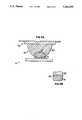
- FIG. 4is a graph of the temperature profile for a chip/substrate assembly during infrared reflow.
- FIG. 5ais a cross-sectional view of an electrical connection between a flip chip and a substrate.
- FIG. 5bis a cross-sectional, enlarged fragmented view of the copper/solder interface in the electrical connection of FIG. 5a.
- a number of flip chipsare electrically connected to an adhesiveless flexible printed circuit substrate.
- the preferred embodiment of the inventionincorporates automated processes to allow for higher tolerances, greater repeatability and higher productivity.
- a flip chipis an unpackaged silicon integrated circuit chip, such as flip chip 10, having a silicon chip 17 containing the integrated circuit components and coated with an active side passivation layer 11a on the active side 12 to protect its components from environmental contaminants. It has markings 13 applied to its back side 14 for identification purposes, and a back side passivation layer 11b coated on back side 14 to protect the markings. It also has a number of aluminum/copper bonding pads, such as bonding pad 15, which are located at various positions on the flip chip's active side for making electrical connections with a substrate. Solder bumps, such as solder bump 16, are further attached to these bonding pads.
- solder bumpsare attached to the bonding pads by a separate solder bump formation process which is typically performed during the manufacture of the flip chips.
- solder bump formation processesthere are a number of solder bump formation processes available in the art. One of these processes is shown in FIGS. 2a-d and described below. These figures are simply illustrative of the process, and are not drawn to scale, i.e. they do not reflect the actual dimensions or surface features of the various layers in the process.
- the flip chip 10has a layer of silicon 21 and a layer of silicon oxide 22 which make up silicon chip 17.
- openingsare cut into the active side passivation layer 11a of each of the flip chips on a wafer, to expose the bonding pads 15 located on active side 12 (FIG. 2a).
- Titanium/tungsten layer 23 and then copper layer 24are sputtered onto the entire active side of the wafer (FIG. 2b).
- the sputtered titanium/tungsten layerpromotes intermetallic adhesion, while the sputtered copper layer provides a surface to which an electroplated copper layer can attach.
- the continuous sputtered bilayer metallic sheetserves as the bus metal when the next two metal layers are electroplated over the bonding pads of the chip.
- Photoresistis then applied to the active side 12, and cuts are then made in the photoresist to expose the sputtered copper layer over the metal bonding pads. Copper 25 and then solder 26 is electroplated onto the exposed sputtered copper 24 (FIG. 2c). The photoresist layer is removed and the excess sputtered layers are wet etched away. Finally, the solder is heated and reflowed, to form a hemispherically-shaped solder bump 16 (FIG. 2d).
- solder bumpstypically have compositions ranging between a 3:97 and a 10:90 tin/lead ratio, requiring reflow temperatures in the range of 320° C.
- solder bumps having a 6:94 tin/lead ratioare used, which have a reflow temperature of approximately 316° C., and which we have found optimize both joint adhesion and solder ductility.
- the solder bumpsare also roughly hemispherical in shape, typically having a diameter of 9 mils (0.009") and a height of between 4 and 4.5 mils.
- the adhesiveless flexible printed circuit substrate usedis a Novaclad® substrate 30. It essentially consists of a polyimide film 31 having copper layers 32 secured on one or both surfaces thereon.
- Copper laminants 32are securely bonded to film 31 through a process as described in U.S. Pat. No. 5,112,462 to Swisher, assigned to the same assignee as the present application.
- the processessentially consists of (1) treating a film with a plasma made up of ionized oxygen produced from a metallic electrode to form a metal-oxide treated film, and (2) forming metallized interconnection layers on this treated film, preferably either by vacuum metalization of metal, or by a combination of vacuum metalization of metal and an additional step of electroplating metal on top of the vacuum-deposited metal.
- the first step in this processproduces a bonding surface on the film which is capable of securing metal interconnection layers which, unlike adhesive-based substrates, have excellent delamination resistance, even when exposed to heat, chemical treatment, mechanical stress or environmental stress.
- the method of the present inventionis applicable in general to other members of the class of adhesiveless flexible printed circuit substrates, such as polyester-based substrates, and other substrates produced using different methods.
- the method of the present inventionis also applicable to adhesive-based substrates, particularly when suitable solder pastes having reflow points within the tolerance ranges of the adhesive-based substrates be used.
- Novaclad® substratesoffer significant advantages over adhesive-based flexible substrates. They are less sensitive to adverse effects of solvents and moisture and don't have the tendency to become too sticky or too soft under certain operating conditions. Most importantly, they have a much wider range of operating temperatures due to the lack of the temperature-sensitive adhesives.
- Novaclad® substratesalso offer a significant advantage over ceramic substrates because the material polyimide is carefully matched to silicon to provide minimal shear force exposure to chips mounted on the substrate.
- the thermal coefficient of expansion of a polyimide substrate(80 ⁇ 10 -7 (° /C.)) is roughly similar to that of an alumina substrate (65 ⁇ 10 -7 (° /C.)); however, the modulus of polyimide substrate (61.8 ⁇ 10 4 psi) is several orders of magnitude lower than that of the alumina substrate (37 ⁇ 10 6 psi).
- These properties of the polyimide substratesignificantly reduce the formation of any damaging shear forces, during heating/cooling cycles, between the chip and the substrate which could fracture the interconnects.
- the shear forces for a silicon flip chip connected to a polyimide substrateare:
- the copper layers 31contain an interconnection pattern for the circuit to be assembled, with a number of contact pads, such as contact pad 33, defined thereon, corresponding to the connection footprints, such as footprint 34, for the flip chips which may be connected to the substrate.
- a substrate containing one interconnection patternmay be useful for more than one assembled circuit, and as a flip chip may be useful for more than one assembled circuit, it is not required that every contact pad correspond to a solder bump or vice versa.
- Active contact padsare the contact pads on the substrate which do have corresponding solder bumps. These active pads are the only contact pads which are electrically connected to solder bumps by the method of the present invention.
- the first step of the methodis to provide solder paste to each of the active contact pads on the substrate.
- the solder pastetypically is a composition of solder in a carrier matrix of flux.
- the particular compositionis chosen to have a viscosity value for easy registration of the paste through the stencil and onto the substrate, while having a solder content sufficient to form electrical connections with the flip chips.
- the solder paste chosen for a preferred embodimentis ALPHA WS-601 solder paste, manufactured by Alphametals of Jersey City, N.J. This preferred paste is a 90% metal material having a viscosity around 900 kcps, which is typically lower than most solder pastes due to the smaller openings in the stencil that are required for the method of the present invention.
- the flux used in this pasteis a halide free, neutralized organic acid flux system, which allows for easy and thorough residue removal.
- solder composition in the pasteis a 63:37 eutectic alloy of tin:lead formed in spherical particles having diameters no larger than 45 microns.
- the particlesmust be smaller than those in most solder paste, due to the smaller openings in the stencil that are required for the method of the present invention.
- Solder having this composition of materialshas a reflow temperature in the range of 183° C.
- solder pastewhich is compatible with another preferred embodiment of the invention is a 90% metal composition having 700 kcps viscosity, with the solder composition in the paste being a 63:35:2 eutectic alloy of tin:lead:silver formed in spherical particles having diameters no larger than 45 microns.
- Solder having this composition of materialshas a similar reflow temperature, in the range of 182° C.
- compositions of solder pastemay be used in the method of the present invention, such as solder pastes produced by Kester or Multicore, for example. Due to the lack of temperature constraints on the Novaclad® substrate, the solder alloy is not limited to eutectic compositions having low melting points as required by adhesive based flexible substrates, such as in the Legg et al. reference. Compositions of solder which have reflow temperatures which are below, or which meet or exceed that of, the solder bumps on the flip chips may be used in the method of the present invention.
- Lower temperature solder compositionssuch as those used in the above preferred embodiments, have the advantage of being used with a wide variety of electrical components. This is due primarily to the fact that reflow of these compositions induces less thermal stress on electrical components, so more standard components are capable of withstanding the reflow process.
- the use of higher temperature solder compositions in the method of the present inventionprovides further advantages.
- One such advantageis the ability for the method of the present invention to implement higher temperature reflow processes, such as vapor phase oven reflow processes using higher temperature vapor phase heat transfer solvents.
- higher temperature solder compositionsmay allow assemblies created using the method of the present invention to be more resistant to temperature exposure in high temperature applications. Though soldered connections formed by many prior art methods are unable to sustain high temperatures without reflowing, the higher temperature solder compositions capable of being implemented in the method of the present invention would require much higher temperatures in order to reflow. Therefore, assemblies having high temperature components electrically connected by the present invention's method would be capable of being used in a wide range of operating environments.
- a preferred high temperature solder pastewould have a solder composition similar to that of the solder bumps themselves, preferrably being tin-lead solder with a tin content between 3% and 10%, and more preferrably being tin-lead solder having 6% tin and 94% lead.
- the volume of solder paste applied to each active contact padis critical to the success of the method. This critical volume is dependent primarily on the area of the active contact pad, the connected distance between the substrate and the corresponding flip chip in final assembled form, and the volume of the corresponding solder bump. This volume may be found by subtracting the volume of the solder bump from the volume of the desired electrical connection (also called a solder filet) to obtain the desired volume of solder, and then calculating the volume of solder paste which would contain this volume of solder.
- solder bumps having a 9 mil diameterfor a 5 mil connected distance between the substrate and the flip chip, for a 12 mil contact pad diameter, and for a 90% metal composition of solder paste, the optimal volume of solder paste was approximately 6 ⁇ 10 -7 in 3 .
- the step of providing solder pasteis performed by stencilling the solder paste onto the substrate through a stencil.
- the stencilis a brass sheet having etched openings to allow solder paste to pass through to register onto active contact pads.
- the etched patternis produced from a CAD layer generated with the circuit artwork, making the pattern a perfect match to the substrate.
- the stencilling stepis an automated process, where fiducial registration is used to align the stencil with the substrate to provide precise registration of the solder paste on the substrate.
- Fiducial registrationis provided by optical alignment, where first a camera finds fiducial marks (typically black dots in the center of black outlined circles) on both the stencil and the substrate, and then the stencil is aligned precisely over the substrate based upon the calculations of alignment errors found by the camera.
- the alignment of the stencilcan be critical to the success of the method, as the stencil can not be off by more than a couple of mils given the size of the solder bumps (9 mil diameter).
- a quantity of solder pasteis provided along the top surface of the stencil and a squeegee of specified hardness, speed, and pressure travels over the stencil to force the solder paste through the openings in the stencil and onto the active contact pads on the substrate.
- the stencilis then removed, leaving a substrate containing the precise amount of solder paste on each active contact pad.
- the amount of solder paste provided to each active contact padis dependent upon a number of factors during this step, so each must be carefully controlled to assure repeatable results for the method. Specifically, the volume of solder paste is primarily dependent upon the diameter of the etched opening, the thickness of the stencil, the pressure applied by the squeegee, the hardness of the squeegee, and the speed of the squeegee. The optimal values for these factors were found by using a test stencil of various thicknesses and opening diameters to register solder paste to a non-wettable polyimide substrate, reflowing the solder paste to form solder balls (as the solder could not wet to the substrate), and measuring the volume of the resulting solder balls.
- solder pastefor the preferred embodiment of the invention, it was found that a 4 mil thick stencil having 14 mil diameter openings was desired. It was found that the desired squeegee was a round squeegee having a 90 durometer hardness, travelling at a speed of 1.5 inches/second and applying a downward pressure of 22 psi to the stencil.
- the second step of the methodis to place each of the chips onto the substrate such that the solder paste on each active pad is in registration with the corresponding solder bump on a flip chip, to form an unsoldered chip/substrate assembly.
- optical placement equipmentis used to place the chips one-by-one onto the substrate. Such equipment is computer-controlled, which allows for programs to be stored for each type of circuit to be assembled, to provide for completely automated chip registration.
- This equipmentplaces chips and other components which are provided in a tape and reel format; however, it is also capable of placing chips and components which are provided in other formats typically usable with automated placement equipment, such as in a waffle pack format.
- This equipmentalso uses the fiducial registration marks on the substrate to properly align the chips to the substrate before registration.
- the fiducial marks on the substrateare located by optical means prior to placement, so that the equipment can compensate for misalignment of the substrate in the equipment, as well as stretching, shrinkage or angularity variations between points on the substrate itself.
- the equipmenthas robotic arms which pick and place the parts on the substrate, and it also allows for the parts to be examined by a camera before placement on the substrate, to correct for x,y and rotational misalignment of the parts on the robotic arms.
- the third stepis to heat the chip/substrate assembly as a whole.
- the heating means used to affect this stepis either of a type operating by direct infrared radiation, or by transmission of heat from a heated working fluid.
- the solder paste on every active contact padreflows and forms an electrical connection with its corresponding solder bump, so that each chip is electrically connected to the substrate.
- the heating meansis an infrared (IR) reflow oven.
- the oveninduces reflow of the solder paste by subjecting the unsoldered chip/substrate assembly to direct infrared radiation from both the top and bottom of the oven.
- the infrared reflow ovenmay have a nitrogen purge option in its heated zones, to inhibit the formation of solder oxides during reflow, and consequently, provide for a higher quality electrical connection.
- the unsoldered chip/substrate assemblyis placed on a palette and passed through the oven by a conveyor.
- the oven and conveyorare computer-controlled, which allows for precise control of heating rates, conveyor speed, and alarms.
- Product specific recipesmay be stored in the computer, so that a carefully controlled and repeatable temperature profile for the reflow process of a particular assembly may be specifically tailored to the assembly, based upon such factors as materials used, component sizes, and component densities.
- an unsoldered chip/substrate assemblyis passed through the infrared reflow oven at a specific rates and temperatures, based upon the temperature profile for the particular assembly.
- the entire assemblyis subjected to the heating means simultaneously, and heat reaches each of the solder paste/solder bump interfaces directly, so that reflow of the solder paste, and the subsequent formation of an electrical connection at each interface occurs concurrently.
- thermode method of heatingThis method is superior to the thermode method of heating first because of the decreased thermal stress imposed on the chips.
- heatreaches the solder paste/solder bump interfaces on the assembly directly, rather than through the active components of the chips. Consequently, the durability and performance requirements are not as substantial as they are for chips usable with the thermode method.
- Chips for use with the thermode method of heatingmust be constructed to high performance specifications, which, due to the increased costs involved, make that method unsuitable for many lower-cost applications. Chips for use with the method of the present invention, however, need not be designed and constructed with the same performance specifications, and therefore, the method ends up being significantly more cost-effective for a broader range of applications.
- thermode methodthe thermode must remain in contact with a chip for a fixed period of time in order to reflow that chip.
- the time to reflow the entire assemblyincreases proportionally.
- the time to form electrical connections by the method of the present inventionis reduced, as all connections between the chips and substrate are formed concurrently, rather than individually. In fact, as the number of chips on an assembly increases, the benefits of this method over the thermode method increase accordingly.
- An IR reflow oven for use with the method of the present inventionis divided into three heating zones, with individual control of heating from top and bottom.
- a preferred temperature profileis shown in FIG. 4.
- the assemblymoves through each zone of the oven at the rate of 32.4 inches/minute.
- the first zoneis the first preheat zone 40, which ramps the temperature of the assembly from the ambient temperature up to approximately 20°-30° C. below the reflow temperature of the solder in the solder paste (150° C. for the solder paste of the preferred embodiment).
- the purpose of this zoneis to bring the assembly close to the reflow temperature without introducing shear forces generated by differing thermal coefficients of expansion of the various parts of the assembly, and to dry out the solder paste (i.e. remove the solvents).
- a short heat soak zone 41may also be included before the second zone, where the heating is temporarily decreased in order for the entire assembly to reach the same temperature.
- the second zoneis the second preheat zone 42, which raises the temperature of the assembly to just below the reflow temperature of the solder (175°-180° C. for the solder paste of the preferred embodiment).
- the purpose of this zoneis to activate and release the fluxes in the solder paste just prior to reflow, so that the solder is the only component left in the paste.
- the third and last zone in the temperature profileis the reflow zone 43, which raises the temperature of the assembly above the reflow temperature of the solder, to a peak of approximately 40° C. above the reflow temperature (225° C. for the solder paste of the preferred embodiment).
- the purpose of this zoneis to reflow the solder left from the solder paste to form the electrical connections.
- the peakmust extend above the reflow temperature of the solder because the solder bump/contact pad interfaces are not subjected to direct IR due to their placement between the active side of the chips and the substrate.
- the assemblyenters a cooling zone 44 where the electrical connections are allowed to solidify and the assembly is allowed to return to ambient temperature.
- Alternative heating meansmay also be effective when used in conjunction with the method of the present invention which, in lieu of subjecting the assembly to direct infrared radiation, transmit heat to the assembly through a heated working fluid.
- One alternative heating meansis a convection reflow oven, in which heat is generated by heating elements and transmitted by convection through circulated air to the assembly.
- a similar temperature profile to the IR reflow profile of FIG. 4would be used in such an oven, with corrections made for differing rates of heat, and for the fact that the solder bump/contact pad interface would be more directly exposed to the convection heating process.
- Another alternative heating meansis a vapor phase reflow oven, in which heat is also generated by heating elements, but is transmitted by convection through another working fluid which has its vapor point above the reflow temperature of the solder.
- a vapor phase reflow ovenin which heat is also generated by heating elements, but is transmitted by convection through another working fluid which has its vapor point above the reflow temperature of the solder.
- One such fluid usable in a preferred embodiment of the inventionis Fluorinert FC-70
- this type of ovenIn this type of oven, the unsoldered assembly is moved by conveyor into a closed chamber, and the entire assembly is exposed to the high-temperature vapor. While the temperature of the assembly is below the vapor point of the working fluid, the fluid condenses on the assembly and transfers its heat to the assembly. Because the vapor must have a vapor point above reflow temperature, a different temperature profile is required for such an oven, and preheat cannot be accomplished through gradual heating. Therefore, this type of oven does not allow for the same degree of control of heating temperatures and rates as provided by the other two ovens, and is unable to prevent shear forces in the same manner. This type of oven is, in general, more demanding on the assemblies than the other ovens described above.
- an additional stepmay be applied to the completed assembly to decrease the probability of defects.
- the entire completed assemblymay be cleaned using one of the commonly known cleaning techniques for printed circuit assemblies.
- the method of cleaningis of special importance to flip chip applications, because care must be taken to thoroughly clean between the chip and the substrate, as stray solder particles could become lodged in the gap and induce short circuits across electrical connections.
- the preferred method of cleaninginvolves cleaning the assembly with a freon-based solvent, such as any of the various liquid chlorofluorocarbon (CFC) solvents, or vapors of these materials, in order to dissolve and flush away solder flux residues.
- the preferred methodalso includes the use of ultrasonic agitation of these solvents to improve the ability of the solvents to dissolve and flush away the residues.
- freon-based solventsexamples include Genesolv DFX distributed by Worum Chemical, or Freon solvents manufactured by DuPont.
- Solvent DFXdistributed by Worum Chemical
- Freon solvents manufactured by DuPontexamples include Genesolv DFX distributed by Worum Chemical, or Freon solvents manufactured by DuPont.
- other cleaning processesmay be used, depending upon the particular solder paste and flux compositions used, such as semi-aqueous or fully aqueous solutions, with or without ultrasonic agitation.
- the formation of the electrical connections, such as electrical connection 50, between a flip chip 10 and a substrate 30is described.
- the figures, however,are merely representative of the compositions within the electrical connections, and are not drawn to scale.
- the solder pasteis dried out (i.e. the solvents are removed) and its fluxes are activated, leaving only particles of solder on each contact pad.
- these particlesliquify and form molten solder masses on the contact pads.
- the chipis suspended on the molten solder masses, and is allowed to self-align into its proper location and orientation on the substrate.
- solder bumpsAfter the solder particles liquify, the solder bumps then begin to dissolve into the molten solder masses and form solder compositions of the solder from the bumps and the paste along the interfaces, because the solder in the solder bumps and the solder from the solder particles are readily miscible.
- the solder compositions in the interfaces between the solder bumps and the molten solder masseschange due to the dissolution of the solder bumps, and the reflow point of the resulting solder compositions begin to increase.
- homogeneous solder compositions 53are reached, and electrical connections 50 solidify, because the reflow point has increased beyond the temperature of the assembly in the oven.
- the flip chipis electrically connected to the substrate.
- an interface layer 52is formed between solder 53 and the copper pedestal 51.
- the strength of the connectionscan be attributed to a number of factors.
- the firstis the fact that the reflow oven method of heating allows for unobstructed motion of the chips in relation to the substrate during reflow, so that the chips are allowed to self-align to their proper location and orientation on the substrate.
- Another factoris the composition of the solder paste, which we found produced electrical connections having a homogeneous mixture of solder throughout, with few undesired crystalline microstructures or other deformities.
- Assemblies produced by the method of the present inventionwere also subjected to thermal cycling, in order determine the ability of the connections to withstand thermal stress.
- Test assemblieswere placed in an air-to-air thermal chamber and cycled between -65° C. and 150° C., remaining 20 minutes at each temperature and spending 20 seconds in transit between chambers. It was found that 75% of these assemblies had intermittent contacts, most formed along the tin-copper interface of an electrical connection (as shown in FIG. 5b), after 200 cycles.
- the thermal cycling performance of the method of the present inventioncan be attributed to a number of factors.
- the aforementioned self-alignment properties and choice of solder pasteplay a great role in this characteristic.
- the superiority of the Novaclad® substrate over ceramic substratesis also significant. This is primarily because the shear forces from thermal expansion for the flexible substrate (3.09 psi/° C.) are significantly lower than those for the ceramic substrate (129.5 psi/° C.). Consequently, thermal changes tend to introduce less shear forces on chips mounted on a flexible substrate than those on a ceramic substrate, so the assemblies are better able to withstand thermal cycling.
- the method of the present inventionis thus useful for mounting flip chips to a flexible substrate in a reliable, cost-efficient manner.
- the electrical connections formed by the methodmeet or exceed the reliability and performance characteristics of those formed by most existing methods.
- due to the method's ability to form electrical connections without a great deal of thermal stress, less expensive, lower performance chipsmay be used in conjunction with the method, allowing it to be used in a wider variety of lower-cost and consumer applications.
- the productivity of the methodis preferred over many existing methods as many of the steps are batch processes which operate concurrently on entire assemblies.
- the methodmay be implemented using standard surface-mount technology equipment, it may be incorporated into existing facilities at a reasonable cost.
- assembliesmay be produced which have higher resistance to temperature, and which therefore may be used in a wide variety of specialized applications in more hostile operating environments. All that would be required in such circumstances would be flip chips which were capable of withstanding the increased operating temperatures.
Landscapes
- Engineering & Computer Science (AREA)
- Microelectronics & Electronic Packaging (AREA)
- Computer Hardware Design (AREA)
- Power Engineering (AREA)
- Physics & Mathematics (AREA)
- Condensed Matter Physics & Semiconductors (AREA)
- General Physics & Mathematics (AREA)
- Manufacturing & Machinery (AREA)
- Wire Bonding (AREA)
- Electric Connection Of Electric Components To Printed Circuits (AREA)
Abstract
Description
E.sub.substrate ×(TCE.sub.substrate -TCE.sub.silicon die)=psi/° C.
(37×10.sup.6 (psi))×(65×10.sup.-7 (° /C.)-30×10.sup.-7 (° /C.))=129.5 psi/° C.
E.sub.substrate ×(TCE.sub.substrate -TCE.sub.silicon die)=psi/° C.
(61.8×10.sup.4 (psi))×(65×10.sup.-7 (° /C.)-30×10.sup.-7 (° /C.))=3.09 psi/° C.
Claims (25)
Priority Applications (2)
| Application Number | Priority Date | Filing Date | Title |
|---|---|---|---|
| US07/932,064US5261593A (en) | 1992-08-19 | 1992-08-19 | Direct application of unpackaged integrated circuit to flexible printed circuit |
| US08/081,544US5349500A (en) | 1992-08-19 | 1993-06-23 | Direct application of unpackaged integrated circuit to flexible printed circuit |
Applications Claiming Priority (1)
| Application Number | Priority Date | Filing Date | Title |
|---|---|---|---|
| US07/932,064US5261593A (en) | 1992-08-19 | 1992-08-19 | Direct application of unpackaged integrated circuit to flexible printed circuit |
Related Child Applications (1)
| Application Number | Title | Priority Date | Filing Date |
|---|---|---|---|
| US08/081,544DivisionUS5349500A (en) | 1992-08-19 | 1993-06-23 | Direct application of unpackaged integrated circuit to flexible printed circuit |
Publications (1)
| Publication Number | Publication Date |
|---|---|
| US5261593Atrue US5261593A (en) | 1993-11-16 |
Family
ID=25461706
Family Applications (2)
| Application Number | Title | Priority Date | Filing Date |
|---|---|---|---|
| US07/932,064Expired - LifetimeUS5261593A (en) | 1992-08-19 | 1992-08-19 | Direct application of unpackaged integrated circuit to flexible printed circuit |
| US08/081,544Expired - LifetimeUS5349500A (en) | 1992-08-19 | 1993-06-23 | Direct application of unpackaged integrated circuit to flexible printed circuit |
Family Applications After (1)
| Application Number | Title | Priority Date | Filing Date |
|---|---|---|---|
| US08/081,544Expired - LifetimeUS5349500A (en) | 1992-08-19 | 1993-06-23 | Direct application of unpackaged integrated circuit to flexible printed circuit |
Country Status (1)
| Country | Link |
|---|---|
| US (2) | US5261593A (en) |
Cited By (117)
| Publication number | Priority date | Publication date | Assignee | Title |
|---|---|---|---|---|
| US5346118A (en)* | 1993-09-28 | 1994-09-13 | At&T Bell Laboratories | Surface mount solder assembly of leadless integrated circuit packages to substrates |
| EP0632685A3 (en)* | 1993-06-03 | 1995-05-17 | Ibm | Flexible circuit board assembly with common heat spreader and method of manufacture. |
| US5539153A (en)* | 1994-08-08 | 1996-07-23 | Hewlett-Packard Company | Method of bumping substrates by contained paste deposition |
| US5547740A (en)* | 1995-03-23 | 1996-08-20 | Delco Electronics Corporation | Solderable contacts for flip chip integrated circuit devices |
| US5553538A (en)* | 1995-01-30 | 1996-09-10 | Motorola, Inc. | Method and apparatus for stencil printing printed circuit boards |
| US5607099A (en)* | 1995-04-24 | 1997-03-04 | Delco Electronics Corporation | Solder bump transfer device for flip chip integrated circuit devices |
| US5615824A (en)* | 1994-06-07 | 1997-04-01 | Tessera, Inc. | Soldering with resilient contacts |
| US5615477A (en)* | 1994-09-06 | 1997-04-01 | Sheldahl, Inc. | Method for interconnecting a flip chip to a printed circuit substrate |
| US5632631A (en)* | 1994-06-07 | 1997-05-27 | Tessera, Inc. | Microelectronic contacts with asperities and methods of making same |
| US5660321A (en)* | 1996-03-29 | 1997-08-26 | Intel Corporation | Method for controlling solder bump height and volume for substrates containing both pad-on and pad-off via contacts |
| WO1997040530A1 (en)* | 1996-04-19 | 1997-10-30 | Motorola Inc. | Solder bump apparatus, electronic component and method for forming a solder bump |
| US5719749A (en)* | 1994-09-26 | 1998-02-17 | Sheldahl, Inc. | Printed circuit assembly with fine pitch flexible printed circuit overlay mounted to printed circuit board |
| US5729440A (en)* | 1995-05-25 | 1998-03-17 | International Business Machines Corporation | Solder hierarchy for chip attachment to substrates |
| US5802699A (en)* | 1994-06-07 | 1998-09-08 | Tessera, Inc. | Methods of assembling microelectronic assembly with socket for engaging bump leads |
| US5872051A (en)* | 1995-08-02 | 1999-02-16 | International Business Machines Corporation | Process for transferring material to semiconductor chip conductive pads using a transfer substrate |
| US5931371A (en)* | 1997-01-16 | 1999-08-03 | Ford Motor Company | Standoff controlled interconnection |
| US5960251A (en)* | 1996-04-18 | 1999-09-28 | International Business Machines Corporation | Organic-metallic composite coating for copper surface protection |
| US5971249A (en)* | 1997-02-24 | 1999-10-26 | Quad Systems Corporation | Method and apparatus for controlling a time/temperature profile inside of a reflow oven |
| US5983492A (en)* | 1996-11-27 | 1999-11-16 | Tessera, Inc. | Low profile socket for microelectronic components and method for making the same |
| US6036836A (en)* | 1996-12-20 | 2000-03-14 | Peeters; Joris Antonia Franciscus | Process to create metallic stand-offs on an electronic circuit |
| US6056190A (en)* | 1997-02-06 | 2000-05-02 | Speedline Technologies, Inc. | Solder ball placement apparatus |
| US6077725A (en)* | 1992-09-03 | 2000-06-20 | Lucent Technologies Inc | Method for assembling multichip modules |
| US6111324A (en)* | 1998-02-05 | 2000-08-29 | Asat, Limited | Integrated carrier ring/stiffener and method for manufacturing a flexible integrated circuit package |
| US6147870A (en)* | 1996-01-05 | 2000-11-14 | Honeywell International Inc. | Printed circuit assembly having locally enhanced wiring density |
| US6162661A (en)* | 1997-05-30 | 2000-12-19 | Tessera, Inc. | Spacer plate solder ball placement fixture and methods therefor |
| US6170737B1 (en) | 1997-02-06 | 2001-01-09 | Speedline Technologies, Inc. | Solder ball placement method |
| EP1035579A3 (en)* | 1999-03-05 | 2001-03-07 | Altera Corporation | Fabrication method and strcuture of an integrated circuit package |
| US6201193B1 (en)* | 1994-05-06 | 2001-03-13 | Seiko Epson Corporation | Printed circuit board having a positioning marks for mounting at least one electronic part |
| US6202918B1 (en) | 1997-01-28 | 2001-03-20 | Eric Hertz | Method and apparatus for placing conductive preforms |
| US6226183B1 (en)* | 1997-08-25 | 2001-05-01 | Robert Bosch Gmbh | Arrangement including a substrate for power components and a heat sink, and a method for manufacturing the arrangement |
| US6230963B1 (en) | 1997-01-28 | 2001-05-15 | Eric L. Hertz | Method and apparatus using colored foils for placing conductive preforms |
| US6246014B1 (en) | 1996-01-05 | 2001-06-12 | Honeywell International Inc. | Printed circuit assembly and method of manufacture therefor |
| US6276599B1 (en)* | 1998-04-10 | 2001-08-21 | Noda Screen Co., Ltd. | Method and apparatus for forming solder bumps |
| US6287893B1 (en) | 1997-10-20 | 2001-09-11 | Flip Chip Technologies, L.L.C. | Method for forming chip scale package |
| US6316830B1 (en) | 1998-12-17 | 2001-11-13 | Charles Wen Chyang Lin | Bumpless flip chip assembly with strips and via-fill |
| US6319751B1 (en) | 1998-12-17 | 2001-11-20 | Charles Wen Chyang Lin | Bumpless flip chip assembly with solder via |
| US6335563B1 (en)* | 1998-07-06 | 2002-01-01 | Seiko Epson Corporation | Semiconductor device, method of fabricating the same, circuit board, and electronic device |
| US6350632B1 (en) | 2000-09-20 | 2002-02-26 | Charles W. C. Lin | Semiconductor chip assembly with ball bond connection joint |
| US6350386B1 (en) | 2000-09-20 | 2002-02-26 | Charles W. C. Lin | Method of making a support circuit with a tapered through-hole for a semiconductor chip assembly |
| US6350633B1 (en) | 2000-08-22 | 2002-02-26 | Charles W. C. Lin | Semiconductor chip assembly with simultaneously electroplated contact terminal and connection joint |
| EP1081990A3 (en)* | 1999-09-06 | 2002-03-20 | Micro-Tec Company, Ltd. | A method for forming a solder ball |
| US6403400B2 (en) | 1998-12-17 | 2002-06-11 | Charles Wen Chyang Lin | Bumpless flip chip assembly with strips-in-via and plating |
| US6403460B1 (en) | 2000-08-22 | 2002-06-11 | Charles W. C. Lin | Method of making a semiconductor chip assembly |
| US6402970B1 (en) | 2000-08-22 | 2002-06-11 | Charles W. C. Lin | Method of making a support circuit for a semiconductor chip assembly |
| US6406939B1 (en) | 1998-05-02 | 2002-06-18 | Charles W. C. Lin | Flip chip assembly with via interconnection |
| US6424037B1 (en)* | 1999-11-30 | 2002-07-23 | Aptos Corporation | Process to make a tall solder ball by placing a eutectic solder ball on top of a high lead solder ball |
| US6436734B1 (en) | 2000-08-22 | 2002-08-20 | Charles W. C. Lin | Method of making a support circuit for a semiconductor chip assembly |
| US6440835B1 (en) | 2000-10-13 | 2002-08-27 | Charles W. C. Lin | Method of connecting a conductive trace to a semiconductor chip |
| US6444489B1 (en) | 2000-12-15 | 2002-09-03 | Charles W. C. Lin | Semiconductor chip assembly with bumped molded substrate |
| US6448644B1 (en) | 1998-05-02 | 2002-09-10 | Charles W. C. Lin | Flip chip assembly with via interconnection |
| US6448108B1 (en) | 2000-10-02 | 2002-09-10 | Charles W. C. Lin | Method of making a semiconductor chip assembly with a conductive trace subtractively formed before and after chip attachment |
| US6492252B1 (en) | 2000-10-13 | 2002-12-10 | Bridge Semiconductor Corporation | Method of connecting a bumped conductive trace to a semiconductor chip |
| US6511865B1 (en) | 2000-09-20 | 2003-01-28 | Charles W. C. Lin | Method for forming a ball bond connection joint on a conductive trace and conductive pad in a semiconductor chip assembly |
| US6527164B1 (en)* | 2000-05-31 | 2003-03-04 | Advanced Micro Devices, Inc. | Removing flux residue from reflow furnace using active gaseous solvent |
| US6537851B1 (en) | 2000-10-13 | 2003-03-25 | Bridge Semiconductor Corporation | Method of connecting a bumped compliant conductive trace to a semiconductor chip |
| US6544813B1 (en) | 2000-10-02 | 2003-04-08 | Charles W. C. Lin | Method of making a semiconductor chip assembly with a conductive trace subtractively formed before and after chip attachment |
| US6548393B1 (en) | 2000-10-13 | 2003-04-15 | Charles W. C. Lin | Semiconductor chip assembly with hardened connection joint |
| US6551861B1 (en) | 2000-08-22 | 2003-04-22 | Charles W. C. Lin | Method of making a semiconductor chip assembly by joining the chip to a support circuit with an adhesive |
| US6562657B1 (en) | 2000-08-22 | 2003-05-13 | Charles W. C. Lin | Semiconductor chip assembly with simultaneously electrolessly plated contact terminal and connection joint |
| US6562709B1 (en) | 2000-08-22 | 2003-05-13 | Charles W. C. Lin | Semiconductor chip assembly with simultaneously electroplated contact terminal and connection joint |
| US6576493B1 (en) | 2000-10-13 | 2003-06-10 | Bridge Semiconductor Corporation | Method of connecting a conductive trace and an insulative base to a semiconductor chip using multiple etch steps |
| US6576539B1 (en) | 2000-10-13 | 2003-06-10 | Charles W.C. Lin | Semiconductor chip assembly with interlocked conductive trace |
| WO2002061834A3 (en)* | 2001-01-30 | 2003-06-12 | Murata Manufacturing Co | Electronic part |
| US6578755B1 (en) | 2000-09-22 | 2003-06-17 | Flip Chip Technologies, L.L.C. | Polymer collar for solder bumps |
| US6583040B1 (en) | 2000-10-13 | 2003-06-24 | Bridge Semiconductor Corporation | Method of making a pillar in a laminated structure for a semiconductor chip assembly |
| US20030127734A1 (en)* | 2002-01-07 | 2003-07-10 | Jin-Yuan Lee | Cylindrical bonding structure and method of manufacture |
| US6598779B2 (en)* | 2000-06-15 | 2003-07-29 | Murata Manufacturing Co., Ltd. | Electronic component mounting method |
| US6641030B1 (en) | 1997-02-06 | 2003-11-04 | Speedline Technologies, Inc. | Method and apparatus for placing solder balls on a substrate |
| US6644536B2 (en)* | 2001-12-28 | 2003-11-11 | Intel Corporation | Solder reflow with microwave energy |
| US6653170B1 (en) | 2001-02-06 | 2003-11-25 | Charles W. C. Lin | Semiconductor chip assembly with elongated wire ball bonded to chip and electrolessly plated to support circuit |
| US6660626B1 (en) | 2000-08-22 | 2003-12-09 | Charles W. C. Lin | Semiconductor chip assembly with simultaneously electrolessly plated contact terminal and connection joint |
| US6667229B1 (en) | 2000-10-13 | 2003-12-23 | Bridge Semiconductor Corporation | Method of connecting a bumped compliant conductive trace and an insulative base to a semiconductor chip |
| US6666810B1 (en)* | 1999-06-11 | 2003-12-23 | Honeywell International Inc. | Device for controllable stretching of thin materials |
| US6699780B1 (en) | 2000-10-13 | 2004-03-02 | Bridge Semiconductor Corporation | Method of connecting a conductive trace to a semiconductor chip using plasma undercut etching |
| US6740576B1 (en) | 2000-10-13 | 2004-05-25 | Bridge Semiconductor Corporation | Method of making a contact terminal with a plated metal peripheral sidewall portion for a semiconductor chip assembly |
| US20040099960A1 (en)* | 2001-04-05 | 2004-05-27 | Sylvia Adae-Amoakoh | Economical high density chip carrier |
| US20040099716A1 (en)* | 2002-11-27 | 2004-05-27 | Motorola Inc. | Solder joint reliability by changing solder pad surface from flat to convex shape |
| US20040108600A1 (en)* | 2001-12-28 | 2004-06-10 | Jimmy Liang | Method and apparatus for flip chip device assembly by radiant heating |
| US20040121626A1 (en)* | 2002-09-26 | 2004-06-24 | Fci Americas Technology, Inc. | Surface mounted electrical components and method for mounting and retaining same |
| US6805278B1 (en) | 1999-10-19 | 2004-10-19 | Fci America Technology, Inc. | Self-centering connector with hold down |
| US6872591B1 (en) | 2000-10-13 | 2005-03-29 | Bridge Semiconductor Corporation | Method of making a semiconductor chip assembly with a conductive trace and a substrate |
| US6876072B1 (en) | 2000-10-13 | 2005-04-05 | Bridge Semiconductor Corporation | Semiconductor chip assembly with chip in substrate cavity |
| US6908788B1 (en) | 2000-10-13 | 2005-06-21 | Bridge Semiconductor Corporation | Method of connecting a conductive trace to a semiconductor chip using a metal base |
| US6949408B1 (en) | 2000-10-13 | 2005-09-27 | Bridge Semiconductor Corporation | Method of connecting a conductive trace and an insulative base to a semiconductor chip using multiple etch steps |
| US6984576B1 (en) | 2000-10-13 | 2006-01-10 | Bridge Semiconductor Corporation | Method of connecting an additively and subtractively formed conductive trace and an insulative base to a semiconductor chip |
| US7009297B1 (en) | 2000-10-13 | 2006-03-07 | Bridge Semiconductor Corporation | Semiconductor chip assembly with embedded metal particle |
| US7057292B1 (en) | 2000-05-19 | 2006-06-06 | Flipchip International, Llc | Solder bar for high power flip chips |
| US7071089B1 (en) | 2000-10-13 | 2006-07-04 | Bridge Semiconductor Corporation | Method of making a semiconductor chip assembly with a carved bumped terminal |
| US7075186B1 (en) | 2000-10-13 | 2006-07-11 | Bridge Semiconductor Corporation | Semiconductor chip assembly with interlocked contact terminal |
| US7094676B1 (en) | 2000-10-13 | 2006-08-22 | Bridge Semiconductor Corporation | Semiconductor chip assembly with embedded metal pillar |
| US7112521B1 (en) | 2000-10-13 | 2006-09-26 | Bridge Semiconductor Corporation | Method of making a semiconductor chip assembly with a bumped metal pillar |
| US7129113B1 (en) | 2000-10-13 | 2006-10-31 | Bridge Semiconductor Corporation | Method of making a three-dimensional stacked semiconductor package with a metal pillar in an encapsulant aperture |
| US7132741B1 (en) | 2000-10-13 | 2006-11-07 | Bridge Semiconductor Corporation | Semiconductor chip assembly with carved bumped terminal |
| US7190080B1 (en) | 2000-10-13 | 2007-03-13 | Bridge Semiconductor Corporation | Semiconductor chip assembly with embedded metal pillar |
| US20070161234A1 (en)* | 2006-01-11 | 2007-07-12 | Rinne Glenn A | Methods of Forming Back Side Layers for Thinned Wafers and Related Structures |
| US7262082B1 (en) | 2000-10-13 | 2007-08-28 | Bridge Semiconductor Corporation | Method of making a three-dimensional stacked semiconductor package with a metal pillar and a conductive interconnect in an encapsulant aperture |
| US7264991B1 (en) | 2000-10-13 | 2007-09-04 | Bridge Semiconductor Corporation | Method of connecting a conductive trace to a semiconductor chip using conductive adhesive |
| US7268421B1 (en) | 2004-11-10 | 2007-09-11 | Bridge Semiconductor Corporation | Semiconductor chip assembly with welded metal pillar that includes enlarged ball bond |
| US7319265B1 (en) | 2000-10-13 | 2008-01-15 | Bridge Semiconductor Corporation | Semiconductor chip assembly with precision-formed metal pillar |
| US20080135990A1 (en)* | 2006-12-07 | 2008-06-12 | Texas Instruments Incorporated | Stress-improved flip-chip semiconductor device having half-etched leadframe |
| US7396703B1 (en) | 2003-11-20 | 2008-07-08 | Bridge Semiconductor Corporation | Method of making a semiconductor chip assembly with a bumped terminal and a filler |
| US7414319B2 (en) | 2000-10-13 | 2008-08-19 | Bridge Semiconductor Corporation | Semiconductor chip assembly with metal containment wall and solder terminal |
| US7446419B1 (en) | 2004-11-10 | 2008-11-04 | Bridge Semiconductor Corporation | Semiconductor chip assembly with welded metal pillar of stacked metal balls |
| US7446399B1 (en) | 2004-08-04 | 2008-11-04 | Altera Corporation | Pad structures to improve board-level reliability of solder-on-pad BGA structures |
| US20090014502A1 (en)* | 2003-03-10 | 2009-01-15 | Motoyuki Itoh | Method and apparatus for placing conductive balls |
| US7494843B1 (en) | 2006-12-26 | 2009-02-24 | Bridge Semiconductor Corporation | Method of making a semiconductor chip assembly with thermal conductor and encapsulant grinding |
| US7538415B1 (en) | 2003-11-20 | 2009-05-26 | Bridge Semiconductor Corporation | Semiconductor chip assembly with bumped terminal, filler and insulative base |
| US7750483B1 (en) | 2004-11-10 | 2010-07-06 | Bridge Semiconductor Corporation | Semiconductor chip assembly with welded metal pillar and enlarged plated contact terminal |
| US7811863B1 (en) | 2006-10-26 | 2010-10-12 | Bridge Semiconductor Corporation | Method of making a semiconductor chip assembly with metal pillar and encapsulant grinding and heat sink attachment |
| US20110162828A1 (en)* | 2010-01-06 | 2011-07-07 | Graham Charles Kirk | Thermal plug for use with a heat sink and method of assembling same |
| US7993983B1 (en) | 2003-11-17 | 2011-08-09 | Bridge Semiconductor Corporation | Method of making a semiconductor chip assembly with chip and encapsulant grinding |
| US20120086123A1 (en)* | 2010-10-06 | 2012-04-12 | Samsung Electronics Co., Ltd. | Semiconductor assembly and semiconductor package including a solder channel |
| US8847412B2 (en)* | 2012-11-09 | 2014-09-30 | Invensas Corporation | Microelectronic assembly with thermally and electrically conductive underfill |
| US20150342069A1 (en)* | 2014-05-20 | 2015-11-26 | Freescale Semiconductor, Inc. | Housing for electronic devices |
| US20170125375A1 (en)* | 2015-10-29 | 2017-05-04 | Semtech Corporation | Semiconductor Device and Method of Forming DCALGA Package Using Semiconductor Die with Micro Pillars |
| CN114361053A (en)* | 2021-12-25 | 2022-04-15 | 山东沂光集成电路有限公司 | A kind of high reliability semiconductor device chip welding method |
| US11742267B2 (en) | 2020-10-12 | 2023-08-29 | Toyota Motor Engineering And Manufacturing North America, Inc. | Power electronics assembly having flipped chip transistors |
Families Citing this family (35)
| Publication number | Priority date | Publication date | Assignee | Title |
|---|---|---|---|---|
| US5491651A (en)* | 1992-05-15 | 1996-02-13 | Key, Idea Development | Flexible wearable computer |
| KR950001962A (en)* | 1993-06-30 | 1995-01-04 | 김광호 | Semiconductor chip bump |
| JP3224460B2 (en)* | 1993-09-27 | 2001-10-29 | 富士通株式会社 | Solder cream plate making data creation system |
| US5466635A (en)* | 1994-06-02 | 1995-11-14 | Lsi Logic Corporation | Process for making an interconnect bump for flip-chip integrated circuit including integral standoff and hourglass shaped solder coating |
| DE19524739A1 (en)* | 1994-11-17 | 1996-05-23 | Fraunhofer Ges Forschung | Inhomogeneous composition bump contact for surface mounted device flip-chip technology |
| US5569880A (en)* | 1994-12-02 | 1996-10-29 | Avx Corporation | Surface mountable electronic component and method of making same |
| US5573171A (en)* | 1995-02-16 | 1996-11-12 | Trw Inc. | Method of thin film patterning by reflow |
| US5588202A (en)* | 1995-03-17 | 1996-12-31 | Honeywell Inc. | Method for manufacturing an overmolded sensor |
| CN1107979C (en)* | 1995-07-14 | 2003-05-07 | 松下电器产业株式会社 | Electrode structure, forming method and mounting body for semiconductor device, and semiconductor device |
| US5811883A (en)* | 1996-09-30 | 1998-09-22 | Intel Corporation | Design for flip chip joint pad/LGA pad |
| JP2001506779A (en)* | 1996-11-01 | 2001-05-22 | ヴィーア・インコーポレイテッド | Flexible wearable computer system |
| US6000603A (en)* | 1997-05-23 | 1999-12-14 | 3M Innovative Properties Company | Patterned array of metal balls and methods of making |
| US6082610A (en)* | 1997-06-23 | 2000-07-04 | Ford Motor Company | Method of forming interconnections on electronic modules |
| US6403882B1 (en)* | 1997-06-30 | 2002-06-11 | International Business Machines Corporation | Protective cover plate for flip chip assembly backside |
| US6016949A (en)* | 1997-07-01 | 2000-01-25 | International Business Machines Corporation | Integrated placement and soldering pickup head and method of using |
| JP3907280B2 (en)* | 1997-08-26 | 2007-04-18 | 株式会社アイ・エイチ・アイ・エアロスペース | Landmine disposal method and landmine disposal device |
| US6730541B2 (en)* | 1997-11-20 | 2004-05-04 | Texas Instruments Incorporated | Wafer-scale assembly of chip-size packages |
| US6303408B1 (en)* | 1998-02-03 | 2001-10-16 | Tessera, Inc. | Microelectronic assemblies with composite conductive elements |
| DE19913466A1 (en)* | 1999-03-25 | 2000-09-28 | Bosch Gmbh Robert | Layer sequence built up on a substrate using thin-film technology |
| KR100319813B1 (en)* | 2000-01-03 | 2002-01-09 | 윤종용 | method of forming solder bumps with reduced UBM undercut |
| WO2001086715A2 (en)* | 2000-05-05 | 2001-11-15 | Infineon Technologies Ag | Method for soldering a first metal layer, which has a thickness of less than 5 $g(m)m, to a second metal layer, and a corresponding soldering device and semiconductor chip assembly device |
| US6632343B1 (en)* | 2000-08-30 | 2003-10-14 | Micron Technology, Inc. | Method and apparatus for electrolytic plating of surface metals |
| US6609651B1 (en)* | 2000-11-20 | 2003-08-26 | Delphi Technologies, Inc | Method of soldering a leaded circuit component |
| US6853076B2 (en)* | 2001-09-21 | 2005-02-08 | Intel Corporation | Copper-containing C4 ball-limiting metallurgy stack for enhanced reliability of packaged structures and method of making same |
| EP1406311B1 (en)* | 2002-10-02 | 2008-07-23 | STMicroelectronics Limited | Methods and apparatus for sensor alignment |
| FR2848303B1 (en)* | 2002-12-09 | 2005-03-04 | Commissariat Energie Atomique | OPTICAL ARRANGEMENT WITH TWO OPTICAL INPUTS / OUTPUTS AND A METHOD OF MANUFACTURING |
| JP2004235420A (en)* | 2003-01-30 | 2004-08-19 | Seiko Epson Corp | Electronic element, method for manufacturing electronic element, circuit board, method for manufacturing circuit board, electronic device, and method for manufacturing electronic device |
| US20060091184A1 (en)* | 2004-10-28 | 2006-05-04 | Art Bayot | Method of mitigating voids during solder reflow |
| CN1889808A (en)* | 2005-06-28 | 2007-01-03 | 鸿富锦精密工业(深圳)有限公司 | Printed circuit board overlap pad wiring structure |
| KR100716434B1 (en)* | 2006-04-17 | 2007-05-10 | 주식회사 파이컴 | Probe bonding method and probe card manufacturing method |
| US7748116B2 (en)* | 2007-04-05 | 2010-07-06 | John Trezza | Mobile binding in an electronic connection |
| US7850060B2 (en)* | 2007-04-05 | 2010-12-14 | John Trezza | Heat cycle-able connection |
| US8066470B2 (en)* | 2007-11-12 | 2011-11-29 | National Semiconductor Corporation | Waffle pack |
| US20090242121A1 (en)* | 2008-03-31 | 2009-10-01 | Daewoong Suh | Low stress, low-temperature metal-metal composite flip chip interconnect |
| US9064820B2 (en) | 2012-04-05 | 2015-06-23 | Mekiec Manufacturing Corporation (Thailand) Ltd | Method and encapsulant for flip-chip assembly |
Citations (22)
| Publication number | Priority date | Publication date | Assignee | Title |
|---|---|---|---|---|
| US3868724A (en)* | 1973-11-21 | 1975-02-25 | Fairchild Camera Instr Co | Multi-layer connecting structures for packaging semiconductor devices mounted on a flexible carrier |
| US3965568A (en)* | 1973-08-27 | 1976-06-29 | Texas Instruments Incorporated | Process for fabrication and assembly of semiconductor devices |
| US4219882A (en)* | 1977-12-29 | 1980-08-26 | Plessey Handel Und Investments Ag | Magnetic domain devices |
| US4425401A (en)* | 1981-07-02 | 1984-01-10 | Tokyo Shibaura Denki Kabushiki Kaisha | Magnetic recording media |
| US4628406A (en)* | 1985-05-20 | 1986-12-09 | Tektronix, Inc. | Method of packaging integrated circuit chips, and integrated circuit package |
| US4647959A (en)* | 1985-05-20 | 1987-03-03 | Tektronix, Inc. | Integrated circuit package, and method of forming an integrated circuit package |
| US4748495A (en)* | 1985-08-08 | 1988-05-31 | Dypax Systems Corporation | High density multi-chip interconnection and cooling package |
| US4772936A (en)* | 1984-09-24 | 1988-09-20 | United Technologies Corporation | Pretestable double-sided tab design |
| US4774634A (en)* | 1986-01-21 | 1988-09-27 | Key Tronic Corporation | Printed circuit board assembly |
| US4814855A (en)* | 1986-04-29 | 1989-03-21 | International Business Machines Corporation | Balltape structure for tape automated bonding, multilayer packaging, universal chip interconnection and energy beam processes for manufacturing balltape |
| US4862153A (en)* | 1986-05-30 | 1989-08-29 | Sharp Kabushiki Kaisha | Flat display panel with framing for flexible substrate folding |
| US4878098A (en)* | 1986-09-16 | 1989-10-31 | Kabushiki Kaisha Toshiba | Semiconductor integrated circuit device |
| US4967950A (en)* | 1989-10-31 | 1990-11-06 | International Business Machines Corporation | Soldering method |
| US4980034A (en)* | 1989-04-04 | 1990-12-25 | Massachusetts Institute Of Technology | High-density, multi-level interconnects, flex circuits, and tape for TAB |
| US5001542A (en)* | 1988-12-05 | 1991-03-19 | Hitachi Chemical Company | Composition for circuit connection, method for connection using the same, and connected structure of semiconductor chips |
| US5008997A (en)* | 1988-09-16 | 1991-04-23 | National Semiconductor | Gold/tin eutectic bonding for tape automated bonding process |
| US5019944A (en)* | 1988-08-31 | 1991-05-28 | Mitsui Mining & Smelting Co., Ltd. | Mounting substrate and its production method, and printed wiring board having connector function and its connection method |
| US5021630A (en)* | 1990-05-02 | 1991-06-04 | At&T Bell Laboratories | Laser soldering method and apparatus |
| US5033665A (en)* | 1990-02-23 | 1991-07-23 | Toddco General | Soldering system and method of using same |
| US5112462A (en)* | 1990-09-13 | 1992-05-12 | Sheldahl Inc. | Method of making metal-film laminate resistant to delamination |
| US5133495A (en)* | 1991-08-12 | 1992-07-28 | International Business Machines Corporation | Method of bonding flexible circuit to circuitized substrate to provide electrical connection therebetween |
| US5203075A (en)* | 1991-08-12 | 1993-04-20 | Inernational Business Machines | Method of bonding flexible circuit to cicuitized substrate to provide electrical connection therebetween using different solders |
- 1992
- 1992-08-19USUS07/932,064patent/US5261593A/ennot_activeExpired - Lifetime
- 1993
- 1993-06-23USUS08/081,544patent/US5349500A/ennot_activeExpired - Lifetime
Patent Citations (22)
| Publication number | Priority date | Publication date | Assignee | Title |
|---|---|---|---|---|
| US3965568A (en)* | 1973-08-27 | 1976-06-29 | Texas Instruments Incorporated | Process for fabrication and assembly of semiconductor devices |
| US3868724A (en)* | 1973-11-21 | 1975-02-25 | Fairchild Camera Instr Co | Multi-layer connecting structures for packaging semiconductor devices mounted on a flexible carrier |
| US4219882A (en)* | 1977-12-29 | 1980-08-26 | Plessey Handel Und Investments Ag | Magnetic domain devices |
| US4425401A (en)* | 1981-07-02 | 1984-01-10 | Tokyo Shibaura Denki Kabushiki Kaisha | Magnetic recording media |
| US4772936A (en)* | 1984-09-24 | 1988-09-20 | United Technologies Corporation | Pretestable double-sided tab design |
| US4628406A (en)* | 1985-05-20 | 1986-12-09 | Tektronix, Inc. | Method of packaging integrated circuit chips, and integrated circuit package |
| US4647959A (en)* | 1985-05-20 | 1987-03-03 | Tektronix, Inc. | Integrated circuit package, and method of forming an integrated circuit package |
| US4748495A (en)* | 1985-08-08 | 1988-05-31 | Dypax Systems Corporation | High density multi-chip interconnection and cooling package |
| US4774634A (en)* | 1986-01-21 | 1988-09-27 | Key Tronic Corporation | Printed circuit board assembly |
| US4814855A (en)* | 1986-04-29 | 1989-03-21 | International Business Machines Corporation | Balltape structure for tape automated bonding, multilayer packaging, universal chip interconnection and energy beam processes for manufacturing balltape |
| US4862153A (en)* | 1986-05-30 | 1989-08-29 | Sharp Kabushiki Kaisha | Flat display panel with framing for flexible substrate folding |
| US4878098A (en)* | 1986-09-16 | 1989-10-31 | Kabushiki Kaisha Toshiba | Semiconductor integrated circuit device |
| US5019944A (en)* | 1988-08-31 | 1991-05-28 | Mitsui Mining & Smelting Co., Ltd. | Mounting substrate and its production method, and printed wiring board having connector function and its connection method |
| US5008997A (en)* | 1988-09-16 | 1991-04-23 | National Semiconductor | Gold/tin eutectic bonding for tape automated bonding process |
| US5001542A (en)* | 1988-12-05 | 1991-03-19 | Hitachi Chemical Company | Composition for circuit connection, method for connection using the same, and connected structure of semiconductor chips |
| US4980034A (en)* | 1989-04-04 | 1990-12-25 | Massachusetts Institute Of Technology | High-density, multi-level interconnects, flex circuits, and tape for TAB |
| US4967950A (en)* | 1989-10-31 | 1990-11-06 | International Business Machines Corporation | Soldering method |
| US5033665A (en)* | 1990-02-23 | 1991-07-23 | Toddco General | Soldering system and method of using same |
| US5021630A (en)* | 1990-05-02 | 1991-06-04 | At&T Bell Laboratories | Laser soldering method and apparatus |
| US5112462A (en)* | 1990-09-13 | 1992-05-12 | Sheldahl Inc. | Method of making metal-film laminate resistant to delamination |
| US5133495A (en)* | 1991-08-12 | 1992-07-28 | International Business Machines Corporation | Method of bonding flexible circuit to circuitized substrate to provide electrical connection therebetween |
| US5203075A (en)* | 1991-08-12 | 1993-04-20 | Inernational Business Machines | Method of bonding flexible circuit to cicuitized substrate to provide electrical connection therebetween using different solders |
Non-Patent Citations (6)
| Title |
|---|
| "ASIC Flip Chips: Manufacture and Use", CSC™ Cherry Semiconductor Literature. |
| "Flip Chip Bonding Offers Packaging Alternative", Hybrid Circuit Technology, Mar. 1988, pp. 29-31. |
| "Recent Developments in Flip Chip Technology", Surface Mount Technology, Jul. 1991, pp. 41-42 and 44. |
| ASIC Flip Chips: Manufacture and Use , CSC Cherry Semiconductor Literature.* |
| Flip Chip Bonding Offers Packaging Alternative , Hybrid Circuit Technology, Mar. 1988, pp. 29 31.* |
| Recent Developments in Flip Chip Technology , Surface Mount Technology, Jul. 1991, pp. 41 42 and 44.* |
Cited By (183)
| Publication number | Priority date | Publication date | Assignee | Title |
|---|---|---|---|---|
| US6077725A (en)* | 1992-09-03 | 2000-06-20 | Lucent Technologies Inc | Method for assembling multichip modules |
| US5638597A (en)* | 1993-06-03 | 1997-06-17 | International Business Machines Corporation | Manufacturing flexible circuit board assemblies with common heat spreaders |
| EP0632685A3 (en)* | 1993-06-03 | 1995-05-17 | Ibm | Flexible circuit board assembly with common heat spreader and method of manufacture. |
| US5969945A (en)* | 1993-06-03 | 1999-10-19 | International Business Machines Corporation | Electronic package assembly |
| US5831828A (en)* | 1993-06-03 | 1998-11-03 | International Business Machines Corporation | Flexible circuit board and common heat spreader assembly |
| US5759269A (en)* | 1993-06-03 | 1998-06-02 | International Business Machines Corporation | Manufacturing flexible circuit board assemblies and printer for screening solder paste in such manufacture |
| US5346118A (en)* | 1993-09-28 | 1994-09-13 | At&T Bell Laboratories | Surface mount solder assembly of leadless integrated circuit packages to substrates |
| US6201193B1 (en)* | 1994-05-06 | 2001-03-13 | Seiko Epson Corporation | Printed circuit board having a positioning marks for mounting at least one electronic part |
| US6205660B1 (en) | 1994-06-07 | 2001-03-27 | Tessera, Inc. | Method of making an electronic contact |
| US5934914A (en)* | 1994-06-07 | 1999-08-10 | Tessera, Inc. | Microelectronic contacts with asperities and methods of making same |
| US5980270A (en)* | 1994-06-07 | 1999-11-09 | Tessera, Inc. | Soldering with resilient contacts |
| US5632631A (en)* | 1994-06-07 | 1997-05-27 | Tessera, Inc. | Microelectronic contacts with asperities and methods of making same |
| US5812378A (en)* | 1994-06-07 | 1998-09-22 | Tessera, Inc. | Microelectronic connector for engaging bump leads |
| US5802699A (en)* | 1994-06-07 | 1998-09-08 | Tessera, Inc. | Methods of assembling microelectronic assembly with socket for engaging bump leads |
| US5615824A (en)* | 1994-06-07 | 1997-04-01 | Tessera, Inc. | Soldering with resilient contacts |
| US6938338B2 (en) | 1994-06-07 | 2005-09-06 | Tessera, Inc. | Method of making an electronic contact |
| US5539153A (en)* | 1994-08-08 | 1996-07-23 | Hewlett-Packard Company | Method of bumping substrates by contained paste deposition |
| US5672542A (en)* | 1994-08-08 | 1997-09-30 | Hewlett Packard Company | Method of making solder balls by contained paste deposition |
| US5586715A (en)* | 1994-08-08 | 1996-12-24 | Hewlett-Packard Company | Method of making solder balls by contained paste deposition |
| US5615477A (en)* | 1994-09-06 | 1997-04-01 | Sheldahl, Inc. | Method for interconnecting a flip chip to a printed circuit substrate |
| US5719749A (en)* | 1994-09-26 | 1998-02-17 | Sheldahl, Inc. | Printed circuit assembly with fine pitch flexible printed circuit overlay mounted to printed circuit board |
| US5553538A (en)* | 1995-01-30 | 1996-09-10 | Motorola, Inc. | Method and apparatus for stencil printing printed circuit boards |
| US5547740A (en)* | 1995-03-23 | 1996-08-20 | Delco Electronics Corporation | Solderable contacts for flip chip integrated circuit devices |
| US5607099A (en)* | 1995-04-24 | 1997-03-04 | Delco Electronics Corporation | Solder bump transfer device for flip chip integrated circuit devices |
| US5729440A (en)* | 1995-05-25 | 1998-03-17 | International Business Machines Corporation | Solder hierarchy for chip attachment to substrates |
| US5872051A (en)* | 1995-08-02 | 1999-02-16 | International Business Machines Corporation | Process for transferring material to semiconductor chip conductive pads using a transfer substrate |
| US6246014B1 (en) | 1996-01-05 | 2001-06-12 | Honeywell International Inc. | Printed circuit assembly and method of manufacture therefor |
| US6147870A (en)* | 1996-01-05 | 2000-11-14 | Honeywell International Inc. | Printed circuit assembly having locally enhanced wiring density |
| WO1997037520A1 (en)* | 1996-03-29 | 1997-10-09 | Intel Corporation | Method for depositing solder onto pad-on and pad-off via contacts |
| US5660321A (en)* | 1996-03-29 | 1997-08-26 | Intel Corporation | Method for controlling solder bump height and volume for substrates containing both pad-on and pad-off via contacts |
| US6020561A (en)* | 1996-03-29 | 2000-02-01 | Intel Corporation | Printed circuit substrate with solder formed on pad-on-via and pad-off-via contacts thereof |
| US5960251A (en)* | 1996-04-18 | 1999-09-28 | International Business Machines Corporation | Organic-metallic composite coating for copper surface protection |
| WO1997040530A1 (en)* | 1996-04-19 | 1997-10-30 | Motorola Inc. | Solder bump apparatus, electronic component and method for forming a solder bump |
| US5738269A (en)* | 1996-04-19 | 1998-04-14 | Motorola, Inc. | Method for forming a solder bump |
| US6229100B1 (en) | 1996-11-27 | 2001-05-08 | Tessera, Inc. | Low profile socket for microelectronic components and method for making the same |
| US5983492A (en)* | 1996-11-27 | 1999-11-16 | Tessera, Inc. | Low profile socket for microelectronic components and method for making the same |
| US6036836A (en)* | 1996-12-20 | 2000-03-14 | Peeters; Joris Antonia Franciscus | Process to create metallic stand-offs on an electronic circuit |
| US5931371A (en)* | 1997-01-16 | 1999-08-03 | Ford Motor Company | Standoff controlled interconnection |
| US6230963B1 (en) | 1997-01-28 | 2001-05-15 | Eric L. Hertz | Method and apparatus using colored foils for placing conductive preforms |
| US6202918B1 (en) | 1997-01-28 | 2001-03-20 | Eric Hertz | Method and apparatus for placing conductive preforms |
| US6056190A (en)* | 1997-02-06 | 2000-05-02 | Speedline Technologies, Inc. | Solder ball placement apparatus |
| US6170737B1 (en) | 1997-02-06 | 2001-01-09 | Speedline Technologies, Inc. | Solder ball placement method |
| US6641030B1 (en) | 1997-02-06 | 2003-11-04 | Speedline Technologies, Inc. | Method and apparatus for placing solder balls on a substrate |
| US5971249A (en)* | 1997-02-24 | 1999-10-26 | Quad Systems Corporation | Method and apparatus for controlling a time/temperature profile inside of a reflow oven |
| US6162661A (en)* | 1997-05-30 | 2000-12-19 | Tessera, Inc. | Spacer plate solder ball placement fixture and methods therefor |
| US6226183B1 (en)* | 1997-08-25 | 2001-05-01 | Robert Bosch Gmbh | Arrangement including a substrate for power components and a heat sink, and a method for manufacturing the arrangement |
| US6287893B1 (en) | 1997-10-20 | 2001-09-11 | Flip Chip Technologies, L.L.C. | Method for forming chip scale package |
| US6750135B2 (en) | 1997-10-20 | 2004-06-15 | Flip Chip Technologies, L.L.C. | Method for forming chip scale package |
| EP2053655A2 (en) | 1997-10-20 | 2009-04-29 | FlipChip International L.L.C. | Chip scale package using large ductile solder balls |
| US6441487B2 (en) | 1997-10-20 | 2002-08-27 | Flip Chip Technologies, L.L.C. | Chip scale package using large ductile solder balls |
| US6111324A (en)* | 1998-02-05 | 2000-08-29 | Asat, Limited | Integrated carrier ring/stiffener and method for manufacturing a flexible integrated circuit package |
| US6276599B1 (en)* | 1998-04-10 | 2001-08-21 | Noda Screen Co., Ltd. | Method and apparatus for forming solder bumps |
| US6406939B1 (en) | 1998-05-02 | 2002-06-18 | Charles W. C. Lin | Flip chip assembly with via interconnection |
| US6448644B1 (en) | 1998-05-02 | 2002-09-10 | Charles W. C. Lin | Flip chip assembly with via interconnection |
| US6335563B1 (en)* | 1998-07-06 | 2002-01-01 | Seiko Epson Corporation | Semiconductor device, method of fabricating the same, circuit board, and electronic device |
| US6475833B2 (en) | 1998-12-17 | 2002-11-05 | Charles Wen Chyang Lin | Bumpless flip chip assembly with strips and via-fill |
| US6403400B2 (en) | 1998-12-17 | 2002-06-11 | Charles Wen Chyang Lin | Bumpless flip chip assembly with strips-in-via and plating |
| US6528891B2 (en) | 1998-12-17 | 2003-03-04 | Charles Wen Chyang Lin | Bumpless flip chip assembly with solder via |
| US6437452B2 (en) | 1998-12-17 | 2002-08-20 | Charles Wen Chyang Lin | Bumpless flip chip assembly with strips-in-via and plating |
| US6316830B1 (en) | 1998-12-17 | 2001-11-13 | Charles Wen Chyang Lin | Bumpless flip chip assembly with strips and via-fill |
| US6319751B1 (en) | 1998-12-17 | 2001-11-20 | Charles Wen Chyang Lin | Bumpless flip chip assembly with solder via |
| US6462414B1 (en) | 1999-03-05 | 2002-10-08 | Altera Corporation | Integrated circuit package utilizing a conductive structure for interlocking a conductive ball to a ball pad |
| EP1035579A3 (en)* | 1999-03-05 | 2001-03-07 | Altera Corporation | Fabrication method and strcuture of an integrated circuit package |
| US20020194731A1 (en)* | 1999-03-05 | 2002-12-26 | Altera Corporation | Fabrication method and structure of an integrated circuit package |
| US6929978B2 (en) | 1999-03-05 | 2005-08-16 | Altera Corporation | Method of fabricating an integrated circuit package utilizing a conductive structure for improving the bond strength between an IC package and a printed circuit board |
| US6666810B1 (en)* | 1999-06-11 | 2003-12-23 | Honeywell International Inc. | Device for controllable stretching of thin materials |
| EP1081990A3 (en)* | 1999-09-06 | 2002-03-20 | Micro-Tec Company, Ltd. | A method for forming a solder ball |
| US6805278B1 (en) | 1999-10-19 | 2004-10-19 | Fci America Technology, Inc. | Self-centering connector with hold down |
| US6424037B1 (en)* | 1999-11-30 | 2002-07-23 | Aptos Corporation | Process to make a tall solder ball by placing a eutectic solder ball on top of a high lead solder ball |
| US7057292B1 (en) | 2000-05-19 | 2006-06-06 | Flipchip International, Llc | Solder bar for high power flip chips |
| US6527164B1 (en)* | 2000-05-31 | 2003-03-04 | Advanced Micro Devices, Inc. | Removing flux residue from reflow furnace using active gaseous solvent |
| US6598779B2 (en)* | 2000-06-15 | 2003-07-29 | Murata Manufacturing Co., Ltd. | Electronic component mounting method |
| US6403460B1 (en) | 2000-08-22 | 2002-06-11 | Charles W. C. Lin | Method of making a semiconductor chip assembly |
| US6436734B1 (en) | 2000-08-22 | 2002-08-20 | Charles W. C. Lin | Method of making a support circuit for a semiconductor chip assembly |
| US6660626B1 (en) | 2000-08-22 | 2003-12-09 | Charles W. C. Lin | Semiconductor chip assembly with simultaneously electrolessly plated contact terminal and connection joint |
| US6350633B1 (en) | 2000-08-22 | 2002-02-26 | Charles W. C. Lin | Semiconductor chip assembly with simultaneously electroplated contact terminal and connection joint |
| US6402970B1 (en) | 2000-08-22 | 2002-06-11 | Charles W. C. Lin | Method of making a support circuit for a semiconductor chip assembly |
| US6551861B1 (en) | 2000-08-22 | 2003-04-22 | Charles W. C. Lin | Method of making a semiconductor chip assembly by joining the chip to a support circuit with an adhesive |
| US6562657B1 (en) | 2000-08-22 | 2003-05-13 | Charles W. C. Lin | Semiconductor chip assembly with simultaneously electrolessly plated contact terminal and connection joint |
| US6562709B1 (en) | 2000-08-22 | 2003-05-13 | Charles W. C. Lin | Semiconductor chip assembly with simultaneously electroplated contact terminal and connection joint |
| US6627824B1 (en) | 2000-09-20 | 2003-09-30 | Charles W. C. Lin | Support circuit with a tapered through-hole for a semiconductor chip assembly |
| US6350386B1 (en) | 2000-09-20 | 2002-02-26 | Charles W. C. Lin | Method of making a support circuit with a tapered through-hole for a semiconductor chip assembly |
| US6350632B1 (en) | 2000-09-20 | 2002-02-26 | Charles W. C. Lin | Semiconductor chip assembly with ball bond connection joint |
| US6511865B1 (en) | 2000-09-20 | 2003-01-28 | Charles W. C. Lin | Method for forming a ball bond connection joint on a conductive trace and conductive pad in a semiconductor chip assembly |
| US6578755B1 (en) | 2000-09-22 | 2003-06-17 | Flip Chip Technologies, L.L.C. | Polymer collar for solder bumps |
| US6544813B1 (en) | 2000-10-02 | 2003-04-08 | Charles W. C. Lin | Method of making a semiconductor chip assembly with a conductive trace subtractively formed before and after chip attachment |
| US6448108B1 (en) | 2000-10-02 | 2002-09-10 | Charles W. C. Lin | Method of making a semiconductor chip assembly with a conductive trace subtractively formed before and after chip attachment |
| US6492252B1 (en) | 2000-10-13 | 2002-12-10 | Bridge Semiconductor Corporation | Method of connecting a bumped conductive trace to a semiconductor chip |
| US6800506B1 (en) | 2000-10-13 | 2004-10-05 | Bridge Semiconductor Corporation | Method of making a bumped terminal in a laminated structure for a semiconductor chip assembly |
| US6548393B1 (en) | 2000-10-13 | 2003-04-15 | Charles W. C. Lin | Semiconductor chip assembly with hardened connection joint |
| US6608374B1 (en) | 2000-10-13 | 2003-08-19 | Bridge Semiconductor Corporation | Semiconductor chip assembly with bumped conductive trace |
| US7419851B2 (en) | 2000-10-13 | 2008-09-02 | Bridge Semiconductor Corporation | Method of making a semiconductor chip assembly with a metal containment wall and a solder terminal |
| US6653742B1 (en) | 2000-10-13 | 2003-11-25 | Charles W. C. Lin | Semiconductor chip assembly with interlocked conductive trace |
| US6653217B1 (en) | 2000-10-13 | 2003-11-25 | Charles W. C. Lin | Method of connecting a conductive trace to a semiconductor chip |
| US7094676B1 (en) | 2000-10-13 | 2006-08-22 | Bridge Semiconductor Corporation | Semiconductor chip assembly with embedded metal pillar |
| US6537851B1 (en) | 2000-10-13 | 2003-03-25 | Bridge Semiconductor Corporation | Method of connecting a bumped compliant conductive trace to a semiconductor chip |
| US6667229B1 (en) | 2000-10-13 | 2003-12-23 | Bridge Semiconductor Corporation | Method of connecting a bumped compliant conductive trace and an insulative base to a semiconductor chip |
| US6576493B1 (en) | 2000-10-13 | 2003-06-10 | Bridge Semiconductor Corporation | Method of connecting a conductive trace and an insulative base to a semiconductor chip using multiple etch steps |
| US6673710B1 (en) | 2000-10-13 | 2004-01-06 | Bridge Semiconductor Corporation | Method of connecting a conductive trace and an insulative base to a semiconductor chip |
| US7414319B2 (en) | 2000-10-13 | 2008-08-19 | Bridge Semiconductor Corporation | Semiconductor chip assembly with metal containment wall and solder terminal |
| US6699780B1 (en) | 2000-10-13 | 2004-03-02 | Bridge Semiconductor Corporation | Method of connecting a conductive trace to a semiconductor chip using plasma undercut etching |
| US6740576B1 (en) | 2000-10-13 | 2004-05-25 | Bridge Semiconductor Corporation | Method of making a contact terminal with a plated metal peripheral sidewall portion for a semiconductor chip assembly |
| US7319265B1 (en) | 2000-10-13 | 2008-01-15 | Bridge Semiconductor Corporation | Semiconductor chip assembly with precision-formed metal pillar |
| US7264991B1 (en) | 2000-10-13 | 2007-09-04 | Bridge Semiconductor Corporation | Method of connecting a conductive trace to a semiconductor chip using conductive adhesive |
| US7262082B1 (en) | 2000-10-13 | 2007-08-28 | Bridge Semiconductor Corporation | Method of making a three-dimensional stacked semiconductor package with a metal pillar and a conductive interconnect in an encapsulant aperture |
| US7112521B1 (en) | 2000-10-13 | 2006-09-26 | Bridge Semiconductor Corporation | Method of making a semiconductor chip assembly with a bumped metal pillar |
| US7232706B1 (en) | 2000-10-13 | 2007-06-19 | Bridge Semiconductor Corporation | Method of making a semiconductor chip assembly with a precision-formed metal pillar |
| US6576539B1 (en) | 2000-10-13 | 2003-06-10 | Charles W.C. Lin | Semiconductor chip assembly with interlocked conductive trace |
| US7232707B1 (en) | 2000-10-13 | 2007-06-19 | Bridge Semiconductor Corporation | Method of making a semiconductor chip assembly with an interlocked contact terminal |
| US7190080B1 (en) | 2000-10-13 | 2007-03-13 | Bridge Semiconductor Corporation | Semiconductor chip assembly with embedded metal pillar |
| US7075186B1 (en) | 2000-10-13 | 2006-07-11 | Bridge Semiconductor Corporation | Semiconductor chip assembly with interlocked contact terminal |
| US6583040B1 (en) | 2000-10-13 | 2003-06-24 | Bridge Semiconductor Corporation | Method of making a pillar in a laminated structure for a semiconductor chip assembly |
| US6809414B1 (en) | 2000-10-13 | 2004-10-26 | Bridge Semiconductor Corporation | Semiconductor chip assembly with bumped conductive trace |
| US7071089B1 (en) | 2000-10-13 | 2006-07-04 | Bridge Semiconductor Corporation | Method of making a semiconductor chip assembly with a carved bumped terminal |
| US7132741B1 (en) | 2000-10-13 | 2006-11-07 | Bridge Semiconductor Corporation | Semiconductor chip assembly with carved bumped terminal |
| US6872591B1 (en) | 2000-10-13 | 2005-03-29 | Bridge Semiconductor Corporation | Method of making a semiconductor chip assembly with a conductive trace and a substrate |
| US6876072B1 (en) | 2000-10-13 | 2005-04-05 | Bridge Semiconductor Corporation | Semiconductor chip assembly with chip in substrate cavity |
| US6908788B1 (en) | 2000-10-13 | 2005-06-21 | Bridge Semiconductor Corporation | Method of connecting a conductive trace to a semiconductor chip using a metal base |
| US7071573B1 (en) | 2000-10-13 | 2006-07-04 | Bridge Semiconductor Corporation | Semiconductor chip assembly with welded metal pillar |
| US6440835B1 (en) | 2000-10-13 | 2002-08-27 | Charles W. C. Lin | Method of connecting a conductive trace to a semiconductor chip |
| US6949408B1 (en) | 2000-10-13 | 2005-09-27 | Bridge Semiconductor Corporation | Method of connecting a conductive trace and an insulative base to a semiconductor chip using multiple etch steps |
| US6984576B1 (en) | 2000-10-13 | 2006-01-10 | Bridge Semiconductor Corporation | Method of connecting an additively and subtractively formed conductive trace and an insulative base to a semiconductor chip |
| US7129113B1 (en) | 2000-10-13 | 2006-10-31 | Bridge Semiconductor Corporation | Method of making a three-dimensional stacked semiconductor package with a metal pillar in an encapsulant aperture |
| US7009297B1 (en) | 2000-10-13 | 2006-03-07 | Bridge Semiconductor Corporation | Semiconductor chip assembly with embedded metal particle |
| US7015128B1 (en) | 2000-10-13 | 2006-03-21 | Bridge Semiconductor Corporation | Method of making a semiconductor chip assembly with an embedded metal particle |
| US7067911B1 (en) | 2000-10-13 | 2006-06-27 | Bridge Semiconductor Corporation | Three-dimensional stacked semiconductor package with metal pillar in encapsulant aperture |
| US7129575B1 (en) | 2000-10-13 | 2006-10-31 | Bridge Semiconductor Corporation | Semiconductor chip assembly with bumped metal pillar |
| US6444489B1 (en) | 2000-12-15 | 2002-09-03 | Charles W. C. Lin | Semiconductor chip assembly with bumped molded substrate |
| WO2002061834A3 (en)* | 2001-01-30 | 2003-06-12 | Murata Manufacturing Co | Electronic part |
| US6815834B2 (en) | 2001-01-30 | 2004-11-09 | Murata Manufacturing Co., Ltd. | Electronic part |
| US20030160334A1 (en)* | 2001-01-30 | 2003-08-28 | Kazunobu Shimoe | Electronic part |
| US6653170B1 (en) | 2001-02-06 | 2003-11-25 | Charles W. C. Lin | Semiconductor chip assembly with elongated wire ball bonded to chip and electrolessly plated to support circuit |
| US6753612B2 (en) | 2001-04-05 | 2004-06-22 | International Business Machines Corporation | Economical high density chip carrier |
| US6998290B2 (en) | 2001-04-05 | 2006-02-14 | International Business Machines Corporation | Economical high density chip carrier |
| US20040099960A1 (en)* | 2001-04-05 | 2004-05-27 | Sylvia Adae-Amoakoh | Economical high density chip carrier |
| US20040108600A1 (en)* | 2001-12-28 | 2004-06-10 | Jimmy Liang | Method and apparatus for flip chip device assembly by radiant heating |
| US6644536B2 (en)* | 2001-12-28 | 2003-11-11 | Intel Corporation | Solder reflow with microwave energy |
| US20040016752A1 (en)* | 2001-12-28 | 2004-01-29 | Glenn Ratificar | Solder reflow with microwave energy |
| US7199342B2 (en)* | 2001-12-28 | 2007-04-03 | Intel Corporation | Self-aligned mechanical joint between die and substrate exposed to mixed microwave energy |
| US7056767B2 (en)* | 2001-12-28 | 2006-06-06 | Texas Instruments Incorporated | Method and apparatus for flip chip device assembly by radiant heating |
| US7960270B2 (en) | 2002-01-07 | 2011-06-14 | Megica Corporation | Method for fabricating circuit component |
| US8890336B2 (en) | 2002-01-07 | 2014-11-18 | Qualcomm Incorporated | Cylindrical bonding structure and method of manufacture |
| US8461679B2 (en) | 2002-01-07 | 2013-06-11 | Megica Corporation | Method for fabricating circuit component |
| US20030127734A1 (en)* | 2002-01-07 | 2003-07-10 | Jin-Yuan Lee | Cylindrical bonding structure and method of manufacture |
| US20070166993A1 (en)* | 2002-01-07 | 2007-07-19 | Megica Corporation | Method for fabricating circuit component |
| US7535723B2 (en) | 2002-09-26 | 2009-05-19 | Fci Americas Technology, Inc. | Surface mounted electrical components and method for mounting and retaining same |
| US7249411B2 (en) | 2002-09-26 | 2007-07-31 | Fci Americas Technology, Inc. | Methods for mounting surface-mounted electrical components |
| US20040121626A1 (en)* | 2002-09-26 | 2004-06-24 | Fci Americas Technology, Inc. | Surface mounted electrical components and method for mounting and retaining same |
| US6791845B2 (en) | 2002-09-26 | 2004-09-14 | Fci Americas Technology, Inc. | Surface mounted electrical components |
| US20040237298A1 (en)* | 2002-09-26 | 2004-12-02 | Fci Americas Technology, Inc | Surface mounted electrical components and method for mounting and retaining same |
| US20040099716A1 (en)* | 2002-11-27 | 2004-05-27 | Motorola Inc. | Solder joint reliability by changing solder pad surface from flat to convex shape |
| WO2004051748A1 (en)* | 2002-11-27 | 2004-06-17 | Freescale Semiconductor, Inc. | Solder bond pad with a convex shape |
| US7614541B2 (en)* | 2003-03-10 | 2009-11-10 | Hitachi Metals, Ltd. | Method and apparatus for placing conductive balls |
| US20090014502A1 (en)* | 2003-03-10 | 2009-01-15 | Motoyuki Itoh | Method and apparatus for placing conductive balls |
| US7993983B1 (en) | 2003-11-17 | 2011-08-09 | Bridge Semiconductor Corporation | Method of making a semiconductor chip assembly with chip and encapsulant grinding |
| US7459385B1 (en) | 2003-11-20 | 2008-12-02 | Bridge Semiconductor Corporation | Method of making a semiconductor chip assembly with a laterally aligned bumped terminal and filler |
| US7932165B1 (en) | 2003-11-20 | 2011-04-26 | Bridge Semiconductor Corporation | Method of making a semiconductor chip assembly with a laterally aligned filler and insulative base |
| US7396703B1 (en) | 2003-11-20 | 2008-07-08 | Bridge Semiconductor Corporation | Method of making a semiconductor chip assembly with a bumped terminal and a filler |
| US7453140B1 (en) | 2003-11-20 | 2008-11-18 | Bridge Semiconductor Corporation | Semiconductor chip assembly with laterally aligned filler and insulative base |
| US7833827B1 (en) | 2003-11-20 | 2010-11-16 | Bridge Semiconductor Corporation | Method of making a semiconductor chip assembly with a bumped terminal, a filler and an insulative base |
| US7425759B1 (en) | 2003-11-20 | 2008-09-16 | Bridge Semiconductor Corporation | Semiconductor chip assembly with bumped terminal and filler |
| US7538415B1 (en) | 2003-11-20 | 2009-05-26 | Bridge Semiconductor Corporation | Semiconductor chip assembly with bumped terminal, filler and insulative base |
| US7417314B1 (en) | 2003-11-20 | 2008-08-26 | Bridge Semiconductor Corporation | Semiconductor chip assembly with laterally aligned bumped terminal and filler |
| US7446399B1 (en) | 2004-08-04 | 2008-11-04 | Altera Corporation | Pad structures to improve board-level reliability of solder-on-pad BGA structures |
| US7268421B1 (en) | 2004-11-10 | 2007-09-11 | Bridge Semiconductor Corporation | Semiconductor chip assembly with welded metal pillar that includes enlarged ball bond |
| US7446419B1 (en) | 2004-11-10 | 2008-11-04 | Bridge Semiconductor Corporation | Semiconductor chip assembly with welded metal pillar of stacked metal balls |
| US7750483B1 (en) | 2004-11-10 | 2010-07-06 | Bridge Semiconductor Corporation | Semiconductor chip assembly with welded metal pillar and enlarged plated contact terminal |
| US7871899B2 (en) | 2006-01-11 | 2011-01-18 | Amkor Technology, Inc. | Methods of forming back side layers for thinned wafers |
| US20110079901A1 (en)* | 2006-01-11 | 2011-04-07 | Rinne Glenn A | Methods of Forming Back Side Layers For Thinned Wafers and Related Structures |
| US20070161234A1 (en)* | 2006-01-11 | 2007-07-12 | Rinne Glenn A | Methods of Forming Back Side Layers for Thinned Wafers and Related Structures |
| US8643177B2 (en) | 2006-01-11 | 2014-02-04 | Amkor Technology, Inc. | Wafers including patterned back side layers thereon |
| US7811863B1 (en) | 2006-10-26 | 2010-10-12 | Bridge Semiconductor Corporation | Method of making a semiconductor chip assembly with metal pillar and encapsulant grinding and heat sink attachment |
| US20080135990A1 (en)* | 2006-12-07 | 2008-06-12 | Texas Instruments Incorporated | Stress-improved flip-chip semiconductor device having half-etched leadframe |
| US7494843B1 (en) | 2006-12-26 | 2009-02-24 | Bridge Semiconductor Corporation | Method of making a semiconductor chip assembly with thermal conductor and encapsulant grinding |
| US20110162828A1 (en)* | 2010-01-06 | 2011-07-07 | Graham Charles Kirk | Thermal plug for use with a heat sink and method of assembling same |
| US20120086123A1 (en)* | 2010-10-06 | 2012-04-12 | Samsung Electronics Co., Ltd. | Semiconductor assembly and semiconductor package including a solder channel |
| US8710657B2 (en)* | 2010-10-06 | 2014-04-29 | Samsung Electronics Co., Ltd. | Semiconductor assembly and semiconductor package including a solder channel |
| US8847412B2 (en)* | 2012-11-09 | 2014-09-30 | Invensas Corporation | Microelectronic assembly with thermally and electrically conductive underfill |
| US20150342069A1 (en)* | 2014-05-20 | 2015-11-26 | Freescale Semiconductor, Inc. | Housing for electronic devices |
| US20170125375A1 (en)* | 2015-10-29 | 2017-05-04 | Semtech Corporation | Semiconductor Device and Method of Forming DCALGA Package Using Semiconductor Die with Micro Pillars |
| US9875988B2 (en)* | 2015-10-29 | 2018-01-23 | Semtech Corporation | Semiconductor device and method of forming DCALGA package using semiconductor die with micro pillars |
| US11742267B2 (en) | 2020-10-12 | 2023-08-29 | Toyota Motor Engineering And Manufacturing North America, Inc. | Power electronics assembly having flipped chip transistors |
| CN114361053A (en)* | 2021-12-25 | 2022-04-15 | 山东沂光集成电路有限公司 | A kind of high reliability semiconductor device chip welding method |
Also Published As
| Publication number | Publication date |
|---|---|
| US5349500A (en) | 1994-09-20 |
Similar Documents
| Publication | Publication Date | Title |
|---|---|---|
| US5261593A (en) | Direct application of unpackaged integrated circuit to flexible printed circuit | |
| US6165885A (en) | Method of making components with solder balls | |
| US5060844A (en) | Interconnection structure and test method | |
| US5133495A (en) | Method of bonding flexible circuit to circuitized substrate to provide electrical connection therebetween | |
| US5147084A (en) | Interconnection structure and test method | |
| US6307160B1 (en) | High-strength solder interconnect for copper/electroless nickel/immersion gold metallization solder pad and method | |
| US6153505A (en) | Plastic solder array using injection molded solder | |
| US5145104A (en) | Substrate soldering in a reducing atmosphere | |
| US5261155A (en) | Method for bonding flexible circuit to circuitized substrate to provide electrical connection therebetween using different solders | |
| US6029882A (en) | Plastic solder array using injection molded solder | |
| US5761048A (en) | Conductive polymer ball attachment for grid array semiconductor packages | |
| US6870267B2 (en) | Off-center solder ball attach assembly | |
| US6506448B1 (en) | Method of protective coating BGA solder alloy spheres | |
| US7101782B2 (en) | Method of making a circuitized substrate | |
| Lau et al. | No Clean Mass Reflow of Large Plastic Ball Grid Array Packages | |
| US5184768A (en) | Solder interconnection verification | |
| US6303407B1 (en) | Method for the transfer of flux coated particles to a substrate | |
| JPH0418793A (en) | Reflow soldering method | |
| US6472611B1 (en) | Conductive pedestal on pad for leadless chip carrier (LCC) standoff | |
| US6156635A (en) | Method of correcting solder bumps | |
| Primavera | Influence of PCB parameters on chip scale package assembly and reliability | |
| JPH09186162A (en) | Method of forming metal bump | |
| Lau et al. | No clean mass reflow of large over molded plastic pad array carriers (OMPAC) | |
| Zhong et al. | Flip chip on board mounting processes using anisotropic conductive adhesives and eutectic solder | |
| Takasago et al. | Solder Paste Process of Hybrid Circuits |
Legal Events
| Date | Code | Title | Description |
|---|---|---|---|
| AS | Assignment | Owner name:SHELDAHL, INC., MINNESOTA Free format text:ASSIGNMENT OF ASSIGNORS INTEREST.;ASSIGNORS:CASSON, KEITH L.;HABECK, KELLY D.;SELBITSCHKA, EUGENE T.;REEL/FRAME:006439/0072;SIGNING DATES FROM 19920817 TO 19920824 | |
| STCF | Information on status: patent grant | Free format text:PATENTED CASE | |
| FEPP | Fee payment procedure | Free format text:PAYOR NUMBER ASSIGNED (ORIGINAL EVENT CODE: ASPN); ENTITY STATUS OF PATENT OWNER: LARGE ENTITY | |
| FPAY | Fee payment | Year of fee payment:4 | |
| FEPP | Fee payment procedure | Free format text:PAYOR NUMBER ASSIGNED (ORIGINAL EVENT CODE: ASPN); ENTITY STATUS OF PATENT OWNER: LARGE ENTITY | |
| FEPP | Fee payment procedure | Free format text:PAYER NUMBER DE-ASSIGNED (ORIGINAL EVENT CODE: RMPN); ENTITY STATUS OF PATENT OWNER: LARGE ENTITY | |
| FPAY | Fee payment | Year of fee payment:8 | |
| AS | Assignment | Owner name:WELLS FARGO BANK MINNESOTA, NATIONAL ASSOCIATION, Free format text:SECURITY AGREEMENT;ASSIGNOR:SHELDAHL, INC.;REEL/FRAME:011987/0399 Effective date:20010622 | |
| AS | Assignment | Owner name:PNC BANK, NATIONAL ASSOCIATION, PENNSYLVANIA Free format text:SECURITY INTEREST;ASSIGNOR:NORTHFIELD ACQUISITION CO.;REEL/FRAME:013269/0727 Effective date:20020830 | |
| AS | Assignment | Owner name:NORTHFIELD ACQUISITION CO., MINNESOTA Free format text:ASSIGNMENT OF ASSIGNORS INTEREST;ASSIGNOR:SHELDAHL, INC.;REEL/FRAME:013669/0947 Effective date:20020829 | |
| AS | Assignment | Owner name:NORTHFIELD ACQUISITION CO., MINNESOTA Free format text:ASSIGNMENT OF ASSIGNORS INTEREST;ASSIGNOR:SHELDAHL, INC.;REEL/FRAME:013718/0385 Effective date:20020829 | |
| FPAY | Fee payment | Year of fee payment:12 | |
| AS | Assignment | Owner name:MULTEK FLEXIBLE CIRCUITS, INC., MINNESOTA Free format text:CHANGE OF NAME;ASSIGNOR:NORTHFIELD ACQUISITION CO.;REEL/FRAME:025379/0223 Effective date:20041019 |