US5260897A - Signal processing circuit - Google Patents
Signal processing circuitDownload PDFInfo
- Publication number
- US5260897A US5260897AUS07/783,907US78390791AUS5260897AUS 5260897 AUS5260897 AUS 5260897AUS 78390791 AUS78390791 AUS 78390791AUS 5260897 AUS5260897 AUS 5260897A
- Authority
- US
- United States
- Prior art keywords
- data
- arithmetic
- circuit
- storing
- port type
- Prior art date
- Legal status (The legal status is an assumption and is not a legal conclusion. Google has not performed a legal analysis and makes no representation as to the accuracy of the status listed.)
- Expired - Lifetime
Links
Images


Classifications
- G—PHYSICS
- G06—COMPUTING OR CALCULATING; COUNTING
- G06F—ELECTRIC DIGITAL DATA PROCESSING
- G06F7/00—Methods or arrangements for processing data by operating upon the order or content of the data handled
- G06F7/38—Methods or arrangements for performing computations using exclusively denominational number representation, e.g. using binary, ternary, decimal representation
- G06F7/48—Methods or arrangements for performing computations using exclusively denominational number representation, e.g. using binary, ternary, decimal representation using non-contact-making devices, e.g. tube, solid state device; using unspecified devices
- G06F7/57—Arithmetic logic units [ALU], i.e. arrangements or devices for performing two or more of the operations covered by groups G06F7/483 – G06F7/556 or for performing logical operations
- G—PHYSICS
- G06—COMPUTING OR CALCULATING; COUNTING
- G06F—ELECTRIC DIGITAL DATA PROCESSING
- G06F9/00—Arrangements for program control, e.g. control units
- G06F9/06—Arrangements for program control, e.g. control units using stored programs, i.e. using an internal store of processing equipment to receive or retain programs
- G06F9/30—Arrangements for executing machine instructions, e.g. instruction decode
- G06F9/30003—Arrangements for executing specific machine instructions
- G06F9/30007—Arrangements for executing specific machine instructions to perform operations on data operands
- G06F9/3001—Arithmetic instructions
Definitions
- This inventionrelates to a signal processing circuit, and more particularly to, a signal processing circuit for data compression process of motion pictures in a display.
- a signal processing circuit for data compression process of motion pictures in a displaythe data of motion pictures are compressed to be coded.
- continual frame data of motion pictureshave intensive correlations, so that one of the data compression processes uses differences between two continual flame data as motion picture information.
- DCTdispersive cosine translation
- motion picture informationis obtained by the following formula:
- X j and Y kare pixel data of the present and previous frames, respectively.
- the frame dataare transformed to be frequency components to be motion picture information obtained by the following formula:
- FCTfast cosine transformation
- the inner and inter frame adaptation forecast processis obtained by the following formula:
- a first conventional signal processing circuitincludes a data memory, a program memory, a register, first to third selecting circuits,- a multiplier, a shift register, an arithmetic circuit (an arithmetic logic unit), an accumulator, and a parallel logic unit.
- dataare supplied to the multiplier from a first data bus and the first selecting circuit connected with a second data bus, and arithmetic process of the supplied data is carried out.
- the result of the arithmetic processis supplied to the accumulator in which accumulation process is carried out.
- the result of the accumulation processis supplied to the first data bus, the arithmetic circuit and the second selecting circuit.
- the following arithmetic processis carried out independently with the above mentioned arithmetic process.
- Data for one arithmetic process stored in the data memory 4are stored temporally in the register.
- the third selecting circuitselectively supplies the parallel logic unit with either the content of the register or that of the second data bus supplied from the program memory.
- a second conventional signal processing circuitincludes a data memory, a multiplier, an arithmetic circuit (an arithmetic logic unit), an accumulator, a register and a barrel shifter.
- data stored in the data memoryare supplied to the barrel shifter, the arithmetic circuit and the multiplier in parallel through first and second data buses. Then, predetermined arithmetic processes are carried out respectively, and the results are stored in the register. The contents of the register are supplied to both the accumulator and a third data bus. Such series of processes are carried out simultaneously at either pair of the accumulator and the barrel shifter, the accumulator and the arithmetic circuit, and the accumulator and the multiplier, by conducting one instruction.
- the conventional signal processing circuitsthere is a disadvantage in that it takes a lot of steps to carry out arithmetic processes.
- the first conventional signal processing circuitit is impossible to carry out arithmetic processes of the motion compensation process and the inner and inter adaptation forecast by one instruction.
- the second conventional signal processing circuitdata are rewritten to a data memory in each time after the arithmetic process, so that it takes more steps corresponding to data accessing to the data memory.
- a signal processing circuitcomprises:
- a multi-port type register circuitconnected to the data storing means and the calculation means to store the read data and results of the arithmetic process temporally.
- FIGS. 1A to 1Care explanation views of butterfly arithmetic process in FCT
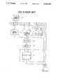
- FIG. 2is a block diagram of a first conventional signal processing circuit
- FIG. 3is a block diagram of a second conventional signal processing circuit
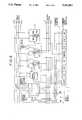
- FIG. 4is a block diagram of a signal processing circuit in a first preferred embodiment according to the invention.
- FIG. 5is a block diagram of an arithmetic block of the signal processing circuit in the first preferred embodiment according to the invention.
- FIG. 6is a block diagram of an arithmetic block of a signal processing circuit in a second preferred embodiment according to the invention.
- FIGS. 1A to 1Cshow butterfly arithmetic process in the FCT process.
- FIG. 2shows the first conventional signal processing circuit.
- the signal processing circuitincludes a data memory 4 for storing pixel data of picture flames connected with a data bus 16, a program memory 11 for storing programs connected with a data bus 15, a register 9 connected with the data bus 16, a selecting circuit 12 which selectively supplies an output signal from data of the data buses 15 and 16, a multiplier 5 which multiplies the data of the data bus 16 by the output of the selecting circuit 12, a shift register 6 which shifts the output of the multiplier 5, a selecting circuit 13 which selectively supplies an output signal from the output of the shift register 6 and an accumulator 8 which will be mentioned after, an arithmetic circuit (an arithmetic logic unit) 7 which carries out arithmetic operation of an output of the selecting circuit 13 and an output of the accumulator 8, the accumulator 8 which accumulates an output of the arithmetic circuit 7 and supplies an output signal to the data bus 16, a register 9 which temporally stores data of the data bus 16, a selecting circuit 14 which selective
- FIG. 3shows the second conventional signal processing circuit.
- the signal processing circuitincludes a data memory 4 connected with data buses X and Y of data bus 19, an arithmetic circuit 7 which carries out arithmetic operation of the data of the data buses X and Y, and a multiplier 5 which multiplies a first input signal from the buses X and Y and an output of the arithmetic circuit 7 by a second input signal from the bus X and the output of the arithmetic circuit 7 a barrel shifter 17 connected to the buses X and Y, a register 9 supplied with a signal from the multiplier 5, the arithmetic circuit 7 and the barrel shifter 17, a shifter 18 having an input connected to an output of the register 9 and an output connected to a bus Z of the bus 19, and an accumulator 8 having a first input connected to the output of the shifter 18, and a second input connected to one of three output, the remaining two outputs of which are connected to the buses X and Y.
- the signal processing circuitincludes a instruction memory 1 for storing instructions of the program, a instruction decoder 2 which decodes the instructions supplied from the instruction memory 1, an arithmetic block 3 which carries out arithmetic process in accordance with the instruction supplied from the instruction decoder 2, and a data memory 4 for storing data.
- FIG. 5shows a detail block structure of the arithmetic block 3 of the signal processing circuit shown in FIG. 4.
- the arithmetic block 3includes a general-purpose register 31 of multi-port type including a plurality of registers, an address decoder 32, an arithmetic logic unit 33, a multiplying and accumulating unit 34, input paths 35 and 36 from the register 31 to the units 33 and 34, and output paths 37 and 38 from the units 33 and 34 to the register 31.
- a instructionis read from the instruction memory 1 and decoded by the instruction decoder 2 to be supplied to the arithmetic block 3.
- dataare read from the data memory 4 through an output path MO of the data memory 4 to be stored to the general-purpose register 31.
- Each datais stored in a corresponding register of the general-purpose register in accordance with a corresponding address designated by the address decoder 32.
- the dataare transmitted to the arithmetic unit 33 and the multiplying and accumulating unit 34 through the input paths 35 and 36 respectively to carry out predetermined arithmetic processes which are ordered by the instruction.
- the results of the arithmetic Processare transferred from the arithmetic unit 33 and the multiplying and accumulating unit 34 to the general-purpose register 31 through the output paths 37 and 38 respectively, and then written to the data memory 4 through an input path MI of the data memory 4.
- the basic structure of the signal processing circuit in the second preferred embodimentis the same as that of the signal processing circuit in the first preferred embodiment, however, the structure of an arithmetic block thereof is explained in more detail in compared with that in the first preferred embodiment.
- the arithmetic block thereofincludes a general-purpose register 41 of multi-port type, an address decoder 42, an arithmetic unit 43 including a barrel shifter 44 and two arithmetic circuits (two arithmetic logic units) 45 and 46, and a multiplying and accumulating unit 47.
- the general-purpose register 41includes a plurality of single registers.
- the general-purpose register 41is connected with the data memory 4 by input and output paths MI and MO through which data are read therefrom and written thereto.
- the general-purpose register 41is connected with input paths 48 to 51 and output paths 52 to 54 through which the data are transferred from the general-purpose register 41 to the arithmetic unit 43 and the multiplying and accumulating unit 47.
- the address decoder 42designates an address of a corresponding single register of the general-purpose register 41 in accordance with instructions stored in a instruction decode register 21 of the instruction decoder 2.
- instruction stored in the instruction memory 1are read therefrom to the instruction decoder 2.
- the instructionsare decoded and stored in the instruction decode register 21 in the instruction decoder 2.
- the instructionsare transferred to the address decoder 42, the barrel shifter 44, the arithmetic circuits 45 and 46, and the multiplying and accumulating unit 47 in accordance with fields of the decoder register 21 to which the instructions belong.
- necessary data for arithmetic processare transferred from the data memory 4 to the general-purpose register 41 through the input path MI, and then transferred to the barrel shifter 44 and the arithmetic circuits 45 and 46 through the input paths 48 and 49 and to the multiplying and accumulating unit 47 through the input paths 50 and 51, and then predetermined arithmetic processes are carried out at each of the barrel shifter 44, the arithmetic circuits 45 and 46, and the multiplying and accumulating unit 47.
- the results of the arithmetic processesare transferred to the general-purpose register 41 from the barrel shifter 44 through the output path 52, from the arithmetic circuits 45 and 46 through the output paths 52 and 54, and from the multiplying and accumulating unit 47 through the output paths 53 and 54, and then transmitted to the data memory 4 through the output path MO.
- the DCT process ⁇ X j Y kwill be explained.
- data X j and Y kare loaded from the data memory 4 to a register pair (sr1' and sr2') of the general-purpose register 41.
- the data X j and Y kare transferred to the multiplying and accumulating unit 47, in which multiplication of X j and Y k is carried out and the product of X j and Y k is accumulated.
- the result of the DCT process ⁇ X j Y kcan be obtained by carrying out the first and second steps repeatedly.
- the inner and inter frame adaptation forecast processed ⁇ (X j -Y k ) 2will be explained.
- data X j and Y kare loaded from the data memory 4 to a register pair (sr1 and sr2) of the general-purpose register 41.
- the data X j and Y kare transferred to the arithmetic circuit 45, and arithmetic process of (X j -Y k ) is carried out.
- the resultis stored as a first arithmetic data in a register (dst) of the general-purpose register 41.
- the first arithmetic datais transferred to the multiplying and accumulating unit 47, and accumulation process is carried out.
- the result of the inner and inter frame adaptation forecast process ⁇ (X j -Y k ) 2can be obtained by carrying out the first to third steps repeatedly.
- data (a) and (x)are loaded to a register pair (sr1' and sr2') of the general-purpose register 41 from the data memory 4.
- the data (a) and (x)are transferred to the multiplying and accumulating unit 47, in which multiplication of (a) and (x) is carried out, and the product (a ⁇ x) is stored in a register (dst') of the general-purpose register 41.
- data (y)is loaded to a register (sr2') of the general-purpose register 41 from the data memory 4.
- the data (a) and (y)are transferred to the multiplying and accumulating unit 47, in which multiplication of (a) and (y) is carried out, and the product (a ⁇ y) is stored in a register (dst") of the general-purpose register 41.
- arithmetic process of (a ⁇ x+a ⁇ y)is carried out at the arithmetic circuit 45, and the result is stored in a register (dst) of the general-purpose register 41.
- arithmetic process of (a ⁇ x-a ⁇ y)is carried out at the arithmetic circuit 46, and the result is stored in a register (dst) of the general-purpose register 41.
- arithmetic processes in the arithmetic circuit and loading and accessing of data from the data memoryare carried out in parallel by one instruction. Further, it is not necessary to rewrite the processed data in each time after arithmetic process in the FCT process, so that there is required smaller number of steps.
Landscapes
- Engineering & Computer Science (AREA)
- General Physics & Mathematics (AREA)
- Theoretical Computer Science (AREA)
- Physics & Mathematics (AREA)
- Mathematical Optimization (AREA)
- Mathematical Analysis (AREA)
- Pure & Applied Mathematics (AREA)
- General Engineering & Computer Science (AREA)
- Computational Mathematics (AREA)
- Software Systems (AREA)
- Computing Systems (AREA)
- Complex Calculations (AREA)
- Compression Or Coding Systems Of Tv Signals (AREA)
- Advance Control (AREA)
- Image Processing (AREA)
Abstract
Description
Σ|X.sub.j -Y.sub.k | (1)
ΣX.sub.j Y.sub.k ( 2)
Σ(X.sub.j -Y.sub.k).sup.2 ( 3)
Claims (4)
Applications Claiming Priority (2)
| Application Number | Priority Date | Filing Date | Title |
|---|---|---|---|
| JP29608090AJP2959104B2 (en) | 1990-10-31 | 1990-10-31 | Signal processor |
| JP2-296080 | 1990-10-31 |
Publications (1)
| Publication Number | Publication Date |
|---|---|
| US5260897Atrue US5260897A (en) | 1993-11-09 |
Family
ID=17828862
Family Applications (1)
| Application Number | Title | Priority Date | Filing Date |
|---|---|---|---|
| US07/783,907Expired - LifetimeUS5260897A (en) | 1990-10-31 | 1991-10-29 | Signal processing circuit |
Country Status (3)
| Country | Link |
|---|---|
| US (1) | US5260897A (en) |
| EP (1) | EP0483861A3 (en) |
| JP (1) | JP2959104B2 (en) |
Cited By (15)
| Publication number | Priority date | Publication date | Assignee | Title |
|---|---|---|---|---|
| US5517436A (en)* | 1994-06-07 | 1996-05-14 | Andreas; David C. | Digital signal processor for audio applications |
| US5532938A (en)* | 1994-01-28 | 1996-07-02 | Mitsubishi Denki Kabushiki Kaisha | Numerical arithmetic processing unit |
| US5594679A (en)* | 1993-03-31 | 1997-01-14 | Sony Corporation | Adaptive video signal processing apparatus |
| US5636150A (en)* | 1992-08-06 | 1997-06-03 | Sharp Kabushiki Kaisha | Data driven type digital filter unit and data driven type information processor including the same |
| US5740092A (en)* | 1993-09-02 | 1998-04-14 | Matsushita Electric Industrial Co., Ltd. | Signal processor |
| US5904731A (en)* | 1994-07-28 | 1999-05-18 | Fujitsu Limited | Product-sum device suitable for IIR and FIR operations |
| US6092179A (en)* | 1991-02-05 | 2000-07-18 | Lucent Technologies Inc. | Core processor with customizable function unit |
| US6205459B1 (en)* | 1996-12-18 | 2001-03-20 | Yamaha Corporation | Digital signal processor and digital signal processing system incorporating same |
| US6240437B1 (en)* | 1993-11-30 | 2001-05-29 | Texas Instruments Incorporated | Long instruction word controlling plural independent processor operations |
| US6247036B1 (en)* | 1996-01-22 | 2001-06-12 | Infinite Technology Corp. | Processor with reconfigurable arithmetic data path |
| US6260136B1 (en)* | 1997-08-20 | 2001-07-10 | Matsushita Electric Industrial Co., Ltd. | Substitute register for use in a high speed data processor |
| US6298364B1 (en)* | 1993-03-08 | 2001-10-02 | Sharp Kabushiki Kaisha | Digital signal processing operation apparatus that allows combined operation |
| US6317770B1 (en)* | 1997-08-30 | 2001-11-13 | Lg Electronics Inc. | High speed digital signal processor |
| US20100299471A1 (en)* | 2003-07-30 | 2010-11-25 | Pankaj Shrivastava | Microcontroller with an Interrupt Structure Having Programmable Priority Levels with each Priority Level Associated with a Different Register Set |
| US8589464B1 (en)* | 2003-01-10 | 2013-11-19 | Altera Corporation | Arithmetic logic unit |
Families Citing this family (6)
| Publication number | Priority date | Publication date | Assignee | Title |
|---|---|---|---|---|
| US6370623B1 (en) | 1988-12-28 | 2002-04-09 | Philips Electronics North America Corporation | Multiport register file to accommodate data of differing lengths |
| US6058473A (en)* | 1993-11-30 | 2000-05-02 | Texas Instruments Incorporated | Memory store from a register pair conditional upon a selected status bit |
| JPH07248918A (en)* | 1994-03-10 | 1995-09-26 | Matsushita Electric Ind Co Ltd | Microprocessor |
| US5600674A (en)* | 1995-03-02 | 1997-02-04 | Motorola Inc. | Method and apparatus of an enhanced digital signal processor |
| TW439380B (en) | 1995-10-09 | 2001-06-07 | Hitachi Ltd | Terminal apparatus |
| JPH1063500A (en)* | 1996-08-23 | 1998-03-06 | Matsushita Electric Ind Co Ltd | Signal processing device |
Citations (7)
| Publication number | Priority date | Publication date | Assignee | Title |
|---|---|---|---|---|
| US4825359A (en)* | 1983-01-18 | 1989-04-25 | Mitsubishi Denki Kabushiki Kaisha | Data processing system for array computation |
| US4852048A (en)* | 1985-12-12 | 1989-07-25 | Itt Corporation | Single instruction multiple data (SIMD) cellular array processing apparatus employing a common bus where a first number of bits manifest a first bus portion and a second number of bits manifest a second bus portion |
| US4901267A (en)* | 1988-03-14 | 1990-02-13 | Weitek Corporation | Floating point circuit with configurable number of multiplier cycles and variable divide cycle ratio |
| US4996661A (en)* | 1988-10-05 | 1991-02-26 | United Technologies Corporation | Single chip complex floating point numeric processor |
| US5113523A (en)* | 1985-05-06 | 1992-05-12 | Ncube Corporation | High performance computer system |
| US5129092A (en)* | 1987-06-01 | 1992-07-07 | Applied Intelligent Systems,Inc. | Linear chain of parallel processors and method of using same |
| US5136717A (en)* | 1988-11-23 | 1992-08-04 | Flavors Technology Inc. | Realtime systolic, multiple-instruction, single-data parallel computer system |
Family Cites Families (2)
| Publication number | Priority date | Publication date | Assignee | Title |
|---|---|---|---|---|
| IT991096B (en)* | 1973-07-10 | 1975-07-30 | Honeywell Inf Systems | ELECTRONIC CALCULATOR WITH INDEPENDENT FUNCTIONAL NETWORKS FOR THE SIMULTANEOUS EXECUTION OF DIFFERENT OPERATIONS ON THE SAME DATA |
| US5175863A (en)* | 1989-10-23 | 1992-12-29 | International Business Machines Corporation | Signal data processing system having independently, simultaneously operable alu and macu |
- 1990
- 1990-10-31JPJP29608090Apatent/JP2959104B2/ennot_activeExpired - Fee Related
- 1991
- 1991-10-29USUS07/783,907patent/US5260897A/ennot_activeExpired - Lifetime
- 1991-10-31EPEP19910118640patent/EP0483861A3/ennot_activeWithdrawn
Patent Citations (7)
| Publication number | Priority date | Publication date | Assignee | Title |
|---|---|---|---|---|
| US4825359A (en)* | 1983-01-18 | 1989-04-25 | Mitsubishi Denki Kabushiki Kaisha | Data processing system for array computation |
| US5113523A (en)* | 1985-05-06 | 1992-05-12 | Ncube Corporation | High performance computer system |
| US4852048A (en)* | 1985-12-12 | 1989-07-25 | Itt Corporation | Single instruction multiple data (SIMD) cellular array processing apparatus employing a common bus where a first number of bits manifest a first bus portion and a second number of bits manifest a second bus portion |
| US5129092A (en)* | 1987-06-01 | 1992-07-07 | Applied Intelligent Systems,Inc. | Linear chain of parallel processors and method of using same |
| US4901267A (en)* | 1988-03-14 | 1990-02-13 | Weitek Corporation | Floating point circuit with configurable number of multiplier cycles and variable divide cycle ratio |
| US4996661A (en)* | 1988-10-05 | 1991-02-26 | United Technologies Corporation | Single chip complex floating point numeric processor |
| US5136717A (en)* | 1988-11-23 | 1992-08-04 | Flavors Technology Inc. | Realtime systolic, multiple-instruction, single-data parallel computer system |
Cited By (17)
| Publication number | Priority date | Publication date | Assignee | Title |
|---|---|---|---|---|
| US6092179A (en)* | 1991-02-05 | 2000-07-18 | Lucent Technologies Inc. | Core processor with customizable function unit |
| US5636150A (en)* | 1992-08-06 | 1997-06-03 | Sharp Kabushiki Kaisha | Data driven type digital filter unit and data driven type information processor including the same |
| US6298364B1 (en)* | 1993-03-08 | 2001-10-02 | Sharp Kabushiki Kaisha | Digital signal processing operation apparatus that allows combined operation |
| US5594679A (en)* | 1993-03-31 | 1997-01-14 | Sony Corporation | Adaptive video signal processing apparatus |
| US5740092A (en)* | 1993-09-02 | 1998-04-14 | Matsushita Electric Industrial Co., Ltd. | Signal processor |
| US6240437B1 (en)* | 1993-11-30 | 2001-05-29 | Texas Instruments Incorporated | Long instruction word controlling plural independent processor operations |
| US5532938A (en)* | 1994-01-28 | 1996-07-02 | Mitsubishi Denki Kabushiki Kaisha | Numerical arithmetic processing unit |
| US5517436A (en)* | 1994-06-07 | 1996-05-14 | Andreas; David C. | Digital signal processor for audio applications |
| US5904731A (en)* | 1994-07-28 | 1999-05-18 | Fujitsu Limited | Product-sum device suitable for IIR and FIR operations |
| US6247036B1 (en)* | 1996-01-22 | 2001-06-12 | Infinite Technology Corp. | Processor with reconfigurable arithmetic data path |
| US6205459B1 (en)* | 1996-12-18 | 2001-03-20 | Yamaha Corporation | Digital signal processor and digital signal processing system incorporating same |
| US6260136B1 (en)* | 1997-08-20 | 2001-07-10 | Matsushita Electric Industrial Co., Ltd. | Substitute register for use in a high speed data processor |
| US6317770B1 (en)* | 1997-08-30 | 2001-11-13 | Lg Electronics Inc. | High speed digital signal processor |
| US6463451B2 (en) | 1997-08-30 | 2002-10-08 | Lg Electronics Inc. | High speed digital signal processor |
| US8589464B1 (en)* | 2003-01-10 | 2013-11-19 | Altera Corporation | Arithmetic logic unit |
| US20100299471A1 (en)* | 2003-07-30 | 2010-11-25 | Pankaj Shrivastava | Microcontroller with an Interrupt Structure Having Programmable Priority Levels with each Priority Level Associated with a Different Register Set |
| US8392641B2 (en)* | 2003-07-30 | 2013-03-05 | Nxp B.V. | Microcontroller with an interrupt structure having programmable priority levels with each priority level associated with a different register set |
Also Published As
| Publication number | Publication date |
|---|---|
| EP0483861A2 (en) | 1992-05-06 |
| JPH04167168A (en) | 1992-06-15 |
| EP0483861A3 (en) | 1993-06-02 |
| JP2959104B2 (en) | 1999-10-06 |
Similar Documents
| Publication | Publication Date | Title |
|---|---|---|
| US5260897A (en) | Signal processing circuit | |
| US5901248A (en) | Programmable architecture and methods for motion estimation | |
| US6421698B1 (en) | Multipurpose processor for motion estimation, pixel processing, and general processing | |
| US5268853A (en) | Orthogonal transformation processor for compressing information | |
| US20010046264A1 (en) | Programmable architecture and methods for motion estimation | |
| US20040062308A1 (en) | System and method for accelerating video data processing | |
| JP3526976B2 (en) | Processor and data processing device | |
| JP3442192B2 (en) | Data-driven information processor | |
| WO1988009016A1 (en) | Vector processor for processing recurrent equations at a high speed | |
| EP0762328B1 (en) | Image processing device | |
| JPS61241877A (en) | Space product sum arithmetic unit | |
| US4853887A (en) | Binary adder having a fixed operand and parallel-serial binary multiplier incorporating such an adder | |
| US5363322A (en) | Data processor with an integer multiplication function on a fractional multiplier | |
| NO169989B (en) | VECTOR MANAGEMENT SYSTEM | |
| US6160850A (en) | Motion estimator employing a three-step hierachical search block-matching algorithm | |
| EP1691334A1 (en) | Method for encoding co-ordinates of a video image moving along the display of a computing device | |
| US5029018A (en) | Structure of image processing system | |
| US5477469A (en) | Operation device and operation method for discrete cosine transform and inverse discrete cosine transform | |
| US5886912A (en) | Processing elements connected in cascade having a controllable bypass | |
| US5359549A (en) | Orthogonal transformation processor for compressing information | |
| US5379076A (en) | Video motion compensation circuit | |
| JPH07152730A (en) | Discrete cosine transform device | |
| JP3305406B2 (en) | Program-controlled processor | |
| JP2960328B2 (en) | Apparatus for providing operands to "n + 1" operators located in a systolic architecture | |
| US7555513B2 (en) | SIMD processor having enhanced operand storage interconnects |
Legal Events
| Date | Code | Title | Description |
|---|---|---|---|
| AS | Assignment | Owner name:NEC CORPORATION, JAPAN Free format text:ASSIGNMENT OF ASSIGNORS INTEREST.;ASSIGNORS:TORIUMI, YOSHITAKA;YOSHIDA, AKIO;REEL/FRAME:005898/0737 Effective date:19911028 | |
| STCF | Information on status: patent grant | Free format text:PATENTED CASE | |
| FEPP | Fee payment procedure | Free format text:PAYOR NUMBER ASSIGNED (ORIGINAL EVENT CODE: ASPN); ENTITY STATUS OF PATENT OWNER: LARGE ENTITY | |
| FPAY | Fee payment | Year of fee payment:4 | |
| FEPP | Fee payment procedure | Free format text:PAYER NUMBER DE-ASSIGNED (ORIGINAL EVENT CODE: RMPN); ENTITY STATUS OF PATENT OWNER: LARGE ENTITY Free format text:PAYOR NUMBER ASSIGNED (ORIGINAL EVENT CODE: ASPN); ENTITY STATUS OF PATENT OWNER: LARGE ENTITY | |
| FPAY | Fee payment | Year of fee payment:8 | |
| AS | Assignment | Owner name:NEC ELECTRONICS CORPORATION, JAPAN Free format text:ASSIGNMENT OF ASSIGNORS INTEREST;ASSIGNOR:NEC CORPORATION;REEL/FRAME:013758/0440 Effective date:20021101 | |
| FPAY | Fee payment | Year of fee payment:12 |