US5260718A - Liquid crystal shutter xerographic printer with offset configuration lamp aperture and copier/printer with optically aligned lamps, image bars, and lenses - Google Patents
Liquid crystal shutter xerographic printer with offset configuration lamp aperture and copier/printer with optically aligned lamps, image bars, and lensesDownload PDFInfo
- Publication number
- US5260718A US5260718AUS07/816,782US81678292AUS5260718AUS 5260718 AUS5260718 AUS 5260718AUS 81678292 AUS81678292 AUS 81678292AUS 5260718 AUS5260718 AUS 5260718A
- Authority
- US
- United States
- Prior art keywords
- image
- bars
- printer
- bar
- liquid crystal
- Prior art date
- Legal status (The legal status is an assumption and is not a legal conclusion. Google has not performed a legal analysis and makes no representation as to the accuracy of the status listed.)
- Expired - Fee Related
Links
Images


Classifications
- G—PHYSICS
- G06—COMPUTING OR CALCULATING; COUNTING
- G06K—GRAPHICAL DATA READING; PRESENTATION OF DATA; RECORD CARRIERS; HANDLING RECORD CARRIERS
- G06K15/00—Arrangements for producing a permanent visual presentation of the output data, e.g. computer output printers
- G06K15/02—Arrangements for producing a permanent visual presentation of the output data, e.g. computer output printers using printers
- G06K15/12—Arrangements for producing a permanent visual presentation of the output data, e.g. computer output printers using printers by photographic printing, e.g. by laser printers
- G06K15/1238—Arrangements for producing a permanent visual presentation of the output data, e.g. computer output printers using printers by photographic printing, e.g. by laser printers simultaneously exposing more than one point
- G06K15/1242—Arrangements for producing a permanent visual presentation of the output data, e.g. computer output printers using printers by photographic printing, e.g. by laser printers simultaneously exposing more than one point on one main scanning line
- B—PERFORMING OPERATIONS; TRANSPORTING
- B41—PRINTING; LINING MACHINES; TYPEWRITERS; STAMPS
- B41J—TYPEWRITERS; SELECTIVE PRINTING MECHANISMS, i.e. MECHANISMS PRINTING OTHERWISE THAN FROM A FORME; CORRECTION OF TYPOGRAPHICAL ERRORS
- B41J2/00—Typewriters or selective printing mechanisms characterised by the printing or marking process for which they are designed
- B41J2/435—Typewriters or selective printing mechanisms characterised by the printing or marking process for which they are designed characterised by selective application of radiation to a printing material or impression-transfer material
- B41J2/465—Typewriters or selective printing mechanisms characterised by the printing or marking process for which they are designed characterised by selective application of radiation to a printing material or impression-transfer material using masks, e.g. light-switching masks
- G—PHYSICS
- G03—PHOTOGRAPHY; CINEMATOGRAPHY; ANALOGOUS TECHNIQUES USING WAVES OTHER THAN OPTICAL WAVES; ELECTROGRAPHY; HOLOGRAPHY
- G03G—ELECTROGRAPHY; ELECTROPHOTOGRAPHY; MAGNETOGRAPHY
- G03G15/00—Apparatus for electrographic processes using a charge pattern
- G03G15/04—Apparatus for electrographic processes using a charge pattern for exposing, i.e. imagewise exposure by optically projecting the original image on a photoconductive recording material
- G03G15/04036—Details of illuminating systems, e.g. lamps, reflectors
- G03G15/04045—Details of illuminating systems, e.g. lamps, reflectors for exposing image information provided otherwise than by directly projecting the original image onto the photoconductive recording material, e.g. digital copiers
- G—PHYSICS
- G03—PHOTOGRAPHY; CINEMATOGRAPHY; ANALOGOUS TECHNIQUES USING WAVES OTHER THAN OPTICAL WAVES; ELECTROGRAPHY; HOLOGRAPHY
- G03G—ELECTROGRAPHY; ELECTROPHOTOGRAPHY; MAGNETOGRAPHY
- G03G15/00—Apparatus for electrographic processes using a charge pattern
- G03G15/22—Apparatus for electrographic processes using a charge pattern involving the combination of more than one step according to groups G03G13/02 - G03G13/20
- G03G15/221—Machines other than electrographic copiers, e.g. electrophotographic cameras, electrostatic typewriters
- H—ELECTRICITY
- H04—ELECTRIC COMMUNICATION TECHNIQUE
- H04N—PICTORIAL COMMUNICATION, e.g. TELEVISION
- H04N1/00—Scanning, transmission or reproduction of documents or the like, e.g. facsimile transmission; Details thereof
- H04N1/04—Scanning arrangements, i.e. arrangements for the displacement of active reading or reproducing elements relative to the original or reproducing medium, or vice versa
- H04N1/19—Scanning arrangements, i.e. arrangements for the displacement of active reading or reproducing elements relative to the original or reproducing medium, or vice versa using multi-element arrays
- H04N1/191—Scanning arrangements, i.e. arrangements for the displacement of active reading or reproducing elements relative to the original or reproducing medium, or vice versa using multi-element arrays the array comprising a one-dimensional array, or a combination of one-dimensional arrays, or a substantially one-dimensional array, e.g. an array of staggered elements
- H04N1/192—Simultaneously or substantially simultaneously scanning picture elements on one main scanning line
- H04N1/193—Simultaneously or substantially simultaneously scanning picture elements on one main scanning line using electrically scanned linear arrays, e.g. linear CCD arrays
Definitions
- the present inventionrelates to an electrophotographic printer utilizing an addressable image bar as the imaging device, and, more particularly, to a printer which utilizes a plurality of addressable image bars arranged generally linearly in an alternately staggered orientation.
- U.S. Pat. No. 4,386,836discloses a printer in which a "optical writing unit" in conjunction with an imaging lens forms a latent image on a photoreceptor surface.
- the "optical writing unit”includes a light source which illuminates a liquid crystal shutter apparatus. Depending on the transmissivity of the individual shutters (which is set by a prescribed data input signal), light that passes through the shutter exposes the photoreceptor.
- U.S. Pat. No. 4,595,259describes another printing system which includes a liquid crystal image bar which selectively transmits light into a lens so as to form latent electrostatic images a line at a time on a photoreceptor surface.
- the lensmay be a conventional lens or a linear lens such as a SelfocTM lens array.
- U.S. Pat. No. 4,728,972discloses the exposure of a xerographic drum through a liquid crystal bar controlled by a multiplexing driving circuit.
- image barused in electrophotographic printers is disclosed, for example, in U.S. Pat. No. 4,477,175.
- image barcomprises a plurality of individually activated light emitting diodes (LEDs).
- the image bars disclosed in the above patents and publicationsare linear substrates having an effective length equivalent to the width of the standard letter size document, e.g. 81/2 inches.
- the longer the image bar lengththe greater the difficulty of manufacturing and the greater the cost. The reason for this is that the yield of these bars decreases exponentially with increased pixel density in active areas in a linear direction.
- an image bar of effectively increased lengthis realized when a plurality of image bars linearly aligned in a staggered orientation are optically aligned with their outputs focused to a common line at a photoreceptor.
- the barsare displaced from each other in a direction perpendicular to the process direction of the moving photoreceptor.
- This concept of staggering shorter image bars to effectively form a bar of longer lengthenables a second aspect of the invention: the ability to print documents of a much greater width than the current letter size.
- engineering drawings with widths up to 36 inchescan be formed by a plurality of bars arranged according to the teachings of the invention.
- a multifunction copier/printeris enabled by creating an architecture whereby the image bars are positioned so as to permit an additional imaging path to be established therebetween. This arrangement makes possible a machine which conventionally copies documents placed on a platen as well as printing documents electronically.
- the present inventionis directed toward an electrophotographic printer for line by line exposure of a moving photoreceptor surface, and includes an imaging system comprising a plurality of image bars aligned linearly in two parallel rows, a pair of linear lens arrays positioned between said image bars and said photoreceptor surface, each lens array optically aligned with one of said image bar rows, said lens array being tilted with respect to one another, and means for selectively addressing said image bars to create a modulated light output whereby said lens arrays transmit the output of the image bars in each row to a common focus line at the photoreceptor surface.
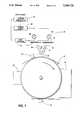
- FIG. 1shows a side view of an imaging system for an electrophotographic printer incorporating the staggered liquid crystal image bar assembly according to the present invention.
- FIG. 2is a top view of the FIG. 1 system.
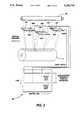
- FIG. 3is a side perspective view of the imaging system of FIG. 1 together with a representation of the data flow to the image bars
- FIG. 4is a schematic representation of the drive circuit of an image bar.
- FIG. 5is a block diagram of the data flow control circuits for the image bar.
- FIGS. 6A, 6B, and 6Care schematic representations of three butting configurations possible with three adjacent image bars.
- FIG. 7is a side view of a copier/printer incorporating two liquid crystal image bar assemblies to enable the print function and a conventional optical assembly to enable the function of copying a document on a document platen
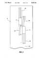
- FIG. 8is a bottom view of the illuminator source for the image bar showing an aperture which complements the offset structure of the underlying image bars.
- an electrophotographic printer 10utilizing an image bar assembly constructed according the principles of the present invention and arranged in a horizontal plane.
- the printer 10includes a series of process stations through which a photoreceptor drum 14 passes beginning with the image station 15 where the latent electrostatic image is formed.
- Drum 14moves past development station 16, transfer station 18, cleaning station 20, and corona charging station 22.
- a pair of illumination sources 28, 29which in a preferred embodiment are T12 apertured fluorescent lamps, are energized by high frequency power supply 30 under control of system controller 32. Lamps 28, 29 illuminate assemblies 12 and 13, respectively.
- Bar assembly 12contains two liquid crystal image bars 12A, 12C; (FIG. 2) bar assembly 13 contains two liquid crystal image bars 13B, 13D. As shown in FIG. 2, the image bars are arranged to form linear arrays with each image bar being offset or staggered from the others. Each image bar has two offset rows of linear liquid crystal pixels. The transmissive state of each image bar is determined by selective application of a voltage to a plurality of electrodes on the image bar substrate. Bar control circuit 33 energizes the appropriate electrodes in response to digitized bit-mapped data input representing document information typically sent from a charge coupled device or from a computer and stored in controller memory. Bar control circuitry 33 is discussed in further detail below.
- Each bit of datais polarized ("1" or "0") to indicate whether the picture elements "pixels" it represents is to be printed black or white.
- image bars 12A, 13B, 12C, 13Dselectively pass light to a pair of linear gradient index lens arrays 40, 42, which in a preferred embodiment are SelfocTM SLA 12 lenses manufactured by Nippon Sheet Glass Company.
- the lensesimage the light outputs (as two linear arrays of dots) from the staggered arrays as two lines at the photoreceptor surface.
- the space between the lensesis filled with an opaque spacer 43. With conventional lenses, such a tilted field would produce unacceptable image degradation at the photoreceptor, but the properties of gradient index lenses, which form an erect image, result in much less distortion.
- a method of registering the image bar in the process and scan directionis presented so as to ensure proper overlap at the ends of the bar to accommodate the required "stitching" of the several focused bar images.
- FIG. 3there is shown a side prospective view of FIG. 1 showing three of the bars (12A, 13B, 12C) beneath lamp 28.
- the SelfocTM lens arrayshave been omitted for clarity of description.
- the registration problems to be solvedare: (1) to register each of the bars in the process direction so that the portions of the scan line projected from bar 13B align with the correct positions of scan lines projected from bars 12A and 12C, and (2) to register the bars in the scan direction to ensure that projected pixels do not overlap or leave a gap. As shown in FIG.
- the raster formatted input datais recovered and stored in data buffer 46, located in bar control 33 as shown, and then read out in proper sequence to the three bars. It is evident that the data must be divided into three columns and directed to each of the three bars. Since the bars are multiplexed, i.e., each possesses two offset rows 50, 52 of pixels, with both energized at the same time. Since these odd and even rows are offset, the data supplied must be similarly offset. In order to obtain this offset, the data is read out of memory displaced by this offset, as shown.
- FIG. 4is the functional representation of one of the image bars (12A) and associated driving circuit. As shown, there are two rows of pixels 50A, 52A (odd and even), of which one is active, based on the voltage applied by a backplane driver circuit 54. Each pixel driver thus services two adjacent pixels in this 2:1 multiplexing approach. The offset (in the process direction) between the rows of odd and even pixels gives rise to the different loci in the data buffer 46 (FIG. 3) from which odd bits and even bits are alternately selected. The system is block-diagrammed in FIG. 5. Referring to FIGS. 4 and 5, there is within bar controller 32 a binary counter 60, whose outputs select different locations in ROM 62.
- Each ROM locusholds a value which is an address in RAM 64 at which words of the incoming scan line will be stored, or from which words will be selected as their bits are dumped to the image bar.
- the sequence of operationis as follows: (1) data to be written into RAM 64 is presented to the RAM data input. The location of the address where these data are to be stored is located in ROM 62 and presented to the RAM. A R/W signal from bar control 33 signals the RAM to write the data. (2) The controller increments counter 60 so that ROM 64 now outputs the address of the data to be dumped into the first top register of shift register circuit 70. On the first half cycle, only the odd bits are chosen by a selection circuit 72. These data follow the data path to the shift register.
- Control 33increments counter 60 and suitably selected data are sent to the second shift register. (4) Then another 16 bits of data are written into RAM 64. (5) The third and fourth shift registers are loaded while the first and second shift registers are clocked out. (6) More data are written into RAM. (7) The fifth and sixth shift registers are loaded while one through four are being shifted out. (8) The sequence continues until all the odd bits of one line are in the correct position in the image bars; then they are latched by latching circuit 78 (FIG. 4). (9) The selector 72 shifts to choose the even bits, which are then sent to the shift registers in the image bars while the odd bits are printing.
- FIG. 6The problem of registration in the scan direction is illustrated in FIG. 6, where, in the top sketch, FIG. 6A, bars 12A, 13B, 12C are perfectly butted with neither overlap nor gap present.
- the center sketch, FIG. 6Bassumes a one-pixel overlap on each end, where bars 12A and 12C each overlap bar 13B by one pixel. Although equal overlaps are shown, the present invention allows independent correction for overlap of bars 12A and 12C with bar 13B.
- Shift registers 70(FIG. 4) serially shift the video data in the direction indicated by the two arrows on each bar.
- a scan lineconsists of 14,592 bits, numbered 0 through 14,591. Each image bar is illuminated from above by a fluorescent lamps 28, 29 as shown in FIG. 1.
- each baris projected down onto the drum 12 as shown in FIG. 3. Since the bars have two rows of pixels at the imaging plane, the drum surface sees alternately a row of odd pixel data followed by a row of even pixel data (which rows are displaced in time based on process speed and inter-row spacing on the bars). Although the ends of the rows of imaged pixels can in principle be juxtaposed at the drum surface via projection optics, adjacent bars cannot be butted (because edge-sealing requirement for the bar occupy some minimum width, typically 1/16 inch).
- the second shift register feeding that portion of bar 12A closest to the overlapmust fill in the final bit(s) with "dark" data so as not to "overwrite” bits of bar 13B.
- bar 12C's datamust be shifted fewer clocks with increasing overlap (the first bit lost is 0, then 1, etc.).
- scan line bit 4863 (bar 12C)will always image next to bit 4864 (bar 13B).
- the shift registermust first shift in dark data, which are simply shifted off the end in the case of no-overlap positioning.
- Another concern which must be addressedis that, since each shift register handles an integral number of 16-bit words, as overlapping occurs the first bits which would normally be shifted into the second register must be shifted last into the first register.
- the last bits which would normally be shifted into the fifth registermust be shifted first into the 6th bar register.
- This processis further complicated by the fact that, for odd-bit overlaps of bar 12A, an odd bit jumps the SR 1/SR2 boundary, but an even bit doesn't.
- an even bitjumps the SR5/SR6 boundary, but an odd bit doesn't.
- the final concernis that the odd/even polarity of the bits is, for odd bit overlaps, different from that for even bit overlaps. Referring again to FIG. 6, note that in the top and bottom panels (zero and two bit overlaps, respectively), the odd bits are in the top row for all three bars.
- the RAM 64(FIG. 5) is filled with incoming scan line video data, and simultaneously dumped to the bars based on the overlap(s) and the process direction displacement of bar 13B with respect to bars 12A, 12C.
- the addresses in RAM for fill and dumpare contained in ROM 62; switches select different ROM areas (and hence different RAM addresses) for different process-direction displacements. Other switches determine the amount by which the video data is advanced in the scan direction (for bar 12B) or delayed in the scan direction (for 12C) based on the respective overlaps.
- the liquid crystal image baris a transient nematic liquid crystal driven by a single frequency voltage source.
- the liquid crystal deviceis disclosed in U.S. Pat. No. 4,595,259 and an improvement thereto is disclosed in U.S. Pat. No. 4,767,190. These patents describe the construction and operating parameters suitable for the present liquid crystal array and their contents are hereby incorporated by reference.
- a driver multiplexing circuitdisclosed in U.S. Pat. No. 4,783,146, is suitable for the driving circuit for the present liquid crystal array, and this patent's contents are also hereby incorporated by reference.
- the above printing systemis seen to provide a means for imaging focused lines at a photoreceptor surface by optically and electronically stitching together the alternating linear outputs from a series of staggered liquid crystal shutter arrays.
- This arrangementcan be used in a conventional system for printing letter size documents by replacing the single linear shutter array with a plurality of shorter staggered and offset arrays thereby enhancing the yield of the array production.
- the novel constructionalso enables a hitherto unrealized printing function; printing oversize documents such as engineering drawings having widths up to 36 inches. The increased widths are achieved by forming substrates of a desired length and arranging a plurality of liquid crystal image bars in a staggered array sufficient to realize the desired length.
- a multifunction machinewhich incorporates a variation of the FIG. 1 construction.
- a multifunction copier/printer 90is realized by combining a conventional imaging system 92 with liquid crystal image bar assemblies 93, 94.
- the photoreceptor drum 14is shown in partial form only; the various xerographic stations (not shown) are similar to those described above with relation to FIG. 1.
- CVTContinuous Vacuum Transport
- the documentis incrementally illuminated by illumination from a pair of fluorescent lamps 100, 102.
- Imaging system 93comprises a liquid crystal image bar assembly 106, and associated SelfocTM lens 110, (SLA 12 is used).
- Imaging system 94comprises a liquid crystal image bar assembly 108 and associated SelfocTM lens 111.
- Image bar assembly 106 and lens 110are optically aligned along center line 114; image bar assembly 108 and lens 111 are perpendicularly and optically aligned along center line 116.
- the two sets of components aligned along center lines 114, 116form an angle ⁇ and are sufficiently displaced from each other in their process direction to accommodate the copier imaging system 92.
- Image bar assemblies 106 and 108are constructed and addressed in the same manner described above for assemblies 12, 13.
- Image bar assemblies 106, 108are selectively activated by controller 32 to selectively transmit light from respective fluorescent lamps 100, 102 (which for this embodiment, are considered as part of imaging systems 90, 94), depending on mode activation.
- FIG. 7 embodimentcontemplates a liquid crystal type of image bar to achieve the desired large copy reproduction, the invention can also be practiced with other types of staggered image bars such as light-emitting diode arrays whose output is selectively controlled by the input data stream.
- the illumination efficiency of the FIG. 1 systemmay be improved by using a narrow "jogging" or offset configuration lamp aperture for the illumination lamp as shown in FIG. 8.
- FIG. 8is a bottom view looking upward at the lamp aperture.
- a "jogging" shutter 120has a design which parallels the staggered array rows aligned beneath the lamps.
- the inventionhas been described with reference to the image bars being used in conjunction with an imaging lens to form an image on a photosensitive surface, the invention also has utility as a document input scanner. For example, if an oversized document is to be scanned in a CVT (continuous velocity transport) mode, a plurality of photosensitive diode arrays can be aligned linearly in the image plane. The document to be digitized is incrementally scan illuminated and the reflected image is focused by a gradient index lenses onto the two rows of stitched together diode array image bars. Further modifications or changes are intended to be included within the scope of the following claims:
Landscapes
- Physics & Mathematics (AREA)
- General Physics & Mathematics (AREA)
- Engineering & Computer Science (AREA)
- Multimedia (AREA)
- Signal Processing (AREA)
- Optics & Photonics (AREA)
- General Engineering & Computer Science (AREA)
- Theoretical Computer Science (AREA)
- Printers Or Recording Devices Using Electromagnetic And Radiation Means (AREA)
Abstract
Description
Claims (2)
Priority Applications (1)
| Application Number | Priority Date | Filing Date | Title |
|---|---|---|---|
| US07/816,782US5260718A (en) | 1990-01-24 | 1992-01-02 | Liquid crystal shutter xerographic printer with offset configuration lamp aperture and copier/printer with optically aligned lamps, image bars, and lenses |
Applications Claiming Priority (2)
| Application Number | Priority Date | Filing Date | Title |
|---|---|---|---|
| US47419590A | 1990-01-24 | 1990-01-24 | |
| US07/816,782US5260718A (en) | 1990-01-24 | 1992-01-02 | Liquid crystal shutter xerographic printer with offset configuration lamp aperture and copier/printer with optically aligned lamps, image bars, and lenses |
Related Parent Applications (1)
| Application Number | Title | Priority Date | Filing Date |
|---|---|---|---|
| US47419590AContinuation | 1990-01-24 | 1990-01-24 |
Publications (1)
| Publication Number | Publication Date |
|---|---|
| US5260718Atrue US5260718A (en) | 1993-11-09 |
Family
ID=27044388
Family Applications (1)
| Application Number | Title | Priority Date | Filing Date |
|---|---|---|---|
| US07/816,782Expired - Fee RelatedUS5260718A (en) | 1990-01-24 | 1992-01-02 | Liquid crystal shutter xerographic printer with offset configuration lamp aperture and copier/printer with optically aligned lamps, image bars, and lenses |
Country Status (1)
| Country | Link |
|---|---|
| US (1) | US5260718A (en) |
Cited By (57)
| Publication number | Priority date | Publication date | Assignee | Title |
|---|---|---|---|---|
| US5568320A (en)* | 1994-11-30 | 1996-10-22 | Xerox Corporation | Multiple row lens array alignable with multiple row image bar |
| EP0709802A3 (en)* | 1994-10-31 | 1997-12-10 | Texas Instruments Incorporated | Optical scanning with overlap |
| EP0720119A3 (en)* | 1994-12-28 | 1997-12-10 | Texas Instruments Incorporated | Method and apparatus for image display |
| US6011888A (en)* | 1994-09-29 | 2000-01-04 | Xerox Corporation | Gradient index lens array assembly comprising a plurality of lens arrays optically coupled in a lengthwise direction |
| US6188465B1 (en) | 1997-01-21 | 2001-02-13 | Xerox Corporation | Dual depth of focus imaging system |
| US6188425B1 (en)* | 1996-04-12 | 2001-02-13 | Minolta Co., Ltd | Exposure device capable of reducing unevenness in quantity of light |
| US6256105B1 (en)* | 1996-09-09 | 2001-07-03 | Silver Seiko Ltd. | Copy system and copy controller |
| US6456313B1 (en)* | 1999-09-13 | 2002-09-24 | Ricoh Company Ltd. | Method and apparatus for optical writing capable of effectively performing an accurate scanning |
| US6525752B2 (en) | 2000-07-21 | 2003-02-25 | Xeikon International N.V. | Exposure unit with staggered LED arrays |
| US6712480B1 (en) | 2002-09-27 | 2004-03-30 | Silicon Light Machines | Controlled curvature of stressed micro-structures |
| US6714337B1 (en) | 2002-06-28 | 2004-03-30 | Silicon Light Machines | Method and device for modulating a light beam and having an improved gamma response |
| US6747781B2 (en) | 2001-06-25 | 2004-06-08 | Silicon Light Machines, Inc. | Method, apparatus, and diffuser for reducing laser speckle |
| US6764875B2 (en) | 1998-07-29 | 2004-07-20 | Silicon Light Machines | Method of and apparatus for sealing an hermetic lid to a semiconductor die |
| US6767751B2 (en) | 2002-05-28 | 2004-07-27 | Silicon Light Machines, Inc. | Integrated driver process flow |
| US6782205B2 (en) | 2001-06-25 | 2004-08-24 | Silicon Light Machines | Method and apparatus for dynamic equalization in wavelength division multiplexing |
| US6801354B1 (en) | 2002-08-20 | 2004-10-05 | Silicon Light Machines, Inc. | 2-D diffraction grating for substantially eliminating polarization dependent losses |
| US6800238B1 (en) | 2002-01-15 | 2004-10-05 | Silicon Light Machines, Inc. | Method for domain patterning in low coercive field ferroelectrics |
| US6806997B1 (en) | 2003-02-28 | 2004-10-19 | Silicon Light Machines, Inc. | Patterned diffractive light modulator ribbon for PDL reduction |
| US6813059B2 (en) | 2002-06-28 | 2004-11-02 | Silicon Light Machines, Inc. | Reduced formation of asperities in contact micro-structures |
| US6822797B1 (en) | 2002-05-31 | 2004-11-23 | Silicon Light Machines, Inc. | Light modulator structure for producing high-contrast operation using zero-order light |
| US6829077B1 (en) | 2003-02-28 | 2004-12-07 | Silicon Light Machines, Inc. | Diffractive light modulator with dynamically rotatable diffraction plane |
| US6829258B1 (en) | 2002-06-26 | 2004-12-07 | Silicon Light Machines, Inc. | Rapidly tunable external cavity laser |
| US6829092B2 (en) | 2001-08-15 | 2004-12-07 | Silicon Light Machines, Inc. | Blazed grating light valve |
| US6865346B1 (en) | 2001-06-05 | 2005-03-08 | Silicon Light Machines Corporation | Fiber optic transceiver |
| US6872984B1 (en) | 1998-07-29 | 2005-03-29 | Silicon Light Machines Corporation | Method of sealing a hermetic lid to a semiconductor die at an angle |
| US6908201B2 (en) | 2002-06-28 | 2005-06-21 | Silicon Light Machines Corporation | Micro-support structures |
| US6922273B1 (en) | 2003-02-28 | 2005-07-26 | Silicon Light Machines Corporation | PDL mitigation structure for diffractive MEMS and gratings |
| US6922272B1 (en) | 2003-02-14 | 2005-07-26 | Silicon Light Machines Corporation | Method and apparatus for leveling thermal stress variations in multi-layer MEMS devices |
| US6928207B1 (en) | 2002-12-12 | 2005-08-09 | Silicon Light Machines Corporation | Apparatus for selectively blocking WDM channels |
| US6927891B1 (en) | 2002-12-23 | 2005-08-09 | Silicon Light Machines Corporation | Tilt-able grating plane for improved crosstalk in 1×N blaze switches |
| US6934070B1 (en) | 2002-12-18 | 2005-08-23 | Silicon Light Machines Corporation | Chirped optical MEM device |
| US6947613B1 (en) | 2003-02-11 | 2005-09-20 | Silicon Light Machines Corporation | Wavelength selective switch and equalizer |
| US6956995B1 (en) | 2001-11-09 | 2005-10-18 | Silicon Light Machines Corporation | Optical communication arrangement |
| US6956878B1 (en) | 2000-02-07 | 2005-10-18 | Silicon Light Machines Corporation | Method and apparatus for reducing laser speckle using polarization averaging |
| US6987600B1 (en) | 2002-12-17 | 2006-01-17 | Silicon Light Machines Corporation | Arbitrary phase profile for better equalization in dynamic gain equalizer |
| US6991953B1 (en) | 2001-09-13 | 2006-01-31 | Silicon Light Machines Corporation | Microelectronic mechanical system and methods |
| US20060033938A1 (en)* | 2004-08-12 | 2006-02-16 | Kopf Dale R | Image-forming apparatus |
| US7027202B1 (en) | 2003-02-28 | 2006-04-11 | Silicon Light Machines Corp | Silicon substrate as a light modulator sacrificial layer |
| US7042611B1 (en) | 2003-03-03 | 2006-05-09 | Silicon Light Machines Corporation | Pre-deflected bias ribbons |
| US20060103717A1 (en)* | 2004-11-17 | 2006-05-18 | Xerox Corporation | ROS shutter system |
| US7054515B1 (en) | 2002-05-30 | 2006-05-30 | Silicon Light Machines Corporation | Diffractive light modulator-based dynamic equalizer with integrated spectral monitor |
| US7057819B1 (en) | 2002-12-17 | 2006-06-06 | Silicon Light Machines Corporation | High contrast tilting ribbon blazed grating |
| US7057795B2 (en) | 2002-08-20 | 2006-06-06 | Silicon Light Machines Corporation | Micro-structures with individually addressable ribbon pairs |
| US7068372B1 (en) | 2003-01-28 | 2006-06-27 | Silicon Light Machines Corporation | MEMS interferometer-based reconfigurable optical add-and-drop multiplexor |
| US20060227203A1 (en)* | 2005-03-31 | 2006-10-12 | Xerox Corporation | Wide format ROB assembly |
| US20060227387A1 (en)* | 2005-03-31 | 2006-10-12 | Xerox Corporation | Light-transmissive cylindrical platen |
| US7141776B2 (en) | 2005-03-31 | 2006-11-28 | Xerox Corporation | Integrated ROS bar |
| US7177081B2 (en) | 2001-03-08 | 2007-02-13 | Silicon Light Machines Corporation | High contrast grating light valve type device |
| US7286764B1 (en) | 2003-02-03 | 2007-10-23 | Silicon Light Machines Corporation | Reconfigurable modulator-based optical add-and-drop multiplexer |
| US7391973B1 (en) | 2003-02-28 | 2008-06-24 | Silicon Light Machines Corporation | Two-stage gain equalizer |
| US20080252713A1 (en)* | 2007-02-20 | 2008-10-16 | Minoru Horikawa | LED printer and print control method |
| US20090009580A1 (en)* | 2007-07-04 | 2009-01-08 | Seiko Epson Corporation | Line Head, and an Image Forming Apparatus Using the Line Head |
| US20090041504A1 (en)* | 2007-08-07 | 2009-02-12 | Seiko Epson Corporation | Light Exposure Head and Image Formation Apparatus Using the Same |
| US20090225148A1 (en)* | 2008-03-10 | 2009-09-10 | Yukio Itami | Optical writing head and image forming apparatus |
| US20090256900A1 (en)* | 2008-04-11 | 2009-10-15 | Dell Products L.P. | System and Method for Optical Printing on a Laser Printer |
| US20100060704A1 (en)* | 2008-09-10 | 2010-03-11 | Fuji Xerox Co., Ltd. | Light-emitting device, exposure device, image forming apparatus and light-emission control method |
| US20100135699A1 (en)* | 2008-12-03 | 2010-06-03 | Seiko Epson Corporation | Exposure Head and Image Forming Apparatus |
Citations (17)
| Publication number | Priority date | Publication date | Assignee | Title |
|---|---|---|---|---|
| US4095888A (en)* | 1974-06-10 | 1978-06-20 | Ricoh Company, Ltd. | Color electrophotography apparatus |
| US4147928A (en)* | 1977-05-02 | 1979-04-03 | Xerox Corporation | Scanning array configuration |
| US4376282A (en)* | 1979-08-21 | 1983-03-08 | Oki Electric Industry Co., Ltd. | Optical print head with graded index fiber arrays for optical printing devices |
| US4386836A (en)* | 1979-12-28 | 1983-06-07 | Kabushiki Kaisha Suwa Seikosha | Electro-photographic printer |
| US4435064A (en)* | 1980-06-28 | 1984-03-06 | Ricoh Co., Ltd. | Optical exposure unit for electrophotographic printing device |
| US4477175A (en)* | 1982-12-20 | 1984-10-16 | Xerox Corporation | Multi-function reproduction machine |
| US4549223A (en)* | 1982-11-04 | 1985-10-22 | Fuji Xerox Co., Ltd. | Reading, printing and copying device |
| US4595259A (en)* | 1984-01-19 | 1986-06-17 | Xerox Corporation | Transient state liquid crystal image bar for electrophotographic printers |
| US4660052A (en)* | 1986-06-06 | 1987-04-21 | Mitsuhiro Kaiya | Heat-sensitive recording apparatus |
| US4706130A (en)* | 1983-08-08 | 1987-11-10 | Canon Kabushiki Kaisha | Image recording apparatus utilizing light emitting diodes with pixel shape correction |
| US4728972A (en)* | 1986-09-12 | 1988-03-01 | Xerox Corporation | Multiplexing of transient image bar |
| US4742240A (en)* | 1983-08-31 | 1988-05-03 | Kabushiki Kaisha Toshiba | Image reading apparatus with imaging means imaging separate and distinct rows of a document |
| US4767190A (en)* | 1986-12-04 | 1988-08-30 | Xerox Corporation | Transient state liquid crystal image bar with contrast enhancement |
| US4783146A (en)* | 1987-01-20 | 1988-11-08 | Xerox Corporation | Liquid crystal print bar |
| US4835549A (en)* | 1986-09-12 | 1989-05-30 | Mitsubishi Denki Kabushiki Kaisha | Printing head system |
| US4884079A (en)* | 1984-04-25 | 1989-11-28 | Canon Kabushiki Kaisha | Image forming apparatus and driving method therefor |
| US5003323A (en)* | 1989-09-14 | 1991-03-26 | Seiko Instruments Inc. | Thermal line printer with an array of heating elements linearly arranged along the longitudinal inside edge portions of a plurality of longitudinally staggered head segments |
- 1992
- 1992-01-02USUS07/816,782patent/US5260718A/ennot_activeExpired - Fee Related
Patent Citations (17)
| Publication number | Priority date | Publication date | Assignee | Title |
|---|---|---|---|---|
| US4095888A (en)* | 1974-06-10 | 1978-06-20 | Ricoh Company, Ltd. | Color electrophotography apparatus |
| US4147928A (en)* | 1977-05-02 | 1979-04-03 | Xerox Corporation | Scanning array configuration |
| US4376282A (en)* | 1979-08-21 | 1983-03-08 | Oki Electric Industry Co., Ltd. | Optical print head with graded index fiber arrays for optical printing devices |
| US4386836A (en)* | 1979-12-28 | 1983-06-07 | Kabushiki Kaisha Suwa Seikosha | Electro-photographic printer |
| US4435064A (en)* | 1980-06-28 | 1984-03-06 | Ricoh Co., Ltd. | Optical exposure unit for electrophotographic printing device |
| US4549223A (en)* | 1982-11-04 | 1985-10-22 | Fuji Xerox Co., Ltd. | Reading, printing and copying device |
| US4477175A (en)* | 1982-12-20 | 1984-10-16 | Xerox Corporation | Multi-function reproduction machine |
| US4706130A (en)* | 1983-08-08 | 1987-11-10 | Canon Kabushiki Kaisha | Image recording apparatus utilizing light emitting diodes with pixel shape correction |
| US4742240A (en)* | 1983-08-31 | 1988-05-03 | Kabushiki Kaisha Toshiba | Image reading apparatus with imaging means imaging separate and distinct rows of a document |
| US4595259A (en)* | 1984-01-19 | 1986-06-17 | Xerox Corporation | Transient state liquid crystal image bar for electrophotographic printers |
| US4884079A (en)* | 1984-04-25 | 1989-11-28 | Canon Kabushiki Kaisha | Image forming apparatus and driving method therefor |
| US4660052A (en)* | 1986-06-06 | 1987-04-21 | Mitsuhiro Kaiya | Heat-sensitive recording apparatus |
| US4835549A (en)* | 1986-09-12 | 1989-05-30 | Mitsubishi Denki Kabushiki Kaisha | Printing head system |
| US4728972A (en)* | 1986-09-12 | 1988-03-01 | Xerox Corporation | Multiplexing of transient image bar |
| US4767190A (en)* | 1986-12-04 | 1988-08-30 | Xerox Corporation | Transient state liquid crystal image bar with contrast enhancement |
| US4783146A (en)* | 1987-01-20 | 1988-11-08 | Xerox Corporation | Liquid crystal print bar |
| US5003323A (en)* | 1989-09-14 | 1991-03-26 | Seiko Instruments Inc. | Thermal line printer with an array of heating elements linearly arranged along the longitudinal inside edge portions of a plurality of longitudinally staggered head segments |
Non-Patent Citations (4)
| Title |
|---|
| "How Liquid Crystal Shutters Are Used For Light Control In Non-Impact Printers", by Y. Kawamura, Office Equipment and Products, vol. 13, Dec. 1894, pp. 60-66. |
| "Liquid Crystal Shutters for Printers", By M. Nagata & H. Nakamura, Published in Mol. Cryst. Lic. Cryst, 1986 vol. 139, pp. 143 to 160. |
| How Liquid Crystal Shutters Are Used For Light Control In Non Impact Printers , by Y. Kawamura, Office Equipment and Products, vol. 13, Dec. 1894, pp. 60 66.* |
| Liquid Crystal Shutters for Printers , By M. Nagata & H. Nakamura, Published in Mol. Cryst. Lic. Cryst, 1986 vol. 139, pp. 143 to 160.* |
Cited By (65)
| Publication number | Priority date | Publication date | Assignee | Title |
|---|---|---|---|---|
| US6011888A (en)* | 1994-09-29 | 2000-01-04 | Xerox Corporation | Gradient index lens array assembly comprising a plurality of lens arrays optically coupled in a lengthwise direction |
| EP0709802A3 (en)* | 1994-10-31 | 1997-12-10 | Texas Instruments Incorporated | Optical scanning with overlap |
| US5568320A (en)* | 1994-11-30 | 1996-10-22 | Xerox Corporation | Multiple row lens array alignable with multiple row image bar |
| EP0720119A3 (en)* | 1994-12-28 | 1997-12-10 | Texas Instruments Incorporated | Method and apparatus for image display |
| US6137593A (en)* | 1994-12-28 | 2000-10-24 | Texas Instruments Incorporated | Method of compensating horizontal and vertical alignment errors in display systems |
| US6188425B1 (en)* | 1996-04-12 | 2001-02-13 | Minolta Co., Ltd | Exposure device capable of reducing unevenness in quantity of light |
| US6256105B1 (en)* | 1996-09-09 | 2001-07-03 | Silver Seiko Ltd. | Copy system and copy controller |
| US6188465B1 (en) | 1997-01-21 | 2001-02-13 | Xerox Corporation | Dual depth of focus imaging system |
| US6872984B1 (en) | 1998-07-29 | 2005-03-29 | Silicon Light Machines Corporation | Method of sealing a hermetic lid to a semiconductor die at an angle |
| US6764875B2 (en) | 1998-07-29 | 2004-07-20 | Silicon Light Machines | Method of and apparatus for sealing an hermetic lid to a semiconductor die |
| US6456313B1 (en)* | 1999-09-13 | 2002-09-24 | Ricoh Company Ltd. | Method and apparatus for optical writing capable of effectively performing an accurate scanning |
| US6956878B1 (en) | 2000-02-07 | 2005-10-18 | Silicon Light Machines Corporation | Method and apparatus for reducing laser speckle using polarization averaging |
| US6525752B2 (en) | 2000-07-21 | 2003-02-25 | Xeikon International N.V. | Exposure unit with staggered LED arrays |
| US7177081B2 (en) | 2001-03-08 | 2007-02-13 | Silicon Light Machines Corporation | High contrast grating light valve type device |
| US6865346B1 (en) | 2001-06-05 | 2005-03-08 | Silicon Light Machines Corporation | Fiber optic transceiver |
| US6782205B2 (en) | 2001-06-25 | 2004-08-24 | Silicon Light Machines | Method and apparatus for dynamic equalization in wavelength division multiplexing |
| US6747781B2 (en) | 2001-06-25 | 2004-06-08 | Silicon Light Machines, Inc. | Method, apparatus, and diffuser for reducing laser speckle |
| US6829092B2 (en) | 2001-08-15 | 2004-12-07 | Silicon Light Machines, Inc. | Blazed grating light valve |
| US7049164B2 (en) | 2001-09-13 | 2006-05-23 | Silicon Light Machines Corporation | Microelectronic mechanical system and methods |
| US6991953B1 (en) | 2001-09-13 | 2006-01-31 | Silicon Light Machines Corporation | Microelectronic mechanical system and methods |
| US6956995B1 (en) | 2001-11-09 | 2005-10-18 | Silicon Light Machines Corporation | Optical communication arrangement |
| US6800238B1 (en) | 2002-01-15 | 2004-10-05 | Silicon Light Machines, Inc. | Method for domain patterning in low coercive field ferroelectrics |
| US6767751B2 (en) | 2002-05-28 | 2004-07-27 | Silicon Light Machines, Inc. | Integrated driver process flow |
| US7054515B1 (en) | 2002-05-30 | 2006-05-30 | Silicon Light Machines Corporation | Diffractive light modulator-based dynamic equalizer with integrated spectral monitor |
| US6822797B1 (en) | 2002-05-31 | 2004-11-23 | Silicon Light Machines, Inc. | Light modulator structure for producing high-contrast operation using zero-order light |
| US6829258B1 (en) | 2002-06-26 | 2004-12-07 | Silicon Light Machines, Inc. | Rapidly tunable external cavity laser |
| US6714337B1 (en) | 2002-06-28 | 2004-03-30 | Silicon Light Machines | Method and device for modulating a light beam and having an improved gamma response |
| US6908201B2 (en) | 2002-06-28 | 2005-06-21 | Silicon Light Machines Corporation | Micro-support structures |
| US6813059B2 (en) | 2002-06-28 | 2004-11-02 | Silicon Light Machines, Inc. | Reduced formation of asperities in contact micro-structures |
| US6801354B1 (en) | 2002-08-20 | 2004-10-05 | Silicon Light Machines, Inc. | 2-D diffraction grating for substantially eliminating polarization dependent losses |
| US7057795B2 (en) | 2002-08-20 | 2006-06-06 | Silicon Light Machines Corporation | Micro-structures with individually addressable ribbon pairs |
| US6712480B1 (en) | 2002-09-27 | 2004-03-30 | Silicon Light Machines | Controlled curvature of stressed micro-structures |
| US6928207B1 (en) | 2002-12-12 | 2005-08-09 | Silicon Light Machines Corporation | Apparatus for selectively blocking WDM channels |
| US7057819B1 (en) | 2002-12-17 | 2006-06-06 | Silicon Light Machines Corporation | High contrast tilting ribbon blazed grating |
| US6987600B1 (en) | 2002-12-17 | 2006-01-17 | Silicon Light Machines Corporation | Arbitrary phase profile for better equalization in dynamic gain equalizer |
| US6934070B1 (en) | 2002-12-18 | 2005-08-23 | Silicon Light Machines Corporation | Chirped optical MEM device |
| US6927891B1 (en) | 2002-12-23 | 2005-08-09 | Silicon Light Machines Corporation | Tilt-able grating plane for improved crosstalk in 1×N blaze switches |
| US7068372B1 (en) | 2003-01-28 | 2006-06-27 | Silicon Light Machines Corporation | MEMS interferometer-based reconfigurable optical add-and-drop multiplexor |
| US7286764B1 (en) | 2003-02-03 | 2007-10-23 | Silicon Light Machines Corporation | Reconfigurable modulator-based optical add-and-drop multiplexer |
| US6947613B1 (en) | 2003-02-11 | 2005-09-20 | Silicon Light Machines Corporation | Wavelength selective switch and equalizer |
| US6922272B1 (en) | 2003-02-14 | 2005-07-26 | Silicon Light Machines Corporation | Method and apparatus for leveling thermal stress variations in multi-layer MEMS devices |
| US7391973B1 (en) | 2003-02-28 | 2008-06-24 | Silicon Light Machines Corporation | Two-stage gain equalizer |
| US6806997B1 (en) | 2003-02-28 | 2004-10-19 | Silicon Light Machines, Inc. | Patterned diffractive light modulator ribbon for PDL reduction |
| US6922273B1 (en) | 2003-02-28 | 2005-07-26 | Silicon Light Machines Corporation | PDL mitigation structure for diffractive MEMS and gratings |
| US6829077B1 (en) | 2003-02-28 | 2004-12-07 | Silicon Light Machines, Inc. | Diffractive light modulator with dynamically rotatable diffraction plane |
| US7027202B1 (en) | 2003-02-28 | 2006-04-11 | Silicon Light Machines Corp | Silicon substrate as a light modulator sacrificial layer |
| US7042611B1 (en) | 2003-03-03 | 2006-05-09 | Silicon Light Machines Corporation | Pre-deflected bias ribbons |
| US7277107B2 (en) | 2004-08-12 | 2007-10-02 | Hewlett-Packard Development Company, L.P. | Image-forming apparatus |
| US20060033938A1 (en)* | 2004-08-12 | 2006-02-16 | Kopf Dale R | Image-forming apparatus |
| US7212221B2 (en) | 2004-11-17 | 2007-05-01 | Xerox Corporation | ROS shutter system |
| US20060103717A1 (en)* | 2004-11-17 | 2006-05-18 | Xerox Corporation | ROS shutter system |
| US7626737B2 (en)* | 2005-03-31 | 2009-12-01 | Xerox Corporation | Wide format ROB assembly |
| US20060227387A1 (en)* | 2005-03-31 | 2006-10-12 | Xerox Corporation | Light-transmissive cylindrical platen |
| US20060227203A1 (en)* | 2005-03-31 | 2006-10-12 | Xerox Corporation | Wide format ROB assembly |
| US7141776B2 (en) | 2005-03-31 | 2006-11-28 | Xerox Corporation | Integrated ROS bar |
| US7830406B2 (en)* | 2007-02-20 | 2010-11-09 | Seiko I Infotech Inc. | LED printer and print control method |
| US20080252713A1 (en)* | 2007-02-20 | 2008-10-16 | Minoru Horikawa | LED printer and print control method |
| US20090009580A1 (en)* | 2007-07-04 | 2009-01-08 | Seiko Epson Corporation | Line Head, and an Image Forming Apparatus Using the Line Head |
| US7995085B2 (en)* | 2007-07-04 | 2011-08-09 | Seiko Epson Corporation | Line head, and an image forming apparatus using the line head |
| US20090041504A1 (en)* | 2007-08-07 | 2009-02-12 | Seiko Epson Corporation | Light Exposure Head and Image Formation Apparatus Using the Same |
| US20090225148A1 (en)* | 2008-03-10 | 2009-09-10 | Yukio Itami | Optical writing head and image forming apparatus |
| US20090256900A1 (en)* | 2008-04-11 | 2009-10-15 | Dell Products L.P. | System and Method for Optical Printing on a Laser Printer |
| US20100060704A1 (en)* | 2008-09-10 | 2010-03-11 | Fuji Xerox Co., Ltd. | Light-emitting device, exposure device, image forming apparatus and light-emission control method |
| US20100135699A1 (en)* | 2008-12-03 | 2010-06-03 | Seiko Epson Corporation | Exposure Head and Image Forming Apparatus |
| US8179415B2 (en)* | 2008-12-03 | 2012-05-15 | Seiko Epson Corporation | Exposure head and image forming apparatus |
Similar Documents
| Publication | Publication Date | Title |
|---|---|---|
| US5260718A (en) | Liquid crystal shutter xerographic printer with offset configuration lamp aperture and copier/printer with optically aligned lamps, image bars, and lenses | |
| US5623585A (en) | Method and apparatus for parallel processing of a document image | |
| US4549222A (en) | Dot matrix printing method and printer therefor | |
| US5699102A (en) | Non-impact copier/printer system communicating rosterized, printer independant data | |
| JP4955267B2 (en) | Multi-beam scanning apparatus and image forming apparatus | |
| EP0098746B1 (en) | Read/write bar for multi-mode reproduction machine | |
| JPH0430777B2 (en) | ||
| US5255013A (en) | Multiple address grey level LED printing with binary architectured printhead | |
| US5684620A (en) | High resolution imaging system and method of imaging using the same | |
| US5138337A (en) | Apparatus for grey level printing using a binary architectured printhead | |
| US4783146A (en) | Liquid crystal print bar | |
| US5515097A (en) | Apparatus with beam shifting assembly means controlled to increase recording resolution | |
| US5113202A (en) | Electronic single pass, two color printing system | |
| US4963989A (en) | Method and apparatus for grey level printing | |
| CN100446031C (en) | imaging device | |
| CN100498569C (en) | Exposed image input device, printer apparatus, and image data input control method | |
| EP0483321B1 (en) | Apparatus and method for grey level printing using a binary architectured printhead | |
| JP4847061B2 (en) | Image writing apparatus and image forming apparatus | |
| JPH06258727A (en) | Electrophotographic printer equipped with liquid-crystal shutter | |
| US7626737B2 (en) | Wide format ROB assembly | |
| US5675368A (en) | Liquid-crystal based, single-pass color printer | |
| JP4166545B2 (en) | Optical writing device | |
| JP2002019178A (en) | LED writing device | |
| EP0349628B1 (en) | Electro-optical recorder with plural resolution recording | |
| JPS62502920A (en) | Multicolor electrophotographic reproduction apparatus and method for making color-enhanced copies |
Legal Events
| Date | Code | Title | Description |
|---|---|---|---|
| FEPP | Fee payment procedure | Free format text:PAYOR NUMBER ASSIGNED (ORIGINAL EVENT CODE: ASPN); ENTITY STATUS OF PATENT OWNER: LARGE ENTITY | |
| FPAY | Fee payment | Year of fee payment:4 | |
| FPAY | Fee payment | Year of fee payment:8 | |
| AS | Assignment | Owner name:BANK ONE, NA, AS ADMINISTRATIVE AGENT, ILLINOIS Free format text:SECURITY INTEREST;ASSIGNOR:XEROX CORPORATION;REEL/FRAME:013153/0001 Effective date:20020621 | |
| AS | Assignment | Owner name:JPMORGAN CHASE BANK, AS COLLATERAL AGENT, TEXAS Free format text:SECURITY AGREEMENT;ASSIGNOR:XEROX CORPORATION;REEL/FRAME:015134/0476 Effective date:20030625 Owner name:JPMORGAN CHASE BANK, AS COLLATERAL AGENT,TEXAS Free format text:SECURITY AGREEMENT;ASSIGNOR:XEROX CORPORATION;REEL/FRAME:015134/0476 Effective date:20030625 | |
| REMI | Maintenance fee reminder mailed | ||
| LAPS | Lapse for failure to pay maintenance fees | ||
| LAPS | Lapse for failure to pay maintenance fees | Free format text:PATENT EXPIRED FOR FAILURE TO PAY MAINTENANCE FEES (ORIGINAL EVENT CODE: EXP.); ENTITY STATUS OF PATENT OWNER: LARGE ENTITY | |
| STCH | Information on status: patent discontinuation | Free format text:PATENT EXPIRED DUE TO NONPAYMENT OF MAINTENANCE FEES UNDER 37 CFR 1.362 | |
| FP | Lapsed due to failure to pay maintenance fee | Effective date:20051109 | |
| AS | Assignment | Owner name:XEROX CORPORATION, CONNECTICUT Free format text:RELEASE BY SECURED PARTY;ASSIGNOR:JPMORGAN CHASE BANK, N.A. AS SUCCESSOR-IN-INTEREST ADMINISTRATIVE AGENT AND COLLATERAL AGENT TO JPMORGAN CHASE BANK;REEL/FRAME:066728/0193 Effective date:20220822 |