US5259767A - Connector for a plated or soldered hole - Google Patents
Connector for a plated or soldered holeDownload PDFInfo
- Publication number
- US5259767A US5259767AUS07/911,774US91177492AUS5259767AUS 5259767 AUS5259767 AUS 5259767AUS 91177492 AUS91177492 AUS 91177492AUS 5259767 AUS5259767 AUS 5259767A
- Authority
- US
- United States
- Prior art keywords
- dimple
- connector
- hole
- circuit board
- shaped
- Prior art date
- Legal status (The legal status is an assumption and is not a legal conclusion. Google has not performed a legal analysis and makes no representation as to the accuracy of the status listed.)
- Expired - Lifetime
Links
- 239000004020conductorSubstances0.000claimsabstractdescription50
- 239000000463materialSubstances0.000claimsabstractdescription12
- 238000007747platingMethods0.000claimsabstractdescription8
- 239000000758substrateSubstances0.000claimsdescription19
- 229910000679solderInorganic materials0.000abstractdescription7
- 238000010276constructionMethods0.000description4
- LQBJWKCYZGMFEV-UHFFFAOYSA-Nlead tinChemical compound[Sn].[Pb]LQBJWKCYZGMFEV-UHFFFAOYSA-N0.000description4
- 238000005476solderingMethods0.000description4
- PCHJSUWPFVWCPO-UHFFFAOYSA-NgoldChemical compound[Au]PCHJSUWPFVWCPO-UHFFFAOYSA-N0.000description3
- 229910052737goldInorganic materials0.000description3
- 239000010931goldSubstances0.000description3
- 239000011810insulating materialSubstances0.000description2
- 239000012141concentrateSubstances0.000description1
- 230000014759maintenance of locationEffects0.000description1
- 238000004519manufacturing processMethods0.000description1
- 238000000034methodMethods0.000description1
Images

Classifications
- H—ELECTRICITY
- H01—ELECTRIC ELEMENTS
- H01R—ELECTRICALLY-CONDUCTIVE CONNECTIONS; STRUCTURAL ASSOCIATIONS OF A PLURALITY OF MUTUALLY-INSULATED ELECTRICAL CONNECTING ELEMENTS; COUPLING DEVICES; CURRENT COLLECTORS
- H01R12/00—Structural associations of a plurality of mutually-insulated electrical connecting elements, specially adapted for printed circuits, e.g. printed circuit boards [PCB], flat or ribbon cables, or like generally planar structures, e.g. terminal strips, terminal blocks; Coupling devices specially adapted for printed circuits, flat or ribbon cables, or like generally planar structures; Terminals specially adapted for contact with, or insertion into, printed circuits, flat or ribbon cables, or like generally planar structures
- H01R12/50—Fixed connections
- H01R12/51—Fixed connections for rigid printed circuits or like structures
- H01R12/55—Fixed connections for rigid printed circuits or like structures characterised by the terminals
- H01R12/57—Fixed connections for rigid printed circuits or like structures characterised by the terminals surface mounting terminals
- H—ELECTRICITY
- H05—ELECTRIC TECHNIQUES NOT OTHERWISE PROVIDED FOR
- H05K—PRINTED CIRCUITS; CASINGS OR CONSTRUCTIONAL DETAILS OF ELECTRIC APPARATUS; MANUFACTURE OF ASSEMBLAGES OF ELECTRICAL COMPONENTS
- H05K3/00—Apparatus or processes for manufacturing printed circuits
- H05K3/30—Assembling printed circuits with electric components, e.g. with resistor
- H05K3/32—Assembling printed circuits with electric components, e.g. with resistor electrically connecting electric components or wires to printed circuits
- H05K3/325—Assembling printed circuits with electric components, e.g. with resistor electrically connecting electric components or wires to printed circuits by abutting or pinching, i.e. without alloying process; mechanical auxiliary parts therefor
- H—ELECTRICITY
- H05—ELECTRIC TECHNIQUES NOT OTHERWISE PROVIDED FOR
- H05K—PRINTED CIRCUITS; CASINGS OR CONSTRUCTIONAL DETAILS OF ELECTRIC APPARATUS; MANUFACTURE OF ASSEMBLAGES OF ELECTRICAL COMPONENTS
- H05K3/00—Apparatus or processes for manufacturing printed circuits
- H05K3/40—Forming printed elements for providing electric connections to or between printed circuits
- H05K3/42—Plated through-holes or plated via connections
Definitions
- the present inventionrelates generally to electrical connectors, and particularly to a connector for connecting a plated or soldered through hole of a printed circuit board with another electrical component.
- the printed circuit tracesoften terminate in a through hole.
- the through holetypically has a conductive material (i.e. tin-lead solder, gold plating) formed on the inside diameter of the hole which may also circumscribe the outer periphery of the hole.
- the conductive materialis used to form the electrical connection with the circuit trace.
- connectorsthat include a conductive wire that is placed into and soldered to the solder or plating material around the through hole.
- a problem with this type of connectionis that the connection is permanent. In order to disconnect such a connector from a printed circuit board the wire must be heated for removal from the hole and then resoldered for reconnection. Such a procedure is expensive and time consuming and may cause damage to the circuit board.
- the circuit tracesmay terminate in a flat contact pad formed of a conductive material (i.e. tin-lead solder, gold).
- a conductive materiali.e. tin-lead solder, gold.
- a non-permanent electrical connectioncan be made to such a contact pad using a connector having spring loaded contact beams.
- contact beamsare shaped to contact the contact pad at a single point. This concentrated force at the point of contact creates "Hertzian Stress" and is essential to the reliability of the electrical connection.
- the contact point on a contact beammay be formed as a dimple that actually contacts the contact pad.
- the forcei.e. Hertzian Stress
- Such a dimplemay be formed with a conical point shaped to further concentrate this biasing force and to penetrate the oxide film on the surface of the contact pad. This concentration of force at the point of contact may cause the material of the contact pad of the circuit board to cold flow around the conical point and form a gas tight seal.
- a pressure connectormay be constructed to contact a through hole (or row of through holes) of a printed circuit board utilizing a non permanent spring loaded connector. Accordingly it is an object of the present invention to provide a removable pressure connector for a plated or soldered through holes of printed circuit boards. It is another object of the present invention to provide a connector having a conductor shaped to enter a through hole and electrically contact plating or solder material formed i or around the hole and to provide a concentrated force and acceptable Hertzian Stress with the through hole. It is another object of the present invention to provide a connector that is adapted to accommodate a range of through hole sizes which is inexpensive to manufacture and easy to use. It is yet another object of the present invention to provide a connector with conductors shaped to provide a locking or retention function between the connector and the printed circuit board.
- a pressure connectorfor connecting a plated or soldered through hole of a printed circuit board to another electrical device.
- the pressure connectorincludes a substrate with a plurality of conductors attached thereto.
- the conductorsinclude a free end that is adapted to connect to another electrical lead or components such as by soldering.
- Each conductoralso includes a deflection arm.
- the deflection armis shaped as a spring member to maintain a deflection or contact force against the circuit board.
- a dimpleis formed on the deflection arm to enter the through hole and to contact the plating or soldering material of the through hole to provide an electrical connection between the conductor and a circuit trace electrically connected to the through hole.
- the dimpleis formed as a continuous surface projecting from the deflection arm and is sized and shaped to contact the plated or soldered material of the through hole at at least one point along an inside surface or circumference of the through hole.
- the dimplehas an apex formed as a smooth radius so that it can slide over the printed circuit board into engagement with the through hole without any damage to the circuit board.
- the dimplehas a generally pyramidal shape with a polygonal base and a smooth radius apex.
- the dimplemay also be formed in a generally conical shape.
- the pyramidal or conical shaped dimpleis formed with a height and base diameter suitable for entering a range of diameters of through holes and contacting the plating or solder material formed in and around the through hole.
- the sides of the dimplemay be formed with creased edges to facilitate contact of the dimple with the conductive material of the through hole.
- FIG. 1is a plan view of a printed circuit board showing plated or soldered through holes formed in the circuit board and connected to printed circuit traces;
- FIG. 2is a cross section of a through hole taken along section line 2--2 of FIG. 1;
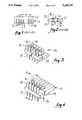
- FIG. 3is a perspective view of a pressure connector formed in accordance with the invention.
- FIG. 4is a perspective view of a connector assembly formed in accordance with the invention.
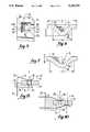
- FIG. 5is a bottom view of a conductor of a pressure connector formed in accordance with the invention showing a generally pyramidal shaped dimple formed on the conductor;
- FIG. 6is a cross section of the dimple taken along section line 6--6 of FIG. 5;
- FIG. 7is a cross section of the dimple taken along section line 7--7 of FIG. 5;
- FIG. 9is a perspective view of an alternate embodiment of a dimple formed with a generally pyramid shape having an octagonal base
- FIG. 10is a cross section similar to FIG. 8 showing an alternate embodiment connector formed with conductors that contact the circuit board on opposite sides of the circuit board;
- FIG. 11is a perspective view of an alternate embodiment of a dimple formed with a generally conical shape.
- the printed circuit board 10used in the construction of various electronic devices such as computers is shown.
- the printed circuit boardincludes a hard insulating substrate 12 on which various electronic components (not shown) are mounted.
- a plurality of printed circuit traces 14are formed on the substrate 12.
- the printed circuit traces 14connect the various electronic components and circuits formed on the substrate 12.
- the printed circuit traces 14are formed of a conductive material such as tin-lead and may be covered with an insulating material.
- the printed circuit traces 14terminate in a through hole 16.
- a cross section of a through hole 16is shown in FIG. 2.
- a through hole 16extends through the substrate 12 along a longitudinal axis 20.
- the through hole 16is located at an end of a printed circuit trace 14 and is adapted to electrically connect the circuit trace 14 with an electrical component located externally of the printed circuit board 10.
- the electrical component to be connectedmay be located on another printed circuit board.
- an electrical connectionhas been made using the through hole 16 by placing a wire lead (not shown) through the hole and then soldering the wire lead in the through hole 16.
- the through hole 16may be formed with a conductive material 18 such as gold plating or tin-lead solder.
- the conductive material 18is formed continuously with the printed circuit trace 14 and electrically connects to the printed circuit trace 14.
- the conductive material 18is formed along the inside diameter of the through hole 16 and circumjacent to the through hole 16 along its outer circumference on the top 22 and bottom 24 surfaces of the substrate 12. In the past a wire lead (not shown) of an electrical component to be connected to the through hole 16 is soldered to the conductive material 18.
- the pressure connector 26includes a substrate 28 formed of an insulating material.
- a plurality of conductors 30are attached to the substrate 28.
- the conductors 30include a free end 32 that is adapted to connect to another electrical lead or component (not shown) such as by soldering.
- the conductors 30also include a deflection arm 34 adapted to clamp to and maintain a positive contact force with a printed circuit board such as the printed circuit board 10 shown in FIG. 1.
- each deflection arm 34may be formed as a spring member shaped to exert a biasing or contact force against the printed circuit board 10.
- the pressure connector 26is clamped to the circuit board 10 with the circuit board 10 located between the substrate 28 of the pressure connector 26 and the deflection arms 34 of the conductors 30 of the pressure connector 26.
- a dimple 36(FIG. 5) is formed on a bottom surface 42 of each deflection arm 34. As will hereinafter be more fully explained, in use of the pressure connector 26, the dimples 36 are shaped to enter the through holes 16 and to make electrical contact with the conductive material 18 formed in the through holes 16. The dimples 36 are also formed to maintain an acceptable Hertzian force on the through hole 16 and to lock the connector 26 to the circuit board 10.
- the dimple 36is formed in a generally pyramidal shape. Alternately the dimple 36 may be formed in any other shape (such as with a conical shape) that permits the dimple 36 to enter the through hole 16 and contact the conductive material 18 within the through hole 16 along an edge, or along the outer circumference of the through hole 16.
- the dimple 36may also be formed to contact a flat contact pad 38 (FIG. 1) rather than a through hole 16 which may also be formed at the end of a printed circuit trace 14 (FIG. 1).
- the dimple 36is formed as a continuous surface from the bottom surface 42 of the deflection arm 34.
- the dimple 36includes a generally polygonal (i.e. square) shaped base portion 40 formed at the intersection of the dimple 36 and the bottom surface 42 of the deflection arm 34.
- the dimple 36includes a plurality of creased edges 62 formed to contact the through hole 16.
- the polygonal shaped base portion 40 of the dimple 36has a width "w" on each side.
- the width "w" (FIG. 6) of a side of the base portion 40 of the dimple 36is approximately 0.038 inches.
- the dimple 36extends from the bottom surface 34 of the deflection arm 34 to a height of "x" (FIG. 6).
- height "x"is approximately 0.012 inches.
- the pyramidal shaped dimple 36is four sided, with four creased edges 62.
- the four sides of the dimple 36taper to an apex 44.
- the apex 44does not come to a sharp point but rather is radiused with a radius of "r".
- radius "r"may be approximately 0.004 inches.
- the smooth apex 44is shaped such that it can slide over the printed circuit board prior to engagement in the through hole 16 without damage to the printed circuit board 22.
- a dimple 36'may also be formed substantially as shown in FIG. 9 with an octagonal 40' rather than a square shaped base portion.
- Dimple 36'(FIG. 9) is in all other respects similar to dimple 36 but has eight rather than four creased edges 62' which facilitate more points of contact with the conductive material 18 (FIG. 1) formed in and around the through hole 16.
- FIG. 8a cross section of the connector assembly, showing a dimple 36 located within a through hole 16 of a printed circuit board 10 is shown.
- the dimple 36extends into the through hole 16 and contacts the conductive material 18 formed in the through hole 16.
- the creased edges 62 of the dimple 36contact the conductive material 18 formed in the through hole 16 at at least one point within the hole 16.
- the spring force of the deflection arm 34provides the biasing or contact force "F" necessary to force the dimple 36 into the through hole 16 and maintain contact of the dimple 36 with the conductive material 18 within the through hole 16 or along a circumferential edge of the through hole 16.
- the force "F”is sufficient to create an acceptable amount of Hertzian Stress and to clamp the connector to the circuit board 10.
- the location of the dimple illustrated in FIG. 8is for an optimal alignment of the dimple 36 and through hole 16.
- the dimple 36is sized to enter and contact the conductive material 18 formed in a through hole 16 in a similar manner over a range of hole sizes.
- the shape of the dimple 36is such that contact is made at least one point of contact such as the point of contact of a creased edge 62 with the conductive material 18 formed in the through hole 16. There may however, be more than one point of contact if more than one creased edge 62 contacts the conductive material 18.
- contactmay include other portions of the dimple than the creased edges and may be along a circumferential edge of the through hole 16.
- the dimplehas been described as formed with a generally pyramid shape; it is understood that the dimple can be formed in other shapes.
- a generally conically shaped dimple 64is shown in FIG. 11.
- the conically shaped dimple 64is formed with a rounded apex 66 and smooth conical sidewalls 68. In use the sidewalls 8 of the dimple 64 make contact with the conductive material 18 within a through hole 16 substantially as previously described along a circumferential edge of the through hole 16.
- the connector of the inventionis adapted to provide a pressure connector for electrically connecting a row of through holes of a printed circuit board with other electrical devices or circuit boards.
- a dimple formed on a conductor of the pressure connectoris adapted to extend into and contact a range of through hole sizes. Contact can be made at least one point along the conductive material formed in the through hole or along a circumferential edge in or around the hole.
- the pressure connectoris formed to maintain a clamping force and a acceptable Hertzian Stress with the through hole.
Landscapes
- Coupling Device And Connection With Printed Circuit (AREA)
- Multi-Conductor Connections (AREA)
Abstract
Description
Claims (21)
Priority Applications (3)
| Application Number | Priority Date | Filing Date | Title |
|---|---|---|---|
| US07/911,774US5259767A (en) | 1992-07-10 | 1992-07-10 | Connector for a plated or soldered hole |
| EP93305056AEP0578420A1 (en) | 1992-07-10 | 1993-06-28 | Connector for a plated or soldered hole |
| JP5170422AJPH06203930A (en) | 1992-07-10 | 1993-07-09 | Connector for plated or brazed hole |
Applications Claiming Priority (1)
| Application Number | Priority Date | Filing Date | Title |
|---|---|---|---|
| US07/911,774US5259767A (en) | 1992-07-10 | 1992-07-10 | Connector for a plated or soldered hole |
Publications (1)
| Publication Number | Publication Date |
|---|---|
| US5259767Atrue US5259767A (en) | 1993-11-09 |
Family
ID=25430848
Family Applications (1)
| Application Number | Title | Priority Date | Filing Date |
|---|---|---|---|
| US07/911,774Expired - LifetimeUS5259767A (en) | 1992-07-10 | 1992-07-10 | Connector for a plated or soldered hole |
Country Status (3)
| Country | Link |
|---|---|
| US (1) | US5259767A (en) |
| EP (1) | EP0578420A1 (en) |
| JP (1) | JPH06203930A (en) |
Cited By (15)
| Publication number | Priority date | Publication date | Assignee | Title |
|---|---|---|---|---|
| US5472349A (en)* | 1994-10-31 | 1995-12-05 | The Whitaker Corporation | Surface mountable board edge connector |
| US5525763A (en)* | 1994-02-28 | 1996-06-11 | Robertshaw Controls Company | Printed circuit board arrangement |
| US5800186A (en)* | 1997-03-13 | 1998-09-01 | Framatome Connectors Usa, Inc. | Printed circuit board assembly |
| US5919064A (en)* | 1997-05-20 | 1999-07-06 | Framatome Connectors Usa Inc. | Card edge connector with similar shaped cantilevered beam spring contacts having multi-level contact areas |
| US6227867B1 (en)* | 1999-02-03 | 2001-05-08 | Hon Hai Precision Ind. Co., Ltd. | Method for performing double-sided SMT |
| US6312265B1 (en)* | 1999-08-27 | 2001-11-06 | Seagate Technology Llc | Double-sided single-print straddle mount assembly |
| US20030165051A1 (en)* | 2000-03-13 | 2003-09-04 | Kledzik Kenneth J. | Modular integrated circuit chip carrier |
| US20060189195A1 (en)* | 2005-02-23 | 2006-08-24 | Nec Corporation | Connector device |
| US20090191725A1 (en)* | 2008-01-24 | 2009-07-30 | Karl-Wilhelm Vogt | Connector for board-mounted led |
| US20130084759A1 (en)* | 2011-10-04 | 2013-04-04 | J.S.T. Mfg. Co., Ltd. | Contact and electrical connector |
| US8570688B1 (en)* | 2010-11-08 | 2013-10-29 | Magnecomp Corporation | Electrical connections to a microactuator in a hard disk drive suspension |
| US8830664B2 (en) | 2012-08-24 | 2014-09-09 | Apple Inc. | Complementary ground and support members |
| US9834008B2 (en) | 2014-06-24 | 2017-12-05 | Kyocera Corporation | Thermal head and thermal printer |
| DE102012021615B4 (en) | 2012-11-06 | 2021-08-05 | Phoenix Contact Gmbh & Co. Kg | PCB connection |
| US12396091B2 (en)* | 2021-11-15 | 2025-08-19 | AT&SAustria Technologie & Systemtechnik Aktiengesellschaft | Component carrier with a via containing a hardened filling material |
Citations (36)
| Publication number | Priority date | Publication date | Assignee | Title |
|---|---|---|---|---|
| US2990533A (en)* | 1958-04-09 | 1961-06-27 | Stokes D Hughes | Terminal post for circuit board |
| US3140907A (en)* | 1960-06-03 | 1964-07-14 | Int Standard Electric Corp | Electrical spring contact sockets |
| US3173732A (en)* | 1962-02-09 | 1965-03-16 | Brown Engineering Company Inc | Printed circuit board connector |
| US3215968A (en)* | 1960-12-21 | 1965-11-02 | Adolf L Herrmann | Printed circuit board connector |
| US3500285A (en)* | 1967-11-01 | 1970-03-10 | Baldwin Co D H | Multiple contact connector |
| US3518612A (en)* | 1966-08-06 | 1970-06-30 | Ibm | Connector assembly |
| US3731252A (en)* | 1971-03-22 | 1973-05-01 | Bendix Corp | Printed circuit board connector |
| US3795037A (en)* | 1970-05-05 | 1974-03-05 | Int Computers Ltd | Electrical connector devices |
| US3795884A (en)* | 1973-03-06 | 1974-03-05 | Amp Inc | Electrical connector formed from coil spring |
| US3829817A (en)* | 1971-10-07 | 1974-08-13 | Plessey Handel Investment Ag | Electrical connection devices |
| US3858154A (en)* | 1973-11-02 | 1974-12-31 | Gte Automatic Electric Lab Inc | Sliding three dimensional packaging technique |
| US3858961A (en)* | 1973-06-06 | 1975-01-07 | Itt | Printed circuit board connector |
| US3922051A (en)* | 1973-12-20 | 1975-11-25 | Amp Inc | Connector for alphanumeric display panels |
| US3954317A (en)* | 1974-02-27 | 1976-05-04 | Amp Incorporated | Elastomeric connector and its method of manufacture |
| US3960424A (en)* | 1974-10-02 | 1976-06-01 | Amp Incorporated | Multi-contact spring connector for board to board connections |
| US3969010A (en)* | 1974-05-17 | 1976-07-13 | E. I. Du Pont De Nemours And Company | Substrate with improved contact terminals |
| US3993383A (en)* | 1975-06-02 | 1976-11-23 | Vincent Marino | Printed circuit electrical connectors |
| US4003621A (en)* | 1975-06-16 | 1977-01-18 | Technical Wire Products, Inc. | Electrical connector employing conductive rectilinear elements |
| US4021091A (en)* | 1975-06-13 | 1977-05-03 | International Telephone And Telegraph Corporation | Zero force printed circuit board connector |
| US4057311A (en)* | 1976-11-11 | 1977-11-08 | Amp Incorporated | Elastomeric connector for parallel circuit boards |
| US4159154A (en)* | 1978-04-10 | 1979-06-26 | International Telephone And Telegraph Corporation | Zero insertion force connector |
| US4204205A (en)* | 1975-02-05 | 1980-05-20 | Kabushiki Kaisha Daini Seikosha | Electronic display device |
| US4295700A (en)* | 1978-10-12 | 1981-10-20 | Shin-Etsu Polymer Co., Ltd. | Interconnectors |
| US4445735A (en)* | 1980-12-05 | 1984-05-01 | Compagnie Internationale Pour L'informatique Cii-Honeywell Bull (Societe Anonyme) | Electrical connection device for high density contacts |
| US4508398A (en)* | 1983-09-26 | 1985-04-02 | Gte Automatic Electric Inc. | Printed circuit connecting device |
| US4521065A (en)* | 1983-09-27 | 1985-06-04 | General Motors Corporation | Socket connector for parallel circuit boards |
| US4538864A (en)* | 1983-01-18 | 1985-09-03 | Japan Aviation Electronics Industry | Contact element with locking means |
| US4575175A (en)* | 1983-10-27 | 1986-03-11 | Molex Incorporated | Edge connector for multiple printed circuit boards |
| US4577922A (en)* | 1985-04-04 | 1986-03-25 | Molex Incorporated | Laminated electrical connector arrangement |
| US4636018A (en)* | 1985-06-05 | 1987-01-13 | Amp Incorporated | Elastomeric electrical connector |
| US4699593A (en)* | 1986-01-14 | 1987-10-13 | Amp Incorporated | Connector having contact modules for a substrate such as an IC chip carrier |
| US4715820A (en)* | 1986-09-29 | 1987-12-29 | Amp Incorporated | Connection system for printed circuit boards |
| US4738625A (en)* | 1986-09-29 | 1988-04-19 | Bell Telephone Laboratories, Inc. | Electrical connectors for circuit panels |
| US4867689A (en)* | 1988-10-31 | 1989-09-19 | Amp Incorporated | Elastomeric connector assembly |
| US4976629A (en)* | 1989-10-04 | 1990-12-11 | Teledyne Kinetics | Zero insertion force dual in-line LCD connector |
| US4998886A (en)* | 1989-07-07 | 1991-03-12 | Teledyne Kinetics | High density stacking connector |
Family Cites Families (1)
| Publication number | Priority date | Publication date | Assignee | Title |
|---|---|---|---|---|
| GB2021334A (en)* | 1978-05-15 | 1979-11-28 | Promotors Ltd | Cartridge mechanism |
- 1992
- 1992-07-10USUS07/911,774patent/US5259767A/ennot_activeExpired - Lifetime
- 1993
- 1993-06-28EPEP93305056Apatent/EP0578420A1/ennot_activeWithdrawn
- 1993-07-09JPJP5170422Apatent/JPH06203930A/enactivePending
Patent Citations (37)
| Publication number | Priority date | Publication date | Assignee | Title |
|---|---|---|---|---|
| US2990533A (en)* | 1958-04-09 | 1961-06-27 | Stokes D Hughes | Terminal post for circuit board |
| US3140907A (en)* | 1960-06-03 | 1964-07-14 | Int Standard Electric Corp | Electrical spring contact sockets |
| US3215968A (en)* | 1960-12-21 | 1965-11-02 | Adolf L Herrmann | Printed circuit board connector |
| US3173732A (en)* | 1962-02-09 | 1965-03-16 | Brown Engineering Company Inc | Printed circuit board connector |
| US3518612A (en)* | 1966-08-06 | 1970-06-30 | Ibm | Connector assembly |
| US3500285A (en)* | 1967-11-01 | 1970-03-10 | Baldwin Co D H | Multiple contact connector |
| US3795037A (en)* | 1970-05-05 | 1974-03-05 | Int Computers Ltd | Electrical connector devices |
| US3731252A (en)* | 1971-03-22 | 1973-05-01 | Bendix Corp | Printed circuit board connector |
| US3829817A (en)* | 1971-10-07 | 1974-08-13 | Plessey Handel Investment Ag | Electrical connection devices |
| US3795884A (en)* | 1973-03-06 | 1974-03-05 | Amp Inc | Electrical connector formed from coil spring |
| US3858961A (en)* | 1973-06-06 | 1975-01-07 | Itt | Printed circuit board connector |
| US3858154A (en)* | 1973-11-02 | 1974-12-31 | Gte Automatic Electric Lab Inc | Sliding three dimensional packaging technique |
| US3922051A (en)* | 1973-12-20 | 1975-11-25 | Amp Inc | Connector for alphanumeric display panels |
| US3954317A (en)* | 1974-02-27 | 1976-05-04 | Amp Incorporated | Elastomeric connector and its method of manufacture |
| US3969010A (en)* | 1974-05-17 | 1976-07-13 | E. I. Du Pont De Nemours And Company | Substrate with improved contact terminals |
| US3960424A (en)* | 1974-10-02 | 1976-06-01 | Amp Incorporated | Multi-contact spring connector for board to board connections |
| US4204205A (en)* | 1975-02-05 | 1980-05-20 | Kabushiki Kaisha Daini Seikosha | Electronic display device |
| US3993383A (en)* | 1975-06-02 | 1976-11-23 | Vincent Marino | Printed circuit electrical connectors |
| US4021091A (en)* | 1975-06-13 | 1977-05-03 | International Telephone And Telegraph Corporation | Zero force printed circuit board connector |
| US4003621A (en)* | 1975-06-16 | 1977-01-18 | Technical Wire Products, Inc. | Electrical connector employing conductive rectilinear elements |
| US4057311A (en)* | 1976-11-11 | 1977-11-08 | Amp Incorporated | Elastomeric connector for parallel circuit boards |
| US4159154A (en)* | 1978-04-10 | 1979-06-26 | International Telephone And Telegraph Corporation | Zero insertion force connector |
| US4295700A (en)* | 1978-10-12 | 1981-10-20 | Shin-Etsu Polymer Co., Ltd. | Interconnectors |
| US4402562A (en)* | 1978-10-12 | 1983-09-06 | Shin-Etsu Polymer Co., Ltd. | Interconnectors |
| US4445735A (en)* | 1980-12-05 | 1984-05-01 | Compagnie Internationale Pour L'informatique Cii-Honeywell Bull (Societe Anonyme) | Electrical connection device for high density contacts |
| US4538864A (en)* | 1983-01-18 | 1985-09-03 | Japan Aviation Electronics Industry | Contact element with locking means |
| US4508398A (en)* | 1983-09-26 | 1985-04-02 | Gte Automatic Electric Inc. | Printed circuit connecting device |
| US4521065A (en)* | 1983-09-27 | 1985-06-04 | General Motors Corporation | Socket connector for parallel circuit boards |
| US4575175A (en)* | 1983-10-27 | 1986-03-11 | Molex Incorporated | Edge connector for multiple printed circuit boards |
| US4577922A (en)* | 1985-04-04 | 1986-03-25 | Molex Incorporated | Laminated electrical connector arrangement |
| US4636018A (en)* | 1985-06-05 | 1987-01-13 | Amp Incorporated | Elastomeric electrical connector |
| US4699593A (en)* | 1986-01-14 | 1987-10-13 | Amp Incorporated | Connector having contact modules for a substrate such as an IC chip carrier |
| US4715820A (en)* | 1986-09-29 | 1987-12-29 | Amp Incorporated | Connection system for printed circuit boards |
| US4738625A (en)* | 1986-09-29 | 1988-04-19 | Bell Telephone Laboratories, Inc. | Electrical connectors for circuit panels |
| US4867689A (en)* | 1988-10-31 | 1989-09-19 | Amp Incorporated | Elastomeric connector assembly |
| US4998886A (en)* | 1989-07-07 | 1991-03-12 | Teledyne Kinetics | High density stacking connector |
| US4976629A (en)* | 1989-10-04 | 1990-12-11 | Teledyne Kinetics | Zero insertion force dual in-line LCD connector |
Non-Patent Citations (12)
| Title |
|---|
| Advertisement Entitled Zone 3 Connectors, no date.* |
| Advertisement of Connection Technology, Interposer Multichip Socket, Copyright 1988.* |
| Advertisement of PCK Elastomerics, Inc., Carbon Stax Elastomeric Connectors.* |
| Brundy, Advertisement entitled Oikstack Feed Thru Stacking Connectors, no date.* |
| Brundy, Advertisement entitled Oikstack Feed-Thru Stacking Connectors, no date. |
| Connection Technology, Guidelines for Designing Elastomeric Connectors Into the Systems, Aug. 1987.* |
| Methode Electronics, Inc., Advertisement Entitled Surface Mate Surface Compression Connectors, 1989.* |
| PC Network, Advertisement Entitled SMT Connectors for High Density Packaging, p. 33, Aug. 1990.* |
| PCK Elastomerics, Inc., Advertisement Entitled Parallel Board Connector, no date.* |
| Tecknit, Advertisement re Zebra, the New Connector Technology, dated Apr., 1982.* |
| Ufheil, Joseph C., Compression Mount Technology for Surface Mate Connectors, pp. 663 645, no date.* |
| Ufheil, Joseph C., Compression Mount Technology for Surface Mate Connectors, pp. 663-645, no date. |
Cited By (21)
| Publication number | Priority date | Publication date | Assignee | Title |
|---|---|---|---|---|
| US5525763A (en)* | 1994-02-28 | 1996-06-11 | Robertshaw Controls Company | Printed circuit board arrangement |
| US5687476A (en)* | 1994-02-28 | 1997-11-18 | Robertshaw Controls Company | Method of making printed circuit arrangement |
| US5472349A (en)* | 1994-10-31 | 1995-12-05 | The Whitaker Corporation | Surface mountable board edge connector |
| EP0709931A3 (en)* | 1994-10-31 | 1997-01-02 | Whitaker Corp | Surface-mounted circuit edge connector |
| US5800186A (en)* | 1997-03-13 | 1998-09-01 | Framatome Connectors Usa, Inc. | Printed circuit board assembly |
| US5919064A (en)* | 1997-05-20 | 1999-07-06 | Framatome Connectors Usa Inc. | Card edge connector with similar shaped cantilevered beam spring contacts having multi-level contact areas |
| US6227867B1 (en)* | 1999-02-03 | 2001-05-08 | Hon Hai Precision Ind. Co., Ltd. | Method for performing double-sided SMT |
| US6312265B1 (en)* | 1999-08-27 | 2001-11-06 | Seagate Technology Llc | Double-sided single-print straddle mount assembly |
| US7102892B2 (en)* | 2000-03-13 | 2006-09-05 | Legacy Electronics, Inc. | Modular integrated circuit chip carrier |
| US20030165051A1 (en)* | 2000-03-13 | 2003-09-04 | Kledzik Kenneth J. | Modular integrated circuit chip carrier |
| US7796400B2 (en) | 2000-03-13 | 2010-09-14 | Legacy Electronics, Inc. | Modular integrated circuit chip carrier |
| US20060189195A1 (en)* | 2005-02-23 | 2006-08-24 | Nec Corporation | Connector device |
| US7255586B2 (en)* | 2005-02-23 | 2007-08-14 | Nec Corporation | Connector device |
| US20090191725A1 (en)* | 2008-01-24 | 2009-07-30 | Karl-Wilhelm Vogt | Connector for board-mounted led |
| US7828557B2 (en)* | 2008-01-24 | 2010-11-09 | Bjb Gmbh & Co. Kg | Connector for board-mounted LED |
| US8570688B1 (en)* | 2010-11-08 | 2013-10-29 | Magnecomp Corporation | Electrical connections to a microactuator in a hard disk drive suspension |
| US20130084759A1 (en)* | 2011-10-04 | 2013-04-04 | J.S.T. Mfg. Co., Ltd. | Contact and electrical connector |
| US8830664B2 (en) | 2012-08-24 | 2014-09-09 | Apple Inc. | Complementary ground and support members |
| DE102012021615B4 (en) | 2012-11-06 | 2021-08-05 | Phoenix Contact Gmbh & Co. Kg | PCB connection |
| US9834008B2 (en) | 2014-06-24 | 2017-12-05 | Kyocera Corporation | Thermal head and thermal printer |
| US12396091B2 (en)* | 2021-11-15 | 2025-08-19 | AT&SAustria Technologie & Systemtechnik Aktiengesellschaft | Component carrier with a via containing a hardened filling material |
Also Published As
| Publication number | Publication date |
|---|---|
| JPH06203930A (en) | 1994-07-22 |
| EP0578420A1 (en) | 1994-01-12 |
Similar Documents
| Publication | Publication Date | Title |
|---|---|---|
| US5259767A (en) | Connector for a plated or soldered hole | |
| US4655517A (en) | Electrical connector | |
| US6033245A (en) | Self-aligning electrical connector | |
| US3953096A (en) | Free standing mother-daughter printed circuit board contact arrangement | |
| US5669774A (en) | Ball grid array socket | |
| US6534856B1 (en) | Sockets for “springed” semiconductor devices | |
| US4191440A (en) | Electrical connector for coupling power leads to circuit boards | |
| US6042389A (en) | Low profile connector | |
| US7874870B1 (en) | Coaxial cable connector with a connection terminal having a resilient tongue section | |
| US5366380A (en) | Spring biased tapered contact elements for electrical connectors and integrated circuit packages | |
| US5709574A (en) | Surface-mountable socket connector | |
| US5562462A (en) | Reduced crosstalk and shielded adapter for mounting an integrated chip package on a circuit board like member | |
| US7559770B2 (en) | Socket with high performance electrical connectors | |
| US7338294B2 (en) | Pressure contact connector | |
| JP2001167831A (en) | Crimped grid array connector | |
| EP0017358B1 (en) | Electrical connector housing with a mounting peg | |
| US5411409A (en) | Component mounting arrangement | |
| US20080124957A1 (en) | Electrical contact background of the invention | |
| JPH02215064A (en) | Connector for integrated circuit board | |
| US7402066B2 (en) | Low insertion force socket with lead-in mechanism background of the invention | |
| US6887114B2 (en) | Electrical connector with high performance contacts | |
| US4943846A (en) | Pin grid array having seperate posts and socket contacts | |
| US6280248B1 (en) | Hold-down element for electrical and/or electronic components | |
| US5453700A (en) | Test clip contact arrangement | |
| US4181385A (en) | Low profile socket for circuit board with gas vents for fixed position soldering |
Legal Events
| Date | Code | Title | Description |
|---|---|---|---|
| AS | Assignment | Owner name:TELEDYNE KINETICS, A CORPORATION OF CA, CALIFORNIA Free format text:ASSIGNMENT OF ASSIGNORS INTEREST.;ASSIGNORS:KURBIKOFF, PETER A.;CHITAMITARA, APICHART N.;REEL/FRAME:006236/0240 Effective date:19920717 | |
| STCF | Information on status: patent grant | Free format text:PATENTED CASE | |
| AS | Assignment | Owner name:TELEDYNE INDUSTRIES, INC., CALIFORNIA Free format text:ASSIGNMENT OF ASSIGNORS INTEREST;ASSIGNOR:TELEDYNE KINETICS;REEL/FRAME:008259/0561 Effective date:19961118 | |
| FPAY | Fee payment | Year of fee payment:4 | |
| AS | Assignment | Owner name:TELEDYNE TECHNOLOGIES INCORPORATED, CALIFORNIA Free format text:ASSIGNMENT OF ASSIGNORS INTEREST;ASSIGNOR:TELEDYNE INDUSTRIES, INC.;REEL/FRAME:010703/0172 Effective date:19991129 | |
| FEPP | Fee payment procedure | Free format text:PAYOR NUMBER ASSIGNED (ORIGINAL EVENT CODE: ASPN); ENTITY STATUS OF PATENT OWNER: LARGE ENTITY | |
| FPAY | Fee payment | Year of fee payment:8 | |
| FPAY | Fee payment | Year of fee payment:12 |