US5256073A - Electrical connectors for direct connection to plated through holes in circuit board - Google Patents
Electrical connectors for direct connection to plated through holes in circuit boardDownload PDFInfo
- Publication number
- US5256073A US5256073AUS07/892,684US89268492AUS5256073AUS 5256073 AUS5256073 AUS 5256073AUS 89268492 AUS89268492 AUS 89268492AUS 5256073 AUS5256073 AUS 5256073A
- Authority
- US
- United States
- Prior art keywords
- electrical connector
- spring contact
- contact element
- contact
- board
- Prior art date
- Legal status (The legal status is an assumption and is not a legal conclusion. Google has not performed a legal analysis and makes no representation as to the accuracy of the status listed.)
- Expired - Fee Related
Links
Images


Classifications
- H—ELECTRICITY
- H01—ELECTRIC ELEMENTS
- H01R—ELECTRICALLY-CONDUCTIVE CONNECTIONS; STRUCTURAL ASSOCIATIONS OF A PLURALITY OF MUTUALLY-INSULATED ELECTRICAL CONNECTING ELEMENTS; COUPLING DEVICES; CURRENT COLLECTORS
- H01R12/00—Structural associations of a plurality of mutually-insulated electrical connecting elements, specially adapted for printed circuits, e.g. printed circuit boards [PCB], flat or ribbon cables, or like generally planar structures, e.g. terminal strips, terminal blocks; Coupling devices specially adapted for printed circuits, flat or ribbon cables, or like generally planar structures; Terminals specially adapted for contact with, or insertion into, printed circuits, flat or ribbon cables, or like generally planar structures
- H01R12/50—Fixed connections
- H01R12/51—Fixed connections for rigid printed circuits or like structures
- H01R12/55—Fixed connections for rigid printed circuits or like structures characterised by the terminals
- H01R12/58—Fixed connections for rigid printed circuits or like structures characterised by the terminals terminals for insertion into holes
- H—ELECTRICITY
- H01—ELECTRIC ELEMENTS
- H01R—ELECTRICALLY-CONDUCTIVE CONNECTIONS; STRUCTURAL ASSOCIATIONS OF A PLURALITY OF MUTUALLY-INSULATED ELECTRICAL CONNECTING ELEMENTS; COUPLING DEVICES; CURRENT COLLECTORS
- H01R12/00—Structural associations of a plurality of mutually-insulated electrical connecting elements, specially adapted for printed circuits, e.g. printed circuit boards [PCB], flat or ribbon cables, or like generally planar structures, e.g. terminal strips, terminal blocks; Coupling devices specially adapted for printed circuits, flat or ribbon cables, or like generally planar structures; Terminals specially adapted for contact with, or insertion into, printed circuits, flat or ribbon cables, or like generally planar structures
- H01R12/70—Coupling devices
- H01R12/71—Coupling devices for rigid printing circuits or like structures
- H01R12/72—Coupling devices for rigid printing circuits or like structures coupling with the edge of the rigid printed circuits or like structures
- H01R12/722—Coupling devices for rigid printing circuits or like structures coupling with the edge of the rigid printed circuits or like structures coupling devices mounted on the edge of the printed circuits
- H01R12/724—Coupling devices for rigid printing circuits or like structures coupling with the edge of the rigid printed circuits or like structures coupling devices mounted on the edge of the printed circuits containing contact members forming a right angle
- H—ELECTRICITY
- H05—ELECTRIC TECHNIQUES NOT OTHERWISE PROVIDED FOR
- H05K—PRINTED CIRCUITS; CASINGS OR CONSTRUCTIONAL DETAILS OF ELECTRIC APPARATUS; MANUFACTURE OF ASSEMBLAGES OF ELECTRICAL COMPONENTS
- H05K1/00—Printed circuits
- H05K1/18—Printed circuits structurally associated with non-printed electric components
- H05K1/182—Printed circuits structurally associated with non-printed electric components associated with components mounted in the printed circuit board, e.g. insert mounted components [IMC]
- H05K1/184—Components including terminals inserted in holes through the printed circuit board and connected to printed contacts on the walls of the holes or at the edges thereof or protruding over or into the holes
- H—ELECTRICITY
- H05—ELECTRIC TECHNIQUES NOT OTHERWISE PROVIDED FOR
- H05K—PRINTED CIRCUITS; CASINGS OR CONSTRUCTIONAL DETAILS OF ELECTRIC APPARATUS; MANUFACTURE OF ASSEMBLAGES OF ELECTRICAL COMPONENTS
- H05K2201/00—Indexing scheme relating to printed circuits covered by H05K1/00
- H05K2201/10—Details of components or other objects attached to or integrated in a printed circuit board
- H05K2201/10227—Other objects, e.g. metallic pieces
- H05K2201/10393—Clamping a component by an element or a set of elements
- H—ELECTRICITY
- H05—ELECTRIC TECHNIQUES NOT OTHERWISE PROVIDED FOR
- H05K—PRINTED CIRCUITS; CASINGS OR CONSTRUCTIONAL DETAILS OF ELECTRIC APPARATUS; MANUFACTURE OF ASSEMBLAGES OF ELECTRICAL COMPONENTS
- H05K2203/00—Indexing scheme relating to apparatus or processes for manufacturing printed circuits covered by H05K3/00
- H05K2203/17—Post-manufacturing processes
- H05K2203/176—Removing, replacing or disconnecting component; Easily removable component
Definitions
- This inventionrelates generally to electrical connectors for connecting daughter cards to a backplane, midplane, harness card or the like (hereinafter referred to as a "mother board” or “mother card”). More particularly, the invention relates to a self-centering contact, high density connector for connecting a daughter card directly to the plated through holes of the mother card, where the high density connector may be configured as a standard connector, a zero insertion force connector (ZIF) or as a sequential/selectively engaging pin connector.
- ZIFzero insertion force connector
- the electrical connector artsare crowded arts with many categories and subcategories of connectors.
- One such categoryare connectors which are used to connect two printed circuit boards (PCB).
- PCBprinted circuit boards
- the first PCBis a mother board
- the second PCBis a daughter board at right angles to the mother board
- the connectionis a pluggable connection such that replacement of cards and/or expansion of the system is easily accomplished.
- the standard connectors for permitting such a non-permanent right angle interfacerequire placing a first piece of hardware (e.g. in the case of conventional inverted DIN connectors, the pin or male part) on the mother board, and a second piece of hardware (e.g. The mating female receptacle of a right angle connector) on the daughter board.
- a connector for connecting a daughter board to a mother boardis provided with a plurality of contact elements which are bent over a radius of approximately ninety degrees, and a dielectric housing for housing the contact elements.
- the connectoris used in conjunction with a means for establishing and maintaining force on the contact elements so as to keep them engaged in plated through holes in the mother board.
- the contact elementsare pins with first ends which typically are soldered to through holes in the daughter board, mid-sections which are crimped and bent through ninety degrees, and second ends which have a converging portion and which terminate in contact portions which are tapered in cross section and which are used to make contact with the contact-quality plated through holes of the mother board.
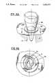
- FIG. 1is a perspective view of a column section of the connector invention prior to insertion of the preformed spring contact elements into the housing.
- FIG. 3ais a cross sectional view of the connector through line A--A of FIG. 2b.
- FIG. 3bis an enlarged cross sectional view of the self-centering tapered funnel of the housing shown in FIG. 3a with a contact element located therein in an unengaged extended position, and in engaged depressed positions.
- FIG. 3cis a partially cut-away top view of the connector taken along line C--C of FIG. 3a.
- FIG. 4ais a perspective enlarged view of the tapered end of a single preferred split-cone contact element in contact with a preferred embodiment of the mother card plated through hole.
- FIG. 4bis a cross sectional view of the tapered end of a single preferred split-cone contact element of the connector through line B--B of FIG. 4a.
- FIG. 4cis a force diagram for a typical contact element of the connector, showing both axial insertion (hold-in) and mating contact normal forces.
- FIG. 4dis a cross sectional view of an embodiment of the invention where two connectors are connected to a mid-plane.
- FIG. 6ais a side view of a contact element of the invention prior to its formation into a spring contact.
- FIG. 6bis partial cross sectional view of the connector of the invention where the contact element of FIG. 6a is shown in the process of being formed into a preloaded spring contact through the use of a tool and the housing.
- FIGS. 7a and 7bare partially cut-away side views of the alternative connector of the selective contact actuation or ZIF embodiment of the invention.
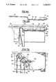
- FIG. 8ais a perspective view of a spring loaded jack screw for use in conjunction with a plurality of connectors so as to maintain the connectors in contact with the mother board.
- FIG. 8bis a side view of an alternative embodiment of a part of the spring loaded jack screw of FIG. 6a.
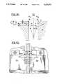
- FIG. 9ais a perspective view of a first magnet system for use in conjunction with a plurality of connectors so as to maintain the connectors in contact with the mother board.
- FIG. 9bis a perspective view of a second magnet system for use in conjunction with a plurality of connectors so as to maintain the connectors in contact with the mother board.
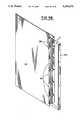
- FIGS. 10a and 10bare respectively a partially cut-away perspective view and enlarged cross-sectional view of a first alternate embodiment of the mother board of the invention which incorporates an alignment grid which permits increased alignment tolerance for the connector invention.
- FIG. 11is an enlarged cross-section of a second alternate embodiment of the mother board which includes a special compliant layer over a standard PCB board for enhancing contact performance.
- FIGS. 1, 2a, 2b, 3a-3c, and 4a-4cshow a first preferred connector assembly of the invention.
- the connector assembly 10typically comprises a plurality of contact elements 20, and a dielectric housing 30 for housing the contact elements.
- the contact elements 30are spring pins with first ends 32, second ends 34, and a middle bend section 36.
- the first ends 32 of pins 20extend through holes 39 in the daughter board 40 and are preferably soldered to the back side 41 of the daughter board. At least a portion of the first ends 32 is preferably v-shaped to help align the first ends in the holes 39 of the daughter board 40.
- the shape of first ends 32also provides stiffness, and helps in preloading the contacts as will be discussed hereinafter.
- the second ends 34 of the contact elements 30are basically comprised of a neck portion 35 which may be channel shaped for stiffness, and a tapered contact portion 38. As seen in FIG. 3b, connecting the neck portion 35 to the contact portion 38 is an angled portion 37 which acts in conjunction with the housing to provide self-alignment and preloading as will be described hereinafter.
- the mid-sections 36 of pins 20are preferably crimped to cause pins 20 to form a spring. As shown in FIG. 1, pins 20 are preferably crimped to first form a one hundred eighty degree bend and then a minus ninety degree bend, and are thus essentially bent through ninety degrees. If desired, a simple bend of ninety degrees could be used, provided mid-sections 36 form spring elements. As seen in FIG. 3a in phantom, when contact portions 38 of second ends 34 of pins 30 engage the mother board 50, the mid-sections 36 resiliently deflect away from the mother board 50; i.e. the mid-sections 36 are compliant along the mating axis. In so doing, the mid-sections 36 provide pins 30 with a mating force.
- the contact portions 38 of the second ends 34 of contact elements 20are tapered in cross section, with the cross section becoming larger further away from the end or tip of the contact element.
- the contact portions 38are used to make contact with the plated through holes 51 of the mother board 50.
- the contact portions 38 of the second ends 34are the preferred split (bifurcated) cones (as seen in FIGS. 4a and 4b)
- contactis made between the connector 10 and the mother board 50 at two points 53a, 53b (radius contact "points") for each contact element 20 and through hole 51.
- the contactis made between the tapered portion (i.e. the contact portion 38) of the contact element 20 and the rim of hole 51; i.e.
- contact portion 38In making contact, because contact portion 38 is bifurcated, it resiliently compresses as it is pushed into hole 51, and therefore extends into hole 51 further than it might have otherwise. As a result, the surface of contact portion 38 wipes along the rim of hole 51 as it makes contact providing desired "wipe" and enhanced contact.
- the mother board 50provides a normal contact force F N /2 (shown as the hypotenuse of the triangle).
- Each normal contact forceis the result of two perpendicular forces; an axial force of twenty-five grams opposite to the mating force (as required to provide an equal but opposite force to the axial mating force); and a force perpendicular to the axial force.
- the perpendicular forces to the axial forcesare equal and opposite each other and therefore cancel.
- the tapered contact portion 38 of pin 20may take any of numerous embodiments.
- the most conventional candidateswould be a sphere, a cone, a four edged pyramid, and a three edged pyramid or tetrahedron.
- each such contact portionis tapered and would therefore contact the hole.
- the contact, as seen in FIGS. 5a3-5d3,might range from a three point contact for the tetrahedron, to irregular annular contact for the sphere and cone. While a four point contact would be expected from the four-edged pyramid, it is possible that only two or three contact points would be made.
- the compliant bifurcated cone of FIG. 4a and 4bis the preferred embodiment, followed by the tetrahedron.
- the housing 30includes side walls 60 which separate and electrically insulate each column of contact pins 20; the side walls 60 extending perpendicularly from top wall 62. Also extending perpendicularly from top wall 62 is front wall 64 having a plurality of openings 66 for permitting at least a portion of tapered contact portions 38 (and preferably the entire tapered contact portion) of contact pins 20 to extend therethrough. Openings 66 are preferably tapered funnels which are arranged to interact with the angled portion 37 of the second ends 34 of the contact pins as will be hereinafter described.
- each guide wallextends slightly past the middle bent portion 36 of the pin contact below it, but only as far as the second end 34 of the pin above it.
- FIG. 3bexplores the axial and lateral tolerances built into the connector contact pins relative to the plated through holes of the mother board.
- angled portions 37contact the funnel-like openings 66 and thereby center themselves herein in a nominal position.
- the openings 66act as a stop to the contact spring pins 20 to cause the spring pins to be preloaded in the housing, as will be discussed hereinafter.
- the contact portions 38 of the pins 20extend out of the housing 30 by a desired amount.
- the pins 20When the contact pins 20 engage the mother board holes, the pins 20 are pushed backward (as seen in phantom) such that the angled portion 37 of the second ends 34 of the pins no longer contacts the funnel-like openings 66 of the housing 30.
- lateral movement of the second end of the pinis expedited in all directions, as the passage for the second end of the pin defined by adjacent side walls 60 and adjacent guide walls 68 of the housing 30 is wider than the second ends 34 of the pins.
- the further pins 20are pushed backward, the more second ends 34 can move laterally in any direction in the housing passage.
- side walls 60 of housing 30preferably include side-wall locking tabs 72 (preferably two per contact) which hold adjacent rows of contacts in a preloaded manner at different fixing points relative to the daughter board 40 but at identical fixing points relative to the ninety-degree bend portion 36 of the contact elements 20.
- the locking tabs 72provide a restriction between adjacent side walls 60 through which the v-shaped first end 32 of pins 20 are forced during assembly. After the v-shaped first end 32 deforms and passes through the tabs 72, they cannot return past the tabs 72.
- the manufacture of the spring contacts for the preferred connector of the inventioncan be completed, and the spring contacts can be preloaded during the assembly of the connector.
- the contact element 20 of the inventionis seen in FIG. 6a prior to its insertion into the housing 30.
- Contact element 20includes contact portion 38, angled portion 37, second end 34, middle portion 36, and first end 32. As shown, part of first end 32 is v or u shaped, and part of second end 34 is ribbed or channel shaped. Middle portion 36 is provided with a "dog's-leg" bend.
- manufacture/assemblythe contact element 20 of FIG.
- first end 32 of the contact elementis forced downward by a press (not shown), with the v-shaped first end 32 being forced past locking tabs 72, until the first end 32 is brought into contact with the angled surface 142 of bending fixture 140.
- first end 32springs back and bending fixture 140 is removed.
- first end 32can only spring back to the vertical position of FIG.
- contact elements 30are preloaded. Also, because the first end 32 of contact element 20 does not spring back to its original shape of FIG. 6a when locking tabs 72 are not present, but rather assumes the position of the spring contact elements of FIG. 1a, the process of bending the contact element 20 is seen to form the contacts into spring contacts. Thus, a connector whose preloaded spring contacts are actually partially manufactured during assembly is provided.
- FIGS. 7a and 7bTwo embodiments for retracting contact portions 28 are shown in FIGS. 7a and 7b.
- retracting cams 180are provided and can be fixed to side walls 60. By rotating the cams as indicated, the middle portion 26 of the spring contacts 20 is forced backward (as shown in phantom), thereby drawing contact portions 28 back towards or into housing 30.
- the threaded section of rod 90extends past the front face 64 of connectors 10, through a hole in mother board (back plane) 50 and is arranged to engage a tapped bushing 95 located on a stiffening channel 97 which runs along the mother board 50.
- Stiffening channel 97serves to stiffen the mother board 50 so as to prevent bowing of the same due to the large forces exerted by the leaf spring in keeping connectors 10 mated in the through holes of the mother board 50.
- the entire arrangement of FIG. 8ais particularly advantageous where there are a large number of contacts in a connector and the total force of engagement is appreciable as the connector is held to its portion of the mother board without putting undo stress on either the daughter card, the rest of the mother card, or the mother card cage structure.
- FIGS. 9a and 9bOther means of establishing and maintaining force on the connectors are shown in FIGS. 9a and 9b.
- simple bar magnets 98aare attached to the daughter PCB 40, with one magnet on either side of the connectors 10. Identical poles of each magnet are arranged to face the mother board (not shown) which is provided with one or more steel plates 99a as an attracting surface.
- horseshoe magnets 98bare located alongside each connector 10. A steel strip 99b s provided on the mother board to provide an attracting surface for the magnets.
- FIGS. 10a, 10b, and 11changes to the mother board are shown for enhancing the invention.
- grid elementsare provided on the surface 55 of the mother board 50 around each hole 51.
- the grid elements 105are shaped so as guide the contact portion 38 of the contact elements 20 towards hole 51 without stubbing contact portion 38.
- the preferred grid structure shapeis substantially parabolic. However, many other shapes can be utilized.
- Grid elements 105provide the connector invention with additional misalignment tolerance relative to the mother board which is particularly useful where relatively large spacing is used between mother board holes. Without the grid elements, the maximum misalignment tolerance of the spring elements 20 of connector 10 with a hole 5 is the radius of the hole. With grid elements 105, the maximum alignment tolerance of the pins to the holes is significantly increased to one half the distance between the holes 51. Such an alignment tolerance is very large compared to other connectors of the art.
- an additional compliant layer 110is shown as an integral part of a specially laminated mother board 50.
- Compliant layer 110is preferably laminated to a conventional FR-4 printed circuit board and provides an appropriate matching compliance for the contact elements 20.
- through hole 51 of the mother board 50is provided with standard copper plating 112.
- gold over nickel (although other contact-quality platings could be used) plating layer 114is provided atop the copper plating 112 and serves to provide the mating contact surface for the spring contacts 20.
- the compliant layer 110can be provided in situations where additional wipe is required, and/or where frequent insertion of daughter cards is expected.
Landscapes
- Coupling Device And Connection With Printed Circuit (AREA)
Abstract
Description
Claims (33)
Priority Applications (3)
| Application Number | Priority Date | Filing Date | Title |
|---|---|---|---|
| US07/892,684US5256073A (en) | 1989-06-13 | 1992-05-27 | Electrical connectors for direct connection to plated through holes in circuit board |
| US08/038,175US5366380A (en) | 1989-06-13 | 1993-03-29 | Spring biased tapered contact elements for electrical connectors and integrated circuit packages |
| US08/143,443US5425649A (en) | 1989-06-13 | 1993-10-26 | Connector system having switching and testing functions using tapered spring contact elements and actuators therefor |
Applications Claiming Priority (3)
| Application Number | Priority Date | Filing Date | Title |
|---|---|---|---|
| US07/366,546US4966556A (en) | 1989-06-13 | 1989-06-13 | Electrical connector for direct connection to plated through holes in circuit board |
| US60552190A | 1990-10-29 | 1990-10-29 | |
| US07/892,684US5256073A (en) | 1989-06-13 | 1992-05-27 | Electrical connectors for direct connection to plated through holes in circuit board |
Related Parent Applications (1)
| Application Number | Title | Priority Date | Filing Date |
|---|---|---|---|
| US60552190AContinuation | 1989-06-13 | 1990-10-29 |
Related Child Applications (2)
| Application Number | Title | Priority Date | Filing Date |
|---|---|---|---|
| US08/038,175Continuation-In-PartUS5366380A (en) | 1989-06-13 | 1993-03-29 | Spring biased tapered contact elements for electrical connectors and integrated circuit packages |
| US08/143,443Continuation-In-PartUS5425649A (en) | 1989-06-13 | 1993-10-26 | Connector system having switching and testing functions using tapered spring contact elements and actuators therefor |
Publications (1)
| Publication Number | Publication Date |
|---|---|
| US5256073Atrue US5256073A (en) | 1993-10-26 |
Family
ID=27408757
Family Applications (1)
| Application Number | Title | Priority Date | Filing Date |
|---|---|---|---|
| US07/892,684Expired - Fee RelatedUS5256073A (en) | 1989-06-13 | 1992-05-27 | Electrical connectors for direct connection to plated through holes in circuit board |
Country Status (1)
| Country | Link |
|---|---|
| US (1) | US5256073A (en) |
Cited By (13)
| Publication number | Priority date | Publication date | Assignee | Title |
|---|---|---|---|---|
| US5425649A (en)* | 1989-06-13 | 1995-06-20 | General Datacomm, Inc. | Connector system having switching and testing functions using tapered spring contact elements and actuators therefor |
| US5468160A (en)* | 1994-08-16 | 1995-11-21 | The Whitaker Corporation | Mounting bracket for an electrical connector |
| US5597317A (en)* | 1995-08-11 | 1997-01-28 | W. L. Gore & Associates, Inc. | Surface mating electrical connector |
| FR2791514A1 (en)* | 1999-03-22 | 2000-09-29 | Proner Comatel Sa | Electronic component/printed circuit pin in hollow reflow connection element having metal conductor section forming upper section/base pin printed circuit connection and integral tongue connection. |
| US6554654B1 (en)* | 2001-12-31 | 2003-04-29 | Hewlett-Packard Development Company, L.P. | Multi-pin edge connector for circuit board |
| US6597901B1 (en)* | 1997-11-28 | 2003-07-22 | Nokia Mobile Phones Limited | Device having a headset socket |
| US20030143873A1 (en)* | 2002-01-28 | 2003-07-31 | Harting Electro-Optics Gmbh & Co. Kg | Connector with movable contact elements |
| US6846185B1 (en)* | 2003-08-14 | 2005-01-25 | Lite-On Technology Corporation | Blind mating apparatus |
| CN100397289C (en)* | 2004-12-29 | 2008-06-25 | 威盛电子股份有限公司 | Mounting components for the motherboard |
| US20090137161A1 (en)* | 2007-11-26 | 2009-05-28 | Tyco Electronics Corporation | Electrical contact with retention latch |
| US20100144167A1 (en)* | 2008-12-05 | 2010-06-10 | Fedder James L | Electrical Connector System |
| CN101574773B (en)* | 2008-05-08 | 2010-12-15 | 华通电脑股份有限公司 | Positioning pin assembling device of printed circuit board |
| US20130065410A1 (en)* | 2010-03-12 | 2013-03-14 | Detlef NEHM | Plug-type connector |
Citations (65)
| Publication number | Priority date | Publication date | Assignee | Title |
|---|---|---|---|---|
| US3144527A (en)* | 1961-09-13 | 1964-08-11 | Manuel J Tolegian | Magnetic electrical coupling |
| US3215968A (en)* | 1960-12-21 | 1965-11-02 | Adolf L Herrmann | Printed circuit board connector |
| US3290636A (en)* | 1963-09-30 | 1966-12-06 | Northern Electric Co | Thin-film circuit connector |
| US3404362A (en)* | 1966-07-29 | 1968-10-01 | Bendix Corp | Selective indexing guide device for electrical connectors of printed circuit cards |
| US3407378A (en)* | 1966-05-24 | 1968-10-22 | Hersey Sparling Meter Company | Electrical contact system |
| US3430182A (en)* | 1967-04-27 | 1969-02-25 | Nasa | Electrical feed-through connection for printed circuit boards and printed cable |
| US3447249A (en)* | 1965-05-07 | 1969-06-03 | Intertrading Corp Establishmen | Electronic building set |
| US3504328A (en)* | 1968-01-03 | 1970-03-31 | Berg Electronics Inc | Circuit board eyelet |
| US3550062A (en)* | 1967-12-26 | 1970-12-22 | Gen Electric | Connector and mounting device for printed wiring boards |
| US3601762A (en)* | 1969-08-15 | 1971-08-24 | Vernitron Corp | Electrical connector |
| US3783433A (en)* | 1971-01-18 | 1974-01-01 | Litton Systems Inc | Solderless electrical connection system |
| US3810258A (en)* | 1972-07-11 | 1974-05-07 | W Mathauser | Quick connect electrical coupler |
| US3885215A (en)* | 1974-01-07 | 1975-05-20 | Unit Process Assemblies | Electrode assembly for measuring the effective thickness of thru-hole plating in circuit board workpieces or the like |
| US3899231A (en)* | 1973-12-21 | 1975-08-12 | Aeronutronic Ford Corp | Electrical connector |
| US3996516A (en)* | 1973-08-23 | 1976-12-07 | Lm-Electronic Luther & Maelzer | Apparatus and process for testing printed circuits |
| US4004298A (en)* | 1975-03-31 | 1977-01-25 | Sinai Hospital Of Detroit | Magnetically aligned releasable connector |
| US4012093A (en)* | 1971-08-25 | 1977-03-15 | The Deutsch Company Electronic Components Division | Connector arrangement for thin, deflectable conductors |
| US4042880A (en)* | 1974-01-07 | 1977-08-16 | Unit Process Assemblies, Inc. | Electrode assembly for measuring the effective thickness of thru-hole plating circuit board workpieces |
| US4050769A (en)* | 1976-03-18 | 1977-09-27 | Elfab Corporation | Electrical connector |
| US4095867A (en)* | 1974-10-10 | 1978-06-20 | Bunker Ramo Corporation | Component connection system |
| US4118090A (en)* | 1977-05-23 | 1978-10-03 | Luigi Giovanni Del Mei | Electrical contact devices |
| DE2845632A1 (en)* | 1977-10-28 | 1979-05-03 | Ferranti Ltd | ELECTRICAL CONNECTOR |
| US4164704A (en)* | 1976-11-01 | 1979-08-14 | Metropolitan Circuits, Inc. | Plural probe circuit card fixture using a vacuum collapsed membrane to hold the card against the probes |
| US4175810A (en)* | 1976-11-22 | 1979-11-27 | Augat Inc. | Electrical interconnection boards with lead sockets mounted therein and method for making same |
| US4242657A (en)* | 1978-08-02 | 1980-12-30 | Gustave Chaillot | Electric connector |
| US4245189A (en)* | 1979-06-14 | 1981-01-13 | Upa Technology, Inc. | Probe assembly for measuring conductivity of plated through holes |
| US4270826A (en)* | 1979-02-01 | 1981-06-02 | Thomas & Betts Corporation | Zero insertion force connector |
| US4321532A (en)* | 1978-03-16 | 1982-03-23 | Luna L Jack | Repairable spring probe assembly |
| US4381134A (en)* | 1981-03-13 | 1983-04-26 | Bell Telephone Laboratories, Incorporated | Electrical connector for plated-through holes |
| US4428640A (en)* | 1981-12-24 | 1984-01-31 | Industrial Electronic Hardware | Protective means for multiple pin connectors |
| US4443756A (en)* | 1980-11-25 | 1984-04-17 | Lightbody James D | Apparatus and method for testing circuit boards |
| US4448466A (en)* | 1981-11-12 | 1984-05-15 | Ncr Corporation | Low insertion force connector for printed circuit boards |
| US4479685A (en)* | 1983-06-20 | 1984-10-30 | Exxon Production Research Co. | Flexible magnetic electrical connector and cable incorporating that connector |
| US4498722A (en)* | 1983-12-05 | 1985-02-12 | Amp Incorporated | Latch device for ZIF card edge connectors |
| US4504101A (en)* | 1983-08-29 | 1985-03-12 | Gte Automatic Electric Inc. | Low insertion force connection arrangement |
| US4510553A (en)* | 1983-01-24 | 1985-04-09 | Burroughs Corporation | Electromechanical assembly for aligning, discharging, and sequentially engaging conductors of a P.C. board with a backplane |
| US4526429A (en)* | 1983-07-26 | 1985-07-02 | Augat Inc. | Compliant pin for solderless termination to a printed wiring board |
| US4528500A (en)* | 1980-11-25 | 1985-07-09 | Lightbody James D | Apparatus and method for testing circuit boards |
| US4533203A (en)* | 1983-12-07 | 1985-08-06 | Amp Incorporated | Connector for printed circuit boards |
| US4541678A (en)* | 1983-07-01 | 1985-09-17 | Trw Inc. | Printed circuit board indexing and locking device |
| US4548452A (en)* | 1983-06-29 | 1985-10-22 | International Business Machines Corporation | High-density electrical contact pad pattern |
| US4550962A (en)* | 1983-05-18 | 1985-11-05 | Erni Elektroapparate Gmbh | Solderless electrical connector assembly |
| US4571542A (en)* | 1982-06-30 | 1986-02-18 | Japan Synthetic Rubber Co., Ltd. | Method and unit for inspecting printed wiring boards |
| US4587596A (en)* | 1984-04-09 | 1986-05-06 | Amp Incorporated | High density mother/daughter circuit board connector |
| DE3441480A1 (en)* | 1984-11-13 | 1986-05-15 | MANIA Elektronik Automatisation Entwicklung und Gerätebau GmbH, 6384 Schmitten | CONTACT PEN |
| DE3500227A1 (en)* | 1985-01-05 | 1986-07-10 | Riba-Prüftechnik GmbH, 7801 Schallstadt | Probe needle |
| US4606589A (en)* | 1984-01-12 | 1986-08-19 | H & V Services | Compliant pin |
| US4652066A (en)* | 1984-09-26 | 1987-03-24 | Siemens Aktiengesellschaft | Insertible electric assembly |
| US4675600A (en)* | 1984-05-17 | 1987-06-23 | Geo International Corporation | Testing apparatus for plated through-holes on printed circuit boards, and probe therefor |
| US4691979A (en)* | 1983-08-04 | 1987-09-08 | Manda R & D | Compliant press-fit electrical contact |
| US4701703A (en)* | 1979-08-13 | 1987-10-20 | Philip M. Hinderstein | Bed-of-pins test fixture |
| US4707655A (en)* | 1984-06-12 | 1987-11-17 | Feinmetall Gmbh | Contact for multicontact probe assembly |
| US4717844A (en)* | 1985-03-04 | 1988-01-05 | Hitachi, Ltd. | Programmable logic array circuit with a decreased number of product terms |
| US4721908A (en)* | 1985-09-16 | 1988-01-26 | Mania Elektronik Automatisation Entwicklung Und Geratebau Gmbh | Apparatus for electronically testing printed cirucit boards or the like |
| US4724383A (en)* | 1985-05-03 | 1988-02-09 | Testsystems, Inc. | PC board test fixture |
| US4730086A (en)* | 1984-07-19 | 1988-03-08 | Alps Electric Co., Ltd. | Film-covered terminal |
| US4735587A (en)* | 1986-02-12 | 1988-04-05 | Specialty Electronics, Inc. | Pin header with board retention tail |
| US4744764A (en)* | 1986-05-27 | 1988-05-17 | Rogers Corporation | Connector arrangement |
| US4755149A (en)* | 1986-08-15 | 1988-07-05 | Amp Incorporated | Blind mating connector |
| US4758186A (en)* | 1985-07-25 | 1988-07-19 | Legrand | Side connecting terminal block |
| US4789352A (en)* | 1987-12-02 | 1988-12-06 | Amp Incorporated | Power connector having linearly moving cam for daughter card |
| US4793817A (en)* | 1985-02-27 | 1988-12-27 | Karl Neumayer, Erzeugung Und Vertreib Von Kabeln, Drahten Isolierten Leitungen Und Elektromaterial Gesellschaft Mit Beschrankter Haftung | Contact pin |
| US4793816A (en)* | 1987-07-20 | 1988-12-27 | Industrial Electronic Hardware | Terminal protector for circuit board connector |
| US4795362A (en)* | 1988-03-03 | 1989-01-03 | Gte Communication Systems, Inc. | Circuit connector for use with printed wiring board |
| US4795977A (en)* | 1987-03-19 | 1989-01-03 | Pacific Western Systems, Inc. | Interface system for interfacing a device tester to a device under test |
- 1992
- 1992-05-27USUS07/892,684patent/US5256073A/ennot_activeExpired - Fee Related
Patent Citations (65)
| Publication number | Priority date | Publication date | Assignee | Title |
|---|---|---|---|---|
| US3215968A (en)* | 1960-12-21 | 1965-11-02 | Adolf L Herrmann | Printed circuit board connector |
| US3144527A (en)* | 1961-09-13 | 1964-08-11 | Manuel J Tolegian | Magnetic electrical coupling |
| US3290636A (en)* | 1963-09-30 | 1966-12-06 | Northern Electric Co | Thin-film circuit connector |
| US3447249A (en)* | 1965-05-07 | 1969-06-03 | Intertrading Corp Establishmen | Electronic building set |
| US3407378A (en)* | 1966-05-24 | 1968-10-22 | Hersey Sparling Meter Company | Electrical contact system |
| US3404362A (en)* | 1966-07-29 | 1968-10-01 | Bendix Corp | Selective indexing guide device for electrical connectors of printed circuit cards |
| US3430182A (en)* | 1967-04-27 | 1969-02-25 | Nasa | Electrical feed-through connection for printed circuit boards and printed cable |
| US3550062A (en)* | 1967-12-26 | 1970-12-22 | Gen Electric | Connector and mounting device for printed wiring boards |
| US3504328A (en)* | 1968-01-03 | 1970-03-31 | Berg Electronics Inc | Circuit board eyelet |
| US3601762A (en)* | 1969-08-15 | 1971-08-24 | Vernitron Corp | Electrical connector |
| US3783433A (en)* | 1971-01-18 | 1974-01-01 | Litton Systems Inc | Solderless electrical connection system |
| US4012093A (en)* | 1971-08-25 | 1977-03-15 | The Deutsch Company Electronic Components Division | Connector arrangement for thin, deflectable conductors |
| US3810258A (en)* | 1972-07-11 | 1974-05-07 | W Mathauser | Quick connect electrical coupler |
| US3996516A (en)* | 1973-08-23 | 1976-12-07 | Lm-Electronic Luther & Maelzer | Apparatus and process for testing printed circuits |
| US3899231A (en)* | 1973-12-21 | 1975-08-12 | Aeronutronic Ford Corp | Electrical connector |
| US3885215A (en)* | 1974-01-07 | 1975-05-20 | Unit Process Assemblies | Electrode assembly for measuring the effective thickness of thru-hole plating in circuit board workpieces or the like |
| US4042880A (en)* | 1974-01-07 | 1977-08-16 | Unit Process Assemblies, Inc. | Electrode assembly for measuring the effective thickness of thru-hole plating circuit board workpieces |
| US4095867A (en)* | 1974-10-10 | 1978-06-20 | Bunker Ramo Corporation | Component connection system |
| US4004298A (en)* | 1975-03-31 | 1977-01-25 | Sinai Hospital Of Detroit | Magnetically aligned releasable connector |
| US4050769A (en)* | 1976-03-18 | 1977-09-27 | Elfab Corporation | Electrical connector |
| US4164704A (en)* | 1976-11-01 | 1979-08-14 | Metropolitan Circuits, Inc. | Plural probe circuit card fixture using a vacuum collapsed membrane to hold the card against the probes |
| US4175810A (en)* | 1976-11-22 | 1979-11-27 | Augat Inc. | Electrical interconnection boards with lead sockets mounted therein and method for making same |
| US4118090A (en)* | 1977-05-23 | 1978-10-03 | Luigi Giovanni Del Mei | Electrical contact devices |
| DE2845632A1 (en)* | 1977-10-28 | 1979-05-03 | Ferranti Ltd | ELECTRICAL CONNECTOR |
| US4321532A (en)* | 1978-03-16 | 1982-03-23 | Luna L Jack | Repairable spring probe assembly |
| US4242657A (en)* | 1978-08-02 | 1980-12-30 | Gustave Chaillot | Electric connector |
| US4270826A (en)* | 1979-02-01 | 1981-06-02 | Thomas & Betts Corporation | Zero insertion force connector |
| US4245189A (en)* | 1979-06-14 | 1981-01-13 | Upa Technology, Inc. | Probe assembly for measuring conductivity of plated through holes |
| US4701703A (en)* | 1979-08-13 | 1987-10-20 | Philip M. Hinderstein | Bed-of-pins test fixture |
| US4528500A (en)* | 1980-11-25 | 1985-07-09 | Lightbody James D | Apparatus and method for testing circuit boards |
| US4443756A (en)* | 1980-11-25 | 1984-04-17 | Lightbody James D | Apparatus and method for testing circuit boards |
| US4381134A (en)* | 1981-03-13 | 1983-04-26 | Bell Telephone Laboratories, Incorporated | Electrical connector for plated-through holes |
| US4448466A (en)* | 1981-11-12 | 1984-05-15 | Ncr Corporation | Low insertion force connector for printed circuit boards |
| US4428640A (en)* | 1981-12-24 | 1984-01-31 | Industrial Electronic Hardware | Protective means for multiple pin connectors |
| US4571542A (en)* | 1982-06-30 | 1986-02-18 | Japan Synthetic Rubber Co., Ltd. | Method and unit for inspecting printed wiring boards |
| US4510553A (en)* | 1983-01-24 | 1985-04-09 | Burroughs Corporation | Electromechanical assembly for aligning, discharging, and sequentially engaging conductors of a P.C. board with a backplane |
| US4550962A (en)* | 1983-05-18 | 1985-11-05 | Erni Elektroapparate Gmbh | Solderless electrical connector assembly |
| US4479685A (en)* | 1983-06-20 | 1984-10-30 | Exxon Production Research Co. | Flexible magnetic electrical connector and cable incorporating that connector |
| US4548452A (en)* | 1983-06-29 | 1985-10-22 | International Business Machines Corporation | High-density electrical contact pad pattern |
| US4541678A (en)* | 1983-07-01 | 1985-09-17 | Trw Inc. | Printed circuit board indexing and locking device |
| US4526429A (en)* | 1983-07-26 | 1985-07-02 | Augat Inc. | Compliant pin for solderless termination to a printed wiring board |
| US4691979A (en)* | 1983-08-04 | 1987-09-08 | Manda R & D | Compliant press-fit electrical contact |
| US4504101A (en)* | 1983-08-29 | 1985-03-12 | Gte Automatic Electric Inc. | Low insertion force connection arrangement |
| US4498722A (en)* | 1983-12-05 | 1985-02-12 | Amp Incorporated | Latch device for ZIF card edge connectors |
| US4533203A (en)* | 1983-12-07 | 1985-08-06 | Amp Incorporated | Connector for printed circuit boards |
| US4606589A (en)* | 1984-01-12 | 1986-08-19 | H & V Services | Compliant pin |
| US4587596A (en)* | 1984-04-09 | 1986-05-06 | Amp Incorporated | High density mother/daughter circuit board connector |
| US4675600A (en)* | 1984-05-17 | 1987-06-23 | Geo International Corporation | Testing apparatus for plated through-holes on printed circuit boards, and probe therefor |
| US4707655A (en)* | 1984-06-12 | 1987-11-17 | Feinmetall Gmbh | Contact for multicontact probe assembly |
| US4730086A (en)* | 1984-07-19 | 1988-03-08 | Alps Electric Co., Ltd. | Film-covered terminal |
| US4652066A (en)* | 1984-09-26 | 1987-03-24 | Siemens Aktiengesellschaft | Insertible electric assembly |
| DE3441480A1 (en)* | 1984-11-13 | 1986-05-15 | MANIA Elektronik Automatisation Entwicklung und Gerätebau GmbH, 6384 Schmitten | CONTACT PEN |
| DE3500227A1 (en)* | 1985-01-05 | 1986-07-10 | Riba-Prüftechnik GmbH, 7801 Schallstadt | Probe needle |
| US4793817A (en)* | 1985-02-27 | 1988-12-27 | Karl Neumayer, Erzeugung Und Vertreib Von Kabeln, Drahten Isolierten Leitungen Und Elektromaterial Gesellschaft Mit Beschrankter Haftung | Contact pin |
| US4717844A (en)* | 1985-03-04 | 1988-01-05 | Hitachi, Ltd. | Programmable logic array circuit with a decreased number of product terms |
| US4724383A (en)* | 1985-05-03 | 1988-02-09 | Testsystems, Inc. | PC board test fixture |
| US4758186A (en)* | 1985-07-25 | 1988-07-19 | Legrand | Side connecting terminal block |
| US4721908A (en)* | 1985-09-16 | 1988-01-26 | Mania Elektronik Automatisation Entwicklung Und Geratebau Gmbh | Apparatus for electronically testing printed cirucit boards or the like |
| US4735587A (en)* | 1986-02-12 | 1988-04-05 | Specialty Electronics, Inc. | Pin header with board retention tail |
| US4744764A (en)* | 1986-05-27 | 1988-05-17 | Rogers Corporation | Connector arrangement |
| US4755149A (en)* | 1986-08-15 | 1988-07-05 | Amp Incorporated | Blind mating connector |
| US4795977A (en)* | 1987-03-19 | 1989-01-03 | Pacific Western Systems, Inc. | Interface system for interfacing a device tester to a device under test |
| US4793816A (en)* | 1987-07-20 | 1988-12-27 | Industrial Electronic Hardware | Terminal protector for circuit board connector |
| US4789352A (en)* | 1987-12-02 | 1988-12-06 | Amp Incorporated | Power connector having linearly moving cam for daughter card |
| US4795362A (en)* | 1988-03-03 | 1989-01-03 | Gte Communication Systems, Inc. | Circuit connector for use with printed wiring board |
Non-Patent Citations (3)
| Title |
|---|
| IBM Bulletin, Faure vol. 17, No. 5, Controlled Direction Buckling Beam, Oct. 1974.* |
| IBM Bulletin, Faure, vol. 17, No. 2, p. 444, Jul. 1974.* |
| IBM Bulletin, Schick, vol. 6, No. 10, p. 5, Mar. 1964.* |
Cited By (21)
| Publication number | Priority date | Publication date | Assignee | Title |
|---|---|---|---|---|
| US5425649A (en)* | 1989-06-13 | 1995-06-20 | General Datacomm, Inc. | Connector system having switching and testing functions using tapered spring contact elements and actuators therefor |
| US5468160A (en)* | 1994-08-16 | 1995-11-21 | The Whitaker Corporation | Mounting bracket for an electrical connector |
| US5597317A (en)* | 1995-08-11 | 1997-01-28 | W. L. Gore & Associates, Inc. | Surface mating electrical connector |
| EP0758807A3 (en)* | 1995-08-11 | 1998-11-18 | W.L. GORE & ASSOCIATES, INC. | Surface mating electrical connector |
| US6597901B1 (en)* | 1997-11-28 | 2003-07-22 | Nokia Mobile Phones Limited | Device having a headset socket |
| FR2791514A1 (en)* | 1999-03-22 | 2000-09-29 | Proner Comatel Sa | Electronic component/printed circuit pin in hollow reflow connection element having metal conductor section forming upper section/base pin printed circuit connection and integral tongue connection. |
| US6554654B1 (en)* | 2001-12-31 | 2003-04-29 | Hewlett-Packard Development Company, L.P. | Multi-pin edge connector for circuit board |
| US20030143873A1 (en)* | 2002-01-28 | 2003-07-31 | Harting Electro-Optics Gmbh & Co. Kg | Connector with movable contact elements |
| EP1335454A1 (en)* | 2002-01-28 | 2003-08-13 | Harting Electro-Optics GmbH & Co. KG. | Connector with collapsible contact elements |
| US6857908B2 (en) | 2002-01-28 | 2005-02-22 | Gmbh & Co. Kg | Connector with movable contact elements |
| US20050037636A1 (en)* | 2003-08-14 | 2005-02-17 | Lan Chi Feng | Blind mating apparatus |
| US6846185B1 (en)* | 2003-08-14 | 2005-01-25 | Lite-On Technology Corporation | Blind mating apparatus |
| CN100397289C (en)* | 2004-12-29 | 2008-06-25 | 威盛电子股份有限公司 | Mounting components for the motherboard |
| US20090137161A1 (en)* | 2007-11-26 | 2009-05-28 | Tyco Electronics Corporation | Electrical contact with retention latch |
| US7604518B2 (en)* | 2007-11-26 | 2009-10-20 | Tyco Electronics Corporation | Electrical contact with retention latch |
| CN101574773B (en)* | 2008-05-08 | 2010-12-15 | 华通电脑股份有限公司 | Positioning pin assembling device of printed circuit board |
| US20100144167A1 (en)* | 2008-12-05 | 2010-06-10 | Fedder James L | Electrical Connector System |
| US7976318B2 (en)* | 2008-12-05 | 2011-07-12 | Tyco Electronics Corporation | Electrical connector system |
| TWI476997B (en)* | 2008-12-05 | 2015-03-11 | Tyco Electronics Corp | Electrical connector system |
| US20130065410A1 (en)* | 2010-03-12 | 2013-03-14 | Detlef NEHM | Plug-type connector |
| US8790142B2 (en)* | 2010-03-12 | 2014-07-29 | Phoenix Contact Gmbh & Co. Kg | Plug-type connector |
Similar Documents
| Publication | Publication Date | Title |
|---|---|---|
| US4966556A (en) | Electrical connector for direct connection to plated through holes in circuit board | |
| US4898539A (en) | Surface mount HDI contact | |
| EP0132664B1 (en) | Compliant pin for solderless termination to a printed wiring board | |
| US5256073A (en) | Electrical connectors for direct connection to plated through holes in circuit board | |
| US5366380A (en) | Spring biased tapered contact elements for electrical connectors and integrated circuit packages | |
| JP2996256B2 (en) | Apparatus and method for mounting multiple pin components to a circuit board | |
| USRE33005E (en) | Electrical connector | |
| US5562462A (en) | Reduced crosstalk and shielded adapter for mounting an integrated chip package on a circuit board like member | |
| US5482474A (en) | Edge-mountable circuit board connector | |
| US11005204B2 (en) | High speed electrical connector assembly | |
| US5215471A (en) | Electrical connectors having tapered spring contact elements for direct mating to holes | |
| EP2051338B1 (en) | Electrical connector assembly | |
| EP0729653A4 (en) | Right angle electrical connector and insertion tool | |
| EP0555368B1 (en) | Electrical connectors having tapered spring contact element | |
| JP2001516131A (en) | Electrical connector assembly | |
| US5511984A (en) | Electrical connector | |
| US6074220A (en) | Direct circuit to circuit stored energy connector | |
| JP2000513492A (en) | Compression connector | |
| CA1215150A (en) | Connector | |
| US5127838A (en) | Plated electrical connectors | |
| EP0499431A1 (en) | Lanced hold-downs | |
| US5938456A (en) | Low profile electrical connector | |
| US3876274A (en) | Receptacles employing high density array of overlapping self-adjustable contacts | |
| US5009606A (en) | Separable electrical connector | |
| US4718166A (en) | Method of making a connector |
Legal Events
| Date | Code | Title | Description |
|---|---|---|---|
| AS | Assignment | Owner name:BANK OF NEW YORK, AS AGENT, THE, NEW YORK Free format text:SECURITY INTEREST;ASSIGNOR:GENERAL DATACOMM, INC.;REEL/FRAME:007030/0214 Effective date:19940601 | |
| AS | Assignment | Owner name:BANK OF NEW YORK COMMERCIAL CORPORATION, THE, AS A Free format text:ASSIGNMENT OF ASSIGNORS INTEREST;ASSIGNOR:BANK OF NEW YORK, THE, AS AGENT;REEL/FRAME:007869/0253 Effective date:19951130 | |
| FPAY | Fee payment | Year of fee payment:4 | |
| AS | Assignment | Owner name:BNY FINANCIAL CORPORATION, AS AGENT SUCCESSOR BY M Free format text:RELEASE OF SECURITY INTEREST;ASSIGNOR:GENERAL DATACOMM, INC.;REEL/FRAME:008773/0992 Effective date:19971023 Owner name:TRANSAMERICA BUSINESS CREDIT CORPORATION, AS AGENT Free format text:SECURITY AGREEMENT;ASSIGNOR:GENERAL DATACOMM, INC.;REEL/FRAME:008829/0038 Effective date:19971022 | |
| AS | Assignment | Owner name:FOOTHILL CAPITAL CORPORATION, AS AGENT, CALIFORNIA Free format text:SECURITY INTEREST;ASSIGNORS:GENERAL DATACOMM, INC., A CORP. OF DE;GENERAL DATACOMM INDUSTRIES, INC., A CORP. OF DE;REEL/FRAME:009935/0139 Effective date:19990514 | |
| AS | Assignment | Owner name:GENERAL DATACOMM, INC., CONNECTICUT Free format text:RELEASE BY SECURED PARTY;ASSIGNOR:TRANSAMERICA BUSINESS CREDIT CORPORATION, AS AGENT;REEL/FRAME:009942/0001 Effective date:19990513 Owner name:GENERAL DATACOMM INDUSTRIES, INC., (DELAWARE CORPO Free format text:RELEASE BY SECURED PARTY;ASSIGNOR:TRANSAMERICA BUSINESS CREDIT CORPORATION, AS AGENT;REEL/FRAME:009942/0001 Effective date:19990513 | |
| REMI | Maintenance fee reminder mailed | ||
| LAPS | Lapse for failure to pay maintenance fees | ||
| STCH | Information on status: patent discontinuation | Free format text:PATENT EXPIRED DUE TO NONPAYMENT OF MAINTENANCE FEES UNDER 37 CFR 1.362 | |
| FP | Lapsed due to failure to pay maintenance fee | Effective date:20011026 | |
| AS | Assignment | Owner name:ABLECO FINANCE LLC, NEW YORK Free format text:SECURITY AGREEMENT;ASSIGNORS:GENERAL DATACOMM INDUSTRIES, INC.;GENERAL DATACOMM, INC.;REEL/FRAME:014108/0580 Effective date:20030915 | |
| AS | Assignment | Owner name:GENERAL DATACOMM, INC., CONNECTICUT Free format text:RELEASE OF SECURITY INTEREST;ASSIGNOR:ABLECO FINANCE LLC;REEL/FRAME:019864/0279 Effective date:20070730 Owner name:GENERAL DATACOMM INDUSTRIES, INC., CONNECTICUT Free format text:RELEASE OF SECURITY INTEREST;ASSIGNOR:ABLECO FINANCE LLC;REEL/FRAME:019864/0279 Effective date:20070730 |