US5255431A - Method of using frozen epoxy for placing pin-mounted components in a circuit module - Google Patents
Method of using frozen epoxy for placing pin-mounted components in a circuit moduleDownload PDFInfo
- Publication number
- US5255431A US5255431AUS07/904,719US90471992AUS5255431AUS 5255431 AUS5255431 AUS 5255431AUS 90471992 AUS90471992 AUS 90471992AUS 5255431 AUS5255431 AUS 5255431A
- Authority
- US
- United States
- Prior art keywords
- epoxy
- frozen
- bodies
- circuit module
- accordance
- Prior art date
- Legal status (The legal status is an assumption and is not a legal conclusion. Google has not performed a legal analysis and makes no representation as to the accuracy of the status listed.)
- Expired - Fee Related
Links
Images


Classifications
- H—ELECTRICITY
- H01—ELECTRIC ELEMENTS
- H01L—SEMICONDUCTOR DEVICES NOT COVERED BY CLASS H10
- H01L24/00—Arrangements for connecting or disconnecting semiconductor or solid-state bodies; Methods or apparatus related thereto
- H01L24/80—Methods for connecting semiconductor or other solid state bodies using means for bonding being attached to, or being formed on, the surface to be connected
- H01L24/83—Methods for connecting semiconductor or other solid state bodies using means for bonding being attached to, or being formed on, the surface to be connected using a layer connector
- H—ELECTRICITY
- H01—ELECTRIC ELEMENTS
- H01L—SEMICONDUCTOR DEVICES NOT COVERED BY CLASS H10
- H01L24/00—Arrangements for connecting or disconnecting semiconductor or solid-state bodies; Methods or apparatus related thereto
- H01L24/01—Means for bonding being attached to, or being formed on, the surface to be connected, e.g. chip-to-package, die-attach, "first-level" interconnects; Manufacturing methods related thereto
- H01L24/18—High density interconnect [HDI] connectors; Manufacturing methods related thereto
- H01L24/19—Manufacturing methods of high density interconnect preforms
- H—ELECTRICITY
- H01—ELECTRIC ELEMENTS
- H01L—SEMICONDUCTOR DEVICES NOT COVERED BY CLASS H10
- H01L24/00—Arrangements for connecting or disconnecting semiconductor or solid-state bodies; Methods or apparatus related thereto
- H01L24/01—Means for bonding being attached to, or being formed on, the surface to be connected, e.g. chip-to-package, die-attach, "first-level" interconnects; Manufacturing methods related thereto
- H01L24/26—Layer connectors, e.g. plate connectors, solder or adhesive layers; Manufacturing methods related thereto
- H01L24/28—Structure, shape, material or disposition of the layer connectors prior to the connecting process
- H01L24/29—Structure, shape, material or disposition of the layer connectors prior to the connecting process of an individual layer connector
- H—ELECTRICITY
- H05—ELECTRIC TECHNIQUES NOT OTHERWISE PROVIDED FOR
- H05K—PRINTED CIRCUITS; CASINGS OR CONSTRUCTIONAL DETAILS OF ELECTRIC APPARATUS; MANUFACTURE OF ASSEMBLAGES OF ELECTRICAL COMPONENTS
- H05K3/00—Apparatus or processes for manufacturing printed circuits
- H05K3/0011—Working of insulating substrates or insulating layers
- H05K3/0017—Etching of the substrate by chemical or physical means
- H05K3/0026—Etching of the substrate by chemical or physical means by laser ablation
- H05K3/0032—Etching of the substrate by chemical or physical means by laser ablation of organic insulating material
- H05K3/0035—Etching of the substrate by chemical or physical means by laser ablation of organic insulating material of blind holes, i.e. having a metal layer at the bottom
- H—ELECTRICITY
- H05—ELECTRIC TECHNIQUES NOT OTHERWISE PROVIDED FOR
- H05K—PRINTED CIRCUITS; CASINGS OR CONSTRUCTIONAL DETAILS OF ELECTRIC APPARATUS; MANUFACTURE OF ASSEMBLAGES OF ELECTRICAL COMPONENTS
- H05K3/00—Apparatus or processes for manufacturing printed circuits
- H05K3/30—Assembling printed circuits with electric components, e.g. with resistor
- H05K3/32—Assembling printed circuits with electric components, e.g. with resistor electrically connecting electric components or wires to printed circuits
- H05K3/321—Assembling printed circuits with electric components, e.g. with resistor electrically connecting electric components or wires to printed circuits by conductive adhesives
- H—ELECTRICITY
- H01—ELECTRIC ELEMENTS
- H01L—SEMICONDUCTOR DEVICES NOT COVERED BY CLASS H10
- H01L2224/00—Indexing scheme for arrangements for connecting or disconnecting semiconductor or solid-state bodies and methods related thereto as covered by H01L24/00
- H01L2224/01—Means for bonding being attached to, or being formed on, the surface to be connected, e.g. chip-to-package, die-attach, "first-level" interconnects; Manufacturing methods related thereto
- H01L2224/02—Bonding areas; Manufacturing methods related thereto
- H01L2224/04—Structure, shape, material or disposition of the bonding areas prior to the connecting process
- H01L2224/04105—Bonding areas formed on an encapsulation of the semiconductor or solid-state body, e.g. bonding areas on chip-scale packages
- H—ELECTRICITY
- H01—ELECTRIC ELEMENTS
- H01L—SEMICONDUCTOR DEVICES NOT COVERED BY CLASS H10
- H01L2224/00—Indexing scheme for arrangements for connecting or disconnecting semiconductor or solid-state bodies and methods related thereto as covered by H01L24/00
- H01L2224/01—Means for bonding being attached to, or being formed on, the surface to be connected, e.g. chip-to-package, die-attach, "first-level" interconnects; Manufacturing methods related thereto
- H01L2224/10—Bump connectors; Manufacturing methods related thereto
- H01L2224/15—Structure, shape, material or disposition of the bump connectors after the connecting process
- H01L2224/16—Structure, shape, material or disposition of the bump connectors after the connecting process of an individual bump connector
- H01L2224/161—Disposition
- H01L2224/16151—Disposition the bump connector connecting between a semiconductor or solid-state body and an item not being a semiconductor or solid-state body, e.g. chip-to-substrate, chip-to-passive
- H01L2224/16221—Disposition the bump connector connecting between a semiconductor or solid-state body and an item not being a semiconductor or solid-state body, e.g. chip-to-substrate, chip-to-passive the body and the item being stacked
- H01L2224/16225—Disposition the bump connector connecting between a semiconductor or solid-state body and an item not being a semiconductor or solid-state body, e.g. chip-to-substrate, chip-to-passive the body and the item being stacked the item being non-metallic, e.g. insulating substrate with or without metallisation
- H01L2224/16237—Disposition the bump connector connecting between a semiconductor or solid-state body and an item not being a semiconductor or solid-state body, e.g. chip-to-substrate, chip-to-passive the body and the item being stacked the item being non-metallic, e.g. insulating substrate with or without metallisation the bump connector connecting to a bonding area disposed in a recess of the surface of the item
- H—ELECTRICITY
- H01—ELECTRIC ELEMENTS
- H01L—SEMICONDUCTOR DEVICES NOT COVERED BY CLASS H10
- H01L2224/00—Indexing scheme for arrangements for connecting or disconnecting semiconductor or solid-state bodies and methods related thereto as covered by H01L24/00
- H01L2224/01—Means for bonding being attached to, or being formed on, the surface to be connected, e.g. chip-to-package, die-attach, "first-level" interconnects; Manufacturing methods related thereto
- H01L2224/26—Layer connectors, e.g. plate connectors, solder or adhesive layers; Manufacturing methods related thereto
- H01L2224/28—Structure, shape, material or disposition of the layer connectors prior to the connecting process
- H01L2224/29—Structure, shape, material or disposition of the layer connectors prior to the connecting process of an individual layer connector
- H01L2224/29001—Core members of the layer connector
- H01L2224/29099—Material
- H01L2224/291—Material with a principal constituent of the material being a metal or a metalloid, e.g. boron [B], silicon [Si], germanium [Ge], arsenic [As], antimony [Sb], tellurium [Te] and polonium [Po], and alloys thereof
- H01L2224/29101—Material with a principal constituent of the material being a metal or a metalloid, e.g. boron [B], silicon [Si], germanium [Ge], arsenic [As], antimony [Sb], tellurium [Te] and polonium [Po], and alloys thereof the principal constituent melting at a temperature of less than 400°C
- H—ELECTRICITY
- H01—ELECTRIC ELEMENTS
- H01L—SEMICONDUCTOR DEVICES NOT COVERED BY CLASS H10
- H01L2224/00—Indexing scheme for arrangements for connecting or disconnecting semiconductor or solid-state bodies and methods related thereto as covered by H01L24/00
- H01L2224/01—Means for bonding being attached to, or being formed on, the surface to be connected, e.g. chip-to-package, die-attach, "first-level" interconnects; Manufacturing methods related thereto
- H01L2224/26—Layer connectors, e.g. plate connectors, solder or adhesive layers; Manufacturing methods related thereto
- H01L2224/28—Structure, shape, material or disposition of the layer connectors prior to the connecting process
- H01L2224/29—Structure, shape, material or disposition of the layer connectors prior to the connecting process of an individual layer connector
- H01L2224/29001—Core members of the layer connector
- H01L2224/29099—Material
- H01L2224/2919—Material with a principal constituent of the material being a polymer, e.g. polyester, phenolic based polymer, epoxy
- H—ELECTRICITY
- H01—ELECTRIC ELEMENTS
- H01L—SEMICONDUCTOR DEVICES NOT COVERED BY CLASS H10
- H01L2224/00—Indexing scheme for arrangements for connecting or disconnecting semiconductor or solid-state bodies and methods related thereto as covered by H01L24/00
- H01L2224/01—Means for bonding being attached to, or being formed on, the surface to be connected, e.g. chip-to-package, die-attach, "first-level" interconnects; Manufacturing methods related thereto
- H01L2224/26—Layer connectors, e.g. plate connectors, solder or adhesive layers; Manufacturing methods related thereto
- H01L2224/28—Structure, shape, material or disposition of the layer connectors prior to the connecting process
- H01L2224/29—Structure, shape, material or disposition of the layer connectors prior to the connecting process of an individual layer connector
- H01L2224/29001—Core members of the layer connector
- H01L2224/29099—Material
- H01L2224/29198—Material with a principal constituent of the material being a combination of two or more materials in the form of a matrix with a filler, i.e. being a hybrid material, e.g. segmented structures, foams
- H01L2224/29298—Fillers
- H—ELECTRICITY
- H01—ELECTRIC ELEMENTS
- H01L—SEMICONDUCTOR DEVICES NOT COVERED BY CLASS H10
- H01L2224/00—Indexing scheme for arrangements for connecting or disconnecting semiconductor or solid-state bodies and methods related thereto as covered by H01L24/00
- H01L2224/01—Means for bonding being attached to, or being formed on, the surface to be connected, e.g. chip-to-package, die-attach, "first-level" interconnects; Manufacturing methods related thereto
- H01L2224/26—Layer connectors, e.g. plate connectors, solder or adhesive layers; Manufacturing methods related thereto
- H01L2224/31—Structure, shape, material or disposition of the layer connectors after the connecting process
- H01L2224/32—Structure, shape, material or disposition of the layer connectors after the connecting process of an individual layer connector
- H01L2224/321—Disposition
- H01L2224/32151—Disposition the layer connector connecting between a semiconductor or solid-state body and an item not being a semiconductor or solid-state body, e.g. chip-to-substrate, chip-to-passive
- H01L2224/32221—Disposition the layer connector connecting between a semiconductor or solid-state body and an item not being a semiconductor or solid-state body, e.g. chip-to-substrate, chip-to-passive the body and the item being stacked
- H01L2224/32225—Disposition the layer connector connecting between a semiconductor or solid-state body and an item not being a semiconductor or solid-state body, e.g. chip-to-substrate, chip-to-passive the body and the item being stacked the item being non-metallic, e.g. insulating substrate with or without metallisation
- H—ELECTRICITY
- H01—ELECTRIC ELEMENTS
- H01L—SEMICONDUCTOR DEVICES NOT COVERED BY CLASS H10
- H01L2224/00—Indexing scheme for arrangements for connecting or disconnecting semiconductor or solid-state bodies and methods related thereto as covered by H01L24/00
- H01L2224/73—Means for bonding being of different types provided for in two or more of groups H01L2224/10, H01L2224/18, H01L2224/26, H01L2224/34, H01L2224/42, H01L2224/50, H01L2224/63, H01L2224/71
- H01L2224/732—Location after the connecting process
- H01L2224/73251—Location after the connecting process on different surfaces
- H01L2224/73267—Layer and HDI connectors
- H—ELECTRICITY
- H01—ELECTRIC ELEMENTS
- H01L—SEMICONDUCTOR DEVICES NOT COVERED BY CLASS H10
- H01L2224/00—Indexing scheme for arrangements for connecting or disconnecting semiconductor or solid-state bodies and methods related thereto as covered by H01L24/00
- H01L2224/80—Methods for connecting semiconductor or other solid state bodies using means for bonding being attached to, or being formed on, the surface to be connected
- H01L2224/83—Methods for connecting semiconductor or other solid state bodies using means for bonding being attached to, or being formed on, the surface to be connected using a layer connector
- H01L2224/8319—Arrangement of the layer connectors prior to mounting
- H—ELECTRICITY
- H01—ELECTRIC ELEMENTS
- H01L—SEMICONDUCTOR DEVICES NOT COVERED BY CLASS H10
- H01L2224/00—Indexing scheme for arrangements for connecting or disconnecting semiconductor or solid-state bodies and methods related thereto as covered by H01L24/00
- H01L2224/80—Methods for connecting semiconductor or other solid state bodies using means for bonding being attached to, or being formed on, the surface to be connected
- H01L2224/83—Methods for connecting semiconductor or other solid state bodies using means for bonding being attached to, or being formed on, the surface to be connected using a layer connector
- H01L2224/838—Bonding techniques
- H—ELECTRICITY
- H01—ELECTRIC ELEMENTS
- H01L—SEMICONDUCTOR DEVICES NOT COVERED BY CLASS H10
- H01L2224/00—Indexing scheme for arrangements for connecting or disconnecting semiconductor or solid-state bodies and methods related thereto as covered by H01L24/00
- H01L2224/91—Methods for connecting semiconductor or solid state bodies including different methods provided for in two or more of groups H01L2224/80 - H01L2224/90
- H01L2224/92—Specific sequence of method steps
- H01L2224/922—Connecting different surfaces of the semiconductor or solid-state body with connectors of different types
- H01L2224/9222—Sequential connecting processes
- H01L2224/92242—Sequential connecting processes the first connecting process involving a layer connector
- H01L2224/92244—Sequential connecting processes the first connecting process involving a layer connector the second connecting process involving a build-up interconnect
- H—ELECTRICITY
- H01—ELECTRIC ELEMENTS
- H01L—SEMICONDUCTOR DEVICES NOT COVERED BY CLASS H10
- H01L2924/00—Indexing scheme for arrangements or methods for connecting or disconnecting semiconductor or solid-state bodies as covered by H01L24/00
- H01L2924/0001—Technical content checked by a classifier
- H01L2924/00011—Not relevant to the scope of the group, the symbol of which is combined with the symbol of this group
- H—ELECTRICITY
- H01—ELECTRIC ELEMENTS
- H01L—SEMICONDUCTOR DEVICES NOT COVERED BY CLASS H10
- H01L2924/00—Indexing scheme for arrangements or methods for connecting or disconnecting semiconductor or solid-state bodies as covered by H01L24/00
- H01L2924/0001—Technical content checked by a classifier
- H01L2924/00013—Fully indexed content
- H—ELECTRICITY
- H01—ELECTRIC ELEMENTS
- H01L—SEMICONDUCTOR DEVICES NOT COVERED BY CLASS H10
- H01L2924/00—Indexing scheme for arrangements or methods for connecting or disconnecting semiconductor or solid-state bodies as covered by H01L24/00
- H01L2924/01—Chemical elements
- H01L2924/01006—Carbon [C]
- H—ELECTRICITY
- H01—ELECTRIC ELEMENTS
- H01L—SEMICONDUCTOR DEVICES NOT COVERED BY CLASS H10
- H01L2924/00—Indexing scheme for arrangements or methods for connecting or disconnecting semiconductor or solid-state bodies as covered by H01L24/00
- H01L2924/01—Chemical elements
- H01L2924/01013—Aluminum [Al]
- H—ELECTRICITY
- H01—ELECTRIC ELEMENTS
- H01L—SEMICONDUCTOR DEVICES NOT COVERED BY CLASS H10
- H01L2924/00—Indexing scheme for arrangements or methods for connecting or disconnecting semiconductor or solid-state bodies as covered by H01L24/00
- H01L2924/01—Chemical elements
- H01L2924/01033—Arsenic [As]
- H—ELECTRICITY
- H01—ELECTRIC ELEMENTS
- H01L—SEMICONDUCTOR DEVICES NOT COVERED BY CLASS H10
- H01L2924/00—Indexing scheme for arrangements or methods for connecting or disconnecting semiconductor or solid-state bodies as covered by H01L24/00
- H01L2924/01—Chemical elements
- H01L2924/01047—Silver [Ag]
- H—ELECTRICITY
- H01—ELECTRIC ELEMENTS
- H01L—SEMICONDUCTOR DEVICES NOT COVERED BY CLASS H10
- H01L2924/00—Indexing scheme for arrangements or methods for connecting or disconnecting semiconductor or solid-state bodies as covered by H01L24/00
- H01L2924/01—Chemical elements
- H01L2924/01074—Tungsten [W]
- H—ELECTRICITY
- H01—ELECTRIC ELEMENTS
- H01L—SEMICONDUCTOR DEVICES NOT COVERED BY CLASS H10
- H01L2924/00—Indexing scheme for arrangements or methods for connecting or disconnecting semiconductor or solid-state bodies as covered by H01L24/00
- H01L2924/01—Chemical elements
- H01L2924/01082—Lead [Pb]
- H—ELECTRICITY
- H01—ELECTRIC ELEMENTS
- H01L—SEMICONDUCTOR DEVICES NOT COVERED BY CLASS H10
- H01L2924/00—Indexing scheme for arrangements or methods for connecting or disconnecting semiconductor or solid-state bodies as covered by H01L24/00
- H01L2924/013—Alloys
- H01L2924/014—Solder alloys
- H—ELECTRICITY
- H01—ELECTRIC ELEMENTS
- H01L—SEMICONDUCTOR DEVICES NOT COVERED BY CLASS H10
- H01L2924/00—Indexing scheme for arrangements or methods for connecting or disconnecting semiconductor or solid-state bodies as covered by H01L24/00
- H01L2924/06—Polymers
- H01L2924/0665—Epoxy resin
- H—ELECTRICITY
- H01—ELECTRIC ELEMENTS
- H01L—SEMICONDUCTOR DEVICES NOT COVERED BY CLASS H10
- H01L2924/00—Indexing scheme for arrangements or methods for connecting or disconnecting semiconductor or solid-state bodies as covered by H01L24/00
- H01L2924/06—Polymers
- H01L2924/078—Adhesive characteristics other than chemical
- H01L2924/0781—Adhesive characteristics other than chemical being an ohmic electrical conductor
- H—ELECTRICITY
- H01—ELECTRIC ELEMENTS
- H01L—SEMICONDUCTOR DEVICES NOT COVERED BY CLASS H10
- H01L2924/00—Indexing scheme for arrangements or methods for connecting or disconnecting semiconductor or solid-state bodies as covered by H01L24/00
- H01L2924/10—Details of semiconductor or other solid state devices to be connected
- H01L2924/11—Device type
- H01L2924/12—Passive devices, e.g. 2 terminal devices
- H01L2924/1204—Optical Diode
- H01L2924/12042—LASER
- H—ELECTRICITY
- H01—ELECTRIC ELEMENTS
- H01L—SEMICONDUCTOR DEVICES NOT COVERED BY CLASS H10
- H01L2924/00—Indexing scheme for arrangements or methods for connecting or disconnecting semiconductor or solid-state bodies as covered by H01L24/00
- H01L2924/10—Details of semiconductor or other solid state devices to be connected
- H01L2924/11—Device type
- H01L2924/14—Integrated circuits
- H—ELECTRICITY
- H01—ELECTRIC ELEMENTS
- H01L—SEMICONDUCTOR DEVICES NOT COVERED BY CLASS H10
- H01L2924/00—Indexing scheme for arrangements or methods for connecting or disconnecting semiconductor or solid-state bodies as covered by H01L24/00
- H01L2924/15—Details of package parts other than the semiconductor or other solid state devices to be connected
- H01L2924/151—Die mounting substrate
- H01L2924/1515—Shape
- H01L2924/15153—Shape the die mounting substrate comprising a recess for hosting the device
- H—ELECTRICITY
- H01—ELECTRIC ELEMENTS
- H01L—SEMICONDUCTOR DEVICES NOT COVERED BY CLASS H10
- H01L2924/00—Indexing scheme for arrangements or methods for connecting or disconnecting semiconductor or solid-state bodies as covered by H01L24/00
- H01L2924/15—Details of package parts other than the semiconductor or other solid state devices to be connected
- H01L2924/151—Die mounting substrate
- H01L2924/156—Material
- H01L2924/15786—Material with a principal constituent of the material being a non metallic, non metalloid inorganic material
- H01L2924/15787—Ceramics, e.g. crystalline carbides, nitrides or oxides
- H—ELECTRICITY
- H05—ELECTRIC TECHNIQUES NOT OTHERWISE PROVIDED FOR
- H05K—PRINTED CIRCUITS; CASINGS OR CONSTRUCTIONAL DETAILS OF ELECTRIC APPARATUS; MANUFACTURE OF ASSEMBLAGES OF ELECTRICAL COMPONENTS
- H05K1/00—Printed circuits
- H05K1/18—Printed circuits structurally associated with non-printed electric components
- H05K1/181—Printed circuits structurally associated with non-printed electric components associated with surface mounted components
- H—ELECTRICITY
- H05—ELECTRIC TECHNIQUES NOT OTHERWISE PROVIDED FOR
- H05K—PRINTED CIRCUITS; CASINGS OR CONSTRUCTIONAL DETAILS OF ELECTRIC APPARATUS; MANUFACTURE OF ASSEMBLAGES OF ELECTRICAL COMPONENTS
- H05K2201/00—Indexing scheme relating to printed circuits covered by H05K1/00
- H05K2201/09—Shape and layout
- H05K2201/09209—Shape and layout details of conductors
- H05K2201/09372—Pads and lands
- H05K2201/09472—Recessed pad for surface mounting; Recessed electrode of component
- H—ELECTRICITY
- H05—ELECTRIC TECHNIQUES NOT OTHERWISE PROVIDED FOR
- H05K—PRINTED CIRCUITS; CASINGS OR CONSTRUCTIONAL DETAILS OF ELECTRIC APPARATUS; MANUFACTURE OF ASSEMBLAGES OF ELECTRICAL COMPONENTS
- H05K2201/00—Indexing scheme relating to printed circuits covered by H05K1/00
- H05K2201/10—Details of components or other objects attached to or integrated in a printed circuit board
- H05K2201/10613—Details of electrical connections of non-printed components, e.g. special leads
- H05K2201/10621—Components characterised by their electrical contacts
- H05K2201/10689—Leaded Integrated Circuit [IC] package, e.g. dual-in-line [DIL]
- H—ELECTRICITY
- H05—ELECTRIC TECHNIQUES NOT OTHERWISE PROVIDED FOR
- H05K—PRINTED CIRCUITS; CASINGS OR CONSTRUCTIONAL DETAILS OF ELECTRIC APPARATUS; MANUFACTURE OF ASSEMBLAGES OF ELECTRICAL COMPONENTS
- H05K2201/00—Indexing scheme relating to printed circuits covered by H05K1/00
- H05K2201/10—Details of components or other objects attached to or integrated in a printed circuit board
- H05K2201/10613—Details of electrical connections of non-printed components, e.g. special leads
- H05K2201/10621—Components characterised by their electrical contacts
- H05K2201/10704—Pin grid array [PGA]
- H—ELECTRICITY
- H05—ELECTRIC TECHNIQUES NOT OTHERWISE PROVIDED FOR
- H05K—PRINTED CIRCUITS; CASINGS OR CONSTRUCTIONAL DETAILS OF ELECTRIC APPARATUS; MANUFACTURE OF ASSEMBLAGES OF ELECTRICAL COMPONENTS
- H05K2203/00—Indexing scheme relating to apparatus or processes for manufacturing printed circuits covered by H05K3/00
- H05K2203/04—Soldering or other types of metallurgic bonding
- H05K2203/041—Solder preforms in the shape of solder balls
- H—ELECTRICITY
- H05—ELECTRIC TECHNIQUES NOT OTHERWISE PROVIDED FOR
- H05K—PRINTED CIRCUITS; CASINGS OR CONSTRUCTIONAL DETAILS OF ELECTRIC APPARATUS; MANUFACTURE OF ASSEMBLAGES OF ELECTRICAL COMPONENTS
- H05K2203/00—Indexing scheme relating to apparatus or processes for manufacturing printed circuits covered by H05K3/00
- H05K2203/08—Treatments involving gases
- H05K2203/085—Using vacuum or low pressure
- H—ELECTRICITY
- H05—ELECTRIC TECHNIQUES NOT OTHERWISE PROVIDED FOR
- H05K—PRINTED CIRCUITS; CASINGS OR CONSTRUCTIONAL DETAILS OF ELECTRIC APPARATUS; MANUFACTURE OF ASSEMBLAGES OF ELECTRICAL COMPONENTS
- H05K2203/00—Indexing scheme relating to apparatus or processes for manufacturing printed circuits covered by H05K3/00
- H05K2203/11—Treatments characterised by their effect, e.g. heating, cooling, roughening
- H05K2203/1105—Heating or thermal processing not related to soldering, firing, curing or laminating, e.g. for shaping the substrate or during finish plating
- H—ELECTRICITY
- H05—ELECTRIC TECHNIQUES NOT OTHERWISE PROVIDED FOR
- H05K—PRINTED CIRCUITS; CASINGS OR CONSTRUCTIONAL DETAILS OF ELECTRIC APPARATUS; MANUFACTURE OF ASSEMBLAGES OF ELECTRICAL COMPONENTS
- H05K2203/00—Indexing scheme relating to apparatus or processes for manufacturing printed circuits covered by H05K3/00
- H05K2203/11—Treatments characterised by their effect, e.g. heating, cooling, roughening
- H05K2203/1121—Cooling, e.g. specific areas of a PCB being cooled during reflow soldering
- H—ELECTRICITY
- H05—ELECTRIC TECHNIQUES NOT OTHERWISE PROVIDED FOR
- H05K—PRINTED CIRCUITS; CASINGS OR CONSTRUCTIONAL DETAILS OF ELECTRIC APPARATUS; MANUFACTURE OF ASSEMBLAGES OF ELECTRICAL COMPONENTS
- H05K2203/00—Indexing scheme relating to apparatus or processes for manufacturing printed circuits covered by H05K3/00
- H05K2203/14—Related to the order of processing steps
- H05K2203/1446—Treatment after insertion of lead into hole, e.g. bending, cutting, caulking or curing of adhesive but excluding soldering
- H—ELECTRICITY
- H05—ELECTRIC TECHNIQUES NOT OTHERWISE PROVIDED FOR
- H05K—PRINTED CIRCUITS; CASINGS OR CONSTRUCTIONAL DETAILS OF ELECTRIC APPARATUS; MANUFACTURE OF ASSEMBLAGES OF ELECTRICAL COMPONENTS
- H05K3/00—Apparatus or processes for manufacturing printed circuits
- H05K3/22—Secondary treatment of printed circuits
- H05K3/28—Applying non-metallic protective coatings
- Y—GENERAL TAGGING OF NEW TECHNOLOGICAL DEVELOPMENTS; GENERAL TAGGING OF CROSS-SECTIONAL TECHNOLOGIES SPANNING OVER SEVERAL SECTIONS OF THE IPC; TECHNICAL SUBJECTS COVERED BY FORMER USPC CROSS-REFERENCE ART COLLECTIONS [XRACs] AND DIGESTS
- Y10—TECHNICAL SUBJECTS COVERED BY FORMER USPC
- Y10T—TECHNICAL SUBJECTS COVERED BY FORMER US CLASSIFICATION
- Y10T156/00—Adhesive bonding and miscellaneous chemical manufacture
- Y10T156/10—Methods of surface bonding and/or assembly therefor
- Y10T156/1089—Methods of surface bonding and/or assembly therefor of discrete laminae to single face of additional lamina
- Y10T156/1092—All laminae planar and face to face
- Y—GENERAL TAGGING OF NEW TECHNOLOGICAL DEVELOPMENTS; GENERAL TAGGING OF CROSS-SECTIONAL TECHNOLOGIES SPANNING OVER SEVERAL SECTIONS OF THE IPC; TECHNICAL SUBJECTS COVERED BY FORMER USPC CROSS-REFERENCE ART COLLECTIONS [XRACs] AND DIGESTS
- Y10—TECHNICAL SUBJECTS COVERED BY FORMER USPC
- Y10T—TECHNICAL SUBJECTS COVERED BY FORMER US CLASSIFICATION
- Y10T29/00—Metal working
- Y10T29/49—Method of mechanical manufacture
- Y10T29/49002—Electrical device making
- Y10T29/49117—Conductor or circuit manufacturing
- Y10T29/49124—On flat or curved insulated base, e.g., printed circuit, etc.
- Y10T29/49126—Assembling bases
- Y—GENERAL TAGGING OF NEW TECHNOLOGICAL DEVELOPMENTS; GENERAL TAGGING OF CROSS-SECTIONAL TECHNOLOGIES SPANNING OVER SEVERAL SECTIONS OF THE IPC; TECHNICAL SUBJECTS COVERED BY FORMER USPC CROSS-REFERENCE ART COLLECTIONS [XRACs] AND DIGESTS
- Y10—TECHNICAL SUBJECTS COVERED BY FORMER USPC
- Y10T—TECHNICAL SUBJECTS COVERED BY FORMER US CLASSIFICATION
- Y10T29/00—Metal working
- Y10T29/49—Method of mechanical manufacture
- Y10T29/49002—Electrical device making
- Y10T29/49117—Conductor or circuit manufacturing
- Y10T29/49124—On flat or curved insulated base, e.g., printed circuit, etc.
- Y10T29/4913—Assembling to base an electrical component, e.g., capacitor, etc.
- Y10T29/49144—Assembling to base an electrical component, e.g., capacitor, etc. by metal fusion
Definitions
- the present inventionrelates to the integration of pin-mounted components, such as ordinary DIP packages, with various base elements to form integrated electronic systems.
- One form of base elementis a multi-chip electronic module having a plurality of integrated circuit chips and other components electrically interconnected in a high density interconnect (HDI) structure.
- HDIhigh density interconnect
- a high density interconnect structure as developed by General Electric Companyoffers many advantages in the compact assembly of digital and other electronic systems.
- an electronic systemsuch as a microcomputer which incorporates between thirty and fifty chips, or even more, can be fully assembled and interconnected on a single substrate which is two inches long by two inches wide by 50 mils thick.
- This structureis referred to herein as an "HDI structure", and the various previously-disclosed methods for fabricating it are referred to herein as "HDI fabrication techniques”.
- this high density interconnect structureemploys, a ceramic substrate which may be made of alumina, for example, with a thickness between 25 and 100 mils.
- the substrateis of appropriate size and strength for the overall electronic system in which it is utilized. This size is typically on the order of two inches square.
- Individual cavities, or one large cavity having appropriate depths at the intended locations of the various chips,are prepared. This may be done by starting with a bare substrate having a uniform thickness and the desired size. Conventional, laser or ultrasonic milling is used to form the cavities in which the various chips and other components are subsequently positioned. For systems where it is desired to place chips of uniform size edge-to-edge, a single large cavity may be satisfactory.
- thermoplastic adhesive layerpreferably Ultem® polyetherimide resin available from General Electric Company, Pittsfield, Mass.
- Ultem® polyetherimide resinavailable from General Electric Company, Pittsfield, Mass.
- the structureis a "chips first" structure. More particularly, the entire structure is heated to the softening point of the Ultem polyetherimide (in the vicinity of 217° C. to 235° C. depending on the formulation used) and then cooled to thermoplastically bond the individual components to the substrate. At this stage, the upper surfaces of all components and the substrate are disposed in substantially a common plane.
- a multi-layer interconnect overcoat structureis then built up to electrically interconnect the components into an actual functioning system.
- a polyimide dielectric filmwhich may be Kapton® polyimide, about 0.0005 to 0.003 inch (12.5 to 75 microns) thick and available from E. I. du Pont de Nemours & Company, Wilmington, Del., is pretreated to promote adhesion and coated on one side with Ultem polyetherimide resin or another thermoplastic and laminated across the top of the chips, other components and the substrate, with the Ultem resin serving as a thermoplastic adhesive to hold the Kapton film in place.
- via holesare adaptively laser drilled in the Kapton film and Ultem adhesive layers in alignment with the contact pads on the electronic components.
- Exemplary laser drilling techniquesare disclosed in Eichelberger et al. U.S. Pat. Nos. 4,714,516 and 4,894,115; and in Loughran et al. U.S. Pat. No. 4,764,485.
- a metallization layeris deposited over the Kapton film layer and extends into the via holes to make electrical contact to the contact pads disposed thereunder.
- This metallization layermay be patterned to form individual conductors during the process of depositing it, or may be deposited as a continuous layer and then patterned using photoresist and etching.
- the photoresistis preferably exposed using a laser which is scanned relative to the substrate to provide an accurately aligned conductor pattern at the end of the process.
- Exemplary techniques for patterning the metallization layerare disclosed in Wojnarowski et al. U.S. Pat. Nos. 4,780,177 and 4,842,677; and in Eichelberger et al. U.S. Pat. No.
- Additional dielectric and metallization layersare provided as required in order to make all of the desired electrical connections among the chips.
- pin-mounted componentssuch as standard DIP (Dual In-Line Pins) packages, magnetic toroids, memory cube devices and other pin-mounted components.
- programmable devicessuch as EPROMS (Erasable, Programmable, Read Only Memories) and various programmable logic devices are commonly available in DIP packages, and could be readily used in combination with HDI structures if a suitable interconnection technique were known.
- memory cubessuch as those made by Texas Instruments and by Irvine Sensors. Such memory cubes typically have pins which are ten to twenty mils in length and spaced approximately twenty to twenty-five mils center-to-center in a rectangular array of 240 pins having an overall size of 0.567 inch long by 0.172 inches wide.
- pin-mounted componentscould be potted and lapped, and then incorporated into an HDI structure at the same time as semiconductor chips are mounted (but in cavities deeper compared to the usual HDI process).
- the costwould be relatively high, and there are numerous practical difficulties related to potting, pin alignment, and pad out interfaces.
- variation in lead positioning within the cube, and cube-to-cube variationsare incompatible with micron HDI dimensioning, even when the adaptive lithography techniques are employed.
- Interconnections between metal surfaces that mate togethercan be accomplished only in a limited number of ways. Soldering, conductive gluing, vacuum metal deposition, and welding are some of these ways.
- Vacuum metal deposition techniques used in the present HDI processcannot be used to interconnect bottom pinout devices, since the metal deposition will not form an adequate connection with pins that are undershadowed by the part in this manner.
- solderingwould be a possibility.
- the HDI process at presentis not readily compatible with 200°-260° C. soldering temperatures, due to the limitations of the interlayer adhesives.
- surface bonding of pins to interconnect padsis not practical when employing wave soldering.
- solder"wicks up” or flows readily into regions of the memory cubes intended to be solder-free when the cubes are processed at temperatures greater than 195°-200° C.
- the application and removal of solder fluxesare difficult.
- soldering arrays of pins of pin-mounted components to padsis a near impossibility, and would result in extremely low yields.
- HDIhas some height variations from chip to chip and does not lend itself to use of absolutely flat mounting surfaces of each pin within the memory cube array.
- the base elementhas a generally planar boundary with interconnect pads on the boundary.
- the base elementmay comprise a high density interconnect (HDI) assembly including a substrate with at least one cavity, a plurality of electronic components disposed within the cavity and having contacts thereon, and a multilayer interconnect structure overlying and bonded to the electronic components and interconnecting selected ones of the component contact pads.
- the multilayer interconnect structureincludes interleaved layers of dielectric material and conductive material, and an upper portion of the multilayer interconnect structure comprises the planar boundary having interconnect pads thereon.
- the base elementmay comprise a printed circuit board or other substrate, with or without a multilayer interconnect structure.
- a polymer mask layeris applied to the base element surface, also referred to herein as the base element planar boundary.
- the polymer mask layer thicknessis within the approximate range of two to ten mils, and may be applied by adhesively bonding a sheet of polymer material to the base element.
- a spin-on or spray-on gluemay be applied to the base element or to the mask layer directly, then dried, and the mask layer bonded to the base element.
- well-like via holesare formed in the polymer mask layer over the interconnect pads, extending to and exposing at least portions of the interconnect pads, enabling electrical connections thereto.
- the preferred method for forming the well-like via holesis laser dithering, such as disclosed in Eichelberger et al. U.S. Pat. No. 4,894,115.
- the holesare formed of sufficient size to accommodate runout tolerances in the locations of the connection pins of the pin-mounted component; alternatively, however, the positions of the connection pins may be determined in advance, and the holes adaptively positioned to correspond therewith.
- Uncured polymer materialis then put into the holes.
- the uncured polymer materialmay comprise an epoxy loaded with silver particles, also referred to herein as "silver-loaded epoxy".
- the conductive polymer materialis also referred to as conductive bonding glue. In some applications, however, only attachment is required, and non-conductive epoxy is employed.
- the uncured polymer materialis put into the holes by a process such as squeegee flood stroke filling, or by metering a controlled amount of uncured polymer material into the holes using available pick-and-place glue placement equipment. To aid in leveling and flow-out of the uncured polymer material, heat may be applied to warm the assembly, while maintaining the assembly below cure temperature.
- the pins of the pin-mounted componentare cleaned (e.g. alcohol wash and dry) and inserted into the via holes, and the conductive polymer material is cured.
- the well-like via holesserve several functions. One function is to provide a "well” to hold a sufficient quantity of conductive bonding glue surrounding the individual pins in excess of the quantity which would surround individual pins merely glued to a pad, while confining the conductive glue so that short circuits do not occur. Another function of the well-like via holes is to provide mechanical rigidity and positive positioning, and at the same time accommodate runout and short pin situations.
- the resultant assemblyis structurally more secure than, for example, assemblies made employing conventional surface mount technology. Further, as described in Ser. No. 07/904,930, the structure is repairable. In selecting for use the method of Ser. No. 07/904,930, an important consideration is the difficulty in putting precise quantities of uncured silver-epoxy material in the well-like via holes using existing epoxy paste delivery systems.
- a body of uncured frozen epoxy of predetermined volumeis provided, and placed into a laser-drilled hole within an electronic circuit module either manually or by employing pick-and-place equipment.
- the body of frozen epoxyis spherical, but may have a shape selected in accordance with the shape of the hole, for example cylindrical.
- the body of frozen epoxyis then thawed, preferably in a vacuum chamber while the chamber undergoes evacuation.
- the pins of a pin-mounted componentare inserted into the holes, and the epoxy is cured in accordance with the epoxy manufacturer's specifications.
- a pressure differentialis created between the interior generally of the vacuum chamber and any pockets of air trapped in the holes beneath the epoxy. This pressure differential draws trapped air out of the pockets, and epoxy flows to fill the resultant space.
- epoxytends to wet and to be drawn into the hole as the body of frozen epoxy thaws, and any air trapped within the epoxy itself is removed.
- the electronic circuit module and body of frozen epoxyare heated to a temperature of approximately 25° C. (room temperature) while reducing pressure from atmospheric to approximately ten microns of mercury.
- Epoxies of the type employed in practicing the inventionare traditionally delivered either in frozen syringes having capacities ranging from 1 cc to 10 cc, or in sheet form.
- Sheet form epoxymore particularly comprises twelve inch square sheets, 5 to 10 mils thick, on a fiberglass carrier.
- epoxy manufacturersare requested to deliver their usual product, but in the form of frozen spheres of predetermined size.
- freezeis employed herein to mean that the body of epoxy is held at a temperature low enough to keep the epoxy in an uncured state for a predetermined shelf life, and is solid enough to handle.
- "frozen” epoxyarrives from the manufacturer packed in dry ice at a temperature of -40° C.
- Epoxycan be maintained in a "frozen” state by storing it at a temperature of 0° C.
- the term "thawed”is employed herein to mean that the epoxy is warm enough to flow, and yet have a predetermined working life before cure.
- the epoxymay have a working life of up to a day at 25° C.
- Curing conditionsare specified by the manufacturer; for example, one epoxy formulation cure in four hours at 100° C., while another formulation cures in one hour at 150° C.
- a method of placing a predetermined quantity of uncured epoxy in a hole within an electronic circuit moduleincludes the steps of providing a body of uncured frozen epoxy of predetermined volume, employing pick-and-place equipment to place the body of uncured frozen epoxy in the hole, and warming the electronic circuit module and body of frozen epoxy to thaw the epoxy.
- a method for integrating a pinmounted component with an electronic circuit moduleincludes the initial step of providing an electronic circuit module having a generally planar surface with interconnect pads thereon, affixing a polymer mask layer to the module surface, and then laser-drilling holes in the polymer mass layer over the interconnect pads.
- a body of uncured frozen epoxy of predetermined volumeis next placed in the hole either mechanically, by using pick-and-place equipment, or manually. Thereafter, the method proceeds with the steps of warming the electronic circuit module and body of frozen epoxy to thaw the frozen epoxy, inserting the pins of a pin-mounted component having connection pads into the holes, and curing the epoxy.
- the inventionincludes, in conjunction with the step of warming the electronic circuit module and body of frozen epoxy to thaw the epoxy, the step of placing the electronic circuit module and body of epoxy in a chamber, and at least partially evacuating the chamber while the body of epoxy is warming so that a pressure differential is created such that the epoxy tends to be drawn into the hole as the body of frozen epoxy thaws.
- trapped airif present, is removed from the epoxy.
- a vacuum ovenis employed to warm the electronic circuit module and the body of epoxy while reducing pressure within the vacuum oven.
- the inventionoffers a precise manufacturing process for constructing HDI modules and subassemblies.
- the use of frozen spheres of epoxyoffers a significant improvement in precision dispensing and delivery of adhesives for high tolerance, small diameter laser drilled via holes in HDI electronic module
- FIG. 1is a representative side elevational view, partly in section, of an integrated electronic system including a pin-mounted memory cube integrated with a high density interconnect assembly;
- FIG. 2depicts, in side elevational view, a step in a method of fabricating the integrated electronic system of FIG. 1;
- FIG. 3depicts, in side elevational view, the use of pick-and-place equipment to place a sphere of uncured frozen epoxy
- FIG. 4depicts, in side elevational view, uncured epoxy in holes after thawing from its frozen state
- FIG. 5is a schematic illustration of spheres of frozen epoxy thawing in a vacuum oven
- FIG. 6depicts, in side elevational view, an alternative embodiment of the invention wherein the base element is a printed circuit board
- FIG. 7depicts, in side elevational view, yet another alternative embodiment of the invention wherein the base element is an HDI substrate.
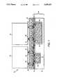
- FIG. 1depicts, in highly diagrammatic form, an integrated electronic system 20 wherein a plurality of pin-mounted memory cubes 22 are integrated with a base element 24 comprising a multi-chip high density interconnect assembly or module of the type described in the various background patents referred to hereinabove.
- the pin-mounted memory cubes 22are representative of any pinmounted component, including DIP components.
- memory cubes 22may be placed very tightly together, leaving only sufficient room for repair. Additionally, they may be potted or glued together to satisfy cooling or related requirements.
- a ceramic substrate 26has representative cavities 28 and 30 formed therein by a suitable milling process, such as laser, ultrasonic or mechanical milling. Placed and adhered within cavities 28 and 30 are a plurality of components in the representative form of individual integrated circuit chips 32 and 34 having respective upper surfaces 36 and 38 with representative chip contact pads 40 disposed thereon. Upper surfaces 36 and 38 are generally even with each other (i.e. lie in a common plane) and with an upper surface 42 of substrate 26, the substrate 26 upper surface 42 being an unmilled portion of substrate 26.
- the high density interconnect multi-chip module assembly 24is completed by an interconnect overcoat 44 which is built up as described in the various patents referred to hereinabove.
- a polyimide film 46such as Kapton polyimide, which is about 12.5 to 75 microns thick, is pre-treated to promote adhesion, and is coated on one side with a polyetherimide resin or another thermoplastic, and laminated across upper surfaces 36 and 38 of chips 32 and 34, and across the upper unmilled surface 42 of substrate 26.
- via holes 48are laser drilled in the Kapton polyimide 46 and Ultem adhesive layers in alignment with contact pads 40 on chips 32 and 34 to which it is desired to make contact.
- the diameter of HDI via hole 48may taper from 24 microns at the bottom to 50 microns at the top.
- Buildup of HDI overcoat 44continues by forming a patterned metallization layer 50 over Kapton layer 46 and extending into via holes 48 to make electrical contact with chip contact pads 40. Additional dielectric and metallization layers are provided as required (such as layers 46' and 48') in order to provide all of the desired electrical connections among chips 32 and 34, and also to provide connections, where required, with interconnect pads 52 on the upper surface 60 of HDI overcoat structure 44, which comprises a planar boundary defining the boundary of high density interconnect assembly 24.
- a mask layer 62 of polymer dielectric materialis bonded to planar surface 60 and to the interconnect pads.
- Polymer mask layer 62is approximately two to ten mils thick, and may be prepared by spin or spray coating a glue layer onto a sheet of suitable polymer material or onto planar surface 60, and then bonding the sheet of polymer material to the underlying planar surface 60 of high density interconnect assembly 24.
- polymer layer 62may comprise Kapton polyimide, the same material employed in the HDI fabrication process, but typically thicker.
- well-like via holes 64are formed by laser dithering, without use of masks, and without damage to underlying pads 52, as is generally disclosed in the above-referenced Eichelberger et al. U.S. Pat. No. 4,894,115.
- well-like via holes 64are relatively large, as discussed hereinbelow.
- Well-like via holes 64are aligned with underlying interconnection pads 52, and interconnection pads 52 are slightly larger than well-like via holes 64 to accommodate normal tolerance variations.
- Memory cubes 22(representing any pin-mounted components) have rectangular pins 66 which extend into well-like via holes 64, preferably contacting interconnect pads 52.
- a conductive polymer material 68is provided in via holes 64.
- conductive polymer material 68comprises an epoxy loaded with conductive particles, such as silver particles.
- well-like via holes 64are relatively large.
- a rectangular well-like via 64is 7 by 12 mils at the bottom, and tapers outward to 9 by 14 mils at the top.
- the resultant side slopeis approximately 80°.
- well-like via holes 64are chosen with the runout parameters of memory cube 22 pins 66 in view.
- well-like via holes 64are designed to allow ease of placement under runout conditions, as some micro-component leads are very fragile and bend easily.
- well-like via holes 64generally are elongated in one direction, particularly where adjacent memory cubes are bonded together. Under such conditions, variation in glue thicknesses bonding the individual cubes together is a more important consideration than pin-to-pin tolerance on a single component.
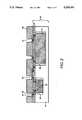
- FIG. 2depicts an intermediate step wherein polymer dielectric mask layer 62 has been applied, and well-like via holes 64 have been formed, such as by laser dithering as disclosed in U.S. Pat. No. 4,894,115.
- well-like via holes 64are dithered in place by the same laser used in other HDI processing operations; however, other methods, such as plasma milling, may be employed to form the well-like via holes by the use of an etch mask of resist or metal.
- the holesare then cleaned by a short plasma etch cycle in CF 4 O 2 or O 2 alone.
- the plasma etchremoves from underlying interconnect pads 52 any particles formed during the laser beam scanning, such as soot, any residual polymer, or any glass that may be residual from any glass removal operation performed when etching a pad mask, and cleans and roughens the interior walls of hole 64 to enhance adhesion of conductive bonding glue 68 (FIG. 1) or optional metallization.
- a suitable plasma etch techniqueis to preheat both the part and a chamber in which the part is placed, to a temperature of 110° C.
- a backsputtering stepmay be performed and an adhesion promoting layer of sputtered titanium may be applied and patterned, as epoxy does not stick well to polyimide predictively.
- FIG. 3depicts in highly-schematic form the use of pick-and-place equipment, represented by a manipulator 70, to place a sphere 72 of frozen epoxy into any one of well-like via holes 64.
- Sphere 72has a predetermined size to occupy a corresponding predetermined volume; for example, in the case of well-like via holes 64 sized as described above, frozen epoxy spheres 72 approximately 0.005 inch in diameter are employed.
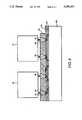
- the structure containing via holes 64appears as depicted in FIG. 4, which illustrates thawed uncured epoxy material prior to component pin insertion. As evident in FIG. 4, holes 64 are not filled to the top with uncured epoxy material 68.
- the resultant volume of uncured epoxy material 68is controlled by selection of the size of frozen epoxy spheres 72 so that holes 64 do not overflow when the component pins are later inserted. This is particularly critical since glue 68, being conductive, can cause shorts, especially as the epoxy drops in viscosity during cure. Thus well-like via holes 64 allow sufficient amounts of glue 68 to be present to yield good electrical connection to component pins, to provide mechanical integrity, and to constrain the epoxy.
- Epoxies of the type employed in the practice of the inventionare traditionally delivered either in frozen syringes having capacities ranging from 1 to 10 cc, or in sheet form.
- Sheet form epoxymore particularly comprises twelve inch square sheets, 5 to 10 mils thick, on a fiberglass carrier.
- epoxy manufacturersare requested to deliver their usual product, but in the form of frozen spheres of predetermined size.
- suitable epoxy formulationsare Ablebond® 84-1LMIS (conductive paste) and Ablefilm ECF 561-1 (conductive film), made by ABLESTIK or Collinso Dominguez, Calif.
- the HDI assembly 24, mask layer 62 and frozen epoxy spheres 72 shown in FIG. 3are warmed to approximately 25° C. (room temperature).
- the HDI assembly 24, mask layer 62 and frozen epoxy spheres 72are warmed in a vacuum oven 74, as depicted schematically in FIG. 5, while the vacuum oven is being evacuated.
- Vacuum oven 74includes a vacuum pump 76 and a heating element 78.
- a pressure differentialis created between the evacuated interior 80 (i.e., the interior generally) of vacuum oven 74 and any pockets 82 of air trapped within holes 64 below epoxy spheres 72. This pressure differential draws trapped air out of pockets 82, and epoxy flows to fill the resultant space.
- module 20is the ready for bake and cure. The cure is generally allowed to occur at a temperature in the range of 130°-150° C. for one or two hours, followed by a 170° to 200° C. post-bake cure for one-half hour. These temperatures and times are exemplary only, and of course vary with the particular epoxy which is used.
- frozen epoxymay be provided in shapes other than spheres.
- a body of uncured frozen epoxymay be provided in accordance with the shape of the hole, for example as a cylinder, the frustrum of a cone, a solid rectangle, or a trapezohedron, as the case may be.
- metallized via holes 64are relatively insensitive to pin length and epoxy path length resistivity considerations. In addition, epoxy adheres better when the well-like via holes are metallized.
- the base elementcomprises a high density interconnect assembly 24.
- the base elementmay alternatively comprise any one of a variety of structures having a generally planar boundary with interconnection pads on the boundary.
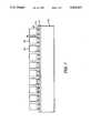
- FIG. 6depicts one such alternative, in the form of a printed circuit board 100, which optionally may have a multilayer interconnect structure 102 formed thereon, comparable to multilayer interconnect structure 44 of FIGS. 1-4.
- Multilayer interconnect structure 102either alone in combination with conductors (not shown) on printed circuit board 100, provides suitable interconnections among memory cubes 22, and additionally provides terminals 104 for external connection.
- the resultant structurecomprises a mass memory module.
- FIG. 7depicts, in highly schematic form, yet another variation of the invention, wherein the base element is a substrate 110 of ceramic or other suitable material, which may comprise an unmilled portion of the substrate of a high density interconnect assembly as described above, with a multilayer interconnect structure 112 thereover.
- a mask layer 114analogous to mask layer 62 of FIGS. 1-5, supports pins 66 of each of memory cubes 22 as described hereinabove.
Landscapes
- Engineering & Computer Science (AREA)
- Microelectronics & Electronic Packaging (AREA)
- Computer Hardware Design (AREA)
- Power Engineering (AREA)
- Manufacturing & Machinery (AREA)
- Physics & Mathematics (AREA)
- Optics & Photonics (AREA)
- Production Of Multi-Layered Print Wiring Board (AREA)
Abstract
Description
Claims (18)
Priority Applications (1)
| Application Number | Priority Date | Filing Date | Title |
|---|---|---|---|
| US07/904,719US5255431A (en) | 1992-06-26 | 1992-06-26 | Method of using frozen epoxy for placing pin-mounted components in a circuit module |
Applications Claiming Priority (1)
| Application Number | Priority Date | Filing Date | Title |
|---|---|---|---|
| US07/904,719US5255431A (en) | 1992-06-26 | 1992-06-26 | Method of using frozen epoxy for placing pin-mounted components in a circuit module |
Publications (1)
| Publication Number | Publication Date |
|---|---|
| US5255431Atrue US5255431A (en) | 1993-10-26 |
Family
ID=25419641
Family Applications (1)
| Application Number | Title | Priority Date | Filing Date |
|---|---|---|---|
| US07/904,719Expired - Fee RelatedUS5255431A (en) | 1992-06-26 | 1992-06-26 | Method of using frozen epoxy for placing pin-mounted components in a circuit module |
Country Status (1)
| Country | Link |
|---|---|
| US (1) | US5255431A (en) |
Cited By (51)
| Publication number | Priority date | Publication date | Assignee | Title |
|---|---|---|---|---|
| US5353498A (en)* | 1993-02-08 | 1994-10-11 | General Electric Company | Method for fabricating an integrated circuit module |
| US5384691A (en)* | 1993-01-08 | 1995-01-24 | General Electric Company | High density interconnect multi-chip modules including embedded distributed power supply elements |
| US5524339A (en)* | 1994-09-19 | 1996-06-11 | Martin Marietta Corporation | Method for protecting gallium arsenide mmic air bridge structures |
| US5543585A (en)* | 1994-02-02 | 1996-08-06 | International Business Machines Corporation | Direct chip attachment (DCA) with electrically conductive adhesives |
| WO1997012504A1 (en)* | 1995-09-29 | 1997-04-03 | Intel Corporation | Method for surface mounting a heatsink to a printed circuit board |
| US5740605A (en)* | 1996-07-25 | 1998-04-21 | Texas Instruments Incorporated | Bonded z-axis interface |
| US5745984A (en)* | 1995-07-10 | 1998-05-05 | Martin Marietta Corporation | Method for making an electronic module |
| US5796590A (en)* | 1996-11-05 | 1998-08-18 | Micron Electronics, Inc. | Assembly aid for mounting packaged integrated circuit devices to printed circuit boards |
| US5814174A (en)* | 1996-06-17 | 1998-09-29 | Hughes Electronics Corporation | Method for repair of metallization on circuit board substrates |
| US6005466A (en)* | 1994-07-29 | 1999-12-21 | Mitel Semiconductor Limited | Trimmable inductor structure |
| US6187652B1 (en) | 1998-09-14 | 2001-02-13 | Fujitsu Limited | Method of fabrication of multiple-layer high density substrate |
| DE19942631A1 (en)* | 1999-09-07 | 2001-03-08 | Endress Hauser Gmbh Co | Process for assembling a printed circuit board |
| US6256206B1 (en)* | 1997-12-12 | 2001-07-03 | Ela Medical S.A. | Electronic circuit for an active implantable medical device and method of manufacture |
| US20010020546A1 (en)* | 1993-11-16 | 2001-09-13 | Formfactor, Inc. | Electrical contact structures formed by configuring a flexible wire to have a springable shape and overcoating the wire with at least one layer of a resilient conductive material, methods of mounting the contact structures to electronic components, and applications for employing the contact structures |
| US6414850B1 (en) | 2000-01-11 | 2002-07-02 | Cisco Technology, Inc. | Method and apparatus for decoupling ball grid array devices |
| US20020144399A1 (en)* | 2001-04-06 | 2002-10-10 | International Business Machines Corporation | Contact column array template and method of use |
| US20020170897A1 (en)* | 2001-05-21 | 2002-11-21 | Hall Frank L. | Methods for preparing ball grid array substrates via use of a laser |
| US20020175402A1 (en)* | 2001-05-23 | 2002-11-28 | Mccormack Mark Thomas | Structure and method of embedding components in multi-layer substrates |
| US6531664B1 (en)* | 1999-04-05 | 2003-03-11 | Delphi Technologies, Inc. | Surface mount devices with solder |
| US6535398B1 (en) | 2000-03-07 | 2003-03-18 | Fujitsu Limited | Multichip module substrates with buried discrete capacitors and components and methods for making |
| US20030079896A1 (en)* | 2000-10-10 | 2003-05-01 | Matsushita Electric Industrial Co., Ltd. | Electronic component mounted member and repair method thereof |
| US6570776B2 (en)* | 2001-06-20 | 2003-05-27 | Ericsson, Inc. | Shielded electronics package structure with enhanced mechanical reliability |
| US6601295B2 (en)* | 1999-03-03 | 2003-08-05 | Mamoru Maekawa | Method of producing chip-type electronic devices |
| DE10204959A1 (en)* | 2002-02-06 | 2003-08-14 | Endress & Hauser Gmbh & Co Kg | Printed circuit board with one component |
| US20030202046A1 (en)* | 2002-04-25 | 2003-10-30 | Smida Abdelli | Orifice plate having an edge area with an aperture |
| US6657136B1 (en)* | 2000-06-30 | 2003-12-02 | Cisco Technology, Inc. | Termination board for mounting on circuit board |
| US6720500B1 (en)* | 1996-07-22 | 2004-04-13 | Honda Giken Kogyo Kabushiki Kaisha | Plug-in type electronic control unit, structure of connection of wiring board with plug member, unit of connection of electronic part with wiring board, and process for mounting electronic part |
| US20040155325A1 (en)* | 2000-10-04 | 2004-08-12 | Intel Corporation | Die-in heat spreader microelectronic package |
| US6836003B2 (en) | 1997-09-15 | 2004-12-28 | Micron Technology, Inc. | Integrated circuit package alignment feature |
| US6963143B2 (en) | 2001-08-30 | 2005-11-08 | Micron Technology, Inc. | Method of ball grid array (BGA) alignment, method of testing, alignment apparatus and semiconductor device assembly |
| US6976306B1 (en)* | 2004-07-12 | 2005-12-20 | Unitech Printed Circuit Board Corporation | Modular method for manufacturing circuit board |
| EP1062848A4 (en)* | 1998-03-12 | 2006-05-31 | Medallion Technology Llc | Integrated circuit connection using an electrically conductive adhesive |
| EP1793419A1 (en)* | 2005-12-02 | 2007-06-06 | Nederlandse Organisatie voor toegepast-natuurwetenschappelijk Onderzoek TNO | Method and system for processing frozen adhesive particles |
| US20070126445A1 (en)* | 2005-11-30 | 2007-06-07 | Micron Technology, Inc. | Integrated circuit package testing devices and methods of making and using same |
| US20070127224A1 (en)* | 2003-03-24 | 2007-06-07 | Norihito Tsukahara | Electronic circuit device and method of manufacturing the same |
| DE102006009723A1 (en)* | 2006-03-02 | 2007-09-06 | Siemens Ag | Method of making and planar contacting an electronic device and device made accordingly |
| US20070228110A1 (en)* | 1993-11-16 | 2007-10-04 | Formfactor, Inc. | Method Of Wirebonding That Utilizes A Gas Flow Within A Capillary From Which A Wire Is Played Out |
| US20080044579A1 (en)* | 2004-11-26 | 2008-02-21 | Price Matthew S | Labelling System |
| US20080142983A1 (en)* | 1999-02-24 | 2008-06-19 | Tongbi Jiang | Device having contact pad with a conductive layer and a conductive passivation layer |
| US20080264675A1 (en)* | 2007-04-25 | 2008-10-30 | Foxconn Advanced Technology Inc. | Printed circuit board and method for manufacturing the same |
| US7485562B2 (en)* | 2002-08-27 | 2009-02-03 | Micron Technology, Inc. | Method of making multichip wafer level packages and computing systems incorporating same |
| CN102648671A (en)* | 2009-12-09 | 2012-08-22 | 株式会社村田制作所 | Resin substrate with built-in electronic component and electronic circuit module |
| US8485418B2 (en) | 1995-05-26 | 2013-07-16 | Formfactor, Inc. | Method of wirebonding that utilizes a gas flow within a capillary from which a wire is played out |
| FR2996365A1 (en)* | 2012-10-03 | 2014-04-04 | Valeo Sys Controle Moteur Sas | Method for assembling connection pin with electronic board for electric car, involves depositing electrically conducting adhesive in metalized through-hole of electronic board, and inserting connection pin in through-hole |
| US9012305B1 (en)* | 2014-01-29 | 2015-04-21 | Applied Materials, Inc. | Wafer dicing using hybrid laser scribing and plasma etch approach with intermediate non-reactive post mask-opening clean |
| US9018079B1 (en)* | 2014-01-29 | 2015-04-28 | Applied Materials, Inc. | Wafer dicing using hybrid laser scribing and plasma etch approach with intermediate reactive post mask-opening clean |
| WO2015153592A1 (en)* | 2014-04-04 | 2015-10-08 | Applied Materials, Inc. | Residue removal from singulated die sidewall |
| DE102015104507A1 (en)* | 2014-12-19 | 2016-06-23 | Taiwan Semiconductor Manufacturing Co., Ltd. | Integrated fan-out structure with openings in a buffer layer |
| US9425121B2 (en) | 2013-09-11 | 2016-08-23 | Taiwan Semiconductor Manufacturing Company, Ltd. | Integrated fan-out structure with guiding trenches in buffer layer |
| US9455211B2 (en) | 2013-09-11 | 2016-09-27 | Taiwan Semiconductor Manufacturing Company, Ltd. | Integrated fan-out structure with openings in buffer layer |
| WO2017028429A1 (en)* | 2015-08-18 | 2017-02-23 | 江苏诚睿达光电有限公司 | Process method using organic silicone resin photoconverter to bond-package led by tandem rolling |
Citations (15)
| Publication number | Priority date | Publication date | Assignee | Title |
|---|---|---|---|---|
| US3749347A (en)* | 1971-09-02 | 1973-07-31 | Angstrohm Precision Inc | Mounting element for electrical components |
| US3818279A (en)* | 1973-02-08 | 1974-06-18 | Chromerics Inc | Electrical interconnection and contacting system |
| US4184043A (en)* | 1977-05-02 | 1980-01-15 | U.S. Philips Corporation | Method of providing spacers on an insulating substrate |
| US4714516A (en)* | 1986-09-26 | 1987-12-22 | General Electric Company | Method to produce via holes in polymer dielectrics for multiple electronic circuit chip packaging |
| US4721831A (en)* | 1987-01-28 | 1988-01-26 | Unisys Corporation | Module for packaging and electrically interconnecting integrated circuit chips on a porous substrate, and method of fabricating same |
| US4764485A (en)* | 1987-01-05 | 1988-08-16 | General Electric Company | Method for producing via holes in polymer dielectrics |
| US4774634A (en)* | 1986-01-21 | 1988-09-27 | Key Tronic Corporation | Printed circuit board assembly |
| US4780177A (en)* | 1988-02-05 | 1988-10-25 | General Electric Company | Excimer laser patterning of a novel resist |
| US4783695A (en)* | 1986-09-26 | 1988-11-08 | General Electric Company | Multichip integrated circuit packaging configuration and method |
| US4814944A (en)* | 1985-08-14 | 1989-03-21 | Omron Tateisi Electronics Co. | Mounting structure for surface mounted type component with projection extending down from lower surface thereof and method of mounting a surface mounted type component on a printed circuit board |
| US4835704A (en)* | 1986-12-29 | 1989-05-30 | General Electric Company | Adaptive lithography system to provide high density interconnect |
| US4842677A (en)* | 1988-02-05 | 1989-06-27 | General Electric Company | Excimer laser patterning of a novel resist using masked and maskless process steps |
| US4894115A (en)* | 1989-02-14 | 1990-01-16 | General Electric Company | Laser beam scanning method for forming via holes in polymer materials |
| US5074947A (en)* | 1989-12-18 | 1991-12-24 | Epoxy Technology, Inc. | Flip chip technology using electrically conductive polymers and dielectrics |
| US5147210A (en)* | 1988-03-03 | 1992-09-15 | Western Digital Corporation | Polymer film interconnect |
- 1992
- 1992-06-26USUS07/904,719patent/US5255431A/ennot_activeExpired - Fee Related
Patent Citations (15)
| Publication number | Priority date | Publication date | Assignee | Title |
|---|---|---|---|---|
| US3749347A (en)* | 1971-09-02 | 1973-07-31 | Angstrohm Precision Inc | Mounting element for electrical components |
| US3818279A (en)* | 1973-02-08 | 1974-06-18 | Chromerics Inc | Electrical interconnection and contacting system |
| US4184043A (en)* | 1977-05-02 | 1980-01-15 | U.S. Philips Corporation | Method of providing spacers on an insulating substrate |
| US4814944A (en)* | 1985-08-14 | 1989-03-21 | Omron Tateisi Electronics Co. | Mounting structure for surface mounted type component with projection extending down from lower surface thereof and method of mounting a surface mounted type component on a printed circuit board |
| US4774634A (en)* | 1986-01-21 | 1988-09-27 | Key Tronic Corporation | Printed circuit board assembly |
| US4783695A (en)* | 1986-09-26 | 1988-11-08 | General Electric Company | Multichip integrated circuit packaging configuration and method |
| US4714516A (en)* | 1986-09-26 | 1987-12-22 | General Electric Company | Method to produce via holes in polymer dielectrics for multiple electronic circuit chip packaging |
| US4835704A (en)* | 1986-12-29 | 1989-05-30 | General Electric Company | Adaptive lithography system to provide high density interconnect |
| US4764485A (en)* | 1987-01-05 | 1988-08-16 | General Electric Company | Method for producing via holes in polymer dielectrics |
| US4721831A (en)* | 1987-01-28 | 1988-01-26 | Unisys Corporation | Module for packaging and electrically interconnecting integrated circuit chips on a porous substrate, and method of fabricating same |
| US4780177A (en)* | 1988-02-05 | 1988-10-25 | General Electric Company | Excimer laser patterning of a novel resist |
| US4842677A (en)* | 1988-02-05 | 1989-06-27 | General Electric Company | Excimer laser patterning of a novel resist using masked and maskless process steps |
| US5147210A (en)* | 1988-03-03 | 1992-09-15 | Western Digital Corporation | Polymer film interconnect |
| US4894115A (en)* | 1989-02-14 | 1990-01-16 | General Electric Company | Laser beam scanning method for forming via holes in polymer materials |
| US5074947A (en)* | 1989-12-18 | 1991-12-24 | Epoxy Technology, Inc. | Flip chip technology using electrically conductive polymers and dielectrics |
Cited By (89)
| Publication number | Priority date | Publication date | Assignee | Title |
|---|---|---|---|---|
| US5384691A (en)* | 1993-01-08 | 1995-01-24 | General Electric Company | High density interconnect multi-chip modules including embedded distributed power supply elements |
| US5353498A (en)* | 1993-02-08 | 1994-10-11 | General Electric Company | Method for fabricating an integrated circuit module |
| US6778406B2 (en)* | 1993-11-16 | 2004-08-17 | Formfactor, Inc. | Resilient contact structures for interconnecting electronic devices |
| US6835898B2 (en) | 1993-11-16 | 2004-12-28 | Formfactor, Inc. | Electrical contact structures formed by configuring a flexible wire to have a springable shape and overcoating the wire with at least one layer of a resilient conductive material, methods of mounting the contact structures to electronic components, and applications for employing the contact structures |
| US20070228110A1 (en)* | 1993-11-16 | 2007-10-04 | Formfactor, Inc. | Method Of Wirebonding That Utilizes A Gas Flow Within A Capillary From Which A Wire Is Played Out |
| US20020117330A1 (en)* | 1993-11-16 | 2002-08-29 | Formfactor, Inc. | Resilient contact structures formed and then attached to a substrate |
| US7225538B2 (en) | 1993-11-16 | 2007-06-05 | Formfactor, Inc. | Resilient contact structures formed and then attached to a substrate |
| US20010020546A1 (en)* | 1993-11-16 | 2001-09-13 | Formfactor, Inc. | Electrical contact structures formed by configuring a flexible wire to have a springable shape and overcoating the wire with at least one layer of a resilient conductive material, methods of mounting the contact structures to electronic components, and applications for employing the contact structures |
| US5543585A (en)* | 1994-02-02 | 1996-08-06 | International Business Machines Corporation | Direct chip attachment (DCA) with electrically conductive adhesives |
| US6005466A (en)* | 1994-07-29 | 1999-12-21 | Mitel Semiconductor Limited | Trimmable inductor structure |
| US5524339A (en)* | 1994-09-19 | 1996-06-11 | Martin Marietta Corporation | Method for protecting gallium arsenide mmic air bridge structures |
| US8485418B2 (en) | 1995-05-26 | 2013-07-16 | Formfactor, Inc. | Method of wirebonding that utilizes a gas flow within a capillary from which a wire is played out |
| US5745984A (en)* | 1995-07-10 | 1998-05-05 | Martin Marietta Corporation | Method for making an electronic module |
| WO1997012504A1 (en)* | 1995-09-29 | 1997-04-03 | Intel Corporation | Method for surface mounting a heatsink to a printed circuit board |
| US5779134A (en)* | 1995-09-29 | 1998-07-14 | Intel Corporation | Method for surface mounting a heatsink to a printed circuit board |
| US5814174A (en)* | 1996-06-17 | 1998-09-29 | Hughes Electronics Corporation | Method for repair of metallization on circuit board substrates |
| US6720500B1 (en)* | 1996-07-22 | 2004-04-13 | Honda Giken Kogyo Kabushiki Kaisha | Plug-in type electronic control unit, structure of connection of wiring board with plug member, unit of connection of electronic part with wiring board, and process for mounting electronic part |
| US5740605A (en)* | 1996-07-25 | 1998-04-21 | Texas Instruments Incorporated | Bonded z-axis interface |
| US5796590A (en)* | 1996-11-05 | 1998-08-18 | Micron Electronics, Inc. | Assembly aid for mounting packaged integrated circuit devices to printed circuit boards |
| US6858453B1 (en) | 1997-09-15 | 2005-02-22 | Micron Technology, Inc. | Integrated circuit package alignment feature |
| US6836003B2 (en) | 1997-09-15 | 2004-12-28 | Micron Technology, Inc. | Integrated circuit package alignment feature |
| US6256206B1 (en)* | 1997-12-12 | 2001-07-03 | Ela Medical S.A. | Electronic circuit for an active implantable medical device and method of manufacture |
| EP1062848A4 (en)* | 1998-03-12 | 2006-05-31 | Medallion Technology Llc | Integrated circuit connection using an electrically conductive adhesive |
| US6187652B1 (en) | 1998-09-14 | 2001-02-13 | Fujitsu Limited | Method of fabrication of multiple-layer high density substrate |
| US20080142983A1 (en)* | 1999-02-24 | 2008-06-19 | Tongbi Jiang | Device having contact pad with a conductive layer and a conductive passivation layer |
| US6601295B2 (en)* | 1999-03-03 | 2003-08-05 | Mamoru Maekawa | Method of producing chip-type electronic devices |
| US6531664B1 (en)* | 1999-04-05 | 2003-03-11 | Delphi Technologies, Inc. | Surface mount devices with solder |
| DE19942631A1 (en)* | 1999-09-07 | 2001-03-08 | Endress Hauser Gmbh Co | Process for assembling a printed circuit board |
| EP1083778A1 (en)* | 1999-09-07 | 2001-03-14 | Endress + Hauser GmbH + Co. | Process for mounting components on a printed circuit board |
| US6414850B1 (en) | 2000-01-11 | 2002-07-02 | Cisco Technology, Inc. | Method and apparatus for decoupling ball grid array devices |
| US6535398B1 (en) | 2000-03-07 | 2003-03-18 | Fujitsu Limited | Multichip module substrates with buried discrete capacitors and components and methods for making |
| US6657136B1 (en)* | 2000-06-30 | 2003-12-02 | Cisco Technology, Inc. | Termination board for mounting on circuit board |
| US20040155325A1 (en)* | 2000-10-04 | 2004-08-12 | Intel Corporation | Die-in heat spreader microelectronic package |
| US20030079896A1 (en)* | 2000-10-10 | 2003-05-01 | Matsushita Electric Industrial Co., Ltd. | Electronic component mounted member and repair method thereof |
| US6675474B2 (en)* | 2000-10-10 | 2004-01-13 | Matsushita Electric Industrial Co., Ltd. | Electronic component mounted member and repair method thereof |
| US6968614B2 (en)* | 2001-04-06 | 2005-11-29 | International Business Machines Corporation | Method for positioning an electronic module having a contact column array into a template |
| US20020144399A1 (en)* | 2001-04-06 | 2002-10-10 | International Business Machines Corporation | Contact column array template and method of use |
| US20020170897A1 (en)* | 2001-05-21 | 2002-11-21 | Hall Frank L. | Methods for preparing ball grid array substrates via use of a laser |
| US20050170658A1 (en)* | 2001-05-21 | 2005-08-04 | Hall Frank L. | Methods for preparing ball grid array substrates via use of a laser |
| US20040169024A1 (en)* | 2001-05-21 | 2004-09-02 | Hall Frank L. | Methods for preparing ball grid array substrates via use of a laser |
| US20060249494A1 (en)* | 2001-05-21 | 2006-11-09 | Hall Frank L | Methods for preparing ball grid array substrates via use of a laser |
| US20040104206A1 (en)* | 2001-05-21 | 2004-06-03 | Hall Frank L. | Methods for preparing ball grid array substrates via use of a laser |
| US20060249495A1 (en)* | 2001-05-21 | 2006-11-09 | Hall Frank L | Methods for preparing ball grid array substrates via use of a laser |
| US20060249492A1 (en)* | 2001-05-21 | 2006-11-09 | Hall Frank L | Methods for preparing ball grid array substrates via use of a laser |
| US20060163573A1 (en)* | 2001-05-21 | 2006-07-27 | Hall Frank L | Method for preparing ball grid array substrates via use of a laser |
| US20060249493A1 (en)* | 2001-05-21 | 2006-11-09 | Hall Frank L | Methods for preparing ball grid array substrates via use of a laser |
| US20020175402A1 (en)* | 2001-05-23 | 2002-11-28 | Mccormack Mark Thomas | Structure and method of embedding components in multi-layer substrates |
| US6570776B2 (en)* | 2001-06-20 | 2003-05-27 | Ericsson, Inc. | Shielded electronics package structure with enhanced mechanical reliability |
| US6991960B2 (en) | 2001-08-30 | 2006-01-31 | Micron Technology, Inc. | Method of semiconductor device package alignment and method of testing |
| US7005754B2 (en) | 2001-08-30 | 2006-02-28 | Micron Technology, Inc. | Method of ball grid array (BGA) alignment, method of testing, alignment apparatus and semiconductor device assembly |
| US6963143B2 (en) | 2001-08-30 | 2005-11-08 | Micron Technology, Inc. | Method of ball grid array (BGA) alignment, method of testing, alignment apparatus and semiconductor device assembly |
| DE10204959A1 (en)* | 2002-02-06 | 2003-08-14 | Endress & Hauser Gmbh & Co Kg | Printed circuit board with one component |
| US20030202046A1 (en)* | 2002-04-25 | 2003-10-30 | Smida Abdelli | Orifice plate having an edge area with an aperture |
| US7485562B2 (en)* | 2002-08-27 | 2009-02-03 | Micron Technology, Inc. | Method of making multichip wafer level packages and computing systems incorporating same |
| US20070127224A1 (en)* | 2003-03-24 | 2007-06-07 | Norihito Tsukahara | Electronic circuit device and method of manufacturing the same |
| US6976306B1 (en)* | 2004-07-12 | 2005-12-20 | Unitech Printed Circuit Board Corporation | Modular method for manufacturing circuit board |
| US20060005382A1 (en)* | 2004-07-12 | 2006-01-12 | Unitech Printed Circuit Board Corporation | Modular method for manufacturing circuit board |
| US20080044579A1 (en)* | 2004-11-26 | 2008-02-21 | Price Matthew S | Labelling System |
| US20070126445A1 (en)* | 2005-11-30 | 2007-06-07 | Micron Technology, Inc. | Integrated circuit package testing devices and methods of making and using same |
| US8236377B2 (en) | 2005-12-02 | 2012-08-07 | Nederlandse Organisatie Voor Toegepast-Natuurwetenschappelijk Onderzoek Tno | Method and system for processing frozen adhesive particles |
| EP1793419A1 (en)* | 2005-12-02 | 2007-06-06 | Nederlandse Organisatie voor toegepast-natuurwetenschappelijk Onderzoek TNO | Method and system for processing frozen adhesive particles |
| US20100189892A1 (en)* | 2005-12-02 | 2010-07-29 | Erik Christian Nicolaas Puik | Method and system for processing frozen adhesive particles |
| WO2007064204A3 (en)* | 2005-12-02 | 2007-07-26 | Tno | Method and system for processing frozen adhesive particles |
| US20090026602A1 (en)* | 2006-03-02 | 2009-01-29 | Siemens Aktiengesellschaft | Method For Manufacturing And Making Planar Contact With An Electronic Apparatus, And Correspondingly Manufactured Apparatus |
| DE102006009723A1 (en)* | 2006-03-02 | 2007-09-06 | Siemens Ag | Method of making and planar contacting an electronic device and device made accordingly |
| US8642465B2 (en) | 2006-03-02 | 2014-02-04 | Siemens Aktiengesellschaft | Method for manufacturing and making planar contact with an electronic apparatus, and correspondingly manufactured apparatus |
| US20080264675A1 (en)* | 2007-04-25 | 2008-10-30 | Foxconn Advanced Technology Inc. | Printed circuit board and method for manufacturing the same |
| CN102648671A (en)* | 2009-12-09 | 2012-08-22 | 株式会社村田制作所 | Resin substrate with built-in electronic component and electronic circuit module |
| US20120236508A1 (en)* | 2009-12-09 | 2012-09-20 | Murata Manufacturing Co., Ltd. | Electronic-component embedded resin substrate and electronic circuit module |
| FR2996365A1 (en)* | 2012-10-03 | 2014-04-04 | Valeo Sys Controle Moteur Sas | Method for assembling connection pin with electronic board for electric car, involves depositing electrically conducting adhesive in metalized through-hole of electronic board, and inserting connection pin in through-hole |
| US9425121B2 (en) | 2013-09-11 | 2016-08-23 | Taiwan Semiconductor Manufacturing Company, Ltd. | Integrated fan-out structure with guiding trenches in buffer layer |
| US10083946B2 (en) | 2013-09-11 | 2018-09-25 | Taiwan Semiconductor Manufacturing Company, Ltd. | Integrated fan-out structure with guiding trenches in buffer layer |
| US10354982B2 (en) | 2013-09-11 | 2019-07-16 | Taiwan Semiconductor Manufacturing Company, Ltd. | Integrated fan-out structure with guiding trenches in buffer layer |
| US9799581B2 (en) | 2013-09-11 | 2017-10-24 | Taiwan Semiconductor Manufacturing Company, Ltd. | Integrated fan-out structure with openings in buffer layer |
| US9633895B2 (en) | 2013-09-11 | 2017-04-25 | Taiwan Semiconductor Manufacturing Company, Ltd. | Integrated fan-out structure with guiding trenches in buffer layer |
| US9455211B2 (en) | 2013-09-11 | 2016-09-27 | Taiwan Semiconductor Manufacturing Company, Ltd. | Integrated fan-out structure with openings in buffer layer |
| WO2015116378A1 (en)* | 2014-01-29 | 2015-08-06 | Applied Materials, Inc. | Wafer dicing using hybrid laser scribing and plasma etch approach with intermediate non-reactive post mask-opening clean |
| US9012305B1 (en)* | 2014-01-29 | 2015-04-21 | Applied Materials, Inc. | Wafer dicing using hybrid laser scribing and plasma etch approach with intermediate non-reactive post mask-opening clean |
| TWI644353B (en)* | 2014-01-29 | 2018-12-11 | 應用材料股份有限公司 | Wafer dicing using hybrid laser scribing and plasma etch approach with intermediate reactive post mask-opening clean |
| WO2015116457A1 (en)* | 2014-01-29 | 2015-08-06 | Applied Materials, Inc. | Wafer dicing using hybrid laser scribing and plasma etch approach with intermediate reactive post mask-opening clean |
| TWI635570B (en)* | 2014-01-29 | 2018-09-11 | 應用材料股份有限公司 | Wafer dicing using hybrid laser scribing and plasma etch approach with intermediate non-reactive post mask-opening clean |
| US9018079B1 (en)* | 2014-01-29 | 2015-04-28 | Applied Materials, Inc. | Wafer dicing using hybrid laser scribing and plasma etch approach with intermediate reactive post mask-opening clean |
| WO2015153592A1 (en)* | 2014-04-04 | 2015-10-08 | Applied Materials, Inc. | Residue removal from singulated die sidewall |
| DE102015104507A1 (en)* | 2014-12-19 | 2016-06-23 | Taiwan Semiconductor Manufacturing Co., Ltd. | Integrated fan-out structure with openings in a buffer layer |
| DE102015104507B4 (en) | 2014-12-19 | 2022-06-30 | Taiwan Semiconductor Manufacturing Co., Ltd. | Integrated fan-out structure with openings in a buffer layer and its manufacturing process |
| WO2017028429A1 (en)* | 2015-08-18 | 2017-02-23 | 江苏诚睿达光电有限公司 | Process method using organic silicone resin photoconverter to bond-package led by tandem rolling |
| US10141486B2 (en) | 2015-08-18 | 2018-11-27 | Jiangsu Cherrity Optronics Co., Ltd. | Process method using organic silicone resin photoconverter to bond-package LED by tandem rolling |
| JP2018525816A (en)* | 2015-08-18 | 2018-09-06 | ジアンスー チェリティ オプトロニクス カンパニー リミテッドJiangsu Cherrity Optronics Co., Ltd. | Process method for packaging by bonding LEDs with an organic silicon resin light converter by serial rolling |
| CN106469780A (en)* | 2015-08-18 | 2017-03-01 | 江苏诚睿达光电有限公司 | A kind of process of the organic siliconresin light conversion body laminating encapsulation LED based on series connection rolling |
Similar Documents
| Publication | Publication Date | Title |
|---|---|---|
| US5255431A (en) | Method of using frozen epoxy for placing pin-mounted components in a circuit module | |
| US5744758A (en) | Multilayer circuit board and process of production thereof | |
| US6256206B1 (en) | Electronic circuit for an active implantable medical device and method of manufacture | |
| US5677575A (en) | Semiconductor package having semiconductor chip mounted on board in face-down relation | |
| US6271056B1 (en) | Stacked semiconductor package and method of fabrication | |
| KR100865426B1 (en) | Semiconductor device and manufacturing method thereof | |
| KR100687976B1 (en) | Method for manufacturing an electronic module and an electronic module | |
| US7422978B2 (en) | Methods of manufacturing interposers with flexible solder pad elements | |
| US6798070B2 (en) | Electronic device assembly and a method of connecting electronic devices constituting the same | |
| US5784780A (en) | Method of mounting a flip-chip | |
| US6544428B1 (en) | Method for producing a multi-layer circuit board using anisotropic electro-conductive adhesive layer | |
| US20030057544A1 (en) | Integrated assembly protocol | |
| US7376318B2 (en) | Circuit board and its manufacturing method | |
| US5636104A (en) | Printed circuit board having solder ball mounting groove pads and a ball grid array package using such a board | |
| US20030059976A1 (en) | Integrated package and methods for making same | |
| JPH04251969A (en) | Electronic device | |
| KR20040047902A (en) | Semiconductor device and method of manufacturing the same | |
| WO1999044401A1 (en) | Stacking layers containing enclosed ic chips | |
| JPH1070362A (en) | Method and structure for coupling board | |
| JPH04233264A (en) | Compact high-density connection structure | |
| WO1997022146A1 (en) | Semiconductor package with multilayered circuit and semiconductor device | |
| US7663254B2 (en) | Semiconductor apparatus and method of manufacturing the same | |
| JP2001015650A (en) | Ball grid array package and its manufacture | |
| US6739046B1 (en) | Method for producing dendrite interconnect for planarization | |
| US6880244B2 (en) | Circuit board having simultaneously and unitarily formed wiring patterns and protrusions |
Legal Events
| Date | Code | Title | Description |
|---|---|---|---|
| AS | Assignment | Owner name:GENERAL ELECTRIC COMPANY, A CORP. OF NY Free format text:ASSIGNMENT OF ASSIGNORS INTEREST.;ASSIGNOR:BURDICK, WILLIAM E.;REEL/FRAME:006178/0013 Effective date:19920622 | |
| FEPP | Fee payment procedure | Free format text:PAYOR NUMBER ASSIGNED (ORIGINAL EVENT CODE: ASPN); ENTITY STATUS OF PATENT OWNER: LARGE ENTITY | |
| AS | Assignment | Owner name:MARTIN MARIETTA CORPORATION, MARYLAND Free format text:ASSIGNMENT OF ASSIGNORS INTEREST;ASSIGNOR:GENERAL ELECTRIC COMPANY;REEL/FRAME:007046/0736 Effective date:19940322 | |
| REMI | Maintenance fee reminder mailed | ||
| AS | Assignment | Owner name:LOCKHEED MARTIN CORPORATION, MARYLAND Free format text:ASSIGNMENT OF ASSIGNORS INTEREST;ASSIGNOR:MARTIN MARIETTA CORPORATION;REEL/FRAME:008628/0518 Effective date:19960128 | |
| LAPS | Lapse for failure to pay maintenance fees | ||
| FP | Lapsed due to failure to pay maintenance fee | Effective date:19971029 | |
| FEPP | Fee payment procedure | Free format text:PAYER NUMBER DE-ASSIGNED (ORIGINAL EVENT CODE: RMPN); ENTITY STATUS OF PATENT OWNER: LARGE ENTITY Free format text:PAYOR NUMBER ASSIGNED (ORIGINAL EVENT CODE: ASPN); ENTITY STATUS OF PATENT OWNER: LARGE ENTITY | |
| STCH | Information on status: patent discontinuation | Free format text:PATENT EXPIRED DUE TO NONPAYMENT OF MAINTENANCE FEES UNDER 37 CFR 1.362 |