US5255203A - Interconnect structure for programmable logic device - Google Patents
Interconnect structure for programmable logic deviceDownload PDFInfo
- Publication number
- US5255203A US5255203AUS07/538,211US53821190AUS5255203AUS 5255203 AUS5255203 AUS 5255203AUS 53821190 AUS53821190 AUS 53821190AUS 5255203 AUS5255203 AUS 5255203A
- Authority
- US
- United States
- Prior art keywords
- horizontal
- vertical
- interconnect
- bus
- input
- Prior art date
- Legal status (The legal status is an assumption and is not a legal conclusion. Google has not performed a legal analysis and makes no representation as to the accuracy of the status listed.)
- Expired - Fee Related
Links
Images


Classifications
- H—ELECTRICITY
- H03—ELECTRONIC CIRCUITRY
- H03K—PULSE TECHNIQUE
- H03K19/00—Logic circuits, i.e. having at least two inputs acting on one output; Inverting circuits
- H03K19/02—Logic circuits, i.e. having at least two inputs acting on one output; Inverting circuits using specified components
- H03K19/173—Logic circuits, i.e. having at least two inputs acting on one output; Inverting circuits using specified components using elementary logic circuits as components
- H03K19/177—Logic circuits, i.e. having at least two inputs acting on one output; Inverting circuits using specified components using elementary logic circuits as components arranged in matrix form
- H03K19/17736—Structural details of routing resources
- H—ELECTRICITY
- H03—ELECTRONIC CIRCUITRY
- H03K—PULSE TECHNIQUE
- H03K19/00—Logic circuits, i.e. having at least two inputs acting on one output; Inverting circuits
- H03K19/02—Logic circuits, i.e. having at least two inputs acting on one output; Inverting circuits using specified components
- H03K19/173—Logic circuits, i.e. having at least two inputs acting on one output; Inverting circuits using specified components using elementary logic circuits as components
- H03K19/177—Logic circuits, i.e. having at least two inputs acting on one output; Inverting circuits using specified components using elementary logic circuits as components arranged in matrix form
- H03K19/17704—Logic circuits, i.e. having at least two inputs acting on one output; Inverting circuits using specified components using elementary logic circuits as components arranged in matrix form the logic functions being realised by the interconnection of rows and columns
- H—ELECTRICITY
- H03—ELECTRONIC CIRCUITRY
- H03K—PULSE TECHNIQUE
- H03K19/00—Logic circuits, i.e. having at least two inputs acting on one output; Inverting circuits
- H03K19/02—Logic circuits, i.e. having at least two inputs acting on one output; Inverting circuits using specified components
- H03K19/173—Logic circuits, i.e. having at least two inputs acting on one output; Inverting circuits using specified components using elementary logic circuits as components
- H03K19/177—Logic circuits, i.e. having at least two inputs acting on one output; Inverting circuits using specified components using elementary logic circuits as components arranged in matrix form
- H03K19/17724—Structural details of logic blocks
- H03K19/17728—Reconfigurable logic blocks, e.g. lookup tables
- H—ELECTRICITY
- H03—ELECTRONIC CIRCUITRY
- H03K—PULSE TECHNIQUE
- H03K19/00—Logic circuits, i.e. having at least two inputs acting on one output; Inverting circuits
- H03K19/02—Logic circuits, i.e. having at least two inputs acting on one output; Inverting circuits using specified components
- H03K19/173—Logic circuits, i.e. having at least two inputs acting on one output; Inverting circuits using specified components using elementary logic circuits as components
- H03K19/177—Logic circuits, i.e. having at least two inputs acting on one output; Inverting circuits using specified components using elementary logic circuits as components arranged in matrix form
- H03K19/17736—Structural details of routing resources
- H03K19/17744—Structural details of routing resources for input/output signals
- H—ELECTRICITY
- H03—ELECTRONIC CIRCUITRY
- H03K—PULSE TECHNIQUE
- H03K19/00—Logic circuits, i.e. having at least two inputs acting on one output; Inverting circuits
- H03K19/02—Logic circuits, i.e. having at least two inputs acting on one output; Inverting circuits using specified components
- H03K19/173—Logic circuits, i.e. having at least two inputs acting on one output; Inverting circuits using specified components using elementary logic circuits as components
- H03K19/177—Logic circuits, i.e. having at least two inputs acting on one output; Inverting circuits using specified components using elementary logic circuits as components arranged in matrix form
- H03K19/1778—Structural details for adapting physical parameters
- H03K19/17792—Structural details for adapting physical parameters for operating speed
Definitions
- the present inventionrelates generally to programmable logic devices and, more particularly, to programmable gate arrays consisting of an array of logic blocks and input/output blocks with a configurable interconnection structure.
- the programmable gate arrayis a high performance, user programmable device containing three types of configurable elements that are customized to a user system design.
- the three elementsare (1) an array of configurable logic blocks (CLBs), (2) with input/output blocks (IOBs) around a perimeter, all linked by (3) a flexible programmable interconnect network.
- CLBsconfigurable logic blocks
- IOBsinput/output blocks
- the system design desired by a useris implemented in the device by configuring programmable RAM cells. These RAM cells control the logic functionality performed by the CLBs, IOBs and the interconnect.
- the configurationis implemented using PGA design software tools.
- Xilinxoriginally introduced the XC2000 series of logic cell arrays and has more recently introduced a second generation XC3000 family of integrated circuit programmable gate arrays.
- a description of the 2000 series, as well as related programmable logic device art,can be found in THE PROGRAMMABLE GATE ARRAY DESIGN HANDBOOK, First Edition, published by Xilinx, pages 1-1 through 1-31.
- the architecture for the XC3000 familyis provided in a technical data handbook published by Xilinx entitled XC3000 LOGIC CELL ARRAY FAMILY, pages 1-31.
- Each of these Xilinx publicationsis incorporated by reference in this application as providing a description of the prior art.
- the programmable gate arrayconsists of a configurable interconnect, a ring of configurable input/output blocks, and an array of configurable logic blocks. It is the combination of these three major features that provides flexibility and data processing power for programmable gate arrays.
- the programmable gate arrays of the prior artsuffer certain limitations in the interconnect structure.
- the configurable interconnect structuremust provide the ability to form networks on the programmable gate array which optimize utilization of the resources on the chip.
- the prior art interconnect systemshave tended to force connection in the logical network to configurable blocks in a relatively small area. For instance, a prior system provides direct connections only between adjacent configurable logic blocks.
- the inputs and outputs on the configurable logic blocksare arranged in a left to right or otherwise asymmetrical layout that forces signal flow in a certain direction across the chip. This causes congestion on the interconnect structure for applications requiring a large number of inputs or outputs. Also, this forces the printed circuit board layout, which includes one of these asymmetrically designed logic cell arrays, to provide for inputs on one side of the logic cell array and outputs on the other.
- the present inventionprovides an architecture for a configurable logic array with an interconnect structure which improves flexibility in creating networks to allow for greater utilization of the configurable logic blocks and input/output blocks on the device.
- the present inventionprovides a configurable interconnect structure for a logic device, such as a programmable gate array.
- the configurable interconnect structureincludes a configuration store, storing program data specifying a user defined interconnect function.
- a plurality of horizontal buses and vertical busesare included along the rows and columns of the logic array cells.
- Programmable switching elementsare included at the intersections of the horizontal and vertical buses for interconnecting the horizontal and vertical buses in response to program data.
- the horizontal buses and the vertical busesinclude bidirectional, general interconnect (BGI) segments, which extend along a respective horizontal or vertical bus from the intersection of one of the crossing buses to the intersection of another of the crossing buses.
- BGIgeneral interconnect
- Each of the BGI segmentsis connected to a plurality of programmable interconnect points for interconnecting respective inputs or outputs of logic cells and input/output cells in the array with the respective BGI segment. Also, each BGI segment is connected to the switching means at the intersections with crossing buses to allow for connection to other BGI segments in response to the program data.
- the busesalso include long lines which extend across the array, each connected to programmable interconnect points for interconnecting outputs of logic cells and input/output cells in response to program data in the configuration store, and each connected directly to a plurality of inputs to the logic cells or input/output cells.
- the busesinclude uncommitted long lines which do not have direct connections to inputs of input/output cells or logic cells, but have programmable connections to intersecting buses at the switching means and to outputs of the logic cells and input/output cells.
- the present inventionprovides a plurality of programmable interconnect means at the intersections of horizontal and vertical buses for interconnecting in response to program data in the configuration store a respective horizontal (BGI) segment and vertical long line, or a respective vertical (BGI) segment and a horizontal long line.
- FIG. 1is schematic diagram illustrating the layout of the programmable gate array according to the present invention.
- FIG. 2is a schematic diagram of the configuration memory in the programmable gate array according to the present invention.
- FIG. 3is a diagram of the configuration memory storage cell.
- FIG. 4illustrates a notation scheme for vertical buses in the programmable gate array.
- FIG. 5illustrates a notation scheme for the horizontal buses in the programmable gate array.
- FIG. 6illustrates the placement of the switch matrices in lines 5-14 of the horizontal and vertical buses in the programmable gate array.
- FIG. 7illustrates the intersection of a vertical bus with a horizontal bus.
- FIG. 8illustrates an alternative intersection of a vertical bus with a horizontal.
- FIG. 9illustrates the intersection of vertical buses 1 and 9 with even numbered horizontal buses and horizontal buses 1 and 9 with even numbered vertical buses.
- FIG. 10illustrates the intersection of vertical buses 1 and 9 with the odd numbered horizontal buses and horizontal buses 1 and 9 with the odd numbered vertical buses.
- FIG. 11illustrates the intersection of horizontal bus 1 with vertical bus 1 at the corner.
- FIG. 12illustrates the intersection of horizontal bus 1 with vertical bus 9 at the corner.
- FIG. 13illustrates the intersection of horizontal bus 9 with vertical bus 1 at the corner.
- FIG. 14illustrates the intersection of horizontal bus 9 with vertical bus 9 at the corner.
- FIG. 14Aillustrates an alternative corner connection scheme that can be used at all four corner intersections, replacing the schemes of FIGS. 11-14.
- FIG. 15illustrates the connection of lines 16 and 17 of the vertical buses with the global reset and global clock buffers.
- FIG. 15Aillustrates the connection of the vertical lines 16 and 17 with the configurable logic blocks.
- FIG. 15Billustrates the signal path from an input/output pad bypassing internal IOB logic for connection to the global clock buffer, horizontal alternate buffer or vertical alternate buffer.
- FIG. 15Cillustrates the inputs to the global clock buffer.
- FIG. 16illustrates the connection of the horizontal alternate buffers with line 15 on the horizontal buses and the vertical alternate buffers with line 15 on the vertical buses.
- FIG. 16Aillustrates the connection of the input/output blocks and the configurable logic blocks with line 15.
- FIG. 16Billustrates the input paths to the vertical alternate buffer.
- FIG. 16Cillustrates the input paths to the horizontal alternate buffer.
- FIG. 16Dillustrates the crystal oscillator circuit by which the oscillator signal OSC is generated on the chip.
- FIG. 16Eillustrates the external connections for the oscillator of FIG. 16D.
- FIG. 17illustrates one implementation of a programmable interconnect point using bidirectional pass transistors.
- FIG. 18illustrates an alternative configuration of a programmable interconnect point using a unidirectional multiplexer technique.
- FIG. 19illustrates the interconnect structure of the switch matrix.
- FIG. 20illustrates the repowering buffer used in the programmable interconnect.
- FIG. 21shows the switch matrix interconnection options for each connection to the switch matrix.
- FIG. 22illustrates the interconnection in the segment boxes on vertical buses 1 and 9.
- FIG. 23illustrates the interconnection in the segment boxes on horizontal buses 1 and 9.
- FIG. 24illustrates the segment box interconnection options for each connection to the segment box.
- FIG. 25is an overview block diagram of the configurable logic block.
- FIG. 26schematically illustrates the inputs and outputs and provides a notation for the configurable logic block.
- FIG. 27illustrates the inputs and outputs of the complex input/output block.
- FIG. 28illustrates the inputs and outputs of the simple input/output block.
- FIG. 29illustrates the direct connections from outputs of next adjacent configurable logic blocks to the inputs of a given logic block.
- FIG. 30illustrates direct connections from adjacent configurable logic blocks to the inputs of the center configurable logic block.
- FIG. 31illustrates direct connections from the output of the center configurable logic block to adjacent and next adjacent configurable logic blocks.
- FIG. 32illustrates direct connection of the outputs X1-X4, on peripheral configurable logic blocks.
- FIG. 33illustrates direct connection to the inputs of a peripheral configurable logic block.
- FIG. 34illustrates direct connections to the inputs F1-F4 on a peripheral configurable logic block.
- FIG. 35illustrates the programmable connections between the interconnect structure and the configurable logic blocks.
- FIG. 36illustrates the fixed connections between the interconnect structure and the configurable logic blocks.
- FIG. 37illustrates the programmable connection of the configurable logic blocks in the array to uncommitted long lines.
- FIG. 38illustrates the programmable connections to the outer long lines from the CLBs.
- FIG. 39illustrates the reach between input/output blocks and configurable logic blocks on long lines.
- FIG. 40illustrates the programmable connections between the input/output blocks on the top side of the configurable array and horizontal bus 1.
- FIG. 41illustrates the programmable connections between horizontal bus 9 and the input/output blocks on the bottom side of the configurable array.
- FIG. 42illustrates the programmable interconnects between the vertical bus 1 and the input/output blocks on the left side of the array.
- FIG. 43illustrates the programmable interconnects between vertical bus 9 and the input/output blocks on the right side of the array.
- FIG. 44illustrates the connection of the clock and reset signals to the complex input/output blocks, as well as the programmable connections of the inputs and the outputs of the input/output blocks on the top side of the array to the vertical buses.
- FIG. 45illustrates the connection of the clock and reset signals to the input/output blocks on the bottom side of the array, and connection of these bottom side input/output blocks to the vertical buses.
- FIG. 46illustrates the connection of the clock and reset signals to the input/output blocks on the left side, and connection of these left side input/output blocks to horizontal buses.
- FIG. 47illustrates the connection of the clock and the reset signals to the input/output blocks on the right side of the array, and connection of these right side input/output blocks to the horizontal buses.
- FIG. 48illustrates the connection of the control signal inputs on the input/output blocks on the top and left side of the array to the adjacent interconnect buses.
- FIG. 49illustrates the connection of the control signal inputs to the input/output blocks on the right and bottom side of the array to the adjacent interconnect buses.
- FIGS. 1-3the basic layout and programming structure of the programmable gate array is described.
- FIGS. 4-24a detailed description of the interconnect structure is set out with reference to FIGS. 4-24. This is followed by a description of the connections among the configurable logic blocks, input/output cells and the interconnect structure with reference to FIGS. 25-39.
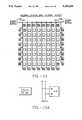
- FIG. 1illustrates the layout of the programmable gate array according to the present invention. Also provided in FIG. 1 is a notation which is utilized to describe the programmable gate array in this application. Accordingly, the programmable gate array shown in FIG. 1 consists of an array of configurable logic blocks illustrated by the square symbol with bold lines shown at the upper left hand corner of the figure. Each configurable logic block in the array is labeled With a row and column number, i.e. in the upper left hand corner of the array, the configurable logic blocks are labeled R1C1, R1C2, and so on until the lower right hand corner of the array where the configurable logic block is labeled R8C8.
- Pads 2-13, 16-27, 29-40, 43-54, 57-68, 71-82, 85-96 and 99-110are coupled to configurable input/output blocks represented by the symbol shown in the upper left hand corner of the figure.
- Pads 1, 14, 15, 28, 41, 42, 55, 56, 69, 70, 83, 84, 79 and 98are utilized for functions other than configurable input/output blocks, such as power, ground, global clock and reset signal inputs, and programming mode control signals.
- the connection of these miscellaneous padsis similar to that done in prior art programmable gate array and is not further described here.
- the interconnect structureconsists of nine horizontal buses labeled HBUS1 through HBUS9 with nine intersecting vertical buses VBUS1 through VBUS9.
- the intersections of vertical bus 1 and vertical bus 9 with the horizontal buses 2-8are characterized by having segment boxes which provide programmable interconnection between the respective horizontal bus and the vertical bus as described in detail below.
- the intersections of horizontal bus 1 and horizontal bus 9 with vertical buses 2-8are characterized by segment boxes providing the programmable interconnection between the horizontal and vertical buses.
- intersections of the vertical buses 2-8 with the horizontal buses 2-8are characterized by switching matrices providing for interconnection between the respective horizontal and vertical buses.
- the placement of the segment boxes and switching matricesis schematically illustrated in FIG. 1 using the symbols illustrated in the lower left hand corner of the figure. The detailed structure of the switching matrices and segment boxes is described below.
- the programmable gate array according to the present inventioncontains three types of configurable elements that are customized to a user system design which is specified in a configuration memory.
- the three configurable elementsare the array of configurable logic blocks (CLBs), the configurable input/output blocks (IOBs) around the perimeter, and the programmable interconnect network.
- CLBsconfigurable logic blocks
- IOBsconfigurable input/output blocks
- the system design of a useris implemented in the programmable gate array by configuring programmable RAM cells known as a configuration memory. These RAM cells control the logic functionality performed by the CLBs, IOBs, and the interconnect.
- the loading of the configuration memoryis implemented using a set of design software tools as well known in the art.
- the perimeter of configurable IOBsprovide a programmable interface between the internal logic array and device package pins.
- the array of CLBsperform user specified logic functions.
- the interconnectionconsists of direct connections between specific CLBs or IOBs, and a general connect that is programmed to form networks carrying logic signals among the blocks.
- CLBsThe logic functions performed by the CLBs are determined by programmed lookup tables in the configuration memory. Functional options are performed by program controlled multiplexers. Interconnecting networks between blocks are composed of metal segments joined by programmable interconnect points (PIPs).
- PIPsprogrammable interconnect points
- the logic functions, functional options, and interconnect networksare activated by program data which is loaded into an internal distributed array of configuration memory cells.
- the configuration bit streamis loaded in to the device at power up and can be reloaded on command.
- FIG. 2is a schematic diagram of the programmable gate array as seen by the program data.
- the programmable gate arrayincludes a plurality of distributed memory cells referred to as the configuration memory 200.
- Program data on line 201is loaded into shift register 202 in response to a clock signal on line 203.
- the detect logic 204determines when the shift register is full by reading a preamble from data on 201. When the shift register is full, the detect logic 204 signals across line 205 a frame pointer logic 206 which generates frame pointer signals across lines 207.
- Control logic 208is responsive to the mode inputs to the device on line 209 to control the detect logic 204 across line 210 and the frame pointer during loading of the configuration memory 200.
- the configuration memory 200is organized into a plurality of frames F1-FN.
- the frame pointer F1is activated to load the first frame in the configuration memory.
- the frame pointer for F2is activated, loading the second frame F2, and so on until the entire configuration memory is loaded.
- Control logic 208generates a program done signal on line 210.
- a basic cell 300consists of a data input line 301 coupled to pass transistor 302.
- the gate of the pass transistor 302is coupled to a read or write control signal on line 303.
- the output of the pass transistor 302is coupled to line 304.
- Line 304is coupled to the input of inverter 305 and to the output of inverter 306.
- the output of inverter 305is coupled to line 307 which is coupled back to the input of inverter 306.
- Lines 304 and 307provide Q and Q0 outputs for configuration control.
- the basic cell 300consists of two CMOS inverters and a pass transistor.
- the pass transistoris used for writing and reading cell data.
- the cellis only written during configuration and only read during read-back in the programming mode. During normal operation, the pass transistor is off and does not affect the stability of the cell.
- the memory cell outputs Q and Q0use full ground and V CC levels and provide continuous direct control.
- the configuration storecan also be implemented with other types of volatile or non-volatile storage cells.
- non-volatile memorylike EPROM, E 2 PROM, programmable resistive links, or Ferro RAM, could be used.
- the device memoryis configured as mentioned above by downloading a bit stream of program data from a host system or an external memory, such as an EPROM.
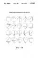
- FIG. 4illustrates the notation used for the vertical buses.
- Each vertical bushas 25 lines.
- Lines 1-4 and 15-17are long lines which run across the entire array.
- Lines 5-14consist of bidirectional general interconnect segments which are coupled through switching matrices and segment boxes as described below.
- Lines 18-25are uncommitted long lines which run the entire length of the array.
- FIG. 5illustrates the notation used for the horizontal buses.
- Each horizontal busis a 23 line bus in which lines 1-4 and 15 are long lines, lines 5-14 are bidirectional general interconnect segments, and lines 16-23 are uncommitted long lines.
- lines 1-4 and 15are long lines
- lines 5-14are bidirectional general interconnect segments
- lines 16-23are uncommitted long lines.
- the distinctions between the long lines, the bidirectional general interconnect (BGI) segments, and the uncommitted long linesare set out in detail below.
- the horizontal and vertical busesrequire means of interconnection. This occurs at the intersections of the horizontal buses and the vertical buses.
- the interconnections between the lines at the intersectionare made through programmable interconnect points, switch matrices, and segment boxes.
- FIG. 6illustrates the placement of the switch matrices in the interconnect structure.
- the switch matricesare positioned at the intersections of vertical bus 2-8 with horizontal buses 2-8.
- FIG. 6illustrates the placement of the switch matrices on horizontal bus 4 adjacent the configurable logic blocks R3C3, R3C4, R4C3, and R4C4. It can be seen that the switch matrices are positioned only on lines 5-14 of the bidirectional general interconnect BGI structure.
- the bidirectional general interconnect structureconsists of BGI segments which are two configurable logic blocks in length, spanning, in this case, from switch matrix 600, located on vertical bus 3, to switch matrix 601, located on vertical bus 5 in lines 5-9 of a bidirectional general interconnect.
- Switch matrix 602is coupled to BGI segments of line 10-14 which extend from vertical bus 2 to vertical bus 4 and vertical bus 4 to vertical bus 6. Vertical buses 2 and 6 are not shown in FIG. 6.
- connection to a BGI segmentallows propagation of the signal across a width equal to two configurable logic blocks on the array without passing through a switch matrix. This allows networks with fewer delays due to switch matrices.
- FIGS. 7 and 8illustrate the complete intersection between vertical buses 2-8 and horizontal buses 2-8, where a circle indicates a bidirectional programmable interconnect point controlled by a memory cell in the configuration memory.
- FIG. 7is the structure for the intersection of odd numbered vertical buses with odd numbered horizontal buses, and even numbered vertical buses with even numbered horizontal buses.
- FIG. 8is the structure for the even-odd and odd-even intersections between vertical and horizontal buses.
- horizontal long line 1is connectable to vertical long lines 1 and 4.
- Horizontal long line 2is connectable to vertical long lines 2 and 3.
- Horizontal long line 3is connectable to vertical long lines 2 and 3.
- Horizontal long line 4is connectable to vertical long lines 1 and 4.
- Horizontal long lines 1-4are connectable to vertical BGI segments 5-8, respectively. Also, vertical long lines 1-4 are connectable to horizontal BGI segments 5-8, respectively.
- Horizontal BGI segments 5-9are coupled to the left side 700 of a switch matrix.
- the right side 701 of the switch matrixprovides horizontal BGI segment 5 which is connectable to vertical BGI segment 14.
- the horizontal BGI segment 6 output from the right side 701 of the switch matrixis connectable to vertical BGI segment 13.
- Horizontal BGI segment 7 from the switch matrixis coupled through a programmable interconnection point (PIP) to vertical BGI segment 12.
- Horizontal BGI segment 8 from the switch matrix side 701is coupled through PIP to vertical BGI segment 11.
- Horizontal BGI segment 9 output from the right side 701 of the switch matrixis coupled through a PIP to vertical BGI segment 10.
- the BGI segments 10-14 of the horizontal busare connectable through PIPs to the BGI segments in the vertical bus 9-5 and 10-14 in the configuration shown.
- BGI segments 10-13 of the horizontal busare connectable to the even numbered uncommitted long lines 18, 20, 22, and 24 through PIPs as shown.
- the horizontal long line 15passes through the intersection without being connectable to any other line.
- the odd numbered uncommitted long lines 17, 19, 21, and 23 in the horizontal busare connectable through PIPs to the vertical BGI segments 10-13 as shown.
- FIG. 8The interconnection of the even or odd numbered vertical buses with odd or even numbered horizontal buses, respectively, is shown in FIG. 8. As with the intersection shown in FIG. 7, the horizontal lines in the intersection structure of FIG. 8 are connectable through PIPs and the switch matrix to the vertical lines.
- Horizontal long line 1is connectable to vertical long lines 1 and 4.
- Horizontal long line 2is connectable to vertical long lines 2 and 3.
- Horizontal long line 3is connectable to vertical long lines 2 and 3.
- Horizontal long line 4is connectable to vertical long lines 1 and 4.
- horizontal long lines 1-4are connectable to vertical BGI segments 13, 12, 11 and 10 respectively.
- Vertical long lines 1-4are connectable to horizontal BGI segments 10-13, respectively.
- Horizontal BGI segments 5-9are connectable to the BGI segments 5-14 as shown in the figure and to the even numbered uncommitted long lines 18, 20, 22, and 24.
- the horizontal BGI segments 10-14are connectable to the vertical BGI segments 9-5 and through the switching matrix to the adjacent BGI segments of lines 10-14 in both the vertical and the horizontal buses.
- the even numbered uncommitted long lines 16, 18, 20, and 22 on the horizontal busare connectable to the vertical BGI segments 6-9 as shown.
- FIG. 9illustrates the intersection of horizontal buses 1 and 9 with the even numbered vertical buses 2-8 and vertical buses 1 and 9.
- FIG. 10illustrates the intersection of the horizontal buses 1 and 9 with the odd numbered vertical buses 3-7.
- the horizontal long lines 1-4are connectable to vertical long lines 1-4 as shown.
- the horizontal BGI segments 5-9are connectable through the segment box to vertical BGI segments 5-9.
- the horizontal BGI segments 10-14are connectable to vertical BGI segments 10-14.
- the BGI segments 11-14are connectable to the odd numbered vertical uncommitted long lines 19, 21, 23, and 25.
- the odd numbered horizontal uncommitted long lines 17, 19, 21, and 23 on the horizontal busare connectable to the vertical BGI segments 10-13 as shown.
- horizontal long lines 1-4 on the horizontal busare connectable respectively to vertical long lines 1-4.
- the horizontal BGI segments 5-9are connectable to the vertical BGI segments 5-9 and to the even numbered vertical uncommitted long lines 18, 20, 22, and 24 as shown.
- the horizontal BGI segments 10-14are connected to the segment box as are the vertical BGI segments 10-14.
- the even numbered uncommitted long lines 16, 18, 20, and 22 on the horizontal busare connectable to vertical BGI segments 6-9 as shown.
- FIG. 11illustrates the intersection of horizontal bus 1 with vertical bus 1.
- the lines 1-14 in the horizontal busare connectable respectively to lines 1-14 in the vertical bus.
- the even numbered uncommitted long lines 18, 20, 22, and 24 on the vertical busare connectable to horizontal BGI segments 6-9.
- the odd numbered uncommitted long lines 17, 19, 21, and 23 on the horizontal busare connectable to the vertical BGI segments 6-9.
- FIG. 12illustrates the intersection of horizontal bus 1 with vertical bus 9.
- the horizontal long line 1is connectable to vertical long lines 1 and 4.
- Horizontal long line 2is connectable to vertical long lines 2 and 3.
- Horizontal long lines 3-4 and BGI segments 5-14are connectable respectively to vertical long lines 3-4 and BGI segments 5-14.
- the even numbered uncommitted long lines 18, 20, 22, and 24 on the vertical busare connectable to horizontal BGI segment 6-9.
- the odd numbered uncommitted long lines 17, 19, 21, and 23 on the horizontal busare connectable to the vertical BGI segments 6-9.
- FIG. 13illustrates the intersection of horizontal bus 9 with vertical bus 1.
- the horizontal long lines 1-4 and BGI segments 5-14are connectable to the vertical long lines 1-4 and BGI segments 5-14, respectively.
- horizontal line 3is connectable to vertical long lines 2 and 3
- horizontal long line 4is connectable to vertical long lines 1 and 4.
- the horizontal BGI segments 6-9are also connectable to the even numbered uncommitted long lines 18, 20, 22 and 24 on the vertical bus.
- the odd numbered uncommitted long lines 17, 19, 21, and 23 on the horizontal busare connectable to vertical BGI segments 6-9.
- FIG. 14illustrates the intersection of horizontal bus 9 with vertical bus 9.
- Horizontal long lines 1-4 and BGI segments 5-14are connectable to vertical long lines 1-4 and BGI segments 5-14, respectively.
- Horizontal BGI segments 6-9are also connectable to the even numbered uncommitted long lines 18, 20, 22 and 24 on the vertical bus.
- the odd numbered uncommitted long lines 17, 19, 21, and 23 on the horizontal busare connectable to vertical BGI segments 6-9.
- FIG. 14Ashows a corner connection that can be used at the intersections of horizontal bus 1 and vertical bus 1, horizontal bus 1 and vertical bus 9, horizontal bus 9 and vertical bus 9, and horizontal bus 9 and vertical bus 1. It has the advantage that it is a single layout that can be used at all four corners while accomplishing the ability to route signals from the long lines 1-4 completely around the perimeter of the chip.
- horizontal lines long 1-4 and BGI segments 5-14are connectable to vertical long lines 1-4 and 5-14, respectively.
- Horizontal long line 1is connectable to vertical long lines 1 and 4
- horizontal long line 2is connectable to vertical long lines 2 and 3
- horizontal long line 3is connectable to vertical long lines 2 and 3
- horizontal long line 4is connectable to vertical long lines 1 and 4.
- horizontal BGI segment 14is connectable to vertical BGI segment 5
- horizontal BGI segment 13is connectable to vertical BGI segment 6
- horizontal BGI segment 12is connectable to vertical BGI segment 7
- horizontal BGI segment 11is connectable to vertical BGI segment 8
- horizontal BGI segment 10is connectable to vertical BGI segment 9
- horizontal BGI segment 9is connectable to vertical BGI segment 10
- horizontal BGI segment 8is connectable to vertical BGI segment 11
- horizontal BGI segment 7is connectable to vertical BGI segment 12
- horizontal BGI segment 6is connectable to vertical 13
- horizontal BGI segment 5is connectable to vertical BGI segment 14.
- horizontal BGI segments 6-9are connectable to the even numbered, uncommitted long lines 18, 20, 22, and 24 on the vertical bus. The even numbered long lines 16, 18, 20, 22 on the horizontal bus are connectable to vertical BGI segments 6-9.
- FIG. 15illustrates the connection of the global clock and global reset signals on vertical lines 16 and 17.
- the global clock signalis supplied from an input buffer 1500 to line 1501.
- Line 1501is directly connected to line 16 in all vertical buses.
- the global reset signalis supplied at global reset buffer 1502.
- the output of the global reset bufferis supplied on line 1503 to line 17 on all the vertical buses.
- the lines 16 and 17 of the vertical busesare directly connected to the input/output blocks as schematically illustrated in FIG. 15 and to each of the configurable logic blocks.
- the direct connections to the configurable logic blocksare shown only to a few of the blocks in the upper left hand corner of the array for clarity of the figure.
- FIG. 15Ashows the connection of lines 16 and 17 of the vertical buses to the configurable logic blocks.
- lines 16 and 17are connected only to the input/output blocks as shown.
- FIG. 15Bshows the configurable path from an input/output pad to an IOB or to the global or alternate buffers. It can be seen that the pad 1510 is connected across line 1511 through buffer 1512 to line 1513. Line 1513 is passed through pass transistor 1514 to an IOB input path 1515 or through pass transistor 1516 to the buffer input circuitry on line 1517. A memory cell 1518 in the configuration store controls which pass transistor (1514 or 1516) is enabled.
- FIG. 15Cillustrates the input circuitry to the global clock buffer.
- Input 1 of IOB 2 and 9are connected to provide a signal on lines 1518 and 1519 as inputs to 8 to 1 multiplexer 1521.
- a clock input pin at IOB 110is connected to line 1520 as illustrated in FIG. 15B as input to multiplexer 1521.
- Lines 14 and 15 in vertical bus 1 and lines 14 and 15 in horizontal bus 1are also coupled as inputs to configurable multiplexer 1521.
- the direct connect output X4 on the configurable logic block in row 1, column 1is directly connected as well as a input to the multiplexer 1521.
- the direct link from an adjacent CLB to the multiplexer 1521 across line 1524provides added flexibility for the generation of the global clock on chip.
- the configuration storecontrols the multiplexer 1521 to supply a clock signal on line 1522 to the global clock buffer 1523.
- FIG. 16illustrates the connection of line 15 in the vertical and horizontal buses. It is designed to perform the function of a local clock for an input/output block or a configurable logic block or as a clock enable signal.
- the line 15 in horizontal busesis connectable to a variety of sources including outputs from configurable logic blocks and the alternate buffers.
- the line 15 in the horizontal busesare connectable to the horizontal alternate buffer 1600 which generates the signal on line 1601.
- a bidirectional buffersuch as buffer 1602.
- Each bidirectional bufferincludes a configurable tristate buffer connected from line 1601 to line 15 in the respective horizontal bus.
- a configurable tristate buffer connected from line 15 on the respective horizontal bussupplies an output to line 1601.
- the configurable tristate buffersare each controlled by a memory cell in the configuration memory.
- the vertical alternate buffer 1603generates a signal on line 1604.
- Line 15 on each vertical busis connected to a bidirectional buffer, e.g. buffer 1605.
- Each vertical -- bidirectional bufferhas a first tristate buffer connected from line 1604 to line 15 in the respective vertical bus and a tristate buffer connected from line 15 in the respective vertical bus to line 1605.
- Each of the tristate buffersis controllable from a storage cell in the configuration memory.
- the line 15's in vertical buses 1 and 9are connected respectively to the input/output blocks on the left side and right side of the chip.
- the line 15's in horizontal buses 1 and 9are connected to the input/output blocks on the top and bottom of the chip as shown.
- FIG. 16Ashows the connection of the input/output blocks to line 15 and the connection of the configurable logic blocks to line 15.
- Each complex IOB 1606has a K input directly connected to line 15 on its adjacent vertical or horizontal bus.
- Each simple IOB 1607is capable of supplying an input signal to line 15 of a horizontal and vertical bus through a PIP.
- Each configurable logic block as shown in FIG. 16Ahas inputs labeled K1, K2, K3 and K4.
- the input K1is connected to line 15 in the horizontal bus above the block.
- Input K2is directly connected to line 15 in the vertical bus to the right of the block.
- Input K3is directly connected to line 15 in the horizontal bus below the block.
- Input K4is directly connected to the vertical bus to the left of the block.
- each configurable logic blockhas output Y1, Y2, Y3 and Y4.
- the output Y1is connectable through a PIP to line 15 in the horizontal bus above the block.
- Output Y2is connectable through a PIP to line 15 in the vertical bus to the right of the block.
- Output Y3is connectable through a PIP to line 15 in the horizontal bus below the block.
- Output Y4is connectable through a PIP to line 15 in the vertical bus to the left of the block.
- the line 1604 connected to the vertical alternate buffer and the line 1601 connected to the horizontal alternate buffercan receive inputs from a number of sources including device pins, and interconnects via PIPs.
- the signal on line 1601can be supplied to all configurable logic blocks and input/output blocks adjacent the horizontal buses with the exception of input/output blocks on the left side and right side of the chip.
- the signal on line 1604can be globally supplied across the chip, with the exception that it cannot be directly connected to the input/output blocks on the top and bottom of the chip.
- a signalcan be generated in configurable logic block R1C1, supplied to line 15 of vertical bus 2 through the bidirectional buffer 1608 to line 1604. From line 1604, it can be supplied anywhere in the chip. A similar net can be formed along horizontal buses.
- This line 15 structureallows the registers in any configurable logic block to receive a clock from one of five sources.
- the sourcesinclude the global clock GK supplied on vertical bus line 16, and the local clocks K1, K2, K3, and K4 which are connected to line 15 on four adjacent interconnect buses.
- the registers in a complex input/output blockcan receive a clock from two sources.
- the first sourceis line 16 in the adjacent vertical bus at its GK input and from an input K on the configurable I/0 block connectable through a PIP to line 15 on either a horizontal or vertical bus depending on the location of the input/output block
- Each line 15 in either a horizontal or a vertical buscan carry a signal obtained from one of four sources.
- the four sourcesinclude an alternate buffer, an adjacent configurable logic block, an adjacent input/output block, and a configurable logic block which has supplied a signal to line 15 of a different bus which has in turn been connected through the bidirectional buffers to levels 1601 or 1604.
- the long lines connecting to that buffercan either be independent where the bidirectional buffers are configured to supply a high impedance state to the long line, or they can use the alternate buffer as a source.
- FIG. 16Billustrates the input structure to the vertical alternate buffer 1603.
- the input to the vertical alternate buffer 1603is provided on line 1610 at the output of the configurable multiplexer 1611.
- the signal on line 1610is connected for supply as output signals at IOB 1612 and at IOB 1613.
- Inputs to the multiplexer 1611include an oscillator signal OSC as generated by the circuitry illustrated in FIGS. 16D and 16E.
- an input signal from IOB 1612is an alternative input to multiplexer 1611 across line 1614.
- a vertical clock input signalis supplied on line 1615 as input to multiplexer 1611 from IOB 1616 configured as shown in FIG. 15B.
- Long lines 4 and 15 of the vertical bus 9 and long lines 4 and 15 of the horizontal bus 9are also connected as inputs to multiplexer 1611.
- the final input to multiplexer 1611is a direct link from output X2 of the configurable logic block in row 8, column 8, across line 1617.
- the vertical alternate buffer 1603also includes a memory cell 1618 for tristate control.
- FIG. 16Cillustrates the input structure for the horizontal alternate buffer 1600.
- the horizontal alternate bufferis tristatable in response to the signal at memory cell 1620.
- the input to horizontal alternate buffer 1600is supplied on line 1621 at the output of the configurable multiplexer 1622.
- Inputs to the configurable multiplexer 1622include the horizontal clock input signal on line 1623, and input signals on lines 1624 and 1625 from input/output structures 1626 and 1627, respectively.
- the vertical bus long lines 4 and 15 and horizontal bus long lines 4 and 15are connectable as inputs as well to the multiplexer 1622.
- a direct link from the configurable logic block in row 8, column 1, output X4is coupled across line 1628 as an input to multiplexer 1622.
- the on chip oscillator which supplies the OSC signal as one input to the multiplexer 1611 driving the vertical alternate buffer 1603is shown in FIG. 16D.
- the OSC signalis provided at the output of multiplexer 1630 which is controlled by memory cell 1631.
- Inputs to multiplexer 1630include the signal on line 1632 which is supplied at the output of inverting buffer 1633.
- the input to inverting buffer 1633is the signal on line 1634 which is supplied at the output of the oscillator amplifier 1635.
- the input to the oscillator amplifier 1635is supplied at IOB 1636.
- IOB 1637is coupled directly to line 1634.
- Line 1634is supplied through inverting buffer 1638 as a clock input on line 1639 to register 1640.
- Register 1640is connected as a divide-by-two circuit by coupling line coupled from its Q output through inverting buffer 1642 as the D input to register 1640.
- the Q output of register 1640is supplied on line 1643 as a second input to multiplexer 1630.
- Pad 1637is coupled to line 1650 and pad 1636 is coupled to line 1651.
- Resistor R1is connected between line 1650 and 1651.
- Line 1651is coupled through capacitor C1 to GROUND and through crystal 1652 to line 1653.
- Line 1653is coupled through capacitor C2 to GROUND and through resistor R2 to line 1650.
- the divide-by-two option in the oscillator circuitis provided to ensure symmetry of the signal.
- the output of the 2:1 multiplexer 1630gives this choice, and is set during device configuration.
- the paths 1637 and 1636are configurable as shown in FIG. 15B to behave as standard IOBs.
- the oscillator circuitbecomes active before configuration is complete to allow it to stabilize.
- FIG. 17The structure of the programmable interconnect points (PIPs) is shown in FIG. 17 and an alternative structure is shown in FIG. 18.
- the structure in FIG. 17illustrates that for an intersecting conductive segment, such as long lines 1700 and 1701, with long line 1702, a PIP is implemented using a pass transistor.
- pass transistor 1703provides for interconnection between lines 1702 and 1701.
- Pass transistor 1704provides for interconnection between lines 1700 and 1702.
- the memory cell 1705 from the configuration storecontrols the pass transistor 1703 to provide a bidirectional path between the lines.
- memory cell 1706controls pass transistor 1704 to provide the bidirectional path.
- FIG. 17illustrates that a PIP can be implemented as a multi-source multiplexer 1800.
- Multiplexer 1800can have three sources, source 1, source 2, and source 3, and select a destination line 1801 in response to memory cells 1802 in the configuration store.
- two memory cellscan provide for selection from among three or four sources.
- the equivalent symbol for the circuit using multiplexer 1800is shown at 1803. It should be recognized that the multiplexer implementation is a unidirectional interconnect which allows for connection from any one of the source lines to the destination line and not vice versa. Furthermore, only one source line can be activated for a given operation.
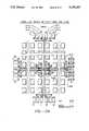
- FIG. 19illustrates the implementation of the switch matrix according to the present invention.
- Each switch matrixhas five connections on the top labeled 1-5, five connections on the right side labeled 6-10, five connections on the bottom labeled 11-15, and five connections on the left side labeled 16-20.
- Line 1is connectable through PIP 1-20 to line 20, through PIP 1-6 to line 6, through PIP 1-11 to line 11, and through PIP 1-15 to line 15.
- Line 2is connectable through PIP 2-19 to line 19, PIP 2-7 to line 7, PIP 21-4 to line 14, and PIP 2-15 to line 15.
- Line 3is connectable through PIP 3-18 to line 18, PIP 3-8 to line 8, PIP 3-13 to line 13, and PIP 1-14 to line 14.
- Line 4is connectable through PIP 4-17 to line 17, PIP 4-9 to line 9, PIP 4-12 to line 12, and PIP 4-13 to line 13.
- Line 5is connectable through 5-16 to line 16, PIP 5-10 to line 10, PIP 5-11 to line 11, and PIP 5-12 to line 12.
- connections of lines 6-10include the following.
- Line 6is connectable through PIP 6-15 to line 15, PIP 6-16 to line 16, and through PIP 6-20 to line 20.
- Line 7is connectable through PIP 7-14 to line 14, and through PIP 7-19 to line 19, and PIP 7-20 to line 20.
- Line 8is connectable through PIP 8-13 to line 13, PIP 8-18 to line 18, and PIP 8-19 to line 19.
- Line 9is connectable through PIP 9-12 to line 12, PIP 9-17 to line 17, and PIP 9-18 to line 18.
- Line 10is connectable through PIP 10-11 to line 11, PIP 10-16 to line 16, and PIP 10-17 to line 17.
- connection of line 20 through PIP 20-15 to line 15the connection of line 19 through PIP 19-14 to line 14, the connection of line 18 through PIP 18-13 to line 13, the connection of line 17 through PIP 17-12 to line 12, and the connection of line 16 through PlP 16-11 to line 11.
- FIG. 20illustrates the repowering buffer which is used with a horizontal segment and a vertical segment for each switching matrix.
- Repowering buffersare used for reshaping a signal after it has passed through a number of PIPs.
- Each repowering bufferadds delay to the net being routed. Thus, for short nets, the designer would want to avoid using the repowering buffers.
- the repowering buffer as shown in FIG. 20is connected on one of the bidirectional general interconnect segments designated line X in the figure, where X is one of lines 5-14 in a horizontal or vertical bus.
- Line Xenters the left side of the repowering buffer at point 2000.
- Point 2000is supplied as input to a first tristate buffer 2001.
- the output of the tristate buffer 2001is connected to point 2002 which is supplied at the output of the repowering buffer back to line X.
- Point 2002is also supplied at the input of a tristate buffer 2003.
- the output of the tristate buffer 2003is connected at point 2000 for supply of the signal in the right to left direction.
- a third path, through pass transistor 2004,is supplied between points 2000 and 2002.
- the first memory cell M1 and a second memory cell M2control the operation of the repowering buffer.
- the true output of memory cell M1is supplied to AND-gate 2005.
- the complement output of memory cell M2is supplied as a second input to AND-gate 2005.
- the output of AND-gate 2005is the tristate enable input to buffer 2003.
- the inverted output of memory cell M1is supplied at a first input to AND-gate 2006.
- the second input to AND-gate 2006is the inverted output of memory cell 2002.
- the output of AND-gate 2006is the tristate control signal for buffer 2001.
- the true output of memory cell M2is supplied to control the pass transistor 2004.
- the repowering buffer shown in FIG. 20supplies for repowering of a signal propagating in either direction along line X.
- the pass transistor 2004allows for bypassing of the repowering buffer.
- the line location of the repowering buffer for a given switching matrix or segment boxshould be determined as meets the needs of a particular application.
- the repowering buffershould be utilized for current CMOS technology for any network path passing through around four or more PIPs, and not going through a CLB or IOB.
- FIG. 21illustrates the interconnection options for a switch matrix using the PIP array as shown in FIG. 19.
- the figureis a graphical representation showing the possible interconnections of each of the connections 1-20 through the switching matrix.
- the possible interconnections of connection 1is shown in the upper left hand corner.
- the possible interconnections of connection 20are shown in the lower right hand corner.
- FIG. 22illustrates the interconnection array for the segment box on vertical buses 1 and 9. It can be seen that the segment box is an alternative switch matrix design, adapted for the peripheral buses.
- Each segment boxhas 20 input connections, five on each side, as illustrated in the figure.
- the input connections 20 and 6are directly connected, input connections 19 and 7 are connected, inputs 18 and 8 are connected, inputs 17 and 9 are connected, and inputs 16 and 10 are connected.
- Inputs 1 and 15are connectable through PIPs to the line connecting inputs 20 and 6.
- Inputs 2 and 14are connectable through respective PIPs to the line connecting inputs 9 and 7.
- Inputs 3 and 13are connectable through PIPs to the line connecting inputs 18 and 8.
- Inputs 4 and 12are connectable through PIPs to the line connecting inputs 17 and 9.
- inputs 5 and 11are connectable through PIPs to the line connecting inputs 16 and 10.
- the segment box on the horizontal buses 1 and 9is shown in FIG. 23.
- inputs 1 and 15are connected directly
- inputs 2 and 14are connected directly
- inputs 3 and 13are connected directly
- inputs 4 and 12are connected directly
- inputs 5 and 11are connected directly.
- Inputs 20 and 6are connectable through PIPs to the line connecting inputs 1 and 15
- inputs 19 and 7are connectable through PIPs to the line connecting inputs 2 and 14.
- Inputs 18 and 8are connectable through PIPs to the line connecting inputs 3 and 13.
- Inputs 17 and 9are connectable through PIPs to the line connecting inputs 4 and 12.
- inputs 16 and 10are connectable through PIPs to the line connecting inputs 5 and 11.
- FIG. 24graphically illustrates in the style of FIG. 21, the possible interconnections for each input to a segment box. These possible interconnections apply equally to the segment boxes on the vertical buses and to the segment boxes on the horizontal buses.
- FIG. 25An overview block diagram of a configurable logic block is set out in FIG. 25.
- the configurable logic block 2500 shown in FIG. 25consists of a combinational function and control generator 2501 which receives inputs from four sides, schematically illustrated by buses 2502-1, 2502-2, 2502-3, and 2502-4.
- the combinational function and control generator 2501communicates with four independently configurable output ports 2503-1, 2503-2, 2503-3, and 2503-4.
- the output portsreceive signals and supply feedback signals to and from the combinational function and control generator 2501 across respective buses 2504-1, 2504-2, 2504-3, and 2504-4.
- Each output portsupplies a plurality of output signals, schematically illustrated by the respective output buses 2505-1, 2505-2, 2505-3, and 2505-4.
- FIG. 25illustrates at a high level the symmetry of the configurable logic block 2500.
- Input signalscan be received from all four sides of the block, likewise, output signals can be supplied to any of the four sides of the block.
- input signals from the input bus 2502can be used to generate output signals across bus 2505-1, 2505-2, 2505-3, or 2505-4. Similar flexibility is provided from all of the other input buses in the configurable logic block.
- the inputs and outputs to the configurable logic blockare set out in FIG. 26. Also, a notation for the inputs and outputs is provided. It can be seen that input signals along the top side of the block are labeled A1 through D1, EM1, EN1, FM1, FN1, G1, H1, and K1. The outputs are labelled X1 and Y1. Similarly, the suffix 2 is applied to the right side of the block, the suffix 3 is applied to the bottom of the block, and the suffix 4 is applied to the left side of the block. On the left side of the block, additional inputs GR and GK for global reset and global clock signals are provided.
- the inputs A1 through A4 and B1 through B4are long line inputs.
- Inputs C1 through C4 and D1 through D4are inputs coupled to the bidirectional general interconnect segments for logic signals.
- the inputs EM1 through EM4, FM1 through FM4, EN1 through EN4, and FN1 through FN4are direct connect inputs.
- the inputs G1 through G4 and H1 through H4are inputs to the bidirectional general interconnect segments for control signals.
- the inputs K1 through K4are long line inputs from bus line 15 used for clock and clock enable functions.
- Outputsare supplied at terminals X1 through X4 and Y1 through Y4.
- Direct connect structuresare connected to X1 through X4.
- the general interconnect structuresare coupled to outputs Y1 through Y4.
- Each input/output blockis coupled to memory cells in the configuration memory, the states of which control the configuration of the IOB.
- an IOBallows data to pass in two directions: (i) from an input/output pad to the programmable general connect and specific CLBs; (ii) from the programmable general connect and specific CLBs to a pad.
- the configuration of an IOBsets the type of conditioning the signal receives on passing through the IOB.
- the padmay or may not be bonded to a physical package pin.
- FIGS. 27 and 28illustrate the inputs and outputs of the complex and simple IOBs, respectively. These figures can be referred to when reviewing the interconnect structures described in the following sections.
- the signal DIcorresponds to a direct connect input signal.
- the signal Icorresponds to an input connection to the configurable interconnect.
- the signal Ocorresponds a plurality of outgoing signals from the configurable interconnect or direct connects.
- the other labeled signalsare control signals.
- the signal DIis a direct connect input signal.
- the signal Iis an input connection to the configurable interconnect.
- the signal Ocorresponds to outgoing signals from the configurable interconnect or direct connects.
- the IEN and OEN signalsare input control signals.
- the configurable interconnect structureprovides a means of connecting the CLBs and IOBs together. It is divided into two major categories, called the direct connect and the programmable general connect.
- the programmable general connectincludes long lines, the bidirectional general interconnects and the uncommitted long lines.
- netsThe programmed connections required between the blocks for a user application are referred to as nets.
- a netcan have single or multiple sources, and single or multiple destinations.
- the type of interconnect resource used to construct a netis determined from availability to the software routing algorithm and the propagation delay allowed for the net. The allowed propagation delay is defined by user application.
- FIGS. 29-34The direct connect structure is illustrated chiefly in FIGS. 29-34.
- FIGS. 29 and 30in combination show all the direct connections supplied as inputs EM1 through EM4, EN1 through EN4, FM1 through FM4, and FN1 through FN4 supplied from the outputs X1 through X4 of eight neighbor CLBs.
- FIG. 29the connection of next adjacent CLBs to the inputs FM1 through FM4 and FN1 through FN4 are shown.
- the connection X4 from CLB of row i-2 column jis coupled to the input FN1 of the CLB of row i in column j.
- Output X2 of CLB of row i-2 in column jis coupled to the input FM3.
- Output X1 of CLB of row i and column j+2is coupled to the input FN2.
- Output X3 of CLB of row i column j+2is coupled to the input FM4.
- the output X4 of CLB of row i+2 in column jis coupled to the input FM1 of the center CLB.
- the output X2 of row i+2 and column jis coupled to the input FN3 of the center CLB.
- the output X3 of the CLB of row i and column j-2is coupled to the input FN4.
- Output X1 of the CLB of row i in column j-2is coupled to the input FM2.
- the output X4 of the CLB in row i-1 and column jis coupled to the input EN1 of the center CLB in row i and column j.
- Output X2 of the CLB in row i-1 and column jis coupled to the input EM3 in the center CLB.
- Output X1 of the CLB in row i and column j+1is coupled to the input EN2 of the center CLB.
- the output X3 of the CLB in row i column j+1is coupled to the input EM4.
- the output X2 of the CLB in row i+1 and column jis coupled to the input EN3.
- the output X4 of the CLB in row i+1 in column jis coupled to the input EM1.
- the output X3 of the CLB in row i and column j-1is coupled to the input EN4.
- the output X1 in the CLB in row i, column j-1is coupled to the input EM2.
- FIGS. 29 and 30illustrate that the CLBs in the center of the array are directly coupled to eight neighbor CLBs. Further, the interconnections allow for direction of data flow in any direction through the direct connect structure among CLBs.
- the CLB at row i-1, column j+1; row i+1, column j+1; row i-1, column j-1; and row i+1 column j-1could be connected in place the four outer CLBs shown in FIGS. 29 and 30. This would provide eight neighbors with diagonal interconnection paths through the device. However, it is found that the ability to traverse a row or column with a direct connect structure provides for enhanced speed in transferring signals across the device.
- FIG. 31illustrates the connection of the outputs X1 through X4 on the center CLB in row i column j to the eight neighbor CLBs.
- the output X4 of the CLB in the centeris connected to the input FM1 of the CLB in row i-2, column j; the input EM1 of the CLB in row i-1 column j; the input EN1 of the CLB in row i+1, column j; and the input FN1 in the CLB of row i+2, column j.
- the output X1is coupled to the input FN2 of the CLB in row i, column j-2; the input EN2 in the CLB in row i, column j-1; the input EM2 in the CLB in row i, column j+1; and the input FM2 in the CLB in row i, column j+2.
- the output X2is coupled to the inputs FN3 and EN3 in the CLBs in rows i-2 and i-1, column j, respectively, and to the inputs EM3 and FM3 in the CLBs of rows i+1 and i+2, of column j, respectively.
- the output X3is coupled to the inputs FM4 and EM4 of the CLBs in row i columns j-2 and j-1, respectively, and to the inputs EN4 and FN4 in the CLBs of row i columns j+1 and j+2, respectively.
- FIGS. 32-34The direct connections on the peripheral CLBs which include direct connections to the IOBs are shown in FIGS. 32-34.
- the figuresare shown with the IOBs along the left side of the figure so that the columns of peripheral CLBs shown are columns 1 and 2.
- the connectionsapply as well for structures in which the peripheral CLBs are on rows 1 and 2 rather than columns 1 and 2, columns 7 and 8 rather than columns 1 and 2, and rows 7 and 8 rather than columns 1 and 2.
- the connectionsare just rotated where appropriate.
- FIG. 32shows the connection of the CLB in column 1 row i, for i between 3 and 6. Also, the connections of the CLB in column 2 row i are shown.
- the IOBs in the configurable gate array of the present inventionare grouped into three blocks per row or column of the array.
- Ri1, Ri2, and Ri3there are three IOBs Ri1, Ri2, and Ri3.
- Ri1 and Ri3are complex IOBs while Ri2 is a simple IOB.
- Eachhas a multiplexer receiving a plurality of signals for supply as the output signal to the associated pin. These inputs are shown by the reference O.
- the output X1 in the CLB C1Riis coupled directly to the output in the IOB Ri1, to the input EM2 in the CLB C2Ri and to the input FM2 in the CLB C3Ri.
- the output X2 of the CLB C1Riis coupled directly to the inputs FN3 and EN3 of the CLBs in column 1 rows Ri-2 and i-1, respectively. Also, the output X2 is coupled directly to the inputs EM3 and FM3 in the CLBs in column 1 rows Ri+1 and Ri+2, respectively.
- the output X3 of the CLB C1Riis coupled directly to the terminal O in the complex IOB Ri3 and to the EN4 and FN4 inputs of the CLBs C2Ri and C3Ri, respectively.
- the output X4 of the CLB C1Riis coupled directly to the O terminal of the simple IOB Ri2 and directly to the FM1 and EM1 terminals of CLBs C1Ri-2 and C1Ri-1, respectively. Also, the output X4 of the CLB C1Ri is coupled directly to the EN1 and FN1 inputs of CLB in column 1 rows i+1 and i+2, respectively.
- the output X1 in the CLB C2Riis coupled directly to the O terminal of the complex IOB Ri1, and to the EN2 terminal of the CLB C1Ri. Output X1 is also coupled to the EM2 and FM2 inputs of CLBs C3Ri and C4Ri, respectively.
- the output X2 of the CLB C2Riis coupled directly to the inputs FN3 and EN3 of the CLBs C2Ri-2 and C2Ri-1.
- the output X2 of C2Riis also coupled to the EM3 and FM3 inputs of CLBs C2Ri+1 and C2Ri+2.
- the output X3 of the CLB C2Riis coupled directly to the O terminal of the complex IOB Ri3, to the EM4 input of the CLB C1Ri to the EN4 input of CLB C3Ri and to the input FN4 of CLB C4Ri.
- the output terminal X4 of the CLB C2Riis connected directly to the inputs FM1 and EM1 of CLBs C2Ri-2 and C2Ri-1. Output X4 is also coupled to the inputs EN1 and FN1 of CLBs C2Ri+1 and C2Ri+2, respectively. In addition, the output X4 of CLB C2Ri is connected directly to the O terminal of the simple IOB Ri2.
- the inputs EM1 through EM4 and EN1 through EN4 of the CLB C1Riare shown in FIG. 33.
- the terminal EM1is coupled to receive the output X4 of CLB C1Ri+1.
- the input EN1is coupled to receive the output X4 of the CLB C1Ri-1.
- the input EM2is coupled to receive an input from the complex IOB Ri3.
- the input EN2is coupled to receive the output X1 of the CLB C2Ri.
- the input EM3is coupled to receive the output X2 of the CLB C1Ri-1.
- the input EN3is coupled to receive the output X2 of the CLB C1Ri+1.
- the input EM4is coupled to receive the output X3 of the CLB C2Ri.
- the input EN4is coupled to receive an input from the complex IOB Ri1.
- the outputs X4 of CLBs C1Ri-2 and C2Ri-2are connected respectively to the FN1 inputs of CLBs C1Ri and C2Ri.
- the outputs X2 of the CLBs C1Ri-2 and C2Ri-2are connected directly to the inputs FM3 of CLBs C1Ri and C2Ri.
- the outputs X1 of the CLBs C3Ri and C4Riare connected directly to the FN2 inputs of CLBs C1Ri and C2Ri, respectively.
- the outputs X3 of the CLBs C3Ri and C4Riare connected directly to the FM4 inputs of C1Ri and C2Ri.
- the outputs X2 of the CLBs C1Ri+2 and C2Ri+2are connected directly to the FN3 inputs of CLBs C1Ri and C2Ri, respectively.
- the outputs X4 of the CLBs C1Ri+2 and C2Ri+2are connected directly to the FM1 inputs of CLBs C1Ri and C2Ri, respectively.
- the terminal DI of the complex IOB Ri1is coupled directly to the FN4 input of CLB C2Ri.
- the input DI received from the simple IOB Ri2is coupled directly to the FN4 input and FM2 input of the CLB C1Ri.
- the input signal DI derived from the complex IOB Ri3is coupled directly to the FM2 input of CLB C2Ri.
- the programmable general connectis illustrated in FIGS. 35-49. It provides a means for routing nets around the device.
- the CLBs and IOBsare linked through this network by means of programmable interconnection points PIPs.
- the programmable general connectis subdivided into the long lines and the BGI segments, which are lines incorporating metal segments spanning one or two CLBs, usually terminating in a switching matrix or segment box as described above with reference to FIGS. 4-24.
- FIG. 35shows the programmable connections of the outputs Y1 through Y4 to the long lines and BGI.
- the outputs Y1 through Y4are also connected to the uncommitted long lines as shown in FIG. 37. Also, the outputs are coupled differently to the vertical bus 1 and horizontal bus 1, vertical bus 9 and horizontal bus 9 as shown in FIG. 38 as it relates to the long lines 1-4 in the respective buses.
- FIG. 35shows that the output Y1 is coupled to PIPs associated with long lines 3, 4, and 15, and BGI segments 5, 9, 13, and 14 in HBUS i.
- the output Y2 of CLB CiRiis coupled to VBUS i+1 long lines 1 and 2 and 15, and BGI segments 5, 7, 11, and 14.
- Output Y3 of CiRiis coupled to HBUS i+1 long lines 1, 2, and 15, and to BGI segments 5, 8, 12, and 14.
- the output Y4 of CiRiis coupled to VBUS i long lines 3, 4, and 15, and to BGI segments 5, 6, 10, and 14.
- FIG. 35Also shown in FIG. 35 are the inputs to C1 through C4 and D1 through D4. These inputs are coupled as the unidirectional PIPs using four to one multiplexers in the preferred system to save on memory. One could use bidirectional PIPs, if desired.
- the input C1is coupled to BGI segments 7, 9, 11, and 13 on HBUS i.
- Input D1is coupled to BGI segments 6, 8, 10, and 12 on HBUS i.
- Input C2is coupled to VBUS i+1 BGI segments 6, 8, 10, and 12, while input D2 is coupled to VBUS i+1 BGI segments 7, 9, 11, and 13.
- the input C3is coupled to HBUS i+1 BGI segments 6, 8, 10, and 12.
- Input D3is coupled to HBUS i+1 BGI segments 7, 9, 11, and 13.
- the input C4is coupled to VBUS i BGI segments 7, 9, 11, and 13.
- the input D4is coupled to VBUS i BGI segments 6, 8, 10, and 12.
- FIG. 36shows the fixed inputs from the long lines and BGI segments to CLB CiRi from the adjacent buses.
- long line 4is coupled to input A1
- long line 3is coupled to input B1
- BGI segment 5is coupled to input G1
- BGI segment 14is coupled to input H1
- long line 15is coupled to input K1.
- long line 1is coupled to input A2
- long line 2is coupled to input B2
- BGI segment 5is coupled to input G2
- BGI segment 14is coupled to input H2
- long line 15is coupled to input K2.
- long line 1is coupled to input A3
- long line 2is coupled to input B3
- BGI segment 5is coupled to input G3
- BGI segment 14is coupled to input H3
- long line 15is coupled to input K3.
- long line 4is coupled to input A4, long line 3 is coupled to input B4, BGI segment 5 is coupled to input G4, BGI segment 14 is coupled to input H4, long line 15 is coupled to input K4, long line 16 is coupled to input GK, and long line 17 is coupled to input GR.
- FIG. 37The connection of the configurable logic blocks to the uncommitted long lines is shown in FIG. 37.
- Each CLBsuch as CLB R3C4
- CLB R3C4has outputs Y1 through Y4 coupled to one uncommitted long line each.
- the connectionswill not be recited because they are shown in FIG. 37.
- FIG. 37only lines 18-25 of the vertical buses, and lines 16-23 of the horizontal buses are shown, because these are the only uncommitted long lines.
- the CLB R3C4 output Y1is coupled to uncommitted long line 21 of HBUS 3.
- the output Y2 of R3C4is coupled to uncommitted long line 23 of VBUS 5.
- the output Y3is coupled to uncommitted long line 21 of HBUS 4.
- the output Y4is coupled to uncommitted long line 23 of VBUS 4. Note that the uncommitted long lines do not have programmable connections to inputs of CLBs. The selection of the connections of the outputs of the uncommitted long lines has been carried out to achieve a distributed uniform pattern that facilitates programming of nets through the array.
- FIG. 38shows the connection of the long lines 1-4 in HBUS 1, VBUS 1, VBUS 9, and HBUS 9.
- the figureshows utilization of the corner intersections of VBUS 9 with HBUS 1 and HBUS 9, and VBUS 1 with HBUS 1 and HBUS 9 to allow propagation of a signal supplied to any one of the four outer long lines all the way around the chip. This facilitates utilization of a single signal as a control input to all IOBs as desired.
- the outputs Y1 of CLBs in row 1are all connected to HBUS 1 long lines 1, 3, and 4 with the exception of the Y1 output of R1C8 which is coupled to HBUS 1 long lines 2, 3, and 4.
- the outputs Y2 of CLBs in row 1are all connected to HBUS 1 long line 2, with the exception of R1C8.
- the Y4 output of R1C8is coupled to HBUS 1 long line 1.
- the Y2 output of all CLBs in column 8, except for R8C8,is coupled to VBUS9 long lines 1, 2, and 4.
- the Y3 output of all CLBs in column 8, with the exception of C8R8,is coupled to VBUS 9 long line 3.
- the Y1 output of C8R8is coupled to VBUS 9 long line 4.
- the Y2 output of CLB C8R8is coupled to VBUS 9 long lines 1, 2, and 3.
- the Y3 outputs of all CLBs in row 8, with the exception of C1R8,are coupled to HBUS 9 long lines 1, 2, and 4.
- the Y4 output of CLBs in row 8, with the exception of C1R8,is coupled to HBUS 9 long line 3.
- the Y2 output of C1R8is coupled to long line 4 of HBUS 9.
- the Y3 output of C1R8is coupled to long lines 1, 2, and 3 of HBUS 9.
- the CLBs in column 1, with the exception of C1R1,are connected so that Y4 is connected to VBUS 1 long lines 1, 3, and 4, and Y1 is connected to VBUS 1 long line 2.
- the CLB C1R1 output Y4is connected to VBUS 1 long lines 2-4 and the output Y3 is connected to VBUS 1 long line 1.
- Passage of a signal on any long line about the periphery of the chipis enabled by the interconnect structure 5900 at the intersection of VBUS 9 and HBUS 1, and the interconnect structure 5901 at the intersection of VBUS 1 and HBUS 9.
- These structures 5900 and 5901allow connection of a signal on any one of the four long lines around the periphery to one of the two outer long lines on the respective buses, and vice versa.
- FIG. 39illustrates the long line reach between IOBs and CLBs.
- a signal input from an IOBcan be supplied directly as an input to a CLB with only one PIP delay.
- a signal output from a CLBcan be supplied as an output signal to an IOB with only one PlP delay.
- the signal Y1 generated at CLB R6C5can be supplied along long line 4 of HBUS 6 through PIP 6000 as an input across line 6001 to the simple IOB R6-2.
- a signal generated at CLB in the interior of the arraycan be quickly propagated to the outside of the chip.
- the symbol 6003 on long line 4 for the PIPcorresponds to an input to the multiplexer 4501 of FIG. 45.
- an input signal from the IOB R6-2 and IOB R6-1can be coupled through PIPs to long line 3 which is supplied as a direct input B1 to R6C5 and to R6C4.
- long line 3which is supplied as a direct input B1 to R6C5 and to R6C4.
- an input signal from R6-1can be supplied directly to a CLB in the interior of the device.
- Similar pathscan be seen from the IOBs C4-1, C4-2, C4-3, C5-1, C5-2, and C5-3 at the top or bottom of the chip. These connections are similarly made for IOBs at the end of each column or row in the chip.
- the four long lines 1-4 of each bushave a programmable pull up resistor at their ends (not shown). These four long lines are envisioned to be used for connectivity between the IOBs and CLBs in the center of the device, or long reach between CLBs.
- the pull up resistorcan be enabled by the program data in the configuration memory such that if no signal arrives at the line, the line can be taken to a logical one state. This stops lines from carrying spurious signals across the whole device.
- a second feature of the pull upis the ability to construct a wired-AND b driving the line from a number of CLBs or IOBs output buffers that are tristatable.
- Each output buffermay be configured such that when passing a logic zero, the buffer asserts a low to the long line. When passing a logic 1, the buffer asserts a tristate (high impedance) to the line. If no other buffer is driving the line (i.e., all buffers connected are in tristate--the logic 1 case for each) then the pull-up resistor forces a logic high onto the line, giving the result of the AND function required.
- FIGS. 40-49show connections to the IOB structure with the interconnect.
- FIG. 40the connections of the input terminals I and the output terminals O of the eight groups of input/output blocks along the top side of the array to horizontal bus 1 are shown.
- the circular symbols at the intersection of linesrefer to bidirectional PIP connections.
- the squares at the intersectionindicate a connection to the multiplexer in the IOB which generates the outgoing O signal.
- each IOB input terminal Iis coupled to one BGI segment and one uncommitted long line through a PIP.
- Each output terminal O in the IOBsis coupled to one uncommitted long line and one BGI segment at the input multiplexer.
- the input terminal I of the simple IOBs in respective centers of the tripletsare all coupled to long line 15 through a PIP.
- the distribution of the connectionshas been chosen to provide for a predictable scheme that facilitates programming of networks on the device.
- a wide variety of interconnection schemescould be implemented as meets the needs of a specific application.
- FIG. 41illustrates the connections to the IOBs along the bottom side to horizontal bus 9.
- the pattern of connections on FIG. 42is similar to that of FIG. 40. The same explanation applies.
- FIG. 42shows the IOB connections along the left side of the array to vertical bus 1. Again, this connection scheme is similar to that as described with reference to FIG. 40 and the explanation is not restated.
- FIG. 43shows the IOB connections along the right side or the array to vertical bus 9. Again, this interconnection scheme is similar to that described with reference to FIG. 40 and is not explained again.
- FIGS. 44-47show the connections of the IOBs along the top side of the array to the vertical buses VBUS i and VBUS i+1, and show the inputs for the control signals GK, GR and K.
- the input I of IOB Ci1is coupled through a PIP to long line 3 of VBUS i in addition to the connections shown in FIG. 40.
- the terminal 0 of IOB Ci1is coupled through the multiplexer inside the IOB to long line 4 of VBUS i.
- the GK and GR input signalsare coupled to the long lines 16 and 17 of VBUS i.
- the input Kis directly coupled to long line 15 of HBUS 1.
- the simple IOB Ci2has its terminal I connected through PIPs to long lines 3 and 15 of VBUS i, and long line 1 of VBUS i+1.
- the terminal O on the simple IOB Ci2receives as inputs to its multiplexer, connections to long line 2 of VBUS i+1 and long line 4 of VBUS i.
- the complex IOB Ci3has its input terminal I coupled to long line 1 of VBUS i+1 and a multiplexer generating the signal O coupled to receive the signal on long line 2 of VBUS i+1.
- the control signals GK and GR in IOB Ci3are coupled to long line 16 and 17 of VBUS i.
- Control input Kis coupled to long line 15 of HBUS 1.
- FIG. 45shows connections to the IOBs along the bottom side with the vertical buses VBUS i and VBUS i+1, as well as the control inputs K, GR, and GK. Note that the connections to these IOBs is similar to that described with reference to FIG. 44, except that the terminal I in the simple IOB Ci2 is connected to long line 4 of VBUS i and long lines 2 and 15 of VBUS i+1. In this manner, the long line 15 of VBUS i+1 is connected to receive signals from the simple IOB Ci2 along the bottom side of the array while the VBUS i line 15 is coupled to receive a signal from the IOB at the top side of the array for IOBs over one column of CLBs.
- FIG. 46shows connections to the IOBs along the left side of the array with the horizontal buses HBUS i and HBUS i+1 and with the control signals supplied along VBUS 1.
- the complex IOB Ri1receives an input from long line 3 of HBUS i at its terminal O.
- the I terminal of Ri1is coupled through a PIP to long line 4 of HBUS i.
- Control signals K, GR and GKare coupled to lines 15, 17, and 16 respectively of VBUS 1.
- the output O of simple IOB Ri2is coupled to receive inputs from long line 3 of HBUS i and long line 1 of HBUS i+1.
- the terminal I of simple IOB Ri2is coupled through PIPs to long line 4 of HBUS i, long line 2 of HBUS i+1, and long line 15 of HBUS i+1.
- the terminal O of complex IOB Ri3is coupled to receive an input from long line 1 of HBUS i+1.
- the control signals K, GR, and GKare coupled to lines 15, 17, and 16 respectively of VBUS 1.
- the terminal I in complex IOB Ri3is coupled through a PIP to long line 2 of HBUS i+1.
- FIG. 47shows the connection of the IOBs along the right side of the array to the horizontal buses HBUS i and HBUS i+1, and for receiving the control signals from vertical bus VBUS 9. These connections are similar to those described with reference to FIG. 46 and are not restated. The only exception is that long line 15 of HBUS i is coupled to the terminal I of Ri2 along the right side (FIG. 47), while long line 15 of HBUS i+1 is coupled to terminal I of the simple IOB along the left side (FIG. 46).
- FIG. 48shows the connections of the other control inputs IEN, OEN, SL1, SL2, and CEN to the complex IOBs along the top and left side of the array.
- the programmable interconnect points for each of these signalsconsist of inputs to a multiplexer.
- the convention of using a square at the intersection of two linesindicates an input into the multiplexer rather than a bidirectional PIP.
- the inputs to the multiplexer generating the signals IENare supplied from long line 1 and BGI segment 9 of the adjacent horizontal bus HBUS 1 for IOBs along the top, and of the adjacent vertical bus VBUS 1 for IOB along the left side.
- the signal OENis supplied either from long line 1 or BGI segment 8.
- the signal SL1is supplied either from long line 2 or BGI segment 7.
- the signal SL2is supplied either from long line 3 of BGI segment 6.
- the signal CENis supplied either from long line 4 or BGI segment 5.
- FIG. 49shows the inputs to the multiplexers for the control signals of complex IOBs along the right and bottom sides of the array.
- the signal IENis supplied either from long line 4 or BGI segment 10 of VBUS 9 or HBUS 9.
- the signal OENis supplied either from long line 4 or BGI segment 11.
- the signal SL1is supplied either from long line 3 or BGI segment 12.
- the signal SL2is supplied either from long line 2 or BGI segment 13.
- the signal CENis supplied either from long line 1 or BGI segment 14.
- the present inventioncan be characterized as a new interconnect structure for a programmable gate array device.
- the preferred embodimentincludes configurable logic cells and configurable input/output cells
- the interconnect structurecan be applied to any logic array type structure, with logic cells, or input/output cells which are not necessarily configurable.
- the architectureovercomes many of the problems of the prior art.
- the signal propagationis no longer constrained from left to right by the interconnect structure or the input and output orientation of the CLBs.
- the interconnect structure of the present inventionfacilitates propagation of signals across the device with few PIP delays. This is accomplished using the BGI segments that are two CLBs in length, use of uncommitted long lines, and providing direct connection between eight neighbors. Also, greater flexibility is achieved by providing programmable connection between the BGI segments and the long lines.
- the present inventionallows for implementation of a programmable gate array in which the symmetry of the interconnections, the ability to provide multi-source nets, the ability to propagate signals long distances across the array without suffering speed penalty, and greater combinational logic capability are combined.
- the present inventionthus allows implementation of programmable gate arrays that are adaptable to a wider variety of applications than the prior art. Further, these implementations allow manufacture of a programmable gate array with greater functional density that can be efficiently utilized at a greater percentage capacity than available in prior art architectures for PGAs.
Landscapes
- Physics & Mathematics (AREA)
- Mathematical Physics (AREA)
- Engineering & Computer Science (AREA)
- Computer Hardware Design (AREA)
- Computing Systems (AREA)
- General Engineering & Computer Science (AREA)
- Computer Networks & Wireless Communication (AREA)
- Logic Circuits (AREA)
- Design And Manufacture Of Integrated Circuits (AREA)
- Handcart (AREA)
- Coupling Device And Connection With Printed Circuit (AREA)
- Executing Machine-Instructions (AREA)
- Flanged Joints, Insulating Joints, And Other Joints (AREA)
- Connections Effected By Soldering, Adhesion, Or Permanent Deformation (AREA)
Abstract
Description
TABLE 1 ______________________________________ TO IOB DIRECT CLB TO FROM CLB (DI) IOB PAD # LOCATION TO CLB (O) ______________________________________ 2 R1C1 EM3 X4 R2C1 FM3 X4 3 R1C1 FN1 FM3 X1 R2C1 -- X1 4 R1C1 EN1 X2 R2C1 FN1 X2 5 R1C2 EM3 X4 R2C2 FM3 X4 6 R1C2 FN1 FM3 X1 R2C2 -- X1 7 R1C2 EN1 X2 R2C2 FN1 X2 8 R1C3 EM3 X4 R2C3 FM3 X4 9 R1C3 FN1 FM3 X1 R2C3 -- X1 10 R1C3 EN1 X2 R2C3 FN1 X2 11 R1C1 EM3 X4 R2C4 FM3 X4 12 R1C4 FN1 FM3 X1 R2C4 -- X1 13 R1C4 EN1 X2 R2C4 FN1 X2 16 R1C5 EM3 X4 R2C5 FM3 X4 17 R1C5 FN1 FM3 X1 R2C5 -- X1 18 R1C5 EN1 X2 R2C5 FN1 X2 19 R1C6 EM3 X4 R2C6 FM3 X4 20 R1C6 FN1 FM3 X1 R2C6 -- X1 21 R1C6 EN1 X2 R2C6 FN1 X2 22 R1C7 EM3 X4 R2C7 FM3 X4 23 R1C7 FN1 FM3 X1 R2C7 -- X1 24 R1C7 EN1 X2 R2C7 FN1 X2 25 R1C8 EM3 X4 R2C8 FM3 X4 26 R1C8 FN1 FM3 X1 R2C8 -- X1 27 R1C8 EN1 X2 R2C8 FN1 X2 29 R1C8 EM4 X1 R1C7 FM4 X1 30 R1C8 FN2 FM4 X2 R1C7 -- X2 31 R1C8 EN2 X3 R1C7 FN2 X3 32 R2C8 EM4 X1 R2C7 FM4 X1 33 R2C8 FN2 FM4 X2 R2C7 -- X2 34 R2C8 EN2 X3 R2C7 FN2 X3 35 R3C8 EM4 X1 R3C7 FM4 X1 36 R3C8 FN2 FM4 X2 R3C7 -- X2 37 R3C8 EN2 X3 R3C7 FN2 X3 38 R4C8 EM4 X1 R4C7 FM4 X1 39 R4C8 FN2 FM4 X2 R4C7 -- X2 40 R4C8 EN2 X3 R4C7 FN2 X3 43 R5C8 EM4 X1 R5C7 FM4 X1 44 R5C8 FN2 FM4 X2 R5C7 -- X2 45 R5C8 EN2 X3 R5C7 FN2 X3 46 R6C8 EM4 X1 R6C7 FM4 X1 47 R6C8 FN2 FM4 X2 R6C7 -- X2 48 R6C8 EN2 X3 R6C7 FN2 X3 49 R7C8 EM4 X1 R7C7 FM4 X1 50 R7C8 FN2 FM4 X2 R7C7 -- X2 51 R7C8 EN2 X3 R7C7 FN2 X3 52 R8C8 EM4 X1 R8C7 FM4 X1 53 R8C8 FN2 FM4 X2 R8C7 -- X2 54 R8C8 EN2 X3 R8C7 FN2 X3 57 R8C8 EM1 X2 R7C8 FM1 X2 58 R8C8 FM1 FN3 X3 R7C8 -- X3 59 R8C8 EN3 X4 R7C8 FN3 X4 60 R8C7 EM1 X2 R7C7 FM1 X2 61 R8C7 FM1 FN3 X3 R7C7 -- X3 62 R8C7 EN3 X4 R7C7 FN3 X4 63 R8C6 EM1 X2 R7C6 FM1 X2 64 R8C6 FM1 FN3 X3 R7C6 -- X3 65 R8C6 EN3 X4 R7C6 FN3 X4 66 R8C5 EM1 X2 R7C5 FM1 X2 67 R8C5 FM1 FN3 X3 R7C5 -- X3 68 R8C5 EN3 X4 R7C5 FN3 X4 71 R8C4 EM1 X2 R7C4 FM1 X2 72 R8C4 FM1 FN3 X3 R7C4 -- X3 73 R8C4 EN3 X4 R7C4 FN3 X4 74 R8C3 EM1 X2 R7C3 FM1 X2 75 R8C3 FM1 FN3 X3 R7C3 -- X3 76 R8C3 EN3 X4 R7C3 FN3 X4 77 R8C2 EM1 X2 R7C2 FM1 X2 78 R8C2 FM1 FN3 X3 R7C2 -- X3 79 R8C2 EN3 X4 R7C2 FN3 X4 80 R8C1 EM1 X2 R7C1 FM1 X2 81 R8C1 FM1 FN3 X3 R7C1 -- X3 82 R8C1 EN3 X4 R7C1 FN3 X4 85 R8C1 EM2 X3 R8C2 FM2 X3 86 R8C1 FM2 FN4 X4 R8C2 -- X4 87 R8C1 EN4 X1 R8C2 FN4 X1 88 R7C1 EM2 X3 R7C2 FM2 X3 89 R7C1 FM2 FN4 X4 R7C2 -- X4 90 R7C1 EN4 X1 R7C2 FN4 X1 91 R6C1 EM2 X3 R6C2 FM2 X3 92 R6C1 FM2 FN4 X4 R6C2 -- X4 93 R6C1 EN4 X1 R6C2 FN4 X1 94 R5C1 EM2 X3 R5C2 FM2 X3 95 R5C1 FM2 FN4 X4 R5C2 -- X4 96 R5C1 EN4 X1 R5C2 FN4 X1 99 R4C1 EM2 X3 R4C2 FM2 X3 100 R4C1 FM2 FN4 X4 R4C2 -- X4 101 R4C1 EN4 X1 R4C2 FN4 X1 102 R3C1 EM2 X3 R3C2 FM2 X3 103 R3C1 FM2 FN4 X4 R3C2 -- X4 104 R3C1 EN4 X1 R3C2 FN4 X1 105 R2C1 EM2 X3 R2C2 FM2 X3 106 R2C1 FM2 FN4 X4 R2C2 -- X4 107 R2C1 EN4 X1 R2C2 FN4 X1 108 R1C1 EM2 X3 R1C2 FM2 X3 109 R1C1 FM2 FN4 X4 R1C2 -- X4 110 R1C1 EN4 X1 R1C2 FN4 X1 ______________________________________
Claims (47)
Priority Applications (6)
| Application Number | Priority Date | Filing Date | Title |
|---|---|---|---|
| US07/538,211US5255203A (en) | 1989-08-15 | 1990-06-14 | Interconnect structure for programmable logic device |
| DE69127234TDE69127234D1 (en) | 1990-06-14 | 1991-06-04 | Configurable connection structure |
| AT91305046TATE156951T1 (en) | 1990-06-14 | 1991-06-04 | CONFIGURABLE CONNECTION STRUCTURE |
| EP91305046AEP0461798B1 (en) | 1990-06-14 | 1991-06-04 | Configurable interconnect structure |
| JP3143125AJPH04233326A (en) | 1990-06-14 | 1991-06-14 | Constructible interconnection structure |
| US08/080,658US5644496A (en) | 1989-08-15 | 1993-06-18 | Programmable logic device with internal time-constant multiplexing of signals from external interconnect buses |
Applications Claiming Priority (2)
| Application Number | Priority Date | Filing Date | Title |
|---|---|---|---|
| US07/394,221US5212652A (en) | 1989-08-15 | 1989-08-15 | Programmable gate array with improved interconnect structure |
| US07/538,211US5255203A (en) | 1989-08-15 | 1990-06-14 | Interconnect structure for programmable logic device |
Related Parent Applications (1)
| Application Number | Title | Priority Date | Filing Date |
|---|---|---|---|
| US07/394,221Continuation-In-PartUS5212652A (en) | 1989-08-15 | 1989-08-15 | Programmable gate array with improved interconnect structure |
Related Child Applications (1)
| Application Number | Title | Priority Date | Filing Date |
|---|---|---|---|
| US08/080,658Continuation-In-PartUS5644496A (en) | 1989-08-15 | 1993-06-18 | Programmable logic device with internal time-constant multiplexing of signals from external interconnect buses |
Publications (1)
| Publication Number | Publication Date |
|---|---|
| US5255203Atrue US5255203A (en) | 1993-10-19 |
Family
ID=24145967
Family Applications (1)
| Application Number | Title | Priority Date | Filing Date |
|---|---|---|---|
| US07/538,211Expired - Fee RelatedUS5255203A (en) | 1989-08-15 | 1990-06-14 | Interconnect structure for programmable logic device |
Country Status (5)
| Country | Link |
|---|---|
| US (1) | US5255203A (en) |
| EP (1) | EP0461798B1 (en) |
| JP (1) | JPH04233326A (en) |
| AT (1) | ATE156951T1 (en) |
| DE (1) | DE69127234D1 (en) |
Cited By (49)
| Publication number | Priority date | Publication date | Assignee | Title |
|---|---|---|---|---|
| WO1994015399A1 (en)* | 1992-12-18 | 1994-07-07 | Aptix Corporation | Programmable interconnect architecture |
| US5377123A (en)* | 1992-06-08 | 1994-12-27 | Hyman; Edward | Programmable logic device |
| US5400262A (en)* | 1989-09-20 | 1995-03-21 | Aptix Corporation | Universal interconnect matrix array |
| WO1995030952A1 (en)* | 1994-05-04 | 1995-11-16 | Atmel Corporation | Programmable logic device with regional and universal signal routing |
| US5497498A (en)* | 1992-11-05 | 1996-03-05 | Giga Operations Corporation | Video processing module using a second programmable logic device which reconfigures a first programmable logic device for data transformation |
| US5519629A (en)* | 1993-07-19 | 1996-05-21 | Hewlett-Packard Company | Tileable gate array cell for programmable logic devices and gate array having tiled gate array cells |
| US5541530A (en)* | 1995-05-17 | 1996-07-30 | Altera Corporation | Programmable logic array integrated circuits with blocks of logic regions grouped into super-blocks |
| US5544069A (en)* | 1989-09-20 | 1996-08-06 | Aptix Corporation | Structure having different levels of programmable integrated circuits interconnected through bus lines for interconnecting electronic components |
| US5543732A (en)* | 1995-05-17 | 1996-08-06 | Altera Corporation | Programmable logic array devices with interconnect lines of various lengths |
| US5603043A (en)* | 1992-11-05 | 1997-02-11 | Giga Operations Corporation | System for compiling algorithmic language source code for implementation in programmable hardware |
| US5631578A (en)* | 1995-06-02 | 1997-05-20 | International Business Machines Corporation | Programmable array interconnect network |
| US5835998A (en)* | 1996-04-04 | 1998-11-10 | Altera Corporation | Logic cell for programmable logic devices |
| US5844921A (en)* | 1996-02-28 | 1998-12-01 | International Business Machines Corporation | Method and apparatus for testing a hybrid circuit having macro and non-macro circuitry |
| US5880597A (en)* | 1996-09-18 | 1999-03-09 | Altera Corporation | Interleaved interconnect for programmable logic array devices |
| US5900743A (en)* | 1995-05-17 | 1999-05-04 | Altera Corporation | Programmable logic array devices with interconnect lines of various lengths |
| US5909126A (en)* | 1995-05-17 | 1999-06-01 | Altera Corporation | Programmable logic array integrated circuit devices with interleaved logic array blocks |
| US5973340A (en)* | 1990-10-15 | 1999-10-26 | Aptix Corporation | Interconnect substrate with circuits for field-programmability and testing of multichip modules and hybrid circuits |
| US5977793A (en)* | 1996-10-10 | 1999-11-02 | Altera Corporation | Programmable logic device with hierarchical interconnection resources |
| US5982195A (en)* | 1997-02-20 | 1999-11-09 | Altera Corporation | Programmable logic device architectures |
| US5999015A (en)* | 1997-02-20 | 1999-12-07 | Altera Corporation | Logic region resources for programmable logic devices |
| US5999016A (en)* | 1996-10-10 | 1999-12-07 | Altera Corporation | Architectures for programmable logic devices |
| US6084427A (en)* | 1998-05-19 | 2000-07-04 | Altera Corporation | Programmable logic devices with enhanced multiplexing capabilities |
| US6107825A (en)* | 1997-10-16 | 2000-08-22 | Altera Corporation | Input/output circuitry for programmable logic devices |
| US6107824A (en)* | 1997-10-16 | 2000-08-22 | Altera Corporation | Circuitry and methods for internal interconnection of programmable logic devices |
| WO2000052825A1 (en)* | 1999-03-04 | 2000-09-08 | Altera Corporation | Interconnection resources for programmable logic integrated circuit devices |
| US6121790A (en)* | 1997-10-16 | 2000-09-19 | Altera Corporation | Programmable logic device with enhanced multiplexing capabilities in interconnect resources |
| US6127844A (en)* | 1997-02-20 | 2000-10-03 | Altera Corporation | PCI-compatible programmable logic devices |
| US6184710B1 (en) | 1997-03-20 | 2001-02-06 | Altera Corporation | Programmable logic array devices with enhanced interconnectivity between adjacent logic regions |
| US6215689B1 (en)* | 1999-11-18 | 2001-04-10 | Cypress Semiconductor Corporation | Architecture, circuitry and method for configuring volatile and/or non-volatile memory for programmable logic applications |
| US6286093B1 (en)* | 1996-12-10 | 2001-09-04 | Logic Express Systems, Inc. | Multi-bus programmable interconnect architecture |
| US6289494B1 (en) | 1997-11-12 | 2001-09-11 | Quickturn Design Systems, Inc. | Optimized emulation and prototyping architecture |
| US6300794B1 (en) | 1996-10-10 | 2001-10-09 | Altera Corporation | Programmable logic device with hierarchical interconnection resources |
| US6407576B1 (en) | 1999-03-04 | 2002-06-18 | Altera Corporation | Interconnection and input/output resources for programmable logic integrated circuit devices |
| US6446249B1 (en) | 2000-05-11 | 2002-09-03 | Quickturn Design Systems, Inc. | Emulation circuit with a hold time algorithm, logic and analyzer and shadow memory |
| US6480028B2 (en) | 1998-11-18 | 2002-11-12 | Altera Corporation | Programmable logic device architectures with super-regions having logic regions and memory region |
| US6507216B1 (en) | 1998-11-18 | 2003-01-14 | Altera Corporation | Efficient arrangement of interconnection resources on programmable logic devices |
| US6570404B1 (en) | 1996-03-29 | 2003-05-27 | Altera Corporation | High-performance programmable logic architecture |
| US6594810B1 (en) | 2001-10-04 | 2003-07-15 | M2000 | Reconfigurable integrated circuit with a scalable architecture |
| EP1465345A3 (en)* | 1999-03-04 | 2006-04-12 | Altera Corporation | Interconnection resources for programmable logic integrated circuit devices |
| US7148722B1 (en) | 1997-02-20 | 2006-12-12 | Altera Corporation | PCI-compatible programmable logic devices |
| US20070057693A1 (en)* | 2005-09-13 | 2007-03-15 | M2000 | Reconfigurable circuit with redundant reconfigurable cluster(S) |
| US20070118783A1 (en)* | 2005-11-23 | 2007-05-24 | M2000 Inc. | Runtime reconfiguration of reconfigurable circuits |
| EP1089204A3 (en)* | 1999-09-22 | 2009-06-17 | Texas Instruments Deutschland Gmbh | Method for integrated circuit layout |
| US20100007378A1 (en)* | 2008-07-09 | 2010-01-14 | Marrakchi Zied | Programmable gate array, switch box and logic unit for such an array |
| US20100095147A1 (en)* | 2005-09-13 | 2010-04-15 | Abound Logic, S.A.S. | Reconfigurable circuit with redundant reconfigurable cluster(s) |
| US7711933B1 (en)* | 2003-11-21 | 2010-05-04 | Xilinx, Inc. | Exploiting unused configuration memory cells |
| US7802221B1 (en) | 2005-11-02 | 2010-09-21 | Altera Corporation | Design tool with graphical interconnect matrix |
| US7813914B1 (en)* | 2004-09-03 | 2010-10-12 | Altera Corporation | Providing component connection information |
| US20110179220A1 (en)* | 2008-09-09 | 2011-07-21 | Jan Vink | Memory Controller |
Families Citing this family (94)
| Publication number | Priority date | Publication date | Assignee | Title |
|---|---|---|---|---|
| US6556044B2 (en) | 2001-09-18 | 2003-04-29 | Altera Corporation | Programmable logic device including multipliers and configurations thereof to reduce resource utilization |
| US20020130681A1 (en) | 1991-09-03 | 2002-09-19 | Cliff Richard G. | Programmable logic array integrated circuits |
| US6759870B2 (en) | 1991-09-03 | 2004-07-06 | Altera Corporation | Programmable logic array integrated circuits |
| US5260611A (en)* | 1991-09-03 | 1993-11-09 | Altera Corporation | Programmable logic array having local and long distance conductors |
| US5237219A (en)* | 1992-05-08 | 1993-08-17 | Altera Corporation | Methods and apparatus for programming cellular programmable logic integrated circuits |
| US5254886A (en)* | 1992-06-19 | 1993-10-19 | Actel Corporation | Clock distribution scheme for user-programmable logic array architecture |
| US5384497A (en)* | 1992-11-04 | 1995-01-24 | At&T Corp. | Low-skew signal routing in a programmable array |
| GB9312674D0 (en)* | 1993-06-18 | 1993-08-04 | Pilkington Micro Electronics | Configurabel logic array |
| JP3547446B2 (en)* | 1994-02-15 | 2004-07-28 | ジリンクス,インコーポレーテッド | Tile type structure of field programmable gate array |
| US5682107A (en)* | 1994-04-01 | 1997-10-28 | Xilinx, Inc. | FPGA architecture with repeatable tiles including routing matrices and logic matrices |
| US5689195A (en)* | 1995-05-17 | 1997-11-18 | Altera Corporation | Programmable logic array integrated circuit devices |
| US5530378A (en)* | 1995-04-26 | 1996-06-25 | Xilinx, Inc. | Cross point interconnect structure with reduced area |
| US5963049A (en) | 1995-05-17 | 1999-10-05 | Altera Corporation | Programmable logic array integrated circuit architectures |
| US5894565A (en)* | 1996-05-20 | 1999-04-13 | Atmel Corporation | Field programmable gate array with distributed RAM and increased cell utilization |
| WO1997047088A1 (en)* | 1996-06-04 | 1997-12-11 | Hitachi, Ltd. | Semiconductor integrated circuit |
| US5828230A (en)* | 1997-01-09 | 1998-10-27 | Xilinx, Inc. | FPGA two turn routing structure with lane changing and minimum diffusion area |
| US5889411A (en)* | 1997-02-26 | 1999-03-30 | Xilinx, Inc. | FPGA having logic element carry chains capable of generating wide XOR functions |
| US5920202A (en)* | 1997-02-26 | 1999-07-06 | Xilinx, Inc. | Configurable logic element with ability to evaluate five and six input functions |
| US5914616A (en)* | 1997-02-26 | 1999-06-22 | Xilinx, Inc. | FPGA repeatable interconnect structure with hierarchical interconnect lines |
| US5942913A (en)* | 1997-03-20 | 1999-08-24 | Xilinx, Inc. | FPGA repeatable interconnect structure with bidirectional and unidirectional interconnect lines |
| US5963050A (en)* | 1997-02-26 | 1999-10-05 | Xilinx, Inc. | Configurable logic element with fast feedback paths |
| US6201410B1 (en) | 1997-02-26 | 2001-03-13 | Xilinx, Inc. | Wide logic gate implemented in an FPGA configurable logic element |
| US6069490A (en)* | 1997-12-02 | 2000-05-30 | Xilinx, Inc. | Routing architecture using a direct connect routing mesh |
| US6185724B1 (en) | 1997-12-02 | 2001-02-06 | Xilinx, Inc. | Template-based simulated annealing move-set that improves FPGA architectural feature utilization |
| US6275064B1 (en)* | 1997-12-22 | 2001-08-14 | Vantis Corporation | Symmetrical, extended and fast direct connections between variable grain blocks in FPGA integrated circuits |
| US6538470B1 (en) | 2000-09-18 | 2003-03-25 | Altera Corporation | Devices and methods with programmable logic and digital signal processing regions |
| US7119576B1 (en) | 2000-09-18 | 2006-10-10 | Altera Corporation | Devices and methods with programmable logic and digital signal processing regions |
| US6628140B2 (en) | 2000-09-18 | 2003-09-30 | Altera Corporation | Programmable logic devices with function-specific blocks |
| US7346644B1 (en) | 2000-09-18 | 2008-03-18 | Altera Corporation | Devices and methods with programmable logic and digital signal processing regions |
| US6978287B1 (en) | 2001-04-04 | 2005-12-20 | Altera Corporation | DSP processor architecture with write datapath word conditioning and analysis |
| US6720796B1 (en) | 2001-05-06 | 2004-04-13 | Altera Corporation | Multiple size memories in a programmable logic device |
| US6781408B1 (en) | 2002-04-24 | 2004-08-24 | Altera Corporation | Programmable logic device with routing channels |
| US7142011B1 (en) | 2002-04-24 | 2006-11-28 | Altera Corporation | Programmable logic device with routing channels |
| US7028281B1 (en)* | 2002-07-12 | 2006-04-11 | Lattice Semiconductor Corporation | FPGA with register-intensive architecture |
| US7082592B1 (en) | 2003-06-16 | 2006-07-25 | Altera Corporation | Method for programming programmable logic device having specialized functional blocks |
| US7698358B1 (en) | 2003-12-24 | 2010-04-13 | Altera Corporation | Programmable logic device with specialized functional block |
| US7230451B1 (en) | 2005-08-22 | 2007-06-12 | Altera Corporation | Programmable logic device with routing channels |
| US8620980B1 (en) | 2005-09-27 | 2013-12-31 | Altera Corporation | Programmable device with specialized multiplier blocks |
| US7590676B1 (en) | 2005-09-27 | 2009-09-15 | Altera Corporation | Programmable logic device with specialized multiplier blocks |
| US8266199B2 (en) | 2006-02-09 | 2012-09-11 | Altera Corporation | Specialized processing block for programmable logic device |
| US8301681B1 (en) | 2006-02-09 | 2012-10-30 | Altera Corporation | Specialized processing block for programmable logic device |
| US8041759B1 (en) | 2006-02-09 | 2011-10-18 | Altera Corporation | Specialized processing block for programmable logic device |
| US8266198B2 (en) | 2006-02-09 | 2012-09-11 | Altera Corporation | Specialized processing block for programmable logic device |
| US7836117B1 (en) | 2006-04-07 | 2010-11-16 | Altera Corporation | Specialized processing block for programmable logic device |
| US7822799B1 (en) | 2006-06-26 | 2010-10-26 | Altera Corporation | Adder-rounder circuitry for specialized processing block in programmable logic device |
| US8386550B1 (en) | 2006-09-20 | 2013-02-26 | Altera Corporation | Method for configuring a finite impulse response filter in a programmable logic device |
| US7930336B2 (en) | 2006-12-05 | 2011-04-19 | Altera Corporation | Large multiplier for programmable logic device |
| US8386553B1 (en) | 2006-12-05 | 2013-02-26 | Altera Corporation | Large multiplier for programmable logic device |
| US7814137B1 (en) | 2007-01-09 | 2010-10-12 | Altera Corporation | Combined interpolation and decimation filter for programmable logic device |
| US8650231B1 (en) | 2007-01-22 | 2014-02-11 | Altera Corporation | Configuring floating point operations in a programmable device |
| US7865541B1 (en) | 2007-01-22 | 2011-01-04 | Altera Corporation | Configuring floating point operations in a programmable logic device |
| US8645450B1 (en) | 2007-03-02 | 2014-02-04 | Altera Corporation | Multiplier-accumulator circuitry and methods |
| US7949699B1 (en) | 2007-08-30 | 2011-05-24 | Altera Corporation | Implementation of decimation filter in integrated circuit device using ram-based data storage |
| US8959137B1 (en) | 2008-02-20 | 2015-02-17 | Altera Corporation | Implementing large multipliers in a programmable integrated circuit device |
| US8244789B1 (en) | 2008-03-14 | 2012-08-14 | Altera Corporation | Normalization of floating point operations in a programmable integrated circuit device |
| US8626815B1 (en) | 2008-07-14 | 2014-01-07 | Altera Corporation | Configuring a programmable integrated circuit device to perform matrix multiplication |
| US8255448B1 (en) | 2008-10-02 | 2012-08-28 | Altera Corporation | Implementing division in a programmable integrated circuit device |
| US8307023B1 (en) | 2008-10-10 | 2012-11-06 | Altera Corporation | DSP block for implementing large multiplier on a programmable integrated circuit device |
| US8549055B2 (en) | 2009-03-03 | 2013-10-01 | Altera Corporation | Modular digital signal processing circuitry with optionally usable, dedicated connections between modules of the circuitry |
| US8468192B1 (en) | 2009-03-03 | 2013-06-18 | Altera Corporation | Implementing multipliers in a programmable integrated circuit device |
| US8645449B1 (en) | 2009-03-03 | 2014-02-04 | Altera Corporation | Combined floating point adder and subtractor |
| US8805916B2 (en) | 2009-03-03 | 2014-08-12 | Altera Corporation | Digital signal processing circuitry with redundancy and bidirectional data paths |
| US8886696B1 (en) | 2009-03-03 | 2014-11-11 | Altera Corporation | Digital signal processing circuitry with redundancy and ability to support larger multipliers |
| US8706790B1 (en) | 2009-03-03 | 2014-04-22 | Altera Corporation | Implementing mixed-precision floating-point operations in a programmable integrated circuit device |
| US8650236B1 (en) | 2009-08-04 | 2014-02-11 | Altera Corporation | High-rate interpolation or decimation filter in integrated circuit device |
| US8412756B1 (en) | 2009-09-11 | 2013-04-02 | Altera Corporation | Multi-operand floating point operations in a programmable integrated circuit device |
| US8396914B1 (en) | 2009-09-11 | 2013-03-12 | Altera Corporation | Matrix decomposition in an integrated circuit device |
| US7948267B1 (en) | 2010-02-09 | 2011-05-24 | Altera Corporation | Efficient rounding circuits and methods in configurable integrated circuit devices |
| US8539016B1 (en) | 2010-02-09 | 2013-09-17 | Altera Corporation | QR decomposition in an integrated circuit device |
| US8601044B2 (en) | 2010-03-02 | 2013-12-03 | Altera Corporation | Discrete Fourier Transform in an integrated circuit device |
| US8458243B1 (en) | 2010-03-03 | 2013-06-04 | Altera Corporation | Digital signal processing circuit blocks with support for systolic finite-impulse-response digital filtering |
| US8484265B1 (en) | 2010-03-04 | 2013-07-09 | Altera Corporation | Angular range reduction in an integrated circuit device |
| US8510354B1 (en) | 2010-03-12 | 2013-08-13 | Altera Corporation | Calculation of trigonometric functions in an integrated circuit device |
| US8539014B2 (en) | 2010-03-25 | 2013-09-17 | Altera Corporation | Solving linear matrices in an integrated circuit device |
| US8589463B2 (en) | 2010-06-25 | 2013-11-19 | Altera Corporation | Calculation of trigonometric functions in an integrated circuit device |
| US8862650B2 (en) | 2010-06-25 | 2014-10-14 | Altera Corporation | Calculation of trigonometric functions in an integrated circuit device |
| US8577951B1 (en) | 2010-08-19 | 2013-11-05 | Altera Corporation | Matrix operations in an integrated circuit device |
| US8645451B2 (en) | 2011-03-10 | 2014-02-04 | Altera Corporation | Double-clocked specialized processing block in an integrated circuit device |
| US9600278B1 (en) | 2011-05-09 | 2017-03-21 | Altera Corporation | Programmable device using fixed and configurable logic to implement recursive trees |
| US8812576B1 (en) | 2011-09-12 | 2014-08-19 | Altera Corporation | QR decomposition in an integrated circuit device |
| US8949298B1 (en) | 2011-09-16 | 2015-02-03 | Altera Corporation | Computing floating-point polynomials in an integrated circuit device |
| US9053045B1 (en) | 2011-09-16 | 2015-06-09 | Altera Corporation | Computing floating-point polynomials in an integrated circuit device |
| US8762443B1 (en) | 2011-11-15 | 2014-06-24 | Altera Corporation | Matrix operations in an integrated circuit device |
| US8543634B1 (en) | 2012-03-30 | 2013-09-24 | Altera Corporation | Specialized processing block for programmable integrated circuit device |
| US9098332B1 (en) | 2012-06-01 | 2015-08-04 | Altera Corporation | Specialized processing block with fixed- and floating-point structures |
| US8996600B1 (en) | 2012-08-03 | 2015-03-31 | Altera Corporation | Specialized processing block for implementing floating-point multiplier with subnormal operation support |
| US9553590B1 (en) | 2012-10-29 | 2017-01-24 | Altera Corporation | Configuring programmable integrated circuit device resources as processing elements |
| US9207909B1 (en) | 2012-11-26 | 2015-12-08 | Altera Corporation | Polynomial calculations optimized for programmable integrated circuit device structures |
| US9189200B1 (en) | 2013-03-14 | 2015-11-17 | Altera Corporation | Multiple-precision processing block in a programmable integrated circuit device |
| US9348795B1 (en) | 2013-07-03 | 2016-05-24 | Altera Corporation | Programmable device using fixed and configurable logic to implement floating-point rounding |
| US9379687B1 (en) | 2014-01-14 | 2016-06-28 | Altera Corporation | Pipelined systolic finite impulse response filter |
| US10452392B1 (en) | 2015-01-20 | 2019-10-22 | Altera Corporation | Configuring programmable integrated circuit device resources as processors |
| US9684488B2 (en) | 2015-03-26 | 2017-06-20 | Altera Corporation | Combined adder and pre-adder for high-radix multiplier circuit |
| US10942706B2 (en) | 2017-05-05 | 2021-03-09 | Intel Corporation | Implementation of floating-point trigonometric functions in an integrated circuit device |
Citations (8)
| Publication number | Priority date | Publication date | Assignee | Title |
|---|---|---|---|---|
| US4642487A (en)* | 1984-09-26 | 1987-02-10 | Xilinx, Inc. | Special interconnect for configurable logic array |
| US4706216A (en)* | 1985-02-27 | 1987-11-10 | Xilinx, Inc. | Configurable logic element |
| US4713557A (en)* | 1984-09-26 | 1987-12-15 | Xilinx, Inc. | Bidirectional buffer amplifier |
| US4724531A (en)* | 1984-07-18 | 1988-02-09 | Hughes Aircraft Company | Gate array with bidirectional symmetry |
| US4786904A (en)* | 1986-12-15 | 1988-11-22 | Zoran Corporation | Electronically programmable gate array having programmable interconnect lines |
| US4845633A (en)* | 1985-12-02 | 1989-07-04 | Apple Computer Inc. | System for programming graphically a programmable, asynchronous logic cell and array |
| EP0415542A2 (en)* | 1989-08-15 | 1991-03-06 | Advanced Micro Devices, Inc. | Programmable gate array with improved interconnect structure, input/output structure and configurable logic block |
| US5036473A (en)* | 1988-10-05 | 1991-07-30 | Mentor Graphics Corporation | Method of using electronically reconfigurable logic circuits |
- 1990
- 1990-06-14USUS07/538,211patent/US5255203A/ennot_activeExpired - Fee Related
- 1991
- 1991-06-04EPEP91305046Apatent/EP0461798B1/ennot_activeExpired - Lifetime
- 1991-06-04DEDE69127234Tpatent/DE69127234D1/ennot_activeExpired - Lifetime
- 1991-06-04ATAT91305046Tpatent/ATE156951T1/ennot_activeIP Right Cessation
- 1991-06-14JPJP3143125Apatent/JPH04233326A/ennot_activeWithdrawn
Patent Citations (10)
| Publication number | Priority date | Publication date | Assignee | Title |
|---|---|---|---|---|
| US4724531A (en)* | 1984-07-18 | 1988-02-09 | Hughes Aircraft Company | Gate array with bidirectional symmetry |
| US4642487A (en)* | 1984-09-26 | 1987-02-10 | Xilinx, Inc. | Special interconnect for configurable logic array |
| US4713557A (en)* | 1984-09-26 | 1987-12-15 | Xilinx, Inc. | Bidirectional buffer amplifier |
| EP0177261B1 (en)* | 1984-09-26 | 1990-11-22 | Xilinx, Inc. | Configurable logic array |
| US4706216A (en)* | 1985-02-27 | 1987-11-10 | Xilinx, Inc. | Configurable logic element |
| US4758985A (en)* | 1985-02-27 | 1988-07-19 | Xilinx, Inc. | Microprocessor oriented configurable logic element |
| US4845633A (en)* | 1985-12-02 | 1989-07-04 | Apple Computer Inc. | System for programming graphically a programmable, asynchronous logic cell and array |
| US4786904A (en)* | 1986-12-15 | 1988-11-22 | Zoran Corporation | Electronically programmable gate array having programmable interconnect lines |
| US5036473A (en)* | 1988-10-05 | 1991-07-30 | Mentor Graphics Corporation | Method of using electronically reconfigurable logic circuits |
| EP0415542A2 (en)* | 1989-08-15 | 1991-03-06 | Advanced Micro Devices, Inc. | Programmable gate array with improved interconnect structure, input/output structure and configurable logic block |
Non-Patent Citations (8)
| Title |
|---|
| "Reconfigurable Architectures for VLSI Processing Arrays" by Sanu et al., Proc. of IEEE, vol. 74, No. 5, May 1986, pp. 712-722. |
| "The Programmable Gate Array Design Handbook"; 1st Ed.; published by Xilinx; pp. 1-1 to 1-31. |
| "XC3000 Family of User-Programmable Gate Arrays" by R. H. Freedman, vol. 13, No. 5, Microprocessors and Microsystems, Jun. 1989, pp. 313-320. |
| "XC3000 Logic Cell Array Family"; Published by Xilinx; p. 1-31 (FIG. 15b). |
| Reconfigurable Architectures for VLSI Processing Arrays by Sanu et al., Proc. of IEEE, vol. 74, No. 5, May 1986, pp. 712 722.* |
| The Programmable Gate Array Design Handbook ; 1st Ed.; published by Xilinx; pp. 1 1 to 1 31.* |
| XC3000 Family of User Programmable Gate Arrays by R. H. Freedman, vol. 13, No. 5, Microprocessors and Microsystems, Jun. 1989, pp. 313 320.* |
| XC3000 Logic Cell Array Family ; Published by Xilinx; p. 1 31 (FIG. 15b).* |
Cited By (103)
| Publication number | Priority date | Publication date | Assignee | Title |
|---|---|---|---|---|
| US5400262A (en)* | 1989-09-20 | 1995-03-21 | Aptix Corporation | Universal interconnect matrix array |
| US5661409A (en)* | 1989-09-20 | 1997-08-26 | Aptix Corporation | Field programmable printed circuit board |
| US20020100010A1 (en)* | 1989-09-20 | 2002-07-25 | Aptix Corporation | Field programmable printed circuit board |
| US5544069A (en)* | 1989-09-20 | 1996-08-06 | Aptix Corporation | Structure having different levels of programmable integrated circuits interconnected through bus lines for interconnecting electronic components |
| US20010009032A1 (en)* | 1989-09-20 | 2001-07-19 | Mohsen Amr M. | Structure having multiple levels of programmable integrated circuits for interconnecting electronic components |
| US5973340A (en)* | 1990-10-15 | 1999-10-26 | Aptix Corporation | Interconnect substrate with circuits for field-programmability and testing of multichip modules and hybrid circuits |
| US6160276A (en)* | 1990-10-15 | 2000-12-12 | Aptix Corporation | Double-sided programmable interconnect structure |
| US5377123A (en)* | 1992-06-08 | 1994-12-27 | Hyman; Edward | Programmable logic device |
| US5603043A (en)* | 1992-11-05 | 1997-02-11 | Giga Operations Corporation | System for compiling algorithmic language source code for implementation in programmable hardware |
| US5497498A (en)* | 1992-11-05 | 1996-03-05 | Giga Operations Corporation | Video processing module using a second programmable logic device which reconfigures a first programmable logic device for data transformation |
| US5414638A (en)* | 1992-12-18 | 1995-05-09 | Aptix Corporation | Programmable interconnect architecture |
| WO1994015399A1 (en)* | 1992-12-18 | 1994-07-07 | Aptix Corporation | Programmable interconnect architecture |
| US5519629A (en)* | 1993-07-19 | 1996-05-21 | Hewlett-Packard Company | Tileable gate array cell for programmable logic devices and gate array having tiled gate array cells |
| US5594366A (en)* | 1994-05-04 | 1997-01-14 | Atmel Corporation | Programmable logic device with regional and universal signal routing |
| WO1995030952A1 (en)* | 1994-05-04 | 1995-11-16 | Atmel Corporation | Programmable logic device with regional and universal signal routing |
| US6204688B1 (en) | 1995-05-17 | 2001-03-20 | Altera Corporation | Programmable logic array integrated circuit devices with interleaved logic array blocks |
| US6396304B2 (en) | 1995-05-17 | 2002-05-28 | Altera Corporation | Programmable logic array integrated circuits with blocks of logic regions grouped into super-blocks |
| US5900743A (en)* | 1995-05-17 | 1999-05-04 | Altera Corporation | Programmable logic array devices with interconnect lines of various lengths |
| US5909126A (en)* | 1995-05-17 | 1999-06-01 | Altera Corporation | Programmable logic array integrated circuit devices with interleaved logic array blocks |
| US6127846A (en)* | 1995-05-17 | 2000-10-03 | Altera Corporation | Programmable logic array devices with interconnect lines of various lengths |
| US6278291B1 (en) | 1995-05-17 | 2001-08-21 | Altera Corporation | Programmable logic array devices with interconnect lines of various lengths |
| US5541530A (en)* | 1995-05-17 | 1996-07-30 | Altera Corporation | Programmable logic array integrated circuits with blocks of logic regions grouped into super-blocks |
| US5543732A (en)* | 1995-05-17 | 1996-08-06 | Altera Corporation | Programmable logic array devices with interconnect lines of various lengths |
| US5631578A (en)* | 1995-06-02 | 1997-05-20 | International Business Machines Corporation | Programmable array interconnect network |
| US5844921A (en)* | 1996-02-28 | 1998-12-01 | International Business Machines Corporation | Method and apparatus for testing a hybrid circuit having macro and non-macro circuitry |
| US6882176B1 (en) | 1996-03-29 | 2005-04-19 | Altera Corporation | High-performance programmable logic architecture |
| US6570404B1 (en) | 1996-03-29 | 2003-05-27 | Altera Corporation | High-performance programmable logic architecture |
| US5835998A (en)* | 1996-04-04 | 1998-11-10 | Altera Corporation | Logic cell for programmable logic devices |
| US5880597A (en)* | 1996-09-18 | 1999-03-09 | Altera Corporation | Interleaved interconnect for programmable logic array devices |
| US5999016A (en)* | 1996-10-10 | 1999-12-07 | Altera Corporation | Architectures for programmable logic devices |
| US5977793A (en)* | 1996-10-10 | 1999-11-02 | Altera Corporation | Programmable logic device with hierarchical interconnection resources |
| US6300794B1 (en) | 1996-10-10 | 2001-10-09 | Altera Corporation | Programmable logic device with hierarchical interconnection resources |
| US6417694B1 (en) | 1996-10-10 | 2002-07-09 | Altera Corporation | Programmable logic device with hierarchical interconnection resources |
| US6798242B2 (en) | 1996-10-10 | 2004-09-28 | Altera Corporation | Programmable logic device with hierarchical interconnection resources |
| US20030201794A1 (en)* | 1996-10-10 | 2003-10-30 | Altera Corporation | Programmable logic device with hierarchical interconnection resources |
| US6577160B2 (en) | 1996-10-10 | 2003-06-10 | Altera Corporation | Programmable logic device with hierarchical interconnection resources |
| US6286093B1 (en)* | 1996-12-10 | 2001-09-04 | Logic Express Systems, Inc. | Multi-bus programmable interconnect architecture |
| US7148722B1 (en) | 1997-02-20 | 2006-12-12 | Altera Corporation | PCI-compatible programmable logic devices |
| US6271681B1 (en) | 1997-02-20 | 2001-08-07 | Altera Corporation | PCI-compatible programmable logic devices |
| US5982195A (en)* | 1997-02-20 | 1999-11-09 | Altera Corporation | Programmable logic device architectures |
| US5999015A (en)* | 1997-02-20 | 1999-12-07 | Altera Corporation | Logic region resources for programmable logic devices |
| US6127844A (en)* | 1997-02-20 | 2000-10-03 | Altera Corporation | PCI-compatible programmable logic devices |
| US6646467B1 (en) | 1997-02-20 | 2003-11-11 | Altera Corporation | PCI-compatible programmable logic devices |
| US6184710B1 (en) | 1997-03-20 | 2001-02-06 | Altera Corporation | Programmable logic array devices with enhanced interconnectivity between adjacent logic regions |
| US6320411B1 (en) | 1997-03-20 | 2001-11-20 | Altera Corporation | Programmable logic array devices with enhanced interconnectivity between adjacent logic regions |
| US6107824A (en)* | 1997-10-16 | 2000-08-22 | Altera Corporation | Circuitry and methods for internal interconnection of programmable logic devices |
| US6255846B1 (en) | 1997-10-16 | 2001-07-03 | Altera Corporation | Programmable logic devices with enhanced multiplexing capabilities |
| US6384625B1 (en) | 1997-10-16 | 2002-05-07 | Altera Corporation | Programmable logic devices with enhanced multiplexing capabilities |
| US6335634B1 (en) | 1997-10-16 | 2002-01-01 | Srinivas T. Reddy | Circuitry and methods for internal interconnection of programmable logic devices |
| US6278288B1 (en) | 1997-10-16 | 2001-08-21 | Altera Corporation | Programmable logic device with enhanced multiplexing capabilities in interconnect resources |
| US6107825A (en)* | 1997-10-16 | 2000-08-22 | Altera Corporation | Input/output circuitry for programmable logic devices |
| US6121790A (en)* | 1997-10-16 | 2000-09-19 | Altera Corporation | Programmable logic device with enhanced multiplexing capabilities in interconnect resources |
| US6225823B1 (en) | 1997-10-16 | 2001-05-01 | Altera Corporation | Input/output circuitry for programmable logic devices |
| US6625793B2 (en) | 1997-11-12 | 2003-09-23 | Quickturn Design Systems, Inc. | Optimized emulation and prototyping architecture |
| US6289494B1 (en) | 1997-11-12 | 2001-09-11 | Quickturn Design Systems, Inc. | Optimized emulation and prototyping architecture |
| US6084427A (en)* | 1998-05-19 | 2000-07-04 | Altera Corporation | Programmable logic devices with enhanced multiplexing capabilities |
| US6879183B2 (en) | 1998-11-18 | 2005-04-12 | Altera Corporation | Programmable logic device architectures with super-regions having logic regions and a memory region |
| US6507216B1 (en) | 1998-11-18 | 2003-01-14 | Altera Corporation | Efficient arrangement of interconnection resources on programmable logic devices |
| US6670825B1 (en) | 1998-11-18 | 2003-12-30 | Altera Corporation | Efficient arrangement of interconnection resources on programmable logic devices |
| US6480028B2 (en) | 1998-11-18 | 2002-11-12 | Altera Corporation | Programmable logic device architectures with super-regions having logic regions and memory region |
| US20050218930A1 (en)* | 1999-03-04 | 2005-10-06 | Altera Corporation | Interconnection resources for programmable logic integrated circuit devices |
| US6989689B2 (en) | 1999-03-04 | 2006-01-24 | Altera Corporation | Interconnection and input/output resources for programmable logic integrated circuit devices |
| US6614261B2 (en) | 1999-03-04 | 2003-09-02 | Altera Corp | Interconnection and input/output resources for programable logic integrated circuit devices |
| US20030210073A1 (en)* | 1999-03-04 | 2003-11-13 | Tony Ngai | Interconnection and input/output resources for programmable logic integrated circuit devices |
| US7839167B2 (en) | 1999-03-04 | 2010-11-23 | Altera Corporation | Interconnection and input/output resources for programmable logic integrated circuit devices |
| US7492188B2 (en) | 1999-03-04 | 2009-02-17 | Altera Corporation | Interconnection and input/output resources for programmable logic integrated circuit devices |
| US6727727B2 (en) | 1999-03-04 | 2004-04-27 | Altera Corporation | Interconnection resources for programmable logic integrated circuit devices |
| WO2000052825A1 (en)* | 1999-03-04 | 2000-09-08 | Altera Corporation | Interconnection resources for programmable logic integrated circuit devices |
| US20040222818A1 (en)* | 1999-03-04 | 2004-11-11 | Altera Corporation | Interconnection resources for programmable logic integrated circuit devices |
| US20040251930A1 (en)* | 1999-03-04 | 2004-12-16 | Altera Corporation | Interconnection and input/output resources for programmable logic integrated circuit devices |
| US6525564B2 (en) | 1999-03-04 | 2003-02-25 | Altera Corporation | Interconnection resources for programmable logic integrated circuit devices |
| US7317332B2 (en) | 1999-03-04 | 2008-01-08 | Altera Corporation | Interconnection and input/output resources for programmable logic integrated circuit devices |
| US6894533B2 (en) | 1999-03-04 | 2005-05-17 | Altera Corporation | Interconnection and input/output resources for programmable logic integrated circuit devices |
| US6897680B2 (en) | 1999-03-04 | 2005-05-24 | Altera Corporation | Interconnection resources for programmable logic integrated circuit devices |
| US6366120B1 (en) | 1999-03-04 | 2002-04-02 | Altera Corporation | Interconnection resources for programmable logic integrated circuit devices |
| US6407576B1 (en) | 1999-03-04 | 2002-06-18 | Altera Corporation | Interconnection and input/output resources for programmable logic integrated circuit devices |
| EP1465345A3 (en)* | 1999-03-04 | 2006-04-12 | Altera Corporation | Interconnection resources for programmable logic integrated circuit devices |
| US7123052B2 (en) | 1999-03-04 | 2006-10-17 | Altera Corporation | Interconnection resources for programmable logic integrated circuit devices |
| EP1089204A3 (en)* | 1999-09-22 | 2009-06-17 | Texas Instruments Deutschland Gmbh | Method for integrated circuit layout |
| US6215689B1 (en)* | 1999-11-18 | 2001-04-10 | Cypress Semiconductor Corporation | Architecture, circuitry and method for configuring volatile and/or non-volatile memory for programmable logic applications |
| US6697957B1 (en) | 2000-05-11 | 2004-02-24 | Quickturn Design Systems, Inc. | Emulation circuit with a hold time algorithm, logic analyzer and shadow memory |
| US6446249B1 (en) | 2000-05-11 | 2002-09-03 | Quickturn Design Systems, Inc. | Emulation circuit with a hold time algorithm, logic and analyzer and shadow memory |
| US6594810B1 (en) | 2001-10-04 | 2003-07-15 | M2000 | Reconfigurable integrated circuit with a scalable architecture |
| US7711933B1 (en)* | 2003-11-21 | 2010-05-04 | Xilinx, Inc. | Exploiting unused configuration memory cells |
| US8473274B1 (en) | 2004-09-03 | 2013-06-25 | Altera Corporation | Providing component connection information |
| US7813914B1 (en)* | 2004-09-03 | 2010-10-12 | Altera Corporation | Providing component connection information |
| US7478261B2 (en) | 2005-09-13 | 2009-01-13 | M2000 | Reconfigurable circuit with redundant reconfigurable cluster(s) |
| US20070057693A1 (en)* | 2005-09-13 | 2007-03-15 | M2000 | Reconfigurable circuit with redundant reconfigurable cluster(S) |
| US8010826B2 (en) | 2005-09-13 | 2011-08-30 | Meta Systems | Reconfigurable circuit with redundant reconfigurable cluster(s) |
| US20100095147A1 (en)* | 2005-09-13 | 2010-04-15 | Abound Logic, S.A.S. | Reconfigurable circuit with redundant reconfigurable cluster(s) |
| US7802221B1 (en) | 2005-11-02 | 2010-09-21 | Altera Corporation | Design tool with graphical interconnect matrix |
| US8191035B1 (en) | 2005-11-02 | 2012-05-29 | Altera Corporation | Tool with graphical interconnect matrix |
| US7275196B2 (en) | 2005-11-23 | 2007-09-25 | M2000 S.A. | Runtime reconfiguration of reconfigurable circuits |
| US7529998B2 (en) | 2005-11-23 | 2009-05-05 | M2000 Sa. | Runtime reconfiguration of reconfigurable circuits |
| US20070118783A1 (en)* | 2005-11-23 | 2007-05-24 | M2000 Inc. | Runtime reconfiguration of reconfigurable circuits |
| US7795911B2 (en) | 2008-07-09 | 2010-09-14 | Universite Pierre Et Marie Curie | Programmable gate array, switch box and logic unit for such an array |
| WO2010004140A3 (en)* | 2008-07-09 | 2010-10-14 | Universite Pierre Et Marie Curie (Paris 6) | Programmable logic array, interconnection switch and logic unit for such an array |
| FR2933826A1 (en)* | 2008-07-09 | 2010-01-15 | Univ Paris Curie | PROGRAMMABLE LOGIC NETWORK, INTERCONNECT SWITCH AND LOGIC UNIT FOR SUCH A NETWORK |
| CN102089976A (en)* | 2008-07-09 | 2011-06-08 | 皮埃尔和玛利居里大学(巴黎第六大学) | Programmable gate arrays, interconnect switches, and logic cells for such arrays |
| US20100007378A1 (en)* | 2008-07-09 | 2010-01-14 | Marrakchi Zied | Programmable gate array, switch box and logic unit for such an array |
| CN102089976B (en)* | 2008-07-09 | 2014-04-23 | 皮埃尔和玛利居里大学(巴黎第六大学) | Programmable gate arrays, interconnect switches, and logic cells for such arrays |
| US20110179220A1 (en)* | 2008-09-09 | 2011-07-21 | Jan Vink | Memory Controller |
| CN102216993A (en)* | 2008-09-09 | 2011-10-12 | 维尔基逻辑公司 | Memory controller |
Also Published As
| Publication number | Publication date |
|---|---|
| ATE156951T1 (en) | 1997-08-15 |
| EP0461798A2 (en) | 1991-12-18 |
| JPH04233326A (en) | 1992-08-21 |
| EP0461798A3 (en) | 1992-03-25 |
| EP0461798B1 (en) | 1997-08-13 |
| DE69127234D1 (en) | 1997-09-18 |
Similar Documents
| Publication | Publication Date | Title |
|---|---|---|
| US5255203A (en) | Interconnect structure for programmable logic device | |
| US5598346A (en) | Array of configurable logic blocks including network means for broadcasting clock signals to different pluralities of logic blocks | |
| US5233539A (en) | Programmable gate array with improved interconnect structure, input/output structure and configurable logic block | |
| US5260881A (en) | Programmable gate array with improved configurable logic block | |
| US6026227A (en) | FPGA logic cell internal structure including pair of look-up tables | |
| US6181162B1 (en) | Programmable logic device with highly routable interconnect | |
| US7532032B2 (en) | Configurable circuits, IC's, and systems | |
| US5598109A (en) | Programmable logic array device with grouped logic regions and three types of conductors | |
| US7157933B1 (en) | Configurable circuits, IC's, and systems | |
| US6414514B1 (en) | Logic device architecture and method of operation | |
| EP0612153A1 (en) | FPGA with distributed switch matrix | |
| JPH04225621A (en) | Integrated circuit | |
| WO2000044095A2 (en) | Fpga integrated circuit having embedded sram memory blocks and interconnect channel for broadcasting address and control signals | |
| WO1992008286A1 (en) | Programmable logic cell and array | |
| US6653861B1 (en) | Multi-level routing structure for a programmable interconnect circuit | |
| HK1003312A (en) | Fpga with distributed switch matrix |
Legal Events
| Date | Code | Title | Description |
|---|---|---|---|
| CC | Certificate of correction | ||
| CC | Certificate of correction | ||
| FPAY | Fee payment | Year of fee payment:4 | |
| AS | Assignment | Owner name:VANTIS CORPORATION, CALIFORNIA Free format text:ASSIGNMENT OF ASSIGNORS INTEREST;ASSIGNOR:ADVANCED MICRO DEVICES, INC.;REEL/FRAME:009472/0719 Effective date:19971219 | |
| AS | Assignment | Owner name:VANTIS CORPORATION, CALIFORNIA Free format text:PATENT ASSIGNMENT AGREEMENT;ASSIGNOR:ADVANCED MICRO DEVICES, INC.;REEL/FRAME:009178/0222 Effective date:19971219 | |
| FEPP | Fee payment procedure | Free format text:PAYOR NUMBER ASSIGNED (ORIGINAL EVENT CODE: ASPN); ENTITY STATUS OF PATENT OWNER: LARGE ENTITY | |
| FPAY | Fee payment | Year of fee payment:8 | |
| AS | Assignment | Owner name:LATTICE SEMICONDUCTOR CORPORATION, OREGON Free format text:MERGER;ASSIGNOR:VANTIS CORPORATION;REEL/FRAME:012937/0738 Effective date:20020211 | |
| REMI | Maintenance fee reminder mailed | ||
| LAPS | Lapse for failure to pay maintenance fees | ||
| AS | Assignment | Owner name:LATTICE SEMICONDUCTOR CORPORATION, OREGON Free format text:ASSIGNMENT OF ASSIGNORS INTEREST;ASSIGNOR:AGRAWAL, OM PRAKASH;REEL/FRAME:016943/0024 Effective date:19900607 Owner name:LATTICE SEMICONDUCTOR CORPORATION, OREGON Free format text:ASSIGNMENT OF ASSIGNORS INTEREST;ASSIGNOR:WRIGHT, MICHAEL JAMES;REEL/FRAME:016943/0166 Effective date:19900801 | |
| STCH | Information on status: patent discontinuation | Free format text:PATENT EXPIRED DUE TO NONPAYMENT OF MAINTENANCE FEES UNDER 37 CFR 1.362 | |
| FP | Lapsed due to failure to pay maintenance fee | Effective date:20051019 | |
| AS | Assignment | Owner name:JEFFERIES FINANCE LLC, NEW YORK Free format text:SECURITY INTEREST;ASSIGNORS:LATTICE SEMICONDUCTOR CORPORATION;SIBEAM, INC.;SILICON IMAGE, INC.;AND OTHERS;REEL/FRAME:035309/0142 Effective date:20150310 | |
| AS | Assignment | Owner name:SILICON IMAGE, INC., OREGON Free format text:RELEASE BY SECURED PARTY;ASSIGNOR:JEFFERIES FINANCE LLC;REEL/FRAME:049827/0326 Effective date:20190517 Owner name:DVDO, INC., OREGON Free format text:RELEASE BY SECURED PARTY;ASSIGNOR:JEFFERIES FINANCE LLC;REEL/FRAME:049827/0326 Effective date:20190517 Owner name:LATTICE SEMICONDUCTOR CORPORATION, OREGON Free format text:RELEASE BY SECURED PARTY;ASSIGNOR:JEFFERIES FINANCE LLC;REEL/FRAME:049827/0326 Effective date:20190517 Owner name:SIBEAM, INC., OREGON Free format text:RELEASE BY SECURED PARTY;ASSIGNOR:JEFFERIES FINANCE LLC;REEL/FRAME:049827/0326 Effective date:20190517 |