US5254480A - Process for producing a large area solid state radiation detector - Google Patents
Process for producing a large area solid state radiation detectorDownload PDFInfo
- Publication number
- US5254480A US5254480AUS07/839,268US83926892AUS5254480AUS 5254480 AUS5254480 AUS 5254480AUS 83926892 AUS83926892 AUS 83926892AUS 5254480 AUS5254480 AUS 5254480A
- Authority
- US
- United States
- Prior art keywords
- layer
- array
- forming
- amorphous silicon
- silicon
- Prior art date
- Legal status (The legal status is an assumption and is not a legal conclusion. Google has not performed a legal analysis and makes no representation as to the accuracy of the status listed.)
- Expired - Lifetime
Links
Images


Classifications
- H—ELECTRICITY
- H10—SEMICONDUCTOR DEVICES; ELECTRIC SOLID-STATE DEVICES NOT OTHERWISE PROVIDED FOR
- H10D—INORGANIC ELECTRIC SEMICONDUCTOR DEVICES
- H10D84/00—Integrated devices formed in or on semiconductor substrates that comprise only semiconducting layers, e.g. on Si wafers or on GaAs-on-Si wafers
- H10D84/01—Manufacture or treatment
- H10D84/0112—Integrating together multiple components covered by H10D8/00, H10D10/00 or H10D18/00, e.g. integrating multiple BJTs
- H—ELECTRICITY
- H10—SEMICONDUCTOR DEVICES; ELECTRIC SOLID-STATE DEVICES NOT OTHERWISE PROVIDED FOR
- H10D—INORGANIC ELECTRIC SEMICONDUCTOR DEVICES
- H10D84/00—Integrated devices formed in or on semiconductor substrates that comprise only semiconducting layers, e.g. on Si wafers or on GaAs-on-Si wafers
- H10D84/01—Manufacture or treatment
- H10D84/02—Manufacture or treatment characterised by using material-based technologies
- H10D84/03—Manufacture or treatment characterised by using material-based technologies using Group IV technology, e.g. silicon technology or silicon-carbide [SiC] technology
- H10D84/038—Manufacture or treatment characterised by using material-based technologies using Group IV technology, e.g. silicon technology or silicon-carbide [SiC] technology using silicon technology, e.g. SiGe
- H—ELECTRICITY
- H10—SEMICONDUCTOR DEVICES; ELECTRIC SOLID-STATE DEVICES NOT OTHERWISE PROVIDED FOR
- H10D—INORGANIC ELECTRIC SEMICONDUCTOR DEVICES
- H10D86/00—Integrated devices formed in or on insulating or conducting substrates, e.g. formed in silicon-on-insulator [SOI] substrates or on stainless steel or glass substrates
- H—ELECTRICITY
- H10—SEMICONDUCTOR DEVICES; ELECTRIC SOLID-STATE DEVICES NOT OTHERWISE PROVIDED FOR
- H10F—INORGANIC SEMICONDUCTOR DEVICES SENSITIVE TO INFRARED RADIATION, LIGHT, ELECTROMAGNETIC RADIATION OF SHORTER WAVELENGTH OR CORPUSCULAR RADIATION
- H10F39/00—Integrated devices, or assemblies of multiple devices, comprising at least one element covered by group H10F30/00, e.g. radiation detectors comprising photodiode arrays
- H10F39/011—Manufacture or treatment of image sensors covered by group H10F39/12
- H10F39/016—Manufacture or treatment of image sensors covered by group H10F39/12 of thin-film-based image sensors
- H—ELECTRICITY
- H10—SEMICONDUCTOR DEVICES; ELECTRIC SOLID-STATE DEVICES NOT OTHERWISE PROVIDED FOR
- H10F—INORGANIC SEMICONDUCTOR DEVICES SENSITIVE TO INFRARED RADIATION, LIGHT, ELECTROMAGNETIC RADIATION OF SHORTER WAVELENGTH OR CORPUSCULAR RADIATION
- H10F39/00—Integrated devices, or assemblies of multiple devices, comprising at least one element covered by group H10F30/00, e.g. radiation detectors comprising photodiode arrays
- H10F39/10—Integrated devices
- H10F39/12—Image sensors
- H10F39/18—Complementary metal-oxide-semiconductor [CMOS] image sensors; Photodiode array image sensors
- H10F39/189—X-ray, gamma-ray or corpuscular radiation imagers
- H10F39/1898—Indirect radiation image sensors, e.g. using luminescent members
- H—ELECTRICITY
- H10—SEMICONDUCTOR DEVICES; ELECTRIC SOLID-STATE DEVICES NOT OTHERWISE PROVIDED FOR
- H10F—INORGANIC SEMICONDUCTOR DEVICES SENSITIVE TO INFRARED RADIATION, LIGHT, ELECTROMAGNETIC RADIATION OF SHORTER WAVELENGTH OR CORPUSCULAR RADIATION
- H10F39/00—Integrated devices, or assemblies of multiple devices, comprising at least one element covered by group H10F30/00, e.g. radiation detectors comprising photodiode arrays
- H10F39/80—Constructional details of image sensors
- H10F39/804—Containers or encapsulations
- H—ELECTRICITY
- H01—ELECTRIC ELEMENTS
- H01L—SEMICONDUCTOR DEVICES NOT COVERED BY CLASS H10
- H01L2924/00—Indexing scheme for arrangements or methods for connecting or disconnecting semiconductor or solid-state bodies as covered by H01L24/00
- H01L2924/0001—Technical content checked by a classifier
- H01L2924/0002—Not covered by any one of groups H01L24/00, H01L24/00 and H01L2224/00
- Y—GENERAL TAGGING OF NEW TECHNOLOGICAL DEVELOPMENTS; GENERAL TAGGING OF CROSS-SECTIONAL TECHNOLOGIES SPANNING OVER SEVERAL SECTIONS OF THE IPC; TECHNICAL SUBJECTS COVERED BY FORMER USPC CROSS-REFERENCE ART COLLECTIONS [XRACs] AND DIGESTS
- Y10—TECHNICAL SUBJECTS COVERED BY FORMER USPC
- Y10S—TECHNICAL SUBJECTS COVERED BY FORMER USPC CROSS-REFERENCE ART COLLECTIONS [XRACs] AND DIGESTS
- Y10S148/00—Metal treatment
- Y10S148/15—Silicon on sapphire SOS
- Y—GENERAL TAGGING OF NEW TECHNOLOGICAL DEVELOPMENTS; GENERAL TAGGING OF CROSS-SECTIONAL TECHNOLOGIES SPANNING OVER SEVERAL SECTIONS OF THE IPC; TECHNICAL SUBJECTS COVERED BY FORMER USPC CROSS-REFERENCE ART COLLECTIONS [XRACs] AND DIGESTS
- Y10—TECHNICAL SUBJECTS COVERED BY FORMER USPC
- Y10S—TECHNICAL SUBJECTS COVERED BY FORMER USPC CROSS-REFERENCE ART COLLECTIONS [XRACs] AND DIGESTS
- Y10S438/00—Semiconductor device manufacturing: process
- Y10S438/942—Masking
- Y10S438/945—Special, e.g. metal
Definitions
- the present inventionrelates to x-ray sensing detectors, in particular, it relates to a process for fabrication of such detectors.
- Effortshave been made to replace x-ray film in radiology through the use of x-ray intensifiers, video cameras, displays, and non-film detectors.
- One such systememploys a scintillation crystal to convert x-rays to corresponding visible light radiation, "Digital Slot Radiography Based on a Linear X-Ray Image Intensifier and Two-Dimensional Image Sensors," Beerlage, Levels, and Mulder, SPIE Vol. 626 Medicine, XIV/PACS IV 161-169 (1986).
- a photodetectoris then used to generate an electrical signal corresponding to the intensity of the visible light radiation.
- the electrical signal from the detectoris converted to digital data and stored in a memory device or electrically displayed, such as on a cathode array tube.
- Solid state detectorshave also been used in x-ray astronomy.
- One such detector systemwas reported in "Multi-Element Self-Scanned Mosaic Sensors," Weimer et al, IEEE Spectrum, Mar. 1969, pages 52-65.
- the systemincluded an array consisting of a matrix of photodiodes which are charged by light to produce electron-hole pairs.
- the Catchpole et al U.S. Pat. No. 4,675,739describes an incident radiation solid state sensing array made of photosensing elements.
- Each photosensing elementincludes back-two-back-diodes, one a photo responsive diode and the other a blocking diode.
- Each of the diodeshas an associated capacitance formed by its electrodes. The magnitude of the charge remaining on a given capacitor is sensed and relates back to the intensity of the incident radiation impinging upon the photosensitive diode.
- the scanning timeis so long that real time read-out is made impractical.
- the linear photodiode arrayhas to be moved to obtain a two-dimensional image.
- Another solid state sensing arrayincludes charge-coupled devices.
- Charge-coupled deviceshave a layer of relatively conductive semi-conductor material separated from a layer containing electrodes by an insulator in a two-dimensional image sensing array.
- charge-coupled devicescan presently be produced at a format of only less than one inch by one inch.
- Larger formats of arrayshave charge transfer problems due to the number of defective devices that can exist in one line of the array. A defective device in one line of the array can result in a charge not being transferred through that line in the array.
- the Nishiki et al U.S. Pat. No. 4,689,487describes the use of a large area solid state detector (40 cm ⁇ 40 cm).
- This solid state detectorincludes pixels in 2,000 ⁇ 2,000 matrix form.
- Each pixelconsists of a photodiode conductively connected in parallel to a capacitor which are both then conductively connected to the drain of a metal oxide semi-conductor field effect transistor (MOSFET).
- MOSFETmetal oxide semi-conductor field effect transistor
- the photodiodesare of a polycrystalline or amorphous silicon material.
- the Berger et al U.S. Pat. No. 4,810,881describes an amorphous silicon detector of 36 cm ⁇ 43 cm. Each pixel in the detector includes an amorphous silicon diode that is conductively connected in series to a capacitor which in turn are both then conductively connected to the drain of an amorphous silicon-based junction field effect transistor.
- Solid state detector devicesthat include photodiodes and thin-film transistors (TFTs) require a high number of microlithography masking steps. For example, 16 masking steps may be required to produce a DRAM (Dynamic Random Access Memory) device and nine to ten steps to produce a liquid crystal display device.
- the yield Y for such devicesis proportional to Y a , where Y is the yield for each individual masking step, and n is the number of masking steps.
- Ais the chip area
- Dis the defect density defined as defects per square centimeter.
- a high number of microlithography stepswill cause more defects and large area will create a lowering in yield.
- the present inventionincludes a process for producing an array of thin film solid state detectors.
- the processincludes depositing on a substrate one or more layers of a silicon-based substance.
- a metal layeris then deposited overlying the silicon-based substance layers.
- An array of metal layer regionsis formed in the metal layer by removing selected areas of the metal layer thereby exposing selected layers of the silicon-based substance. Then using the metal layer regions as a mask, selected areas of the silicon-based substance layers are removed to form the array of sensing devices thereby automatically aligning the silicon-based substance layers with the metal layer.
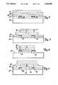
- FIG. 1is an exploded perspective view of an x-ray detector of the present invention.
- FIGS. 2 through 13are sectional views of the process of the present invention forming one pixel unit of the detector array of the present invention.
- FIGS. 14 through 23are sectional views of another embodiment of a pixel unit of an array formed by the process of the present invention.
- the present inventionincludes a process for producing an array of thin-film radiation detectors using a greatly reduced number of microlithography steps.
- one or more layers of a silicon-based substanceare deposited on the substrate.
- silicon-based substanceis meant amorphous silicon, polysilicon, single crystal silicon, or silicon alloys. Silicon alloys include alloys such as silicon nitride, silicon oxide, silicon carbide, and the like.
- a metal layeris then deposited adjacent the layers of silicon-based substance. Selected areas in the metal layer are then removed exposing selected areas of the silicon-based substance layers. Using the metal layer as a mask, the selected areas of the silicon-based substance layers are removed to form the array of sensing devices of the present invention.
- the processis particularly useful in forming an x-ray sensing detector 12 as illustrated in FIG. 1 having a large detection area such as 14 inches by 17 inches.
- the detector 12includes a luminescent layer 14, an array layer 16 of either amorphous silicon Schottky barrier diode, amorphous silicon p-i-n diode, or amorphous silicon photoconductors, or direct x-ray sensors having amorphous selenium wherein luminescent layer 14 is not required, and a polysilicon or single crystal silicon thin-film transistor (TFT) array layer 18.
- the detectorfurther includes real-time read-out circuitry 20.
- the luminescent layer 14converts incident x-rays to corresponding visible light radiation.
- the array 16generates an electrical signal corresponding to the intensity of light from the luminescent layer 14. Current generated in the array 16 is fed to the electrodes of associated TFTs in the array 18.
- the pixels forming such an arrayare typically 85 ⁇ m ⁇ 85 ⁇ m in area. Alignment of the various layers in the TFTs and the array 16, and alignment of the array 16 with respect to the TFTs is essential for a commercially viable device that produces an image with satisfactory resolution. The greater the amount of defective pixels in such a device, the poorer the resolution of the image. In addition, alignment of the layers in each pixel results in an active area in each pixel that is greater than the active areas in pixels produced under prior art methods. The sequence of microlithographic steps that were used in prior art methods resulted in each subsequently formed layer being smaller in area than the layer below in order to minimize alignment problems. Since the process of the present invention automatically aligns the layers as discussed above, the resulting active area of each pixel is greater.
- FIGS. 2 through 13An example of the process of the present invention that produces the sensing device of FIG. 1 is illustrated in FIGS. 2 through 13.
- a metalsuch as chromium is deposited as layer 22 on a coated silicon wafer substrate 24 as illustrated in FIG. 2.
- Other substratessuch as glass, SiO 2 , or quartz, may also be used.
- the chromiumis deposited in a layer approximately 1,000 ⁇ to 3,000 ⁇ thick by sputtering.
- Other metalssuch as tantalum or molybdenum in thicknesses ranging from 1,000 ⁇ to 3,000 ⁇ are also suitable.
- Other metalsmay be deposited by using E-beam evaporation or thermal resistance evaporation.
- n-type doped amorphous silicon(n 30 -a-Si:H) at a thickness of 500 ⁇ .
- the n 30 -a-Si:His deposited preferably using plasma-enhanced chemical vapor deposition (PECVD).
- PECVDplasma-enhanced chemical vapor deposition
- other techniquessuch as low pressure chemical vapor deposition (LPCVD), electron cyclotron resonance chemical vapor deposition (ECRCVD), or sputtering a silicon target in hydrogen and argon atmosphere may also be used.
- a photoresist layer 28is then spin coated on the n 30 -a-Si:H layer, and a conventional microlithographic procedure is then used to form the drain region 30 and source region 32 on the substrate 24 as illustrated in FIG. 3. This microlithographic step is also used to form the source and drain lines and contact pads (not shown).
- an undoped amorphous silicon layer 34(a-Si:H) of 1,000 ⁇ to 5,000 ⁇ in thickness using PECVD is then deposited as illustrated in FIG. 4.
- a dielectric layer 36 of SiN x of 2,000 ⁇is deposited.
- the deposition of SiN xis done through the use of PECVD.
- the dielectric layer 36can also be SiO x or SiN x /SiO x or Ta 2 O 5 and can be formed by either LPCVD, ECRCVD or sputtering.
- a layer 38 of platinum 1,000 ⁇ in thicknessis deposited using conventional sputtering techniques.
- the stacked layers 34, 36, and 38are then annealed using furnace annealing techniques in a nitrogen atmosphere at 600° C. for 15 hours to crystalize the silicon layers and to enhance the dielectric properties of the layer 36.
- the annealingmay also be done using rapid thermal annealing techniques at 600° to 700° C. in an inert atmosphere such as argon or nitrogen for three to 15 minutes.
- E-beam annealing or laser annealingcan also be used.
- a photoresist layer 37is then spin coated on the platinum layer 38 and conventional microlithographic techniques to form a pattern in the platinum layer 38 to remove selective areas of the layer 38.
- the selected areasare preferably removed by sputter-etch in an argon atmosphere.
- the remaining areas of the layers 38 and 37serve as a mask, as best illustrated in FIG. 5, for the removal of selected areas of the dielectric layer 36 and the amorphous silicon layer 34.
- the photoresist layer 37 overlying the layer 38is removed.
- the layers 34, 36, and 38are automatically aligned due to the use of layer 38 as a mask as illustrated in FIG. 6.
- the insulating layer 40is preferably a triple layer containing a first layer 2,000 ⁇ in thickness of SiN x , a second layer 2,000 ⁇ in thickness of SiO x , and a third layer 2,000 ⁇ in thickness of SiN x .
- the thickness of the insulating layermay range from 4,000 ⁇ to 8,000 ⁇ .
- a photoresist layer 42is then deposited on the insulating layer 40 and a microlithographic masking step is then used to open a via hole over each TFT which will subsequently be used to conductively connect the TFTs with the photodiodes in the array, as illustrated in FIG. 8.
- the photodiode 41is formed over the TFT 39, as illustrated in FIG. 9.
- a chromium layer 42 of 1,000 ⁇ thicknessis deposited by sputtering.
- An n-type doped amorphous silicon layer 44 (a-Si:H) of 500 ⁇ thicknessis then deposited using PECVD.
- an undoped amorphous silicon (a-Si:H) layer 46 of 4,000 ⁇ to 5,000 ⁇ thicknessis deposited on the layer 44.
- a platinum layer 48 of 1501/8 thicknessis deposited preferably using known sputter-etch technique on top of the layer 46 to complete the layers forming the photodiode 41.
- a photoresist layer 50is then spin coated on the platinum layer and microlithography is used to pattern the platinum layer, removing selected areas with the remaining areas overlying the TFT 39, as best illustrated in FIG. 10.
- the remaining platinum areas of the layer 48are then used as a mask to remove selected areas of layers 42, 44, 46 to form the photodiode 41, as illustrated in FIG. 11.
- Using the remaining areas of the platinum layer 48 as a maskautomatically aligns remaining areas of layer 42, 44, 46 beneath the platinum layer with the platinum layer.
- prior art techniquesrequired the use of multiple microlithographic steps between the depositions of each layer. Using multiple microlithographic steps required exact alignment of the masking of each layer. Even with exact alignment attempts, defects, such as the top platinum layer 48 and the bottom electrode layer 42 being slightly misaligned can occur causing shorts in the device.
- sputter-etching of the platinum layer 48is preferred, other techniques such as wet etch using aqua regia or lift-off techniques may also be used.
- the n+-type a-Si:H layer 44 and the undoped a-si:H layer 46are etched using preferably reactive ion etching (RIE).
- RIEreactive ion etching
- Wet etch techniquescan also be used.
- Aqua regia etchingis not as preferred as sputter-etching, since aqua regia etching suffers from the disadvantage of attacking other layers and just as quickly or even faster than the platinum.
- Lift-off techniquesgive imprecise etch definition and surface contamination, which results in a device that is somewhat inferior to the one that is made by sputter-etching.
- the photoresist layershould be left on the platinum until the underlying layers have been etched to form the device.
- the photoresisthelps protect the platinum layer 48 during the etching of the underlying layers 44 and 46.
- the layers 44 and 46may be removed by wet or dry etching while the chromium layer 42 is removed by wet etching.
- Platinumis preferred as the top layer for the photodiode.
- platinumcan also be used. Platinum is preferred since it is an inert material and is not easily attacked by etching chemicals, which makes platinum a preferred metal for use as a mask in the process of the present invention.
- X-ray absorptionis a function of Z 5 .
- annealingmay be done in a hydrogen atmosphere at 0.5 to 2 Torr at approximately 300° C. for one to three hours to reduce the defect densities at the platinum/a-Si:H interface. Platinum layers as thick as 300 ⁇ have been used successfully.
- a p-i-n diodemay also be formed over the TFT 39 using the techniques described above instead of a Schottky barrier diode.
- a layer of chromiumapproximately 1,000 ⁇ is deposited over the TFT.
- an n-type doped amorphous silicon layerapproximately 100 ⁇ to 500 ⁇ is deposited on the chromium, with an undoped .amorphous silicon layer approximately 4,000 ⁇ to 5,000 ⁇ deposited on the n-type doped amorphous silicon layer.
- a p-type doped amorphous silicon layeris deposited on the undoped amorphous silicon layer of 100 ⁇ to 500 ⁇ in thickness.
- the p-type doped amorphous siliconcan be amorphous silicon carbide (a-SiC:H).
- An Indium Tin Oxide (ITO) layer of 1,000 ⁇ to 2,000 ⁇is then deposited on the p-type layer.
- the order of the p and n layerscan be reversed.
- the ITO layeris patterned in a similar manner as the platinum layer 48 discussed with respect to the diode 41. After the ITO layer has been patterned and selected areas removed, the ITO layer is then used as a mask to wet or dry-etch the p-i-n or n-i-p layers with the chromium layer being wet-etched last.
- Other materialssuch as amorphous silicon-based alloys, single crystal silicon, copper indium diselenide, and other materials known in the art for photodiodes may also be used.
- a top insulating layer 50is deposited on the diode as illustrated in FIG. 12.
- the insulating layer 50similar to the insulating layer 42, discussed previously, preferably includes a first SiN x layer approximately 2,000 ⁇ , a second SiO x layer of 2,000 ⁇ thickness, and a third SiN x layer of 2,000 ⁇ thickness.
- the layer 50acts as an isolation layer. Microlithography is used to expose the platinum layer 48.
- an aluminum layer 52 doped with one percent silicon of approximately 3,000 ⁇ to 1 ⁇ m in thicknessis deposited on the insulating layer 50 and the platinum layer 48 as illustrated in FIG. 13.
- the layer 52is then masked using microlithography to define a conductive line.
- X-ray sensitive phosphor for use in the detector of the present inventionmay be chosen from those well-known in the radiographic art for use in intensifying screens.
- Such phosphorsinclude gadolinium oxysulfide doped with terbium or europium, yttrium oxide, calcium tungsten, barium, fluorochloride doped with europium, barium sulfate or strontium sulfate doped with terbium or thulium or dysprosium, and zinc sulfide or with cesium iodine doped with thallium.
- the phosphormay be situated individually over each pixel in microcolumns.
- the individual microcolumn arrangementconfines the scattered emitted light to the area of the associated pixel.
- conventional screenscan also be used with the present invention, the use of such a screen results in some spreading of the emitted light which causes a reduction in the image sharpness.
- columnar phosphorresults in greater image sharpness since the emitted light is confined to the column area.
- the thickness of the phosphor layercan be increased without loss in image sharpness. Increasing the thickness of the phosphor provides greater absorption of incident x-rays thereby improving the sensitivity of the detector.
- columnar phosphor layersselected from barium sulfate doped with terbium or thulium or dysprosium, strontium sulfate doped with terbium or thulium or dysprosium and alkali-halide.
- Such phosphor layersmay be formed by vacuum evaporation, sputtering, or other vacuum deposition techniques known in the art.
- Columnar phosphor screens including oxysulfides of gadolinium or lanthanumare described in U.S. Pat. No. 4,069,355.
- Such structured phosphorsare made by vapor deposition techniques.
- Columnar structured phosphorscan also be formed by evaporating cesium iodine doped with thallium on the detector.
- a metal-oxide-semiconductor field effect transistormay be substituted for the thin film transistor to produce the device of the present invention.
- the substratewhich is silicon wafer coated with 1-3 ⁇ m of thermal oxide for insulating
- the silicon layerof 1,000 ⁇ to 15,000 ⁇ in thickness using LPCVD or PECVD.
- Silicon, either in an amorphous state or in a crystalline stateis then annealed using furnace annealing, rapid thermal annealing, E-beam annealing, or laser annealing to form large grain size polycrystalline or single crystal silicon.
- the crystallized silicon layeris then patterned into islands using microlithography.
- a 1,000 ⁇ thickness silicon oxide layer for the gateis grown on the patterned crystallized silicon layer.
- a polysilicon layer of about 1,000 ⁇ to 3,500 ⁇ thickis then deposited by LPCVD.
- the gate oxide and the polysilicon layerare then etched by microlithography. Ion implantation with phosphorous to a level of 10 15 atoms/cm 2 is done to obtain n-type characteristics. After implantation, the phosphorous is activated by annealing between 800° C. to 1,050° C. for 20 minutes.
- a thin layer of 200 ⁇ -500 ⁇ of silicon oxidewas formed on the polysilicon layer due to the activated annealing process.
- via holes for drain and source contactare formed in the silicon oxide. Aluminum doped with one percent silicon is deposited by sputtering to form the drain and source during the same microlithography step using a lift-off technique. Using the process of the present invention, only three microlithography steps are used to form the MOSFET.
- the electrical connection between the photosensitive diode and the TFTmay be done using any one of three alternatives.
- the bottom contact of the photosensing diodeis connected to the TFT gate, or the bottom contact of the photosensing diode is connected to the drain electrode of the TFT, or the top contact of the photosensing diode is connected to the source electrode of the TFT.
- the process of the present inventionmay also be used to form an array radiation detector in which the position of the gate of the TFT is initially deposited on the substrate, as illustrated in FIGS. 14 through 23.
- a metal layer 62 of chromium or tantalum of 1,000 ⁇ to 3,000 ⁇ in thicknessis deposited on a glass substrate 60.
- the glass substratecan be coated with a layer of SiO 2 to prevent contamination of the metal layer such as from sodium leaching from the glass substrate.
- Layer 62can be deposited by sputtering, E-beam evaporation, or thermal resistance evaporation.
- a type photoresist layeris then deposited on the metal layer 62.
- microlithographyis then used to form a gate area 63 from the layer 62.
- a dielectric layer 66 of SiN x of 1,000 ⁇ to 3,000 ⁇ in thickness through the use of PECVDis deposited over the substrate 60 and the gate area 63.
- an a-Si:H undoped layer of 5,000 ⁇ thickness and a phosphorous doped a-Si:H layer 70 500 ⁇ in thicknessis deposited on the layer 68, both layers 68 and 70 being deposited by PECVD.
- a negative photoresist layer 72is then spin coated on the layer 70.
- UV lightas depicted by arrows 75, is used to inhibit the development of the areas not covered by the gate 63 permitting the area of the photoresist behind gate 63 to develop.
- the underlying layers 70 and 68are etched as illustrated in FIG. 17 aligning the layers with the gate area 63. The remainder of the photoresist layer 72 is then removed.
- a metal layer 74 of aluminum doped with one percent silicon of 1,000 ⁇ to 3,000 ⁇is deposited by sputtering, and a photoresist layer 76 is spin coated on the layer 74, as illustrated in FIG. 18.
- a second microlithography stepis used to expose the a-Si:H layer 68 by etching through the metal layer 74 and the doped a-Si:H layer 70 to form a source region 78, a drain region 80 and respective contact lines (not shown).
- the devices forming the arrayare covered with an insulating layer 82 of approximately 6,000 ⁇ of SiN x , as illustrated in FIG. 21.
- a third microlithographic stepis used to form a via hole 84 to the drain region, which is then filled with aluminum doped with one percent silicon 86 and the photoresist (not illustrated) is then removed.
- a bottom electrode 88is then formed in conductive connection to the aluminum silicon plug 86 by depositing a layer (not illustrated) of metal approximately 1,000 ⁇ to 3,000 ⁇ and a layer of photoresist.
- a fourth microlithographic stepis then used to form the bottom electrode 88 of the to-be-formed photoconductor.
- doped and undoped amorphous silicon layers 90are deposited on the insulating layer 82 and on the bottom electrode layer 88.
- a top electrode ITO layer 92 of 1,000 ⁇ to 2,000 ⁇is deposited on the amorphous silicon layers 90 to complete the device.
- the photoconductorcan include amorphous selenium, lead oxide, selenium-telluride, or other selenium-based alloy.
- an insulating layercan be added on top of the photoconductor layer 90 or in between the photoconductor layer 90 and the TFT without requiring a microlithography step.
- polysiliconis specifically mentioned for use in constructing the TFT, other materials, such as cadmium selenide, can also be used.
- the present inventionis not limited to one TFT/one photodiode arrangement or one TFT/photoconductor arrangement for each pixel.
- the pixelcan be structured with adding one or more photodiodes, one or more TFTs and/or one or more capacitors and/or one or more resistors.
- the present inventionis useful for making large area detectors.
- Such large area radiation detectorsare formed by assembling several smaller array containing submodules to create a large module such as 14 inches by 17 inches.
- the submodulesare placed adjacent to each other and are then bonded.
- dead space both physical and electronicis often times created between the submodules.
- the dead space between the bottom electrode of the photoconductor or photodiodeis virtually eliminated.
- the thin film transistoris formed on a substrate of each submodule as described previously.
- the submodulesare then positioned in a side-by-side relationship adjacent each other and the bottom electrode of the photoconductor or photodiode is then deposited over the adjacent submodules and then patterned using microlithography to form the individual bottom electrodes of the photodiode or photoconductor.
- the bottom electrodebonds the submodules together, and provides a common continuous bottom electrode layer for the large area detector.
- On top of the bottom electrodeis deposited the doped and undoped amorphous silicon layers as described previously.
- the top electrodepreferably a platinum layer, is then deposited, and one microlithographic step as described previously is used to form the photoconductor or photodiode, thus forming the large area detector.
Landscapes
- Solid State Image Pick-Up Elements (AREA)
- Measurement Of Radiation (AREA)
- Light Receiving Elements (AREA)
Abstract
Description
The present invention relates to x-ray sensing detectors, in particular, it relates to a process for fabrication of such detectors.
Efforts have been made to replace x-ray film in radiology through the use of x-ray intensifiers, video cameras, displays, and non-film detectors. One such system employs a scintillation crystal to convert x-rays to corresponding visible light radiation, "Digital Slot Radiography Based on a Linear X-Ray Image Intensifier and Two-Dimensional Image Sensors," Beerlage, Levels, and Mulder, SPIE Vol. 626 Medicine, XIV/PACS IV 161-169 (1986). A photodetector is then used to generate an electrical signal corresponding to the intensity of the visible light radiation. The electrical signal from the detector is converted to digital data and stored in a memory device or electrically displayed, such as on a cathode array tube.
Solid state detectors have also been used in x-ray astronomy. One such detector system was reported in "Multi-Element Self-Scanned Mosaic Sensors," Weimer et al, IEEE Spectrum, Mar. 1969, pages 52-65. The system included an array consisting of a matrix of photodiodes which are charged by light to produce electron-hole pairs.
The Catchpole et al U.S. Pat. No. 4,675,739 describes an incident radiation solid state sensing array made of photosensing elements. Each photosensing element includes back-two-back-diodes, one a photo responsive diode and the other a blocking diode. Each of the diodes has an associated capacitance formed by its electrodes. The magnitude of the charge remaining on a given capacitor is sensed and relates back to the intensity of the incident radiation impinging upon the photosensitive diode. Furthermore, in such a linear photodiode array, the scanning time is so long that real time read-out is made impractical. In addition, the linear photodiode array has to be moved to obtain a two-dimensional image.
Another solid state sensing array includes charge-coupled devices. Charge-coupled devices have a layer of relatively conductive semi-conductor material separated from a layer containing electrodes by an insulator in a two-dimensional image sensing array. However, charge-coupled devices can presently be produced at a format of only less than one inch by one inch. Larger formats of arrays have charge transfer problems due to the number of defective devices that can exist in one line of the array. A defective device in one line of the array can result in a charge not being transferred through that line in the array.
The Nishiki et al U.S. Pat. No. 4,689,487 describes the use of a large area solid state detector (40 cm×40 cm). This solid state detector includes pixels in 2,000×2,000 matrix form. Each pixel consists of a photodiode conductively connected in parallel to a capacitor which are both then conductively connected to the drain of a metal oxide semi-conductor field effect transistor (MOSFET). The photodiodes are of a polycrystalline or amorphous silicon material.
The Berger et al U.S. Pat. No. 4,810,881 describes an amorphous silicon detector of 36 cm×43 cm. Each pixel in the detector includes an amorphous silicon diode that is conductively connected in series to a capacitor which in turn are both then conductively connected to the drain of an amorphous silicon-based junction field effect transistor.
In any fabrication process of making large area solid state detectors, the number of microlithography masking steps plays a critical role in determining the yield of usable detector devices, and hence the commercial viability of such devices. Solid state detector devices that include photodiodes and thin-film transistors (TFTs) require a high number of microlithography masking steps. For example, 16 masking steps may be required to produce a DRAM (Dynamic Random Access Memory) device and nine to ten steps to produce a liquid crystal display device. The yield Y for such devices is proportional to Ya, where Y is the yield for each individual masking step, and n is the number of masking steps. The yield may also be defined by Y=e-29AD where A is the chip area and D is the defect density defined as defects per square centimeter. A high number of microlithography steps will cause more defects and large area will create a lowering in yield. Principles of CMOS VLSI Design, Neil Weste, and Kamran Eshraghian, Addison-Wesley Publishing Co., pg. 156. It will be appreciated that the alignment during masking must be exact due to the small area of each pixel, for example, 85 μm×85 μm. Misalignment of the masks can occur easily and result in a short in the device.
The present invention includes a process for producing an array of thin film solid state detectors. The process includes depositing on a substrate one or more layers of a silicon-based substance. A metal layer is then deposited overlying the silicon-based substance layers. An array of metal layer regions is formed in the metal layer by removing selected areas of the metal layer thereby exposing selected layers of the silicon-based substance. Then using the metal layer regions as a mask, selected areas of the silicon-based substance layers are removed to form the array of sensing devices thereby automatically aligning the silicon-based substance layers with the metal layer.
FIG. 1 is an exploded perspective view of an x-ray detector of the present invention.
FIGS. 2 through 13 are sectional views of the process of the present invention forming one pixel unit of the detector array of the present invention.
FIGS. 14 through 23 are sectional views of another embodiment of a pixel unit of an array formed by the process of the present invention.
The present invention includes a process for producing an array of thin-film radiation detectors using a greatly reduced number of microlithography steps. In the process of the present invention, one or more layers of a silicon-based substance are deposited on the substrate. By silicon-based substance is meant amorphous silicon, polysilicon, single crystal silicon, or silicon alloys. Silicon alloys include alloys such as silicon nitride, silicon oxide, silicon carbide, and the like. A metal layer is then deposited adjacent the layers of silicon-based substance. Selected areas in the metal layer are then removed exposing selected areas of the silicon-based substance layers. Using the metal layer as a mask, the selected areas of the silicon-based substance layers are removed to form the array of sensing devices of the present invention.
The process is particularly useful in forming anx-ray sensing detector 12 as illustrated in FIG. 1 having a large detection area such as 14 inches by 17 inches. Thedetector 12 includes aluminescent layer 14, anarray layer 16 of either amorphous silicon Schottky barrier diode, amorphous silicon p-i-n diode, or amorphous silicon photoconductors, or direct x-ray sensors having amorphous selenium whereinluminescent layer 14 is not required, and a polysilicon or single crystal silicon thin-film transistor (TFT)array layer 18. The detector further includes real-time read-outcircuitry 20. Theluminescent layer 14 converts incident x-rays to corresponding visible light radiation. Thearray 16 generates an electrical signal corresponding to the intensity of light from theluminescent layer 14. Current generated in thearray 16 is fed to the electrodes of associated TFTs in thearray 18.
The pixels forming such an array are typically 85 μm×85 μm in area. Alignment of the various layers in the TFTs and thearray 16, and alignment of thearray 16 with respect to the TFTs is essential for a commercially viable device that produces an image with satisfactory resolution. The greater the amount of defective pixels in such a device, the poorer the resolution of the image. In addition, alignment of the layers in each pixel results in an active area in each pixel that is greater than the active areas in pixels produced under prior art methods. The sequence of microlithographic steps that were used in prior art methods resulted in each subsequently formed layer being smaller in area than the layer below in order to minimize alignment problems. Since the process of the present invention automatically aligns the layers as discussed above, the resulting active area of each pixel is greater.
An example of the process of the present invention that produces the sensing device of FIG. 1 is illustrated in FIGS. 2 through 13. First, a metal such as chromium is deposited aslayer 22 on a coatedsilicon wafer substrate 24 as illustrated in FIG. 2. Other substrates, such as glass, SiO2, or quartz, may also be used. The chromium is deposited in a layer approximately 1,000 Å to 3,000 Å thick by sputtering. Other metals such as tantalum or molybdenum in thicknesses ranging from 1,000 Å to 3,000 Å are also suitable. Other metals may be deposited by using E-beam evaporation or thermal resistance evaporation. On top of themetal layer 22 is deposited alayer 26 of n-type doped amorphous silicon (n30 -a-Si:H) at a thickness of 500 Å. The n30 -a-Si:H is deposited preferably using plasma-enhanced chemical vapor deposition (PECVD). However, other techniques such as low pressure chemical vapor deposition (LPCVD), electron cyclotron resonance chemical vapor deposition (ECRCVD), or sputtering a silicon target in hydrogen and argon atmosphere may also be used. Aphotoresist layer 28 is then spin coated on the n30 -a-Si:H layer, and a conventional microlithographic procedure is then used to form thedrain region 30 andsource region 32 on thesubstrate 24 as illustrated in FIG. 3. This microlithographic step is also used to form the source and drain lines and contact pads (not shown).
On the formed drain andsource regions amorphous silicon layer 34, adielectric layer 36 of SiNx of 2,000 Å is deposited. The deposition of SiNx is done through the use of PECVD. Thedielectric layer 36 can also be SiOx or SiNx /SiOx or Ta2 O5 and can be formed by either LPCVD, ECRCVD or sputtering. On the dielectric layer, alayer 38 of platinum 1,000 Å in thickness is deposited using conventional sputtering techniques. Other metals such as tantalum, molybdenum or tungsten ranging from 1,000 Å to 3,000 Å in thickness may also be used. The stacked layers 34, 36, and 38 are then annealed using furnace annealing techniques in a nitrogen atmosphere at 600° C. for 15 hours to crystalize the silicon layers and to enhance the dielectric properties of thelayer 36. The annealing may also be done using rapid thermal annealing techniques at 600° to 700° C. in an inert atmosphere such as argon or nitrogen for three to 15 minutes. Optionally E-beam annealing or laser annealing can also be used.
Aphotoresist layer 37 is then spin coated on theplatinum layer 38 and conventional microlithographic techniques to form a pattern in theplatinum layer 38 to remove selective areas of thelayer 38. The selected areas are preferably removed by sputter-etch in an argon atmosphere. The remaining areas of thelayers dielectric layer 36 and theamorphous silicon layer 34. After removal of the selected areas oflayers photoresist layer 37 overlying thelayer 38 is removed. As can readily be appreciated, thelayers layer 38 as a mask as illustrated in FIG. 6.
Prior to formation of the photodiode, thelayers layer 40, as illustrated in FIG. 7. The insulatinglayer 40 is preferably a triple layer containing a first layer 2,000 Å in thickness of SiNx, a second layer 2,000 Å in thickness of SiOx, and a third layer 2,000 Å in thickness of SiNx. The thickness of the insulating layer may range from 4,000 Å to 8,000 Å.
Aphotoresist layer 42 is then deposited on the insulatinglayer 40 and a microlithographic masking step is then used to open a via hole over each TFT which will subsequently be used to conductively connect the TFTs with the photodiodes in the array, as illustrated in FIG. 8. Next, thephotodiode 41 is formed over theTFT 39, as illustrated in FIG. 9. Achromium layer 42 of 1,000 Å thickness is deposited by sputtering. An n-type doped amorphous silicon layer 44 (a-Si:H) of 500 Å thickness is then deposited using PECVD. Next, an undoped amorphous silicon (a-Si:H)layer 46 of 4,000 Å to 5,000 Å thickness is deposited on thelayer 44. Lastly, aplatinum layer 48 of 1501/8 thickness is deposited preferably using known sputter-etch technique on top of thelayer 46 to complete the layers forming thephotodiode 41.
Aphotoresist layer 50 is then spin coated on the platinum layer and microlithography is used to pattern the platinum layer, removing selected areas with the remaining areas overlying theTFT 39, as best illustrated in FIG. 10. The remaining platinum areas of thelayer 48 are then used as a mask to remove selected areas oflayers photodiode 41, as illustrated in FIG. 11. Using the remaining areas of theplatinum layer 48 as a mask, automatically aligns remaining areas oflayer top platinum layer 48 and thebottom electrode layer 42 being slightly misaligned can occur causing shorts in the device.
Although sputter-etching of theplatinum layer 48 is preferred, other techniques such as wet etch using aqua regia or lift-off techniques may also be used. The n+-type a-Si:H layer 44 and the undoped a-si:H layer 46 are etched using preferably reactive ion etching (RIE). Wet etch techniques can also be used. Aqua regia etching is not as preferred as sputter-etching, since aqua regia etching suffers from the disadvantage of attacking other layers and just as quickly or even faster than the platinum. Lift-off techniques give imprecise etch definition and surface contamination, which results in a device that is somewhat inferior to the one that is made by sputter-etching. In the use of sputter-etching, the photoresist layer should be left on the platinum until the underlying layers have been etched to form the device. The photoresist helps protect theplatinum layer 48 during the etching of theunderlying layers layers chromium layer 42 is removed by wet etching.
Platinum is preferred as the top layer for the photodiode. In addition, although other metals have been mentioned for use in the gate, source, and drain regions of the TFT, platinum can also be used. Platinum is preferred since it is an inert material and is not easily attacked by etching chemicals, which makes platinum a preferred metal for use as a mask in the process of the present invention. In addition, platinum has a very high Z (Z=78), which aids in protecting the layers underneath the platinum layer from x-ray radiation. X-ray absorption is a function of Z5. Metals having Z of at least 73, and preferably 74 or better, aid in x-ray absorption.
After the photodiode has been formed, annealing may be done in a hydrogen atmosphere at 0.5 to 2 Torr at approximately 300° C. for one to three hours to reduce the defect densities at the platinum/a-Si:H interface. Platinum layers as thick as 300 Å have been used successfully.
Alternatively, a p-i-n diode may also be formed over theTFT 39 using the techniques described above instead of a Schottky barrier diode. Initially, a layer of chromium approximately 1,000 Å is deposited over the TFT. Next, an n-type doped amorphous silicon layer approximately 100 Å to 500 Å is deposited on the chromium, with an undoped .amorphous silicon layer approximately 4,000 Å to 5,000 Å deposited on the n-type doped amorphous silicon layer. Next, a p-type doped amorphous silicon layer is deposited on the undoped amorphous silicon layer of 100 Å to 500 Å in thickness. Alternatively, the p-type doped amorphous silicon can be amorphous silicon carbide (a-SiC:H). An Indium Tin Oxide (ITO) layer of 1,000 Å to 2,000 Å is then deposited on the p-type layer. The order of the p and n layers, of course, can be reversed. The ITO layer is patterned in a similar manner as theplatinum layer 48 discussed with respect to thediode 41. After the ITO layer has been patterned and selected areas removed, the ITO layer is then used as a mask to wet or dry-etch the p-i-n or n-i-p layers with the chromium layer being wet-etched last. Other materials such as amorphous silicon-based alloys, single crystal silicon, copper indium diselenide, and other materials known in the art for photodiodes may also be used.
Whether a Schottky barrier diode has been formed or a p-i-n or an n-i-p diode, a top insulatinglayer 50 is deposited on the diode as illustrated in FIG. 12. The insulatinglayer 50 similar to the insulatinglayer 42, discussed previously, preferably includes a first SiNx layer approximately 2,000 Å, a second SiOx layer of 2,000 Å thickness, and a third SiNx layer of 2,000 Å thickness. Thelayer 50 acts as an isolation layer. Microlithography is used to expose theplatinum layer 48.
Next, analuminum layer 52 doped with one percent silicon of approximately 3,000 Å to 1 μm in thickness is deposited on the insulatinglayer 50 and theplatinum layer 48 as illustrated in FIG. 13. Thelayer 52 is then masked using microlithography to define a conductive line.
X-ray sensitive phosphor for use in the detector of the present invention may be chosen from those well-known in the radiographic art for use in intensifying screens. Such phosphors include gadolinium oxysulfide doped with terbium or europium, yttrium oxide, calcium tungsten, barium, fluorochloride doped with europium, barium sulfate or strontium sulfate doped with terbium or thulium or dysprosium, and zinc sulfide or with cesium iodine doped with thallium. The phosphor may be situated individually over each pixel in microcolumns. The individual microcolumn arrangement confines the scattered emitted light to the area of the associated pixel. Although conventional screens can also be used with the present invention, the use of such a screen results in some spreading of the emitted light which causes a reduction in the image sharpness.
The use of columnar phosphor results in greater image sharpness since the emitted light is confined to the column area. In addition, since the scattered emitted light is confined, the thickness of the phosphor layer can be increased without loss in image sharpness. Increasing the thickness of the phosphor provides greater absorption of incident x-rays thereby improving the sensitivity of the detector.
Techniques for producing columnar phosphor are known in the art. European patent application Publication 0 175 578 describes the use of columnar phosphor layers selected from barium sulfate doped with terbium or thulium or dysprosium, strontium sulfate doped with terbium or thulium or dysprosium and alkali-halide. Such phosphor layers may be formed by vacuum evaporation, sputtering, or other vacuum deposition techniques known in the art. Columnar phosphor screens including oxysulfides of gadolinium or lanthanum are described in U.S. Pat. No. 4,069,355. Such structured phosphors are made by vapor deposition techniques. Columnar structured phosphors can also be formed by evaporating cesium iodine doped with thallium on the detector.
A metal-oxide-semiconductor field effect transistor (MOSFET) may be substituted for the thin film transistor to produce the device of the present invention. To produce the MOSFET using the process of the present invention, the substrate (which is silicon wafer coated with 1-3 μm of thermal oxide for insulating) is coated with an silicon layer of 1,000 Å to 15,000 Å in thickness using LPCVD or PECVD. Silicon, either in an amorphous state or in a crystalline state is then annealed using furnace annealing, rapid thermal annealing, E-beam annealing, or laser annealing to form large grain size polycrystalline or single crystal silicon. The crystallized silicon layer is then patterned into islands using microlithography. A 1,000 Å thickness silicon oxide layer for the gate is grown on the patterned crystallized silicon layer. A polysilicon layer of about 1,000 Å to 3,500 Å thick is then deposited by LPCVD. The gate oxide and the polysilicon layer are then etched by microlithography. Ion implantation with phosphorous to a level of 1015 atoms/cm2 is done to obtain n-type characteristics. After implantation, the phosphorous is activated by annealing between 800° C. to 1,050° C. for 20 minutes. A thin layer of 200 Å-500 Å of silicon oxide was formed on the polysilicon layer due to the activated annealing process. Using microlithography, via holes for drain and source contact are formed in the silicon oxide. Aluminum doped with one percent silicon is deposited by sputtering to form the drain and source during the same microlithography step using a lift-off technique. Using the process of the present invention, only three microlithography steps are used to form the MOSFET.
The electrical connection between the photosensitive diode and the TFT may be done using any one of three alternatives. The bottom contact of the photosensing diode is connected to the TFT gate, or the bottom contact of the photosensing diode is connected to the drain electrode of the TFT, or the top contact of the photosensing diode is connected to the source electrode of the TFT.
The process of the present invention may also be used to form an array radiation detector in which the position of the gate of the TFT is initially deposited on the substrate, as illustrated in FIGS. 14 through 23. Initially, ametal layer 62 of chromium or tantalum of 1,000 Å to 3,000 Å in thickness is deposited on aglass substrate 60. Prior to deposition, the glass substrate can be coated with a layer of SiO2 to prevent contamination of the metal layer such as from sodium leaching from the glass substrate.Layer 62 can be deposited by sputtering, E-beam evaporation, or thermal resistance evaporation. A type photoresist layer is then deposited on themetal layer 62. As illustrated in FIG. 15, microlithography is then used to form agate area 63 from thelayer 62.
As next illustrated in FIG. 16, adielectric layer 66 of SiNx of 1,000 Å to 3,000 Å in thickness through the use of PECVD is deposited over thesubstrate 60 and thegate area 63. On top of thedielectric layer 66 is deposited an a-Si:H undoped layer of 5,000 Å thickness and a phosphorous doped a-Si:H layer 70 500 Å in thickness is deposited on thelayer 68, bothlayers negative photoresist layer 72 is then spin coated on thelayer 70. Using thegate electrode area 63 as a mask, UV light, as depicted byarrows 75, is used to inhibit the development of the areas not covered by thegate 63 permitting the area of the photoresist behindgate 63 to develop. Theunderlying layers gate area 63. The remainder of thephotoresist layer 72 is then removed.
Next, ametal layer 74 of aluminum doped with one percent silicon of 1,000 Å to 3,000 Å is deposited by sputtering, and aphotoresist layer 76 is spin coated on thelayer 74, as illustrated in FIG. 18. A second microlithography step is used to expose the a-Si:H layer 68 by etching through themetal layer 74 and the doped a-Si:H layer 70 to form asource region 78, adrain region 80 and respective contact lines (not shown).
Next, after thephotoresist layer 76 has been removed, the devices forming the array are covered with an insulatinglayer 82 of approximately 6,000 Å of SiNx, as illustrated in FIG. 21. A third microlithographic step is used to form a viahole 84 to the drain region, which is then filled with aluminum doped with onepercent silicon 86 and the photoresist (not illustrated) is then removed.
As illustrated in FIG. 22, abottom electrode 88 is then formed in conductive connection to thealuminum silicon plug 86 by depositing a layer (not illustrated) of metal approximately 1,000 Å to 3,000 Å and a layer of photoresist. A fourth microlithographic step is then used to form thebottom electrode 88 of the to-be-formed photoconductor.
Next, doped and undoped amorphous silicon layers 90 are deposited on the insulatinglayer 82 and on thebottom electrode layer 88. A topelectrode ITO layer 92 of 1,000 Å to 2,000 Å is deposited on the amorphous silicon layers 90 to complete the device.
In the photoconductor/TFT structure of FIGS. 14-23, the photoconductor can include amorphous selenium, lead oxide, selenium-telluride, or other selenium-based alloy. As an alternative structure, an insulating layer can be added on top of thephotoconductor layer 90 or in between thephotoconductor layer 90 and the TFT without requiring a microlithography step. Although polysilicon is specifically mentioned for use in constructing the TFT, other materials, such as cadmium selenide, can also be used. The present invention is not limited to one TFT/one photodiode arrangement or one TFT/photoconductor arrangement for each pixel. The pixel can be structured with adding one or more photodiodes, one or more TFTs and/or one or more capacitors and/or one or more resistors.
The present invention is useful for making large area detectors. Such large area radiation detectors are formed by assembling several smaller array containing submodules to create a large module such as 14 inches by 17 inches. In forming the large area modules, the submodules are placed adjacent to each other and are then bonded. However, dead space both physical and electronic is often times created between the submodules. In using the process of the present invention, the dead space between the bottom electrode of the photoconductor or photodiode is virtually eliminated.
First, the thin film transistor is formed on a substrate of each submodule as described previously. The submodules are then positioned in a side-by-side relationship adjacent each other and the bottom electrode of the photoconductor or photodiode is then deposited over the adjacent submodules and then patterned using microlithography to form the individual bottom electrodes of the photodiode or photoconductor. The bottom electrode bonds the submodules together, and provides a common continuous bottom electrode layer for the large area detector. On top of the bottom electrode is deposited the doped and undoped amorphous silicon layers as described previously. The top electrode, preferably a platinum layer, is then deposited, and one microlithographic step as described previously is used to form the photoconductor or photodiode, thus forming the large area detector.
Although the present invention has been described with reference to preferred embodiments, workers skilled in the art will recognize that changes may be made in form and detail without departing from the spirit and scope of the invention.
Claims (8)
1. A process for producing a large area radiation detector, the process comprising:
forming submodules, each submodule including an array of thin film transistors;
positioning the submodules in side-by-side relationship;
forming a bottom electrode layer that overlies the thin film transistor arrays of the submodule;
depositing on the bottom electrode layer doped and undoped amorphous silicon layers;
forming a top electrode layer on the amorphous silicon layers;
using microlithography to form an array of top electrode regions overlying the thin film transistors of the submodules;
selectively etching the doped and undoped amorphous silicon layers using the array of top electrode regions as a mask to form an array of photosensitive devices overlying the thin film transistors
2. The process of claim 1 wherein the photosensitive device is a photodiode.
3. The process of claim 1 wherein the doped amorphous silicon layer includes a p30 -type amorphous silicon layer and an n30 -type amorphous silicon layer.
4. The process of claim 1 wherein the top electrode layer is made of platinum.
5. The process of claim 1 and further including forming an x-ray sensitive phosphor layer in light receiving association with the array of photosensitive devices.
6. A process for producing a large area radiation detector, the process comprising:
forming submodules, each submodule including an array of thin film transistors;
positioning the submodules in side-by-side relationship;
forming a bottom electrode layer that overlies the thin film transistor arrays of the submodules, and patterning the electrode layer using microlithography to form an array of electrodes overlying the array of transistors;
depositing a continuous layer of photoconductor on the bottom electrode layer; and
forming a top common electrode layer on the continuous layer of photoconductor.
7. The process of claim 6 wherein the top common electrode layer is made of platinum.
8. The process of claim 6 and further including forming an x-ray sensitive phosphor layer in light receiving association with the top common electrode layer.
Priority Applications (9)
| Application Number | Priority Date | Filing Date | Title |
|---|---|---|---|
| US07/839,268US5254480A (en) | 1992-02-20 | 1992-02-20 | Process for producing a large area solid state radiation detector |
| CA002087483ACA2087483A1 (en) | 1992-02-20 | 1993-01-18 | Process for producing a solid state radiation detector |
| JP5017209AJPH05283664A (en) | 1992-02-20 | 1993-02-04 | Method of manufacturing solid-state radiation detector |
| EP97113907AEP0814503A3 (en) | 1992-02-20 | 1993-02-18 | Solid state radiation detector |
| EP93102547AEP0556820A1 (en) | 1992-02-20 | 1993-02-18 | Process for producing a solid state radiation detector |
| US08/383,070US5525527A (en) | 1992-02-20 | 1995-02-03 | Process for producing a solid state radiation detector |
| US08/658,394US5818053A (en) | 1992-02-20 | 1996-06-05 | Multi-module solid state radiation detector with continuous photoconductor layer and fabrication method |
| US08/962,626US5942756A (en) | 1992-02-20 | 1997-11-03 | Radiation detector and fabrication method |
| US09/551,482US6262421B1 (en) | 1992-02-20 | 2000-04-18 | Solid state radiation detector for x-ray imaging |
Applications Claiming Priority (1)
| Application Number | Priority Date | Filing Date | Title |
|---|---|---|---|
| US07/839,268US5254480A (en) | 1992-02-20 | 1992-02-20 | Process for producing a large area solid state radiation detector |
Related Child Applications (1)
| Application Number | Title | Priority Date | Filing Date |
|---|---|---|---|
| US6893393ADivision | 1992-02-20 | 1993-05-27 |
Publications (1)
| Publication Number | Publication Date |
|---|---|
| US5254480Atrue US5254480A (en) | 1993-10-19 |
Family
ID=25279285
Family Applications (5)
| Application Number | Title | Priority Date | Filing Date |
|---|---|---|---|
| US07/839,268Expired - LifetimeUS5254480A (en) | 1992-02-20 | 1992-02-20 | Process for producing a large area solid state radiation detector |
| US08/383,070Expired - LifetimeUS5525527A (en) | 1992-02-20 | 1995-02-03 | Process for producing a solid state radiation detector |
| US08/658,394Expired - Fee RelatedUS5818053A (en) | 1992-02-20 | 1996-06-05 | Multi-module solid state radiation detector with continuous photoconductor layer and fabrication method |
| US08/962,626Expired - LifetimeUS5942756A (en) | 1992-02-20 | 1997-11-03 | Radiation detector and fabrication method |
| US09/551,482Expired - Fee RelatedUS6262421B1 (en) | 1992-02-20 | 2000-04-18 | Solid state radiation detector for x-ray imaging |
Family Applications After (4)
| Application Number | Title | Priority Date | Filing Date |
|---|---|---|---|
| US08/383,070Expired - LifetimeUS5525527A (en) | 1992-02-20 | 1995-02-03 | Process for producing a solid state radiation detector |
| US08/658,394Expired - Fee RelatedUS5818053A (en) | 1992-02-20 | 1996-06-05 | Multi-module solid state radiation detector with continuous photoconductor layer and fabrication method |
| US08/962,626Expired - LifetimeUS5942756A (en) | 1992-02-20 | 1997-11-03 | Radiation detector and fabrication method |
| US09/551,482Expired - Fee RelatedUS6262421B1 (en) | 1992-02-20 | 2000-04-18 | Solid state radiation detector for x-ray imaging |
Country Status (4)
| Country | Link |
|---|---|
| US (5) | US5254480A (en) |
| EP (2) | EP0556820A1 (en) |
| JP (1) | JPH05283664A (en) |
| CA (1) | CA2087483A1 (en) |
Cited By (80)
| Publication number | Priority date | Publication date | Assignee | Title |
|---|---|---|---|---|
| US5332686A (en)* | 1991-10-22 | 1994-07-26 | Florida Atlantic University | Method of manufacturing large capacity solid-state memory |
| US5381014A (en)* | 1993-12-29 | 1995-01-10 | E. I. Du Pont De Nemours And Company | Large area X-ray imager and method of fabrication |
| US5462898A (en)* | 1994-05-25 | 1995-10-31 | Georgia Tech Research Corporation | Methods for passivating silicon devices at low temperature to achieve low interface state density and low recombination velocity while preserving carrier lifetime |
| US5482896A (en)* | 1993-11-18 | 1996-01-09 | Eastman Kodak Company | Light emitting device comprising an organic LED array on an ultra thin substrate and process for forming same |
| US5498880A (en)* | 1995-01-12 | 1996-03-12 | E. I. Du Pont De Nemours And Company | Image capture panel using a solid state device |
| US5525527A (en)* | 1992-02-20 | 1996-06-11 | Minnesota Mining And Manufacturing Company | Process for producing a solid state radiation detector |
| US5529937A (en)* | 1993-07-27 | 1996-06-25 | Semiconductor Energy Laboratory Co., Ltd. | Process for fabricating thin film transistor |
| US5563421A (en)* | 1995-06-07 | 1996-10-08 | Sterling Diagnostic Imaging, Inc. | Apparatus and method for eliminating residual charges in an image capture panel |
| US5574293A (en)* | 1993-03-23 | 1996-11-12 | Tdk Corp. | Solid state imaging device using disilane |
| US5576239A (en)* | 1994-05-31 | 1996-11-19 | Nec Corporation | Method of manufacturing solid state image sensing device |
| US5585280A (en)* | 1992-06-01 | 1996-12-17 | General Electric Company | Method of fabricating solid state radiation imager with high integrity barrier layer |
| US5585638A (en)* | 1995-12-14 | 1996-12-17 | General Electric Company | X-ray detector for automatic exposure control of an imaging apparatus |
| US5629968A (en)* | 1995-05-12 | 1997-05-13 | Eastman Kodak Company | Apparatus and method for obtaining two radiographic images of an object from one exposing radiation dose |
| US5635718A (en)* | 1996-01-16 | 1997-06-03 | Minnesota Mining And Manufacturing Company | Multi-module radiation detecting device and fabrication method |
| US5650626A (en)* | 1996-07-16 | 1997-07-22 | Eastman Kodak Company | X-ray imaging detector with thickness and composition limited substrate |
| US5652430A (en)* | 1996-05-03 | 1997-07-29 | Sterling Diagnostic Imaging, Inc. | Direct radiographic imaging panel |
| US5693947A (en)* | 1993-04-28 | 1997-12-02 | The University Of Surrey | Radiation detectors |
| WO1997048988A1 (en)* | 1996-06-18 | 1997-12-24 | Thermotrex Corp. | Imaging device |
| US5753921A (en)* | 1996-07-16 | 1998-05-19 | Eastman Kodak Company | X-ray imaging detector with limited substrate and converter |
| US5789276A (en)* | 1995-01-12 | 1998-08-04 | International Business Machines Corporation | Optical FET |
| US5847499A (en)* | 1997-01-31 | 1998-12-08 | Sunnybrook Hospital | Apparatus for generating multiple X-ray images of an object from a single X-ray exposure |
| US5869837A (en)* | 1994-07-27 | 1999-02-09 | Litton Systems Canada Limited | Radiation imaging panel |
| US5886359A (en)* | 1996-06-13 | 1999-03-23 | Eastman Kodak Company | X-ray dectector, detection assembly, and method |
| US5946560A (en)* | 1993-03-22 | 1999-08-31 | Semiconductor Energy Laboratory Co., Ltd. | Transistor and method of forming the same |
| US5973311A (en)* | 1997-02-12 | 1999-10-26 | Imation Corp | Pixel array with high and low resolution mode |
| US5982460A (en)* | 1996-06-25 | 1999-11-09 | Semiconductor Energy Laboratory Co., Ltd. | Electro-optical display |
| US5985700A (en)* | 1996-11-26 | 1999-11-16 | Corning Incorporated | TFT fabrication on leached glass surface |
| US6025599A (en)* | 1997-12-09 | 2000-02-15 | Direct Radiography Corp. | Image capture element |
| US6043552A (en)* | 1996-11-05 | 2000-03-28 | Sony Corporation | Semiconductor device and method of manufacturing the semiconductor device |
| WO2000031522A1 (en) | 1998-11-20 | 2000-06-02 | Direct Radiography Corp | Interactive digital radiographic system |
| US6072193A (en)* | 1997-05-30 | 2000-06-06 | Semiconductor Energy Laboratory Co., Ltd. | Thin-film transistor and semiconductor device using thin-film transistors |
| US6075248A (en)* | 1998-10-22 | 2000-06-13 | Direct Radiography Corp. | Direct radiographic imaging panel with shielding electrode |
| US6115088A (en)* | 1996-09-04 | 2000-09-05 | Semiconductor Energy Laboratory Co., Ltd. | Display device |
| US6140165A (en)* | 1993-03-12 | 2000-10-31 | Semiconductor Energy Laboratory Co., Ltd. | Semiconductor device forming method |
| US6180944B1 (en) | 1998-07-07 | 2001-01-30 | Direct Radiography, Corp. | Large area X-ray imager with vented seam and method of fabrication |
| US6180439B1 (en) | 1996-01-26 | 2001-01-30 | Semiconductor Energy Laboratory Co., Ltd. | Method for fabricating a semiconductor device |
| US6225152B1 (en) | 1996-01-20 | 2001-05-01 | Semiconductor Energy Laboratory Co., Ltd. | Semiconductor device and fabrication method thereof |
| US6232607B1 (en) | 1996-05-08 | 2001-05-15 | Ifire Technology Inc. | High resolution flat panel for radiation imaging |
| WO2001035085A1 (en) | 1999-11-12 | 2001-05-17 | Direct Radiography Corp. | Digital image orientation marker |
| US6300659B1 (en) | 1994-09-30 | 2001-10-09 | Semiconductor Energy Laboratory Co., Ltd. | Thin-film transistor and fabrication method for same |
| US6316810B1 (en) | 1996-01-19 | 2001-11-13 | Semiconductor Energy Laboratory Co., Ltd. | Display switch with double layered gate insulation and resinous interlayer dielectric |
| US6319761B1 (en) | 1993-06-22 | 2001-11-20 | Semiconductor Energy Laboratory Co., Ltd. | Method of fabricating a thin film transistor |
| US6350985B1 (en) | 1999-04-26 | 2002-02-26 | Direct Radiography Corp. | Method for calculating gain correction factors in a digital imaging system |
| US6465287B1 (en) | 1996-01-27 | 2002-10-15 | Semiconductor Energy Laboratory Co., Ltd. | Method for fabricating a semiconductor device using a metal catalyst and high temperature crystallization |
| US6475840B1 (en) | 1993-06-12 | 2002-11-05 | Semiconductor Energy Laboratory Co., Ltd. | Semiconductor device and method for manufacturing the same |
| US6478263B1 (en) | 1997-01-17 | 2002-11-12 | Semiconductor Energy Laboratory Co., Ltd. | Semiconductor device and its manufacturing method |
| US6486470B2 (en) | 1998-11-02 | 2002-11-26 | 1294339 Ontario, Inc. | Compensation circuit for use in a high resolution amplified flat panel for radiation imaging |
| US6504174B1 (en) | 1996-01-19 | 2003-01-07 | Semiconductor Energy Laboratory Co., Ltd. | Semiconductor device and method for fabricating the same |
| US6528820B1 (en) | 1996-01-19 | 2003-03-04 | Semiconductor Energy Laboratory Co., Ltd. | Semiconductor device and method of fabricating same |
| US6541793B2 (en) | 1997-05-30 | 2003-04-01 | Semiconductor Energy Laboratory Co., Ltd. | Thin-film transistor and semiconductor device using thin-film transistors |
| US6653176B2 (en) | 2001-12-22 | 2003-11-25 | Boe-Hydis Technology Co., Ltd. | Method for manufacturing x-ray detector |
| US6679997B2 (en)* | 1998-08-12 | 2004-01-20 | Nec Compound Semiconductor Devices, Ltd. | Organic insulation film formation method |
| US6713330B1 (en) | 1993-06-22 | 2004-03-30 | Semiconductor Energy Laboratory Co., Ltd. | Method of fabricating a thin film transistor |
| US6744069B1 (en) | 1996-01-19 | 2004-06-01 | Semiconductor Energy Laboratory Co., Ltd. | Semiconductor device and its manufacturing method |
| US20040232491A1 (en)* | 1993-12-22 | 2004-11-25 | Semiconductor Energy Laboratory Co., Ltd. | Semiconductor device and method for manufacturing the same |
| US7056381B1 (en) | 1996-01-26 | 2006-06-06 | Semiconductor Energy Laboratory Co., Ltd. | Fabrication method of semiconductor device |
| US7135741B1 (en) | 1996-03-17 | 2006-11-14 | Semiconductor Energy Laboratory Co., Ltd. | Method of manufacturing a semiconductor device |
| US20060255420A1 (en)* | 2003-05-05 | 2006-11-16 | Bui Peter S | Front illuminated back side contact thin wafer detectors |
| US20060274297A1 (en)* | 2005-06-02 | 2006-12-07 | Canon Kabushiki Kaisha | Photo detector unit and exposure apparatus having the same |
| US20070228469A1 (en)* | 2004-03-23 | 2007-10-04 | Fumiki Nakano | Thin-film transistor formed on insulating substrate |
| US20070278534A1 (en)* | 2006-06-05 | 2007-12-06 | Peter Steven Bui | Low crosstalk, front-side illuminated, back-side contact photodiode array |
| US20080099871A1 (en)* | 2006-11-01 | 2008-05-01 | Peter Steven Bui | Front-side illuminated, back-side contact double-sided pn-junction photodiode arrays |
| US20080128846A1 (en)* | 2003-05-05 | 2008-06-05 | Udt Sensors, Inc. | Thin wafer detectors with improved radiation damage and crosstalk characteristics |
| US20090140366A1 (en)* | 2005-03-16 | 2009-06-04 | Peter Steven Bui | Photodiode with Controlled Current Leakage |
| US7576369B2 (en) | 2005-10-25 | 2009-08-18 | Udt Sensors, Inc. | Deep diffused thin photodiodes |
| US7655999B2 (en) | 2006-09-15 | 2010-02-02 | Udt Sensors, Inc. | High density photodiodes |
| US20100053802A1 (en)* | 2008-08-27 | 2010-03-04 | Masaki Yamashita | Low Power Disk-Drive Motor Driver |
| US7709921B2 (en) | 2008-08-27 | 2010-05-04 | Udt Sensors, Inc. | Photodiode and photodiode array with improved performance characteristics |
| US7709837B2 (en) | 1996-01-19 | 2010-05-04 | Semiconductor Energy Laboratory Co., Ltd | Semiconductor device and its manufacturing method |
| US20100264505A1 (en)* | 2003-05-05 | 2010-10-21 | Peter Steven Bui | Photodiodes with PN Junction on Both Front and Back Sides |
| US20100289105A1 (en)* | 2006-05-15 | 2010-11-18 | Peter Steven Bui | Edge Illuminated Photodiodes |
| US20100308371A1 (en)* | 2009-05-12 | 2010-12-09 | Peter Steven Bui | Tetra-Lateral Position Sensing Detector |
| US20110175188A1 (en)* | 2010-01-19 | 2011-07-21 | Peter Steven Bui | Wavelength Sensitive Sensor Photodiodes |
| US20120080607A1 (en)* | 2009-06-12 | 2012-04-05 | Karim Sallaudin Karim | Radiation detector with integrated readout |
| US8907440B2 (en) | 2003-05-05 | 2014-12-09 | Osi Optoelectronics, Inc. | High speed backside illuminated, front side contact photodiode array |
| US8912615B2 (en) | 2013-01-24 | 2014-12-16 | Osi Optoelectronics, Inc. | Shallow junction photodiode for detecting short wavelength light |
| US9035412B2 (en) | 2007-05-07 | 2015-05-19 | Osi Optoelectronics, Inc. | Thin active layer fishbone photodiode with a shallow N+ layer and method of manufacturing the same |
| US9178092B2 (en) | 2006-11-01 | 2015-11-03 | Osi Optoelectronics, Inc. | Front-side illuminated, back-side contact double-sided PN-junction photodiode arrays |
| US10254417B2 (en)* | 2015-11-19 | 2019-04-09 | Shimadzu Corporation | Semiconductor detector |
| US20200273664A1 (en)* | 2019-02-26 | 2020-08-27 | Asml Netherlands B.V. | Charged particle detector with gain element |
Families Citing this family (64)
| Publication number | Priority date | Publication date | Assignee | Title |
|---|---|---|---|---|
| US5640563A (en)* | 1992-01-31 | 1997-06-17 | International Business Machines Corporation | Multi-media computer operating system and method |
| JP3066944B2 (en)* | 1993-12-27 | 2000-07-17 | キヤノン株式会社 | Photoelectric conversion device, driving method thereof, and system having the same |
| GB2289983B (en) | 1994-06-01 | 1996-10-16 | Simage Oy | Imaging devices,systems and methods |
| US5567971A (en)* | 1995-06-07 | 1996-10-22 | Xerox Corporation | Variable size light sensor element |
| GB9520791D0 (en)* | 1995-10-13 | 1995-12-13 | Philips Electronics Nv | Image sensor |
| JP3409542B2 (en)* | 1995-11-21 | 2003-05-26 | ソニー株式会社 | Method for manufacturing semiconductor device |
| US5859463A (en)* | 1996-12-23 | 1999-01-12 | General Electric Company | Photosensitive imager contact pad structure |
| US6013916A (en)* | 1997-07-23 | 2000-01-11 | The Regents Of The University Of Michigan | Flat panel dosimeter |
| IL123006A (en) | 1998-01-20 | 2005-12-18 | Edge Medical Devices Ltd | X-ray imaging system |
| US5994157A (en)* | 1998-01-22 | 1999-11-30 | Ois Optical Imaging Systems, Inc. | Method of making a large area imager with UV Blocking layer, and corresponding imager |
| KR100590742B1 (en)* | 1998-05-11 | 2007-04-25 | 삼성전자주식회사 | Manufacturing method of thin film transistor substrate for liquid crystal display device |
| IL126018A0 (en) | 1998-09-01 | 1999-05-09 | Edge Medical Devices Ltd | X-ray imaging system |
| US9029793B2 (en) | 1998-11-05 | 2015-05-12 | Siemens Aktiengesellschaft | Imaging device |
| US6326625B1 (en) | 1999-01-20 | 2001-12-04 | Edge Medical Devices Ltd. | X-ray imaging system |
| WO2000049840A1 (en)* | 1999-02-19 | 2000-08-24 | The Research Foundation Of State University Of New York | Radiographic imaging apparatus and method for vascular interventions |
| US6178225B1 (en) | 1999-06-04 | 2001-01-23 | Edge Medical Devices Ltd. | System and method for management of X-ray imaging facilities |
| KR100299537B1 (en)* | 1999-08-31 | 2001-11-01 | 남상희 | Fabricating Method of Thin Film Transistor Substrate For Detecting X-ray |
| US7538325B2 (en)* | 2000-02-10 | 2009-05-26 | American Science And Engineering, Inc. | Single-pulse-switched multiple energy X-ray source applications |
| US20030165211A1 (en)* | 2002-03-01 | 2003-09-04 | Lee Grodzins | Detectors for x-rays and neutrons |
| US20050117683A1 (en)* | 2000-02-10 | 2005-06-02 | Andrey Mishin | Multiple energy x-ray source for security applications |
| US20050105665A1 (en)* | 2000-03-28 | 2005-05-19 | Lee Grodzins | Detection of neutrons and sources of radioactive material |
| US8325871B2 (en) | 2000-03-28 | 2012-12-04 | American Science And Engineering, Inc. | Radiation threat detection |
| US7902546B2 (en)* | 2000-08-08 | 2011-03-08 | Translucent, Inc. | Rare earth-oxides, rare earth -nitrides, rare earth -phosphides and ternary alloys with silicon |
| JP4511092B2 (en)* | 2000-12-11 | 2010-07-28 | セイコーエプソン株式会社 | Manufacturing method of semiconductor device |
| JP2002333848A (en)* | 2001-05-10 | 2002-11-22 | Sharp Corp | Composite active matrix substrate, method of manufacturing the same, and electromagnetic wave imaging device |
| US6601276B2 (en) | 2001-05-11 | 2003-08-05 | Agere Systems Inc. | Method for self alignment of patterned layers in thin film acoustic devices |
| US6780786B2 (en)* | 2001-11-26 | 2004-08-24 | The Regents Of The University Of California | Method for producing a porous silicon film |
| US6740884B2 (en)* | 2002-04-03 | 2004-05-25 | General Electric Company | Imaging array and methods for fabricating same |
| US6559506B1 (en) | 2002-04-03 | 2003-05-06 | General Electric Company | Imaging array and methods for fabricating same |
| US6777685B2 (en)* | 2002-04-03 | 2004-08-17 | General Electric Company | Imaging array and methods for fabricating same |
| US7339187B2 (en)* | 2002-05-21 | 2008-03-04 | State Of Oregon Acting By And Through The Oregon State Board Of Higher Education On Behalf Of Oregon State University | Transistor structures |
| US7189992B2 (en)* | 2002-05-21 | 2007-03-13 | State Of Oregon Acting By And Through The Oregon State Board Of Higher Education On Behalf Of Oregon State University | Transistor structures having a transparent channel |
| US7214945B2 (en) | 2002-06-11 | 2007-05-08 | Canon Kabushiki Kaisha | Radiation detecting apparatus, manufacturing method therefor, and radiation image pickup system |
| TW544946B (en)* | 2002-07-12 | 2003-08-01 | Hannstar Display Corp | Manufacturing method of X-ray inspecting instrument array unit |
| US20040061058A1 (en)* | 2002-09-30 | 2004-04-01 | Williams James Richard | Scintillation detector with gadolinium based sidewall axial restraint and compliance assembly |
| US7067843B2 (en)* | 2002-10-11 | 2006-06-27 | E. I. Du Pont De Nemours And Company | Transparent oxide semiconductor thin film transistors |
| GB0224689D0 (en) | 2002-10-23 | 2002-12-04 | Simage Oy | Formation of contacts on semiconductor substrates |
| AU2003276401A1 (en)* | 2002-10-25 | 2004-05-13 | Goldpower Limited | Circuit substrate and method |
| US20040146138A1 (en)* | 2003-01-23 | 2004-07-29 | Motorola, Inc. | Large flat panel gallium arsenide arrays on silicon substrate for low dose X-ray digital imaging |
| US6979838B2 (en)* | 2003-09-03 | 2005-12-27 | Hewlett-Packard Development Company, L.P. | Ultra-high density storage device using phase change diode memory cells and methods of fabrication thereof |
| US7057202B2 (en)* | 2003-09-26 | 2006-06-06 | Hewlett-Packard Development Company, L.P. | Ultra-high density storage device using phase change diode memory cells and methods of fabrication thereof |
| US7773404B2 (en) | 2005-01-07 | 2010-08-10 | Invisage Technologies, Inc. | Quantum dot optical devices with enhanced gain and sensitivity and methods of making same |
| US7746681B2 (en) | 2005-01-07 | 2010-06-29 | Invisage Technologies, Inc. | Methods of making quantum dot films |
| US7742322B2 (en) | 2005-01-07 | 2010-06-22 | Invisage Technologies, Inc. | Electronic and optoelectronic devices with quantum dot films |
| WO2005101530A1 (en) | 2004-04-19 | 2005-10-27 | Edward Sargent | Optically-regulated optical emission using colloidal quantum dot nanocrystals |
| JP4266898B2 (en)* | 2004-08-10 | 2009-05-20 | キヤノン株式会社 | Radiation detection apparatus, manufacturing method thereof, and radiation imaging system |
| EP1836792A1 (en)* | 2004-12-30 | 2007-09-26 | BCE Inc. | System and method for secure access |
| CA2519608A1 (en) | 2005-01-07 | 2006-07-07 | Edward Sargent | Quantum dot-polymer nanocomposite photodetectors and photovoltaics |
| US7671342B2 (en)* | 2005-01-11 | 2010-03-02 | Siemens Medical Solutions Usa, Inc. | Multi-layer detector and method for imaging |
| US7304308B2 (en)* | 2005-02-16 | 2007-12-04 | Hologic, Inc. | Amorphous selenium flat panel x-ray imager for tomosynthesis and static imaging |
| US7233005B2 (en)* | 2005-02-16 | 2007-06-19 | Hologic, Inc. | Amorphous selenium flat panel x-ray imager for tomosynthesis and static imaging |
| US7122803B2 (en)* | 2005-02-16 | 2006-10-17 | Hologic, Inc. | Amorphous selenium flat panel x-ray imager for tomosynthesis and static imaging |
| JP4986923B2 (en)* | 2008-05-07 | 2012-07-25 | 株式会社半導体エネルギー研究所 | Image sensor fabrication method |
| US8483008B2 (en)* | 2008-11-08 | 2013-07-09 | Westerngeco L.L.C. | Coil shooting mode |
| KR101016070B1 (en)* | 2009-02-13 | 2011-02-17 | 경북대학교 산학협력단 | Double sided silicon strip sensor for radiation detection and manufacturing method thereof |
| CN102443391B (en)* | 2010-09-30 | 2014-07-16 | 奇美实业股份有限公司 | Method for controlling ratio of structural components of fired phosphor, and light-emitting device |
| US9935152B2 (en) | 2012-12-27 | 2018-04-03 | General Electric Company | X-ray detector having improved noise performance |
| US9917133B2 (en) | 2013-12-12 | 2018-03-13 | General Electric Company | Optoelectronic device with flexible substrate |
| WO2015138329A1 (en) | 2014-03-13 | 2015-09-17 | General Electric Company | Curved digital x-ray detector for weld inspection |
| US9559236B2 (en)* | 2014-09-24 | 2017-01-31 | Sunpower Corporation | Solar cell fabricated by simplified deposition process |
| US9599723B2 (en) | 2015-08-18 | 2017-03-21 | Carestream Health, Inc. | Method and apparatus with tiled image sensors |
| US10686003B2 (en)* | 2015-12-31 | 2020-06-16 | General Electric Company | Radiation detector assembly |
| AR104999A1 (en) | 2016-06-14 | 2017-08-30 | Consejo Nac De Investig Científicas Y Técnicas (Conicet) | DETECTOR OF THERMAL AND SUB-THERMAL NEUTRONS OF HIGH SPACE RESOLUTION IN TWO DIMENSIONS BASED ON CCD AND CMOS ELECTRONIC SENSORS AND A CONVERSOR CONTAINING GADOLINUM |
| CN108198178B (en)* | 2018-01-02 | 2020-04-28 | 石家庄学院 | Method and device for determining atmospheric range radiation value |
Citations (33)
| Publication number | Priority date | Publication date | Assignee | Title |
|---|---|---|---|---|
| US3825763A (en)* | 1971-07-10 | 1974-07-23 | Philips Corp | Luminescent screen having a mosaic structure |
| US4069355A (en)* | 1975-04-28 | 1978-01-17 | General Electric Company | Process of making structured x-ray phosphor screen |
| US4226898A (en)* | 1978-03-16 | 1980-10-07 | Energy Conversion Devices, Inc. | Amorphous semiconductors equivalent to crystalline semiconductors produced by a glow discharge process |
| JPS6016462A (en)* | 1983-07-08 | 1985-01-28 | Seiko Epson Corp | Manufacturing method of semiconductor device |
| US4511799A (en)* | 1982-12-10 | 1985-04-16 | American Science And Engineering, Inc. | Dual energy imaging |
| US4543490A (en)* | 1983-08-15 | 1985-09-24 | Tokyo Shibaura Denki Kabushiki Kaisha | High density detector array with replaceable sections |
| US4608749A (en)* | 1983-08-23 | 1986-09-02 | Kabushiki Kaisha Toshiba | Method of manufacturing a solid-state image pickup device |
| JPS6251264A (en)* | 1985-08-30 | 1987-03-05 | Hitachi Ltd | Manufcture of thin film transistor |
| US4672454A (en)* | 1984-05-04 | 1987-06-09 | Energy Conversion Devices, Inc. | X-ray image scanner and method |
| US4675739A (en)* | 1984-05-04 | 1987-06-23 | Energy Conversion Devices, Inc. | Integrated radiation sensing array |
| US4689487A (en)* | 1984-09-03 | 1987-08-25 | Kabushiki Kaisha Toshiba | Radiographic image detection apparatus |
| US4735908A (en)* | 1984-10-22 | 1988-04-05 | Fuji Photo Film Co., Ltd. | Process for fabricating solid-state imaging device |
| US4769338A (en)* | 1984-05-14 | 1988-09-06 | Energy Conversion Devices, Inc. | Thin film field effect transistor and method of making same |
| JPS63261880A (en)* | 1987-04-20 | 1988-10-28 | Seiko Epson Corp | Manufacturing method of thin film transistor |
| US4788582A (en)* | 1982-12-16 | 1988-11-29 | Hitachi, Ltd. | Semiconductor device and method of manufacturing the same |
| US4799094A (en)* | 1984-12-27 | 1989-01-17 | Thomson-Csf | Large-format photosensitive device and a method of utilization |
| US4810881A (en)* | 1986-04-30 | 1989-03-07 | Thomson-Csf | Panel for X-ray photography and method of manufacture |
| JPS6461062A (en)* | 1987-09-01 | 1989-03-08 | Ricoh Kk | Manufacture of thin film transistor |
| US4859617A (en)* | 1987-06-09 | 1989-08-22 | Oki Electric Industry Co., Ltd. | Thin-film transistor fabrication process |
| US4866003A (en)* | 1986-11-22 | 1989-09-12 | Yamaha Corporation | Plasma vapor deposition of an improved passivation film using electron cyclotron resonance |
| US4883766A (en)* | 1987-11-14 | 1989-11-28 | Ricoh Company, Ltd. | Method of producing thin film transistor |
| JPH0282578A (en)* | 1988-09-19 | 1990-03-23 | Seiko Epson Corp | Manufacturing method of thin film transistor |
| US4940901A (en)* | 1987-11-10 | 1990-07-10 | Thomson-Csf | X-ray imaging device |
| US4943837A (en)* | 1987-03-11 | 1990-07-24 | Hitachi, Ltd. | Thin film semiconductor device and method of fabricating the same |
| US4954706A (en)* | 1988-04-01 | 1990-09-04 | Hitachi, Ltd. | Radiographic image pickup apparatus |
| US4980553A (en)* | 1988-05-03 | 1990-12-25 | Thomson-Csf | Radiological image detector |
| EP0175578B1 (en)* | 1984-09-18 | 1990-12-27 | Konica Corporation | Radiographic image storage panel and its preparing process |
| US4982095A (en)* | 1987-09-04 | 1991-01-01 | Hitachi, Ltd. | Multi-element type radiation detector |
| EP0441521A1 (en)* | 1990-02-09 | 1991-08-14 | Minnesota Mining And Manufacturing Company | Solid state X-ray imaging device |
| US5079426A (en)* | 1989-09-06 | 1992-01-07 | The Regents Of The University Of Michigan | Multi-element-amorphous-silicon-detector-array for real-time imaging and dosimetry of megavoltage photons and diagnostic X rays |
| WO1992002959A1 (en)* | 1990-08-08 | 1992-02-20 | Minnesota Mining And Manufacturing Company | Solid state electromagnetic radiation detector |
| US5132541A (en)* | 1990-01-27 | 1992-07-21 | U.S. Philips Corporation | Sensor matrix |
| US5187369A (en)* | 1990-10-01 | 1993-02-16 | General Electric Company | High sensitivity, high resolution, solid state x-ray imaging device with barrier layer |
Family Cites Families (25)
| Publication number | Priority date | Publication date | Assignee | Title |
|---|---|---|---|---|
| US4129848A (en)* | 1975-09-03 | 1978-12-12 | Raytheon Company | Platinum film resistor device |
| US4467342A (en)* | 1982-07-15 | 1984-08-21 | Rca Corporation | Multi-chip imager |
| US4929569A (en)* | 1984-01-23 | 1990-05-29 | Ovonic Imaging Systems, Inc. | Method of fabricating amorphous silican diode addressed liquid crystal display |
| US5043582A (en)* | 1985-12-11 | 1991-08-27 | General Imagining Corporation | X-ray imaging system and solid state detector therefor |
| US5220170A (en)* | 1985-12-11 | 1993-06-15 | General Imaging Corporation | X-ray imaging system and solid state detector therefor |
| JPS62291067A (en)* | 1986-06-10 | 1987-12-17 | Nec Corp | Manufacture of thin film transistor |
| JPS63210231A (en)* | 1987-02-26 | 1988-08-31 | Nippon Steel Corp | Furnace wall lining structure |
| KR910009039B1 (en)* | 1987-12-18 | 1991-10-28 | 가부시끼가이샤 세이꼬오샤 | Method for manufacturing amorphous silicon thin film transistor |
| JPH0242761A (en)* | 1988-04-20 | 1990-02-13 | Matsushita Electric Ind Co Ltd | Active matrix substrate manufacturing method |
| JPH0258304A (en)* | 1988-08-24 | 1990-02-27 | Matsushita Electric Ind Co Ltd | thin film platinum temperature sensor |
| JPH0287869A (en)* | 1988-09-26 | 1990-03-28 | Ricoh Co Ltd | Staggered multi-chip image sensor |
| FR2640809B1 (en)* | 1988-12-19 | 1993-10-22 | Chouan Yannick | PROCESS FOR ETCHING A METAL OXIDE LAYER AND SIMULTANEOUSLY DEPOSITING A POLYMER FILM, APPLICATION OF THIS PROCESS TO THE MANUFACTURE OF A TRANSISTOR |
| JPH0397271A (en)* | 1989-09-11 | 1991-04-23 | Ricoh Co Ltd | Image sensor |
| WO1991004260A2 (en)* | 1989-09-15 | 1991-04-04 | Research Triangle Institute | 10,11-methylenedioxy-20(rs)-camptothecin and 10,11-methylenedioxy-20(s)-camptothecin analogs |
| US5041888A (en)* | 1989-09-18 | 1991-08-20 | General Electric Company | Insulator structure for amorphous silicon thin-film transistors |
| US5017989A (en)* | 1989-12-06 | 1991-05-21 | Xerox Corporation | Solid state radiation sensor array panel |
| EP0449585B1 (en)* | 1990-03-27 | 1996-09-18 | Canon Kabushiki Kaisha | Thin film semiconductor device |
| US5105087A (en)* | 1990-11-28 | 1992-04-14 | Eastman Kodak Company | Large solid state sensor assembly formed from smaller sensors |
| DE69125260T2 (en)* | 1990-12-28 | 1997-10-02 | Sharp Kk | A method of manufacturing a thin film transistor and an active matrix substrate for liquid crystal display devices |
| US5168160A (en)* | 1991-06-28 | 1992-12-01 | E. I. Du Pont De Nemours And Company | Method and apparatus for acquiring an electrical signal representing a radiographic image |
| GB9202693D0 (en)* | 1992-02-08 | 1992-03-25 | Philips Electronics Uk Ltd | A method of manufacturing a large area active matrix array |
| US5254480A (en)* | 1992-02-20 | 1993-10-19 | Minnesota Mining And Manufacturing Company | Process for producing a large area solid state radiation detector |
| JP3097271B2 (en) | 1992-03-10 | 2000-10-10 | セイコーエプソン株式会社 | Printer cover structure |
| US5319206A (en)* | 1992-12-16 | 1994-06-07 | E. I. Du Pont De Nemours And Company | Method and apparatus for acquiring an X-ray image using a solid state device |
| US5381014B1 (en)* | 1993-12-29 | 1997-06-10 | Du Pont | Large area x-ray imager and method of fabrication |
- 1992
- 1992-02-20USUS07/839,268patent/US5254480A/ennot_activeExpired - Lifetime
- 1993
- 1993-01-18CACA002087483Apatent/CA2087483A1/ennot_activeAbandoned
- 1993-02-04JPJP5017209Apatent/JPH05283664A/enactivePending
- 1993-02-18EPEP93102547Apatent/EP0556820A1/ennot_activeCeased
- 1993-02-18EPEP97113907Apatent/EP0814503A3/ennot_activeWithdrawn
- 1995
- 1995-02-03USUS08/383,070patent/US5525527A/ennot_activeExpired - Lifetime
- 1996
- 1996-06-05USUS08/658,394patent/US5818053A/ennot_activeExpired - Fee Related
- 1997
- 1997-11-03USUS08/962,626patent/US5942756A/ennot_activeExpired - Lifetime
- 2000
- 2000-04-18USUS09/551,482patent/US6262421B1/ennot_activeExpired - Fee Related
Patent Citations (33)
| Publication number | Priority date | Publication date | Assignee | Title |
|---|---|---|---|---|
| US3825763A (en)* | 1971-07-10 | 1974-07-23 | Philips Corp | Luminescent screen having a mosaic structure |
| US4069355A (en)* | 1975-04-28 | 1978-01-17 | General Electric Company | Process of making structured x-ray phosphor screen |
| US4226898A (en)* | 1978-03-16 | 1980-10-07 | Energy Conversion Devices, Inc. | Amorphous semiconductors equivalent to crystalline semiconductors produced by a glow discharge process |
| US4511799A (en)* | 1982-12-10 | 1985-04-16 | American Science And Engineering, Inc. | Dual energy imaging |
| US4788582A (en)* | 1982-12-16 | 1988-11-29 | Hitachi, Ltd. | Semiconductor device and method of manufacturing the same |
| JPS6016462A (en)* | 1983-07-08 | 1985-01-28 | Seiko Epson Corp | Manufacturing method of semiconductor device |
| US4543490A (en)* | 1983-08-15 | 1985-09-24 | Tokyo Shibaura Denki Kabushiki Kaisha | High density detector array with replaceable sections |
| US4608749A (en)* | 1983-08-23 | 1986-09-02 | Kabushiki Kaisha Toshiba | Method of manufacturing a solid-state image pickup device |
| US4672454A (en)* | 1984-05-04 | 1987-06-09 | Energy Conversion Devices, Inc. | X-ray image scanner and method |
| US4675739A (en)* | 1984-05-04 | 1987-06-23 | Energy Conversion Devices, Inc. | Integrated radiation sensing array |
| US4769338A (en)* | 1984-05-14 | 1988-09-06 | Energy Conversion Devices, Inc. | Thin film field effect transistor and method of making same |
| US4689487A (en)* | 1984-09-03 | 1987-08-25 | Kabushiki Kaisha Toshiba | Radiographic image detection apparatus |
| EP0175578B1 (en)* | 1984-09-18 | 1990-12-27 | Konica Corporation | Radiographic image storage panel and its preparing process |
| US4735908A (en)* | 1984-10-22 | 1988-04-05 | Fuji Photo Film Co., Ltd. | Process for fabricating solid-state imaging device |
| US4799094A (en)* | 1984-12-27 | 1989-01-17 | Thomson-Csf | Large-format photosensitive device and a method of utilization |
| JPS6251264A (en)* | 1985-08-30 | 1987-03-05 | Hitachi Ltd | Manufcture of thin film transistor |
| US4810881A (en)* | 1986-04-30 | 1989-03-07 | Thomson-Csf | Panel for X-ray photography and method of manufacture |
| US4866003A (en)* | 1986-11-22 | 1989-09-12 | Yamaha Corporation | Plasma vapor deposition of an improved passivation film using electron cyclotron resonance |
| US4943837A (en)* | 1987-03-11 | 1990-07-24 | Hitachi, Ltd. | Thin film semiconductor device and method of fabricating the same |
| JPS63261880A (en)* | 1987-04-20 | 1988-10-28 | Seiko Epson Corp | Manufacturing method of thin film transistor |
| US4859617A (en)* | 1987-06-09 | 1989-08-22 | Oki Electric Industry Co., Ltd. | Thin-film transistor fabrication process |
| JPS6461062A (en)* | 1987-09-01 | 1989-03-08 | Ricoh Kk | Manufacture of thin film transistor |
| US4982095A (en)* | 1987-09-04 | 1991-01-01 | Hitachi, Ltd. | Multi-element type radiation detector |
| US4940901A (en)* | 1987-11-10 | 1990-07-10 | Thomson-Csf | X-ray imaging device |
| US4883766A (en)* | 1987-11-14 | 1989-11-28 | Ricoh Company, Ltd. | Method of producing thin film transistor |
| US4954706A (en)* | 1988-04-01 | 1990-09-04 | Hitachi, Ltd. | Radiographic image pickup apparatus |
| US4980553A (en)* | 1988-05-03 | 1990-12-25 | Thomson-Csf | Radiological image detector |
| JPH0282578A (en)* | 1988-09-19 | 1990-03-23 | Seiko Epson Corp | Manufacturing method of thin film transistor |
| US5079426A (en)* | 1989-09-06 | 1992-01-07 | The Regents Of The University Of Michigan | Multi-element-amorphous-silicon-detector-array for real-time imaging and dosimetry of megavoltage photons and diagnostic X rays |
| US5132541A (en)* | 1990-01-27 | 1992-07-21 | U.S. Philips Corporation | Sensor matrix |
| EP0441521A1 (en)* | 1990-02-09 | 1991-08-14 | Minnesota Mining And Manufacturing Company | Solid state X-ray imaging device |
| WO1992002959A1 (en)* | 1990-08-08 | 1992-02-20 | Minnesota Mining And Manufacturing Company | Solid state electromagnetic radiation detector |
| US5187369A (en)* | 1990-10-01 | 1993-02-16 | General Electric Company | High sensitivity, high resolution, solid state x-ray imaging device with barrier layer |
Non-Patent Citations (6)
| Title |
|---|
| "Digital Slot Radiography Based on a Linear X-Ray Image Intensifier and Two-Dimensional Image Sensors," Beerlage, Levels and Mulder, SPIE vol. 626 Medicine, XIV/PACS IV 161-169 (1986). |
| "Multi-Element Self-Scanned Mosaic Sensors," Weimer et al, IEEE Spectrum, Mar. 1969, pp. 52-65. |
| "Principles of CMOS VLSI Design," Neil Weste, and Kamran Eshraghian, Addison-Wesley Publishing Co., p. 156. |
| Digital Slot Radiography Based on a Linear X Ray Image Intensifier and Two Dimensional Image Sensors, Beerlage, Levels and Mulder, SPIE vol. 626 Medicine, XIV/PACS IV 161 169 (1986).* |
| Multi Element Self Scanned Mosaic Sensors, Weimer et al, IEEE Spectrum, Mar. 1969, pp. 52 65.* |
| Principles of CMOS VLSI Design, Neil Weste, and Kamran Eshraghian, Addison Wesley Publishing Co., p. 156.* |
Cited By (168)
| Publication number | Priority date | Publication date | Assignee | Title |
|---|---|---|---|---|
| US5332686A (en)* | 1991-10-22 | 1994-07-26 | Florida Atlantic University | Method of manufacturing large capacity solid-state memory |
| US5525527A (en)* | 1992-02-20 | 1996-06-11 | Minnesota Mining And Manufacturing Company | Process for producing a solid state radiation detector |
| US6262421B1 (en) | 1992-02-20 | 2001-07-17 | Imation Corp. | Solid state radiation detector for x-ray imaging |
| US5818053A (en)* | 1992-02-20 | 1998-10-06 | Imation Corp. | Multi-module solid state radiation detector with continuous photoconductor layer and fabrication method |
| US5942756A (en)* | 1992-02-20 | 1999-08-24 | Imation Corp. | Radiation detector and fabrication method |
| US5585280A (en)* | 1992-06-01 | 1996-12-17 | General Electric Company | Method of fabricating solid state radiation imager with high integrity barrier layer |
| US6140165A (en)* | 1993-03-12 | 2000-10-31 | Semiconductor Energy Laboratory Co., Ltd. | Semiconductor device forming method |
| US7943930B2 (en) | 1993-03-12 | 2011-05-17 | Semiconductor Energy Laboratory Co., Ltd. | Semiconductor device forming method |
| US6987283B2 (en) | 1993-03-12 | 2006-01-17 | Semiconductor Energy Laboratory Co., Ltd. | Semiconductor device structure |
| US6413805B1 (en) | 1993-03-12 | 2002-07-02 | Semiconductor Energy Laboratory Co., Ltd. | Semiconductor device forming method |
| US7391051B2 (en) | 1993-03-12 | 2008-06-24 | Semiconductor Energy Laboratory Co., Ltd. | Semiconductor device forming method |
| US5946560A (en)* | 1993-03-22 | 1999-08-31 | Semiconductor Energy Laboratory Co., Ltd. | Transistor and method of forming the same |
| US6028326A (en)* | 1993-03-22 | 2000-02-22 | Semiconductor Energy Laboratory Co., Ltd. | Thin film transistor including a catalytic element for promoting crystallization of a semiconductor film |
| US6346486B2 (en) | 1993-03-22 | 2002-02-12 | Semiconductor Energy Laboratory Co., Ltd. | Transistor device and method of forming the same |
| US5574293A (en)* | 1993-03-23 | 1996-11-12 | Tdk Corp. | Solid state imaging device using disilane |
| US5591988A (en)* | 1993-03-23 | 1997-01-07 | Tdk Corporation | Solid state imaging device with low trap density |
| US5693947A (en)* | 1993-04-28 | 1997-12-02 | The University Of Surrey | Radiation detectors |
| US6475840B1 (en) | 1993-06-12 | 2002-11-05 | Semiconductor Energy Laboratory Co., Ltd. | Semiconductor device and method for manufacturing the same |
| US6319761B1 (en) | 1993-06-22 | 2001-11-20 | Semiconductor Energy Laboratory Co., Ltd. | Method of fabricating a thin film transistor |
| US6713330B1 (en) | 1993-06-22 | 2004-03-30 | Semiconductor Energy Laboratory Co., Ltd. | Method of fabricating a thin film transistor |
| US7056775B2 (en) | 1993-07-27 | 2006-06-06 | Semiconductor Energy Laboratory Co., Ltd. | Semiconductor device and process for fabricating the same |
| US5529937A (en)* | 1993-07-27 | 1996-06-25 | Semiconductor Energy Laboratory Co., Ltd. | Process for fabricating thin film transistor |
| US20030022467A1 (en)* | 1993-07-27 | 2003-01-30 | Semiconductor Energy Laboratory Co., Ltd. | Semiconductor device for fabricating the same |
| US6924213B2 (en) | 1993-07-27 | 2005-08-02 | Semiconductor Energy Laboratory Co., Ltd. | Semiconductor device and process for fabricating the same |
| US6455401B1 (en) | 1993-07-27 | 2002-09-24 | Semiconductor Energy Laboratory Co., Ltd. | Methodology for producing thin film semiconductor devices by crystallizing an amorphous film with crystallization promoting material, patterning the crystallized film, and then increasing the crystallinity with an irradiation |
| US6071764A (en)* | 1993-07-27 | 2000-06-06 | Semiconductor Energy Laboratory Co., Ltd. | Semiconductor device and process for fabricating the same |
| US20050245053A1 (en)* | 1993-07-27 | 2005-11-03 | Semiconductor Energy Laboratory Co., Ltd. | Semiconductor device and process for fabricating the same |
| US6077758A (en)* | 1993-07-27 | 2000-06-20 | Semiconductor Energy Laboratory Co., Ltd. | Method of crystallizing thin films when manufacturing semiconductor devices |
| US5482896A (en)* | 1993-11-18 | 1996-01-09 | Eastman Kodak Company | Light emitting device comprising an organic LED array on an ultra thin substrate and process for forming same |
| US6955954B2 (en)* | 1993-12-22 | 2005-10-18 | Semiconductor Energy Laboratory Co., Ltd. | Semiconductor device and method for manufacturing the same |
| US20080286950A1 (en)* | 1993-12-22 | 2008-11-20 | Semiconductor Energy Laboratory Co., Ltd. | Semiconductor device and method for manufacturing the same |
| US7402471B2 (en) | 1993-12-22 | 2008-07-22 | Semiconductor Energy Laboratory Co., Ltd. | Semiconductor device and method for manufacturing the same |
| US7700421B2 (en) | 1993-12-22 | 2010-04-20 | Semiconductor Energy Laboratory Co., Ltd. | Semiconductor device and method for manufacturing the same |
| US20060068569A1 (en)* | 1993-12-22 | 2006-03-30 | Semiconductor Energy Laboratory Co., Ltd. | Semiconductor device and method for manufacturing the same |
| US20040232491A1 (en)* | 1993-12-22 | 2004-11-25 | Semiconductor Energy Laboratory Co., Ltd. | Semiconductor device and method for manufacturing the same |
| US5381014A (en)* | 1993-12-29 | 1995-01-10 | E. I. Du Pont De Nemours And Company | Large area X-ray imager and method of fabrication |
| WO1995032519A1 (en)* | 1994-05-25 | 1995-11-30 | Georgia Tech Research Corporation | Method for passivating silicon devices at low temperature to achieve low interface state density |
| US5462898A (en)* | 1994-05-25 | 1995-10-31 | Georgia Tech Research Corporation | Methods for passivating silicon devices at low temperature to achieve low interface state density and low recombination velocity while preserving carrier lifetime |
| US5576239A (en)* | 1994-05-31 | 1996-11-19 | Nec Corporation | Method of manufacturing solid state image sensing device |
| US5869837A (en)* | 1994-07-27 | 1999-02-09 | Litton Systems Canada Limited | Radiation imaging panel |
| US6300659B1 (en) | 1994-09-30 | 2001-10-09 | Semiconductor Energy Laboratory Co., Ltd. | Thin-film transistor and fabrication method for same |
| US6069022A (en)* | 1995-01-12 | 2000-05-30 | Internationl Business Machines Corporation | Optical FET |
| US5498880A (en)* | 1995-01-12 | 1996-03-12 | E. I. Du Pont De Nemours And Company | Image capture panel using a solid state device |
| US5789276A (en)* | 1995-01-12 | 1998-08-04 | International Business Machines Corporation | Optical FET |
| EP0722188A2 (en) | 1995-01-12 | 1996-07-17 | E.I. Du Pont De Nemours And Company | Image capture panel using a solid state device |
| US5886353A (en)* | 1995-04-21 | 1999-03-23 | Thermotrex Corporation | Imaging device |
| US5629968A (en)* | 1995-05-12 | 1997-05-13 | Eastman Kodak Company | Apparatus and method for obtaining two radiographic images of an object from one exposing radiation dose |
| EP0747970A3 (en)* | 1995-06-07 | 1998-09-02 | E.I. Du Pont De Nemours And Company | Apparatus and method for eliminating residual charges in an image capture panel |
| US5563421A (en)* | 1995-06-07 | 1996-10-08 | Sterling Diagnostic Imaging, Inc. | Apparatus and method for eliminating residual charges in an image capture panel |
| US5585638A (en)* | 1995-12-14 | 1996-12-17 | General Electric Company | X-ray detector for automatic exposure control of an imaging apparatus |
| WO1997026677A1 (en)* | 1996-01-16 | 1997-07-24 | Imation Corp. | Multi-module radiation detecting device and fabrication method |
| US5635718A (en)* | 1996-01-16 | 1997-06-03 | Minnesota Mining And Manufacturing Company | Multi-module radiation detecting device and fabrication method |
| US7078727B2 (en) | 1996-01-19 | 2006-07-18 | Semiconductor Energy Laboratory Co., Ltd. | Semiconductor device and its manufacturing method |
| US6744069B1 (en) | 1996-01-19 | 2004-06-01 | Semiconductor Energy Laboratory Co., Ltd. | Semiconductor device and its manufacturing method |
| US6316810B1 (en) | 1996-01-19 | 2001-11-13 | Semiconductor Energy Laboratory Co., Ltd. | Display switch with double layered gate insulation and resinous interlayer dielectric |
| US7456056B2 (en) | 1996-01-19 | 2008-11-25 | Semiconductor Energy Laboratory Co., Ltd. | Semiconductor device and method for fabricating the same |
| US7709837B2 (en) | 1996-01-19 | 2010-05-04 | Semiconductor Energy Laboratory Co., Ltd | Semiconductor device and its manufacturing method |
| US7679087B2 (en) | 1996-01-19 | 2010-03-16 | Semiconductor Energy Laboratory Co., Ltd. | Semiconductor active region of TFTs having radial crystal grains through the whole area of the region |
| US6528820B1 (en) | 1996-01-19 | 2003-03-04 | Semiconductor Energy Laboratory Co., Ltd. | Semiconductor device and method of fabricating same |
| US6528358B1 (en) | 1996-01-19 | 2003-03-04 | Semiconductor Energy Laboratory Co., Ltd. | Semiconductor device and method for fabricating the same |
| US7427780B2 (en) | 1996-01-19 | 2008-09-23 | Semiconductor Energy Laboratory Co., Ltd. | Semiconductor device and method of fabricating same |
| US6504174B1 (en) | 1996-01-19 | 2003-01-07 | Semiconductor Energy Laboratory Co., Ltd. | Semiconductor device and method for fabricating the same |
| US7173282B2 (en) | 1996-01-19 | 2007-02-06 | Semiconductor Energy Laboratory Co., Ltd. | Semiconductor device having a crystalline semiconductor film |
| US6225152B1 (en) | 1996-01-20 | 2001-05-01 | Semiconductor Energy Laboratory Co., Ltd. | Semiconductor device and fabrication method thereof |
| US6541315B2 (en) | 1996-01-20 | 2003-04-01 | Semiconductor Energy Laboratory Co., Ltd. | Semiconductor device and fabrication method thereof |
| US7037811B1 (en) | 1996-01-26 | 2006-05-02 | Semiconductor Energy Laboratory Co., Ltd. | Method for fabricating a semiconductor device |
| US6180439B1 (en) | 1996-01-26 | 2001-01-30 | Semiconductor Energy Laboratory Co., Ltd. | Method for fabricating a semiconductor device |
| US7422630B2 (en) | 1996-01-26 | 2008-09-09 | Semiconductor Energy Laboratory Co., Ltd. | Fabrication method of semiconductor device |
| US7141491B2 (en) | 1996-01-26 | 2006-11-28 | Semiconductor Energy Laboratory Co., Ltd. | Method for fabricating a semiconductor device |
| US7056381B1 (en) | 1996-01-26 | 2006-06-06 | Semiconductor Energy Laboratory Co., Ltd. | Fabrication method of semiconductor device |
| US6465287B1 (en) | 1996-01-27 | 2002-10-15 | Semiconductor Energy Laboratory Co., Ltd. | Method for fabricating a semiconductor device using a metal catalyst and high temperature crystallization |
| US7135741B1 (en) | 1996-03-17 | 2006-11-14 | Semiconductor Energy Laboratory Co., Ltd. | Method of manufacturing a semiconductor device |
| US5652430A (en)* | 1996-05-03 | 1997-07-29 | Sterling Diagnostic Imaging, Inc. | Direct radiographic imaging panel |
| US6232607B1 (en) | 1996-05-08 | 2001-05-15 | Ifire Technology Inc. | High resolution flat panel for radiation imaging |
| US5886359A (en)* | 1996-06-13 | 1999-03-23 | Eastman Kodak Company | X-ray dectector, detection assembly, and method |
| WO1997048988A1 (en)* | 1996-06-18 | 1997-12-24 | Thermotrex Corp. | Imaging device |
| US7206053B2 (en) | 1996-06-25 | 2007-04-17 | Semiconductor Energy Laboratory Co., Ltd. | Electro-optical device |
| US7542103B2 (en) | 1996-06-25 | 2009-06-02 | Semiconductor Energy Laboratory | Electro-optical device |
| US5982460A (en)* | 1996-06-25 | 1999-11-09 | Semiconductor Energy Laboratory Co., Ltd. | Electro-optical display |
| US6246453B1 (en) | 1996-06-25 | 2001-06-12 | Semiconductor Energy Laboratory Co., Ltd. | Electro-optical device |
| US6914260B2 (en) | 1996-06-25 | 2005-07-05 | Semiconductor Energy Laboratory Co., Ltd. | Electro-optical device |
| US20050146667A1 (en)* | 1996-06-25 | 2005-07-07 | Semiconductor Energy Laboratory Co., Ltd., A Japan Corporation | Electro-optical device |
| US20070182873A1 (en)* | 1996-06-25 | 2007-08-09 | Semiconductor Energy Laboratory Co., Ltd. | Electro-optical device |
| US5650626A (en)* | 1996-07-16 | 1997-07-22 | Eastman Kodak Company | X-ray imaging detector with thickness and composition limited substrate |
| US5753921A (en)* | 1996-07-16 | 1998-05-19 | Eastman Kodak Company | X-ray imaging detector with limited substrate and converter |
| US20060192201A1 (en)* | 1996-09-04 | 2006-08-31 | Semiconductor Energy Laboratory Co., Ltd. | Display device |
| US20100044714A1 (en)* | 1996-09-04 | 2010-02-25 | Semiconductor Energy Laboratory Co., Ltd. | Display device |
| US7863618B2 (en) | 1996-09-04 | 2011-01-04 | Semiconductor Energy Laboratory Co., Ltd. | Display device |
| US20020171780A1 (en)* | 1996-09-04 | 2002-11-21 | Hongyong Zhang | Display device |
| US8536577B2 (en) | 1996-09-04 | 2013-09-17 | Semiconductor Energy Laboratory Co., Ltd. | Display device |
| US7046313B2 (en) | 1996-09-04 | 2006-05-16 | Semiconductor Energy Laboratory Co., Ltd. | Semiconductor device including a source line formed on interlayer insulating film having flattened surface |
| US7646022B2 (en) | 1996-09-04 | 2010-01-12 | Semiconductor Energy Laboratory Co., Ltd. | Display device |
| US6421101B1 (en) | 1996-09-04 | 2002-07-16 | Semiconductor Energy Laboratory Co., Ltd. | Display device including a transparent electrode pattern covering and extending along gate & source lines |
| US20050151891A1 (en)* | 1996-09-04 | 2005-07-14 | Semiconductor Energy Laboratory Co., Ltd., A Japan Corporation | Display Device |
| US8586985B2 (en) | 1996-09-04 | 2013-11-19 | Semiconductor Energy Laboratory Co., Ltd. | Display device |
| US7023502B2 (en) | 1996-09-04 | 2006-04-04 | Semiconductor Energy Laboratory Co., Ltd. | Semiconductor device having light-shielded thin film transistor |
| US6115088A (en)* | 1996-09-04 | 2000-09-05 | Semiconductor Energy Laboratory Co., Ltd. | Display device |
| US20110163315A1 (en)* | 1996-09-04 | 2011-07-07 | Semiconductor Energy Laboratory Co., Ltd. | Display device |
| US6043552A (en)* | 1996-11-05 | 2000-03-28 | Sony Corporation | Semiconductor device and method of manufacturing the semiconductor device |
| US5985700A (en)* | 1996-11-26 | 1999-11-16 | Corning Incorporated | TFT fabrication on leached glass surface |
| US6478263B1 (en) | 1997-01-17 | 2002-11-12 | Semiconductor Energy Laboratory Co., Ltd. | Semiconductor device and its manufacturing method |
| US5847499A (en)* | 1997-01-31 | 1998-12-08 | Sunnybrook Hospital | Apparatus for generating multiple X-ray images of an object from a single X-ray exposure |
| US6052432A (en)* | 1997-01-31 | 2000-04-18 | Sunnybrook Hospital | Method of generating multiple x-ray images of an object from a single x-ray exposure |
| US5973311A (en)* | 1997-02-12 | 1999-10-26 | Imation Corp | Pixel array with high and low resolution mode |
| US6072193A (en)* | 1997-05-30 | 2000-06-06 | Semiconductor Energy Laboratory Co., Ltd. | Thin-film transistor and semiconductor device using thin-film transistors |
| US6541793B2 (en) | 1997-05-30 | 2003-04-01 | Semiconductor Energy Laboratory Co., Ltd. | Thin-film transistor and semiconductor device using thin-film transistors |
| US6025599A (en)* | 1997-12-09 | 2000-02-15 | Direct Radiography Corp. | Image capture element |
| US6180944B1 (en) | 1998-07-07 | 2001-01-30 | Direct Radiography, Corp. | Large area X-ray imager with vented seam and method of fabrication |
| US6679997B2 (en)* | 1998-08-12 | 2004-01-20 | Nec Compound Semiconductor Devices, Ltd. | Organic insulation film formation method |
| US6075248A (en)* | 1998-10-22 | 2000-06-13 | Direct Radiography Corp. | Direct radiographic imaging panel with shielding electrode |
| US6486470B2 (en) | 1998-11-02 | 2002-11-26 | 1294339 Ontario, Inc. | Compensation circuit for use in a high resolution amplified flat panel for radiation imaging |
| WO2000031522A1 (en) | 1998-11-20 | 2000-06-02 | Direct Radiography Corp | Interactive digital radiographic system |
| US6614873B1 (en) | 1998-11-20 | 2003-09-02 | Direct Radiography Corp. | Interactive ditigal radiographic system |
| US6350985B1 (en) | 1999-04-26 | 2002-02-26 | Direct Radiography Corp. | Method for calculating gain correction factors in a digital imaging system |
| WO2001035085A1 (en) | 1999-11-12 | 2001-05-17 | Direct Radiography Corp. | Digital image orientation marker |
| US6354737B1 (en) | 1999-11-12 | 2002-03-12 | Direct Radiography Corp. | Digital image orientation marker |
| US6653176B2 (en) | 2001-12-22 | 2003-11-25 | Boe-Hydis Technology Co., Ltd. | Method for manufacturing x-ray detector |
| US7880258B2 (en) | 2003-05-05 | 2011-02-01 | Udt Sensors, Inc. | Thin wafer detectors with improved radiation damage and crosstalk characteristics |
| US20080128846A1 (en)* | 2003-05-05 | 2008-06-05 | Udt Sensors, Inc. | Thin wafer detectors with improved radiation damage and crosstalk characteristics |
| US20060255420A1 (en)* | 2003-05-05 | 2006-11-16 | Bui Peter S | Front illuminated back side contact thin wafer detectors |
| US8907440B2 (en) | 2003-05-05 | 2014-12-09 | Osi Optoelectronics, Inc. | High speed backside illuminated, front side contact photodiode array |
| US7579666B2 (en)* | 2003-05-05 | 2009-08-25 | Udt Sensors, Inc. | Front illuminated back side contact thin wafer detectors |
| US20100084730A1 (en)* | 2003-05-05 | 2010-04-08 | Peter Steven Bui | Front Illuminated Back Side Contact Thin Wafer Detectors |
| US8035183B2 (en) | 2003-05-05 | 2011-10-11 | Udt Sensors, Inc. | Photodiodes with PN junction on both front and back sides |
| US20100264505A1 (en)* | 2003-05-05 | 2010-10-21 | Peter Steven Bui | Photodiodes with PN Junction on Both Front and Back Sides |
| US20070228469A1 (en)* | 2004-03-23 | 2007-10-04 | Fumiki Nakano | Thin-film transistor formed on insulating substrate |
| US20090140366A1 (en)* | 2005-03-16 | 2009-06-04 | Peter Steven Bui | Photodiode with Controlled Current Leakage |
| US7898055B2 (en) | 2005-03-16 | 2011-03-01 | Udt Sensors, Inc. | Photodiode with controlled current leakage |
| US20060274297A1 (en)* | 2005-06-02 | 2006-12-07 | Canon Kabushiki Kaisha | Photo detector unit and exposure apparatus having the same |
| US7768625B2 (en)* | 2005-06-02 | 2010-08-03 | Canon Kabushiki Kaisha | Photo detector unit and exposure apparatus having the same |
| US8674401B2 (en) | 2005-10-25 | 2014-03-18 | Osi Optoelectronics, Inc. | Deep diffused thin photodiodes |
| US7576369B2 (en) | 2005-10-25 | 2009-08-18 | Udt Sensors, Inc. | Deep diffused thin photodiodes |
| US20100032710A1 (en)* | 2005-10-25 | 2010-02-11 | Peter Steven Bui | Deep Diffused Thin Photodiodes |
| US8324670B2 (en) | 2006-05-15 | 2012-12-04 | Osi Optoelectronics, Inc. | Edge illuminated photodiodes |
| US20100289105A1 (en)* | 2006-05-15 | 2010-11-18 | Peter Steven Bui | Edge Illuminated Photodiodes |
| US8120023B2 (en) | 2006-06-05 | 2012-02-21 | Udt Sensors, Inc. | Low crosstalk, front-side illuminated, back-side contact photodiode array |
| US20070278534A1 (en)* | 2006-06-05 | 2007-12-06 | Peter Steven Bui | Low crosstalk, front-side illuminated, back-side contact photodiode array |
| US9276022B2 (en) | 2006-06-05 | 2016-03-01 | Osi Optoelectronics, Inc. | Low crosstalk, front-side illuminated, back-side contact photodiode array |
| US20100187647A1 (en)* | 2006-09-15 | 2010-07-29 | Peter Steven Bui | High Density Photodiodes |
| US7655999B2 (en) | 2006-09-15 | 2010-02-02 | Udt Sensors, Inc. | High density photodiodes |
| US7968964B2 (en) | 2006-09-15 | 2011-06-28 | Osi Optoelectronics, Inc. | High density photodiodes |
| US8049294B2 (en) | 2006-11-01 | 2011-11-01 | Udt Sensors, Inc. | Front side illuminated, back-side contact double-sided PN-junction photodiode arrays |
| US20100155874A1 (en)* | 2006-11-01 | 2010-06-24 | Peter Steven Bui | Front Side Illuminated, Back-Side Contact Double-Sided PN-Junction Photodiode Arrays |
| US7656001B2 (en) | 2006-11-01 | 2010-02-02 | Udt Sensors, Inc. | Front-side illuminated, back-side contact double-sided PN-junction photodiode arrays |
| US9178092B2 (en) | 2006-11-01 | 2015-11-03 | Osi Optoelectronics, Inc. | Front-side illuminated, back-side contact double-sided PN-junction photodiode arrays |
| US8278729B2 (en) | 2006-11-01 | 2012-10-02 | Udt Sensors, Inc. | Front-side illuminated, back-side contact double-sided PN-junction photodiode arrays |
| US20080099871A1 (en)* | 2006-11-01 | 2008-05-01 | Peter Steven Bui | Front-side illuminated, back-side contact double-sided pn-junction photodiode arrays |
| US9035412B2 (en) | 2007-05-07 | 2015-05-19 | Osi Optoelectronics, Inc. | Thin active layer fishbone photodiode with a shallow N+ layer and method of manufacturing the same |
| US8338905B2 (en) | 2008-08-27 | 2012-12-25 | Osi Optoelectronics, Inc. | Photodiode and photodiode array with improved performance characteristics |
| US20100230604A1 (en)* | 2008-08-27 | 2010-09-16 | Peter Steven Bui | Photodiode and Photodiode Array with Improved Performance Characteristics |
| US7709921B2 (en) | 2008-08-27 | 2010-05-04 | Udt Sensors, Inc. | Photodiode and photodiode array with improved performance characteristics |
| US7948049B2 (en) | 2008-08-27 | 2011-05-24 | Udt Sensors, Inc. | Photodiode and photodiode array with improved performance characteristics |
| US8816464B2 (en) | 2008-08-27 | 2014-08-26 | Osi Optoelectronics, Inc. | Photodiode and photodiode array with improved performance characteristics |
| US20100053802A1 (en)* | 2008-08-27 | 2010-03-04 | Masaki Yamashita | Low Power Disk-Drive Motor Driver |
| US20100308371A1 (en)* | 2009-05-12 | 2010-12-09 | Peter Steven Bui | Tetra-Lateral Position Sensing Detector |
| US9577121B2 (en) | 2009-05-12 | 2017-02-21 | Osi Optoelectronics, Inc. | Tetra-lateral position sensing detector |
| US8698197B2 (en) | 2009-05-12 | 2014-04-15 | Osi Optoelectronics, Inc. | Tetra-lateral position sensing detector |
| US8399909B2 (en) | 2009-05-12 | 2013-03-19 | Osi Optoelectronics, Inc. | Tetra-lateral position sensing detector |
| US9147777B2 (en) | 2009-05-12 | 2015-09-29 | Osi Optoelectronics, Inc. | Tetra-lateral position sensing detector |
| US20120080607A1 (en)* | 2009-06-12 | 2012-04-05 | Karim Sallaudin Karim | Radiation detector with integrated readout |
| US9214588B2 (en) | 2010-01-19 | 2015-12-15 | Osi Optoelectronics, Inc. | Wavelength sensitive sensor photodiodes |
| US8686529B2 (en) | 2010-01-19 | 2014-04-01 | Osi Optoelectronics, Inc. | Wavelength sensitive sensor photodiodes |
| US20110175188A1 (en)* | 2010-01-19 | 2011-07-21 | Peter Steven Bui | Wavelength Sensitive Sensor Photodiodes |
| US8912615B2 (en) | 2013-01-24 | 2014-12-16 | Osi Optoelectronics, Inc. | Shallow junction photodiode for detecting short wavelength light |
| US9691934B2 (en) | 2013-01-24 | 2017-06-27 | Osi Optoelectronics, Inc. | Shallow junction photodiode for detecting short wavelength light |
| US10254417B2 (en)* | 2015-11-19 | 2019-04-09 | Shimadzu Corporation | Semiconductor detector |
| US20200273664A1 (en)* | 2019-02-26 | 2020-08-27 | Asml Netherlands B.V. | Charged particle detector with gain element |
| US12230470B2 (en)* | 2019-02-26 | 2025-02-18 | Asml Netherlands B.V. | Charged particle detector with gain element |
Also Published As
| Publication number | Publication date |
|---|---|
| EP0814503A3 (en) | 1998-09-30 |
| EP0814503A2 (en) | 1997-12-29 |
| JPH05283664A (en) | 1993-10-29 |
| EP0556820A1 (en) | 1993-08-25 |
| US5818053A (en) | 1998-10-06 |
| US5525527A (en) | 1996-06-11 |
| US6262421B1 (en) | 2001-07-17 |
| CA2087483A1 (en) | 1993-08-21 |
| US5942756A (en) | 1999-08-24 |
Similar Documents
| Publication | Publication Date | Title |
|---|---|---|
| US5254480A (en) | Process for producing a large area solid state radiation detector | |
| US5420452A (en) | Solid state radiation detector | |
| EP0722188B1 (en) | Image capture panel using a solid state device | |
| EP0543951B1 (en) | Solid state electromagnetic radiation detector | |
| US5273910A (en) | Method of making a solid state electromagnetic radiation detector | |
| US6740884B2 (en) | Imaging array and methods for fabricating same | |
| JP3589954B2 (en) | Electromagnetic wave detector, image detector, and method of manufacturing electromagnetic wave detector | |
| US8289429B2 (en) | Image sensor with photosensitive thin film transistors and dark current compensation | |
| US6124606A (en) | Method of making a large area imager with improved signal-to-noise ratio | |
| EP1145322B1 (en) | Imager with reduced fet photoresponse and high integrity contact via | |
| US20030218116A1 (en) | Image sensor with photosensitive thin film transistors | |
| US6777685B2 (en) | Imaging array and methods for fabricating same | |
| US7307301B2 (en) | Imaging array | |
| US6784434B2 (en) | Imaging array and method for manufacturing same | |
| JP3462041B2 (en) | X-ray diagnostic equipment | |
| JP2856774B2 (en) | Solid-state imaging device |
Legal Events
| Date | Code | Title | Description |
|---|---|---|---|
| AS | Assignment | Owner name:MINNESOTA MINING AND MANUFACTURING COMPANY, MINNES Free format text:ASSIGNMENT OF ASSIGNORS INTEREST.;ASSIGNOR:TRAN, NANG T.;REEL/FRAME:006037/0191 Effective date:19920220 | |
| STCF | Information on status: patent grant | Free format text:PATENTED CASE | |
| CC | Certificate of correction | ||
| FPAY | Fee payment | Year of fee payment:4 | |
| AS | Assignment | Owner name:IMATION CORP., MINNESOTA Free format text:ASSIGNMENT OF ASSIGNORS INTEREST;ASSIGNOR:MINNESOTA MINING AND MANUFACTURING COMPANY;REEL/FRAME:008986/0734 Effective date:19971106 | |
| FPAY | Fee payment | Year of fee payment:8 | |
| FPAY | Fee payment | Year of fee payment:12 |