US5253040A - Projection aligner - Google Patents
Projection alignerDownload PDFInfo
- Publication number
- US5253040A US5253040AUS07/788,235US78823591AUS5253040AUS 5253040 AUS5253040 AUS 5253040AUS 78823591 AUS78823591 AUS 78823591AUS 5253040 AUS5253040 AUS 5253040A
- Authority
- US
- United States
- Prior art keywords
- light
- phase shift
- transmitting zone
- projection aligner
- aperture member
- Prior art date
- Legal status (The legal status is an assumption and is not a legal conclusion. Google has not performed a legal analysis and makes no representation as to the accuracy of the status listed.)
- Expired - Lifetime
Links
Images


Classifications
- G—PHYSICS
- G03—PHOTOGRAPHY; CINEMATOGRAPHY; ANALOGOUS TECHNIQUES USING WAVES OTHER THAN OPTICAL WAVES; ELECTROGRAPHY; HOLOGRAPHY
- G03F—PHOTOMECHANICAL PRODUCTION OF TEXTURED OR PATTERNED SURFACES, e.g. FOR PRINTING, FOR PROCESSING OF SEMICONDUCTOR DEVICES; MATERIALS THEREFOR; ORIGINALS THEREFOR; APPARATUS SPECIALLY ADAPTED THEREFOR
- G03F7/00—Photomechanical, e.g. photolithographic, production of textured or patterned surfaces, e.g. printing surfaces; Materials therefor, e.g. comprising photoresists; Apparatus specially adapted therefor
- G03F7/70—Microphotolithographic exposure; Apparatus therefor
- G03F7/70058—Mask illumination systems
- G03F7/70091—Illumination settings, i.e. intensity distribution in the pupil plane or angular distribution in the field plane; On-axis or off-axis settings, e.g. annular, dipole or quadrupole settings; Partial coherence control, i.e. sigma or numerical aperture [NA]
- G03F7/70108—Off-axis setting using a light-guiding element, e.g. diffractive optical elements [DOEs] or light guides
- G—PHYSICS
- G03—PHOTOGRAPHY; CINEMATOGRAPHY; ANALOGOUS TECHNIQUES USING WAVES OTHER THAN OPTICAL WAVES; ELECTROGRAPHY; HOLOGRAPHY
- G03F—PHOTOMECHANICAL PRODUCTION OF TEXTURED OR PATTERNED SURFACES, e.g. FOR PRINTING, FOR PROCESSING OF SEMICONDUCTOR DEVICES; MATERIALS THEREFOR; ORIGINALS THEREFOR; APPARATUS SPECIALLY ADAPTED THEREFOR
- G03F7/00—Photomechanical, e.g. photolithographic, production of textured or patterned surfaces, e.g. printing surfaces; Materials therefor, e.g. comprising photoresists; Apparatus specially adapted therefor
- G03F7/70—Microphotolithographic exposure; Apparatus therefor
- G03F7/70058—Mask illumination systems
- G03F7/70191—Optical correction elements, filters or phase plates for controlling intensity, wavelength, polarisation, phase or the like
- G—PHYSICS
- G03—PHOTOGRAPHY; CINEMATOGRAPHY; ANALOGOUS TECHNIQUES USING WAVES OTHER THAN OPTICAL WAVES; ELECTROGRAPHY; HOLOGRAPHY
- G03F—PHOTOMECHANICAL PRODUCTION OF TEXTURED OR PATTERNED SURFACES, e.g. FOR PRINTING, FOR PROCESSING OF SEMICONDUCTOR DEVICES; MATERIALS THEREFOR; ORIGINALS THEREFOR; APPARATUS SPECIALLY ADAPTED THEREFOR
- G03F7/00—Photomechanical, e.g. photolithographic, production of textured or patterned surfaces, e.g. printing surfaces; Materials therefor, e.g. comprising photoresists; Apparatus specially adapted therefor
- G03F7/70—Microphotolithographic exposure; Apparatus therefor
- G03F7/70216—Mask projection systems
- G03F7/70241—Optical aspects of refractive lens systems, i.e. comprising only refractive elements
Definitions
- the present inventionrelates to a projection aligner for use in the process of manufacturing LSIs.
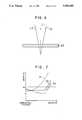
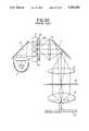
- FIG. 20shows a conventional projection aligner.
- a fly-eye lens 3is disposed diagonally to a lamp house 1.
- a mirror 2is disposed between the lens 3 and the house 1.
- An aperture member 4is positioned in front of the fly-eye lens 3.
- Condenser lenses 5 and 6, a mirror 7, and an exposure mask 8 on which a desired circuit pattern is formedare arranged along an optical path.
- a wafer 10is situated in front of the mask 8, and a projecting lens system 9 is disposed between the mask 8 and the wafer 10.
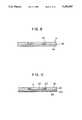
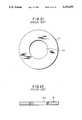
- the aperture member 4has a disk-like configuration with a circular opening 4a at the center thereof.
- Light emanating from the lamp house 1reaches the fly-eye lens 3 through the mirror 2, and is split into light beams which pass through lenses 3a, of the fly-eye lens 3.
- the light transmitted through the respective lenses 3apass through the opening 4a of the aperture member 4, the condenser lens 5, the mirror 7 and the condenser lens 6, and then irradiate an exposure zone of the mask 8.
- the light beams transmitted through the lenses 3a of the fly-eye lens 3are superposed on each other on the surface of the mask 8, and thus the beams irradiate uniformly the surface of the mask 8. In this way, the light beams pass through the mask 8 and reach the wafer 10 through the projecting lens system 9, whereby the circuit pattern is imaged on the surface of the wafer 10.
- the minimum resolution R of such a projection aligneris proportional to ⁇ /NA, where ⁇ is the wavelength being used and NA is the numerical aperture of the optical system.
- the optical systemhas hitherto been designed so that the numerical aperture is increased to improve the resolution of the projection aligner.
- the improved resolutioncopes with a higher degree of integration of LSIs.
- the object of the inventionis to provide a projection aligner increasing resolution and enlarging the depth of focus.
- a projection alignercomprising: a light source; a condenser lens system for directing light from the light source onto a mask on which a circuit pattern is formed; a projection lens system for collecting on the surface of a wafer the light transmitted through the mask; and an aperture member disposed between the light source and the condenser lens system wherein the aperture member includes a transmitting zone for transmitting the light emanating from the light source and a phase shift member for producing a predetermined phase shift between light transmitted through the center of the transmitting zone and light transmitted through a region surrounding the transmitting zone.
- FIG. 1is a view showing the optical system of a projection aligner in accordance with a first embodiment of the present invention
- FIG. 2is a plan view showing an aperture member used in the first embodiment
- FIG. 3is a cross-sectional view of the aperture member shown in FIG. 2;
- FIG. 4is a view showing the distribution of the intensity of light on the surface of a wafer when the light is completely focused thereon;
- FIG. 5is a view showing the distribution of the intensity of light on the surface of the wafer when the light is not focused thereon;
- FIG. 6is an enlarged view showing the surface of the wafer when the light is not focused thereon;
- FIG. 7is a view showing the result in which an optical image on the surface of the wafer is simulated when the width of a phase shift member of the aperture member is changed;
- FIG. 8is a cross-sectional view showing an aperture member used in a second embodiment
- FIG. 9is a plan view showing an aperture member used in a third embodiment.
- FIG. 10is a cross-sectional view of the aperture member shown in FIG. 9;
- FIG. 11is a cross-sectional view showing an aperture member used in a fourth embodiment
- FIG. 12is a view showing the optical system of a projection aligner in accordance with a fifth embodiment of the present invention.
- FIG. 13is a plan view showing an aperture member used in the fifth embodiment
- FIG. 14is a cross-sectional view of the aperture member shown in FIG. 13;
- FIG. 15is a view showing the distribution of the intensity of light on the surface of the wafer when the light is not focused thereon according to the fifth embodiment
- FIG. 16is a cross-sectional view of an aperture member used in a sixth embodiment
- FIG. 17is a plan view showing an aperture member used in a seventh embodiment
- FIG. 18is a cross-sectional view of the aperture member shown in FIG. 17;
- FIG. 19is a cross-sectional view showing an aperture member used in an eighth embodiment.
- FIG. 20is a view showing the optical system of the conventional projection aligner
- FIG. 21is a plan view of an aperture member used in the aligner shown in FIG. 20.
- FIG. 22is a cross-sectional view of the aperture member shown in FIG. 21.
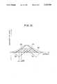
- FIG. 1is a view showing the optical system of a projection aligner in accordance with a first embodiment of the invention.
- a fly-eye lens 13is disposed diagonally to a lamp house 11 from a lamp which emits light having a wavelength of ⁇ , and a mirror 12 is disposed between the lens 13 and the house 11.
- An aperture member 21is positioned in front of the fly-eye lens 13.
- Condenser lenses 15 and 16, a mirror 17, and an exposure mask 18 on which a desired circuit pattern is formedare arranged along an optical path.
- a wafer 20is situated in front of the mask 18, and a projecting lens system 19 is disposed between the mask 18 and the wafer 20.
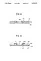
- the aperture member 21has a disk-like outer frame 22 and an annular phase shift member 23 having a width W.
- a circular opening 22a having a radius Ais formed at the center of the frame 22.
- the phase shift member 23is formed around the periphery of the opening 22a.
- the outer frame 22is formed of a light-intercepting, i.e., opaque member such as metal.
- the opening 22aforms a transmitting zone D through which light from the lamp house 11 is transmitted.
- the phase shift member 23is formed of, for example, SiO 2 , and is also formed to such a thickness that there is a phase difference of a half-wavelength, ⁇ /2, between light transmitted through the center of the transmitting zone D, where there is no phase shift member 23 present, and light transmitted through the phase shift member 23.
- the phases of light beams L2 and L3 transmitted through the phase shift member 23 of the aperture member 21are reversed with respect to the phase of light beam L1 transmitted through the center of the transmitting zone D. Therefore, when these light beams L1-L3 collect on the surface of the wafer 20, the light beams L2 and L3, each in a reverse phase, interfere with the light beam L1, thus offsetting each other.
- FIG. 4is a view showing the distribution of the intensity of light on the surface of the wafer when the light beams are completely focused thereon. If the aperture member 21 were not provided with the phase shift member 23, the distribution would be formed as indicated by a broken line 25. In this embodiment, however, because the aperture member 21 is provided with the phase shift member 23, the light beam L1 is offset by a reverse component 26 of the light beams L2 and L3, and thus the distribution of the intensity of light is formed as indicated by a solid line 24. It is thus proved that when the lights are completely focused, because of the provision of the phase shift member 23, there is a decrease in the intensity of light, but there is substantially no deterioration in the shape of the distribution of the intensity of light.
- the light beams L1-L3do not converge at one point on the surface of the wafer 20.
- the reverse components of light beams L2 and L3, transmitted through the phase shift member 23are distributed only around the center of a portion where the light beam L1 is most intense. For this reason, only the intensity of light around a distribution line formed when the aperture member 21 is not provided with the phase shift member 23 is offset by reverse components 29 and 30 of the light beams L2 and L3. In reality, the intensity of light is distributed as indicated by a solid line 27.
- the projection aligner shown in FIG. 1permits enlargement of the DOF, as described above, while at the same time increasing the numerical aperture NA.
- FIG. 7shows the results of the simulation.
- the abscissa of FIG. 7indicates the degree of focus, the amount of defocus increasing toward the right.
- the ordinateindicates the width of a 25% distribution of the maximum intensity Ip, that is, one-fourth of the Ip of the optical image, as shown in FIG. 4.
- Symbol B 0 in FIG. 7indicates an example of an allowable value of the width of the optical image when the circuit pattern is transferred.
- An optical image having a width B not greater than the allowable value B 0is required for accurate transferral.
- the phase difference between light transmitted through the center of the transmitting zone D and light transmitted through a portion around the transmitting zone D, due to the phase shift member 23,is not limited to a half-wavelength.
- the use of the half-wavelengthis the most effective in enlarging the DOF.
- FIG. 8shows an aperture member 41 used in a second embodiment.
- the aperture member 41is constructed in such a way that an outer frame 42 and a phase shift member 43 are formed on a crystalline substrate 44.
- the deposition of SiO 2 on the crystal substrate 44permits easy formation of the phase shift member 43.
- FIGS. 9 and 10both show an aperture member 51 used in a third embodiment.
- the aperture member 51is constructed in such a manner that a circular phase shift member 53 is formed at the center of a circular opening 52a in an outer frame 52.
- the phase shift member 53is formed on a crystalline substrate 54.
- the phase of light transmitted through the center of a transmitting zone Dis reversed with respect to the phase of light transmitted through a portion around the zone D.
- the same advantage as that described with the aperture member 21is obtainable.
- FIG. 11shows an aperture member 61 used in a fourth embodiment.
- the aperture member 61is constructed in the following way. First, an outer flame 62 and a phase shift member 63 are formed on a crystalline substrate 64. Then, antireflection films 65 and 66 made of, for example, MgF 2 , are formed on the phase shift member 63 and the crystalline substrate 64 exposed outside. The formation of the antireflection films 65 and 66 reduces the amount of stray light, thus resulting in improved resolution and contrast of an image.
- the antireflection filmmay be formed on either the obverse or the reverse surface of a transmitting zone D. In FIG. 11, although the antireflection films are formed on the aperture member with the structure shown in FIG. 8, they may be provided on any of the aperture members with the structures described above. The same advantage as that described above is obtainable.
- FIG. 12is a view showing the optical system of a projection aligner in accordance with a fifth embodiment of this invention.
- an aperture member 71is used in place of the aperture member 21 of the optical system in the first embodiment shown in FIG. 1.
- the aperture member 71has a circular outer frame 72, an annular phase shift member 73, and an annular light-intercepting member 74.
- a circular opening 72a having a radius Ais disposed at the center of the outer frame 72.
- the phase shift member 73 having a width W 1is disposed around the periphery of the opening 72a.
- the light-intercepting member 74 having a width W 2is formed around the inside periphery of the phase shift member 73.
- the center of a transmitting zone Dis separated by the light-intercepting member 74 from a portion around the zone D.
- the outer frame 72 and the light-intercepting member 74are made of an opaque material, such as metal, which blocks light.
- the phase shift member 73is made of, for instance, SiO 2 .
- the ratio W 2 /A of the width W 2 of the light-intercepting member 74 to the radius A of the transmitting zone D of the aperture member 71was changed and a circular contact hole pattern-exposed. It was found that when the ratio W 2 /A is about 3%, the circuit pattern can be most stably transferred.
- an aperture member 81constructed in such a way that an outer frame 82, a phase shift member 83, and a light-intercepting member 84 are formed on one crystalline substrate 85.
- the deposition of SiO 2 and metal on the crystalline substrate 85permits easy formation of the phase shift member 83 and the light-intercepting member 84.
- a circular phase shift member 93may be formed at the center of a circular opening 92a in an outer frame 92 and a light-intercepting member 94 may be formed around the phase shift member 93.
- the phase shift member 93 and the light-intercepting member 94are formed on a crystalline substrate 95.
- the formation of antireflection films 106 and 107 made of, for example, MgF 2reduces the amount of stray light, thus resulting in improved resolution and contrast of an image.
- an outer frame 102, a phase shift member 103, and a light-intercepting member 104are formed on a crystalline substrate 105.
- the antireflection film 106is formed on the phase shift member 103, the light-intercepting member 104 and the obverse side of the crystalline substrate 105, and the antireflection film 107 is formed on the reverse side of the crystalline substrate 105.
- the antireflection filmmay be formed on either the obverse or the reverse surface of a transmitting zone D.
- the antireflection filmsare formed on the aperture member with the structure shown in FIG. 16, they may be provided on an aperture member with a different structure. The same advantage as that described above is obtainable.
Landscapes
- Physics & Mathematics (AREA)
- General Physics & Mathematics (AREA)
- Exposure And Positioning Against Photoresist Photosensitive Materials (AREA)
Abstract
Description
1. Field of the Invention
The present invention relates to a projection aligner for use in the process of manufacturing LSIs.
2. Description of the Related Art
FIG. 20 shows a conventional projection aligner. A fly-eye lens 3 is disposed diagonally to a lamp house 1. Amirror 2 is disposed between thelens 3 and the house 1. Anaperture member 4 is positioned in front of the fly-eye lens 3.Condenser lenses 5 and 6, amirror 7, and anexposure mask 8 on which a desired circuit pattern is formed are arranged along an optical path. Awafer 10 is situated in front of themask 8, and a projecting lens system 9 is disposed between themask 8 and thewafer 10.
As shown in FIGS. 21 and 22, theaperture member 4 has a disk-like configuration with acircular opening 4a at the center thereof.
Light emanating from the lamp house 1 reaches the fly-eye lens 3 through themirror 2, and is split into light beams which pass throughlenses 3a, of the fly-eye lens 3. The light transmitted through therespective lenses 3a pass through the opening 4a of theaperture member 4, thecondenser lens 5, themirror 7 and the condenser lens 6, and then irradiate an exposure zone of themask 8. The light beams transmitted through thelenses 3a of the fly-eye lens 3 are superposed on each other on the surface of themask 8, and thus the beams irradiate uniformly the surface of themask 8. In this way, the light beams pass through themask 8 and reach thewafer 10 through the projecting lens system 9, whereby the circuit pattern is imaged on the surface of thewafer 10.
It is known that the minimum resolution R of such a projection aligner is proportional to λ/NA, where λ is the wavelength being used and NA is the numerical aperture of the optical system. Thus, the optical system has hitherto been designed so that the numerical aperture is increased to improve the resolution of the projection aligner. In recent years the improved resolution copes with a higher degree of integration of LSIs.
It is also known that as the numerical aperture of an optical system increases, the minimum resolution R decreases and the depth of focus (DOF) of the projection aligner also decreases even more than the resolution R does. The DOF is proportional to λ/NA2. For this reason, in the conventional projection aligner, the DOF decreases with an increase in the resolution, and the accuracy in transferring transcribing the circuit pattern deteriorates.
The present invention has been made to solve such a problem. Accordingly, the object of the invention is to provide a projection aligner increasing resolution and enlarging the depth of focus.
In order to achieve the above object, according to this invention, there is provided a projection aligner comprising: a light source; a condenser lens system for directing light from the light source onto a mask on which a circuit pattern is formed; a projection lens system for collecting on the surface of a wafer the light transmitted through the mask; and an aperture member disposed between the light source and the condenser lens system wherein the aperture member includes a transmitting zone for transmitting the light emanating from the light source and a phase shift member for producing a predetermined phase shift between light transmitted through the center of the transmitting zone and light transmitted through a region surrounding the transmitting zone.
FIG. 1 is a view showing the optical system of a projection aligner in accordance with a first embodiment of the present invention;
FIG. 2 is a plan view showing an aperture member used in the first embodiment;
FIG. 3 is a cross-sectional view of the aperture member shown in FIG. 2;
FIG. 4 is a view showing the distribution of the intensity of light on the surface of a wafer when the light is completely focused thereon;
FIG. 5 is a view showing the distribution of the intensity of light on the surface of the wafer when the light is not focused thereon;
FIG. 6 is an enlarged view showing the surface of the wafer when the light is not focused thereon;
FIG. 7 is a view showing the result in which an optical image on the surface of the wafer is simulated when the width of a phase shift member of the aperture member is changed;
FIG. 8 is a cross-sectional view showing an aperture member used in a second embodiment;
FIG. 9 is a plan view showing an aperture member used in a third embodiment;
FIG. 10 is a cross-sectional view of the aperture member shown in FIG. 9;
FIG. 11 is a cross-sectional view showing an aperture member used in a fourth embodiment;
FIG. 12 is a view showing the optical system of a projection aligner in accordance with a fifth embodiment of the present invention;
FIG. 13 is a plan view showing an aperture member used in the fifth embodiment;
FIG. 14 is a cross-sectional view of the aperture member shown in FIG. 13;
FIG. 15 is a view showing the distribution of the intensity of light on the surface of the wafer when the light is not focused thereon according to the fifth embodiment;
FIG. 16 is a cross-sectional view of an aperture member used in a sixth embodiment;
FIG. 17 is a plan view showing an aperture member used in a seventh embodiment;
FIG. 18 is a cross-sectional view of the aperture member shown in FIG. 17;
FIG. 19 is a cross-sectional view showing an aperture member used in an eighth embodiment;
FIG. 20 is a view showing the optical system of the conventional projection aligner;
FIG. 21 is a plan view of an aperture member used in the aligner shown in FIG. 20; and
FIG. 22 is a cross-sectional view of the aperture member shown in FIG. 21.
The embodiments of the present invention will be described below with reference to the accompanying drawings.
FIG. 1 is a view showing the optical system of a projection aligner in accordance with a first embodiment of the invention. A fly-eye lens 13 is disposed diagonally to alamp house 11 from a lamp which emits light having a wavelength of λ, and amirror 12 is disposed between thelens 13 and thehouse 11. Anaperture member 21 is positioned in front of the fly-eye lens 13.Condenser lenses 15 and 16, amirror 17, and anexposure mask 18 on which a desired circuit pattern is formed are arranged along an optical path. Awafer 20 is situated in front of themask 18, and aprojecting lens system 19 is disposed between themask 18 and thewafer 20.
As shown in FIGS. 2 and 3, theaperture member 21 has a disk-likeouter frame 22 and an annularphase shift member 23 having a width W. Acircular opening 22a having a radius A is formed at the center of theframe 22. Thephase shift member 23 is formed around the periphery of the opening 22a. Theouter frame 22 is formed of a light-intercepting, i.e., opaque member such as metal. The opening 22a forms a transmitting zone D through which light from thelamp house 11 is transmitted. Thephase shift member 23 is formed of, for example, SiO2, and is also formed to such a thickness that there is a phase difference of a half-wavelength, λ/2, between light transmitted through the center of the transmitting zone D, where there is nophase shift member 23 present, and light transmitted through thephase shift member 23.
The operation of this embodiment will now be explained. Light from thelamp house 11 reaches the fly-eye lens 13 through themirror 12, and is split into light beams which pass throughlenses 13a, which constitute the fly-eye lens 13. The light beams transmitted through therespective lenses 13a pass through the transmitting zone D of theaperture member 21, the condenser lens 15, themirror 17 and thecondenser lens 16, and then irradiate an exposure zone of themask 18. The light beams transmitted through thelenses 13a of the fly-eye lens 13 are superposed on each other on the surface of themask 18, and thus the beams irradiate uniformly the surface of themask 18. In this way, the light beams pass through themask 18 and reach thewafer 20 through the projectinglens system 19, whereby an image of the circuit pattern is formed on the surface of thewafer 20.
As shown in FIG. 1, because of thephase shift member 23 formed at the periphery of the transmitting zone D of theaperture member 21, the phases of light beams L2 and L3 transmitted through thephase shift member 23 of theaperture member 21 are reversed with respect to the phase of light beam L1 transmitted through the center of the transmitting zone D. Therefore, when these light beams L1-L3 collect on the surface of thewafer 20, the light beams L2 and L3, each in a reverse phase, interfere with the light beam L1, thus offsetting each other.
FIG. 4 is a view showing the distribution of the intensity of light on the surface of the wafer when the light beams are completely focused thereon. If theaperture member 21 were not provided with thephase shift member 23, the distribution would be formed as indicated by abroken line 25. In this embodiment, however, because theaperture member 21 is provided with thephase shift member 23, the light beam L1 is offset by areverse component 26 of the light beams L2 and L3, and thus the distribution of the intensity of light is formed as indicated by asolid line 24. It is thus proved that when the lights are completely focused, because of the provision of thephase shift member 23, there is a decrease in the intensity of light, but there is substantially no deterioration in the shape of the distribution of the intensity of light.
On the other hand, when the light are beams not focused on thewafer 20 as shown in FIG. 6, the light beams L1-L3 do not converge at one point on the surface of thewafer 20. Thus, as indicated by dot chain lines of FIG. 5, the reverse components of light beams L2 and L3, transmitted through thephase shift member 23, are distributed only around the center of a portion where the light beam L1 is most intense. For this reason, only the intensity of light around a distribution line formed when theaperture member 21 is not provided with thephase shift member 23 is offset byreverse components solid line 27. For this reason, when the light beams are defocused, that is, when the light beams L1-L3 do not converge at one point on the surface of thewafer 20, only the intensity of light around a defocused image decreases. Then the image contrast is improved, so that it approaches the level of image contrast when the light beams are focused. In other words, an image of sharp contrast is obtainable in a wide optical axis direction, and the depth of focus (DOF) is enlarged.
The projection aligner shown in FIG. 1 permits enlargement of the DOF, as described above, while at the same time increasing the numerical aperture NA.
The ratio of the width W of thephase shift member 23 to the radius A of the transmitting zone D of theaperture member 21 is changed and an optical image contrast on the surface of thewafer 20 is simulated. FIG. 7 shows the results of the simulation. The abscissa of FIG. 7 indicates the degree of focus, the amount of defocus increasing toward the right. The ordinate indicates the width of a 25% distribution of the maximum intensity Ip, that is, one-fourth of the Ip of the optical image, as shown in FIG. 4. Symbol B0 in FIG. 7 indicates an example of an allowable value of the width of the optical image when the circuit pattern is transferred. An optical image having a width B not greater than the allowable value B0 is required for accurate transferral.
In the case of W/A=0, that is, when thephase shift member 23 is not provided, as indicated by abroken line 31, the width B of the optical image increases sharply with an increase in the degree of defocusing, whereas the contrast decreases. In the case of W/A=5%, as indicated by asolid line 32, even when there is some increase in the degree of defocusing, the optical image exhibits a constant value which is substantially equal to the width B when the light beams are completely focused. The value the increase, exceeding the allowable value B0. In the case of W/A=10%, as indicated by adot chain line 33, as the degree of defocus increases, the width B of the optical image first decreases, and then increases and exceeds the allowable value B0. The results of such a simulation prove that the use of theaperture member 21 satisfying a relationship W/A=5% is effective in accurately and stably transferring the circuit pattern.
The phase difference between light transmitted through the center of the transmitting zone D and light transmitted through a portion around the transmitting zone D, due to thephase shift member 23, is not limited to a half-wavelength. However, as described in the embodiment mentioned above, the use of the half-wavelength is the most effective in enlarging the DOF.
FIG. 8 shows anaperture member 41 used in a second embodiment. Theaperture member 41 is constructed in such a way that anouter frame 42 and aphase shift member 43 are formed on acrystalline substrate 44. In this embodiment, the deposition of SiO2 on thecrystal substrate 44 permits easy formation of thephase shift member 43.
FIGS. 9 and 10 both show anaperture member 51 used in a third embodiment. Theaperture member 51 is constructed in such a manner that a circularphase shift member 53 is formed at the center of acircular opening 52a in anouter frame 52. Thephase shift member 53 is formed on acrystalline substrate 54. In theaperture member 51, as opposed to theaperture member 21 shown in FIGS. 2 and 3, the phase of light transmitted through the center of a transmitting zone D is reversed with respect to the phase of light transmitted through a portion around the zone D. The same advantage as that described with theaperture member 21 is obtainable.
FIG. 11 shows anaperture member 61 used in a fourth embodiment. Theaperture member 61 is constructed in the following way. First, anouter flame 62 and aphase shift member 63 are formed on acrystalline substrate 64. Then,antireflection films phase shift member 63 and thecrystalline substrate 64 exposed outside. The formation of theantireflection films
FIG. 12 is a view showing the optical system of a projection aligner in accordance with a fifth embodiment of this invention. In this embodiment, anaperture member 71 is used in place of theaperture member 21 of the optical system in the first embodiment shown in FIG. 1. As illustrated in FIGS. 13 and 14, theaperture member 71 has a circularouter frame 72, an annularphase shift member 73, and an annular light-interceptingmember 74. Acircular opening 72a having a radius A is disposed at the center of theouter frame 72. Thephase shift member 73 having a width W1 is disposed around the periphery of theopening 72a. The light-interceptingmember 74 having a width W2 is formed around the inside periphery of thephase shift member 73. In other words, the center of a transmitting zone D is separated by the light-interceptingmember 74 from a portion around the zone D. Theouter frame 72 and the light-interceptingmember 74 are made of an opaque material, such as metal, which blocks light. Thephase shift member 73 is made of, for instance, SiO2.
When theaperture member 71 having a such a light-interceptingmember 74 is used, as indicated by dot chain lines of FIG. 15, when the lights are defocused, the centers ofreverse components phase shift member 73, will deviate in an amount equal to a predetermined distance W3 fromcomponents 38 of a light beam L1 which are positioned most outwardly. For this reason, only light in a portion around a distribution line formed when theaperture member 71 is not provided with thephase shift member 73 is offset by thereverse components solid line 34. Thus, when the light beams are defocused, only the intensity of light around a defocused image decreases, and the image contrast is considerably improved, so that it approaches the level of image contrast when the light beams are completely focused. In other words, an image of sharp contrast is obtainable in a wide optical axis direction, and the depth of focus (DOF) is enlarged.
The ratio W2 /A of the width W2 of the light-interceptingmember 74 to the radius A of the transmitting zone D of theaperture member 71 was changed and a circular contact hole pattern-exposed. It was found that when the ratio W2 /A is about 3%, the circuit pattern can be most stably transferred.
As shown in FIG. 16, it may also be possible to employ anaperture member 81 constructed in such a way that anouter frame 82, aphase shift member 83, and a light-interceptingmember 84 are formed on onecrystalline substrate 85. In such a case, the deposition of SiO2 and metal on thecrystalline substrate 85 permits easy formation of thephase shift member 83 and the light-interceptingmember 84.
Alternatively, as in anaperture member 91 shown in FIGS. 17 and 18, a circularphase shift member 93 may be formed at the center of acircular opening 92a in anouter frame 92 and a light-interceptingmember 94 may be formed around thephase shift member 93. Thephase shift member 93 and the light-interceptingmember 94 are formed on acrystalline substrate 95.
As in anaperture member 101 depicted in FIG. 19, the formation ofantireflection films aperture member 101, first, anouter frame 102, aphase shift member 103, and a light-interceptingmember 104 are formed on acrystalline substrate 105. Then, theantireflection film 106 is formed on thephase shift member 103, the light-interceptingmember 104 and the obverse side of thecrystalline substrate 105, and theantireflection film 107 is formed on the reverse side of thecrystalline substrate 105. The antireflection film may be formed on either the obverse or the reverse surface of a transmitting zone D. In FIG. 19, although the antireflection films are formed on the aperture member with the structure shown in FIG. 16, they may be provided on an aperture member with a different structure. The same advantage as that described above is obtainable.
Claims (14)
1. A projection aligner comprising:
a light source for producing light;
a condenser lens system for directing light from said light source onto a mask on which a circuit pattern is formed;
a projecting lens system for collecting on the surface of a wafer the light transmitted through said mask; and
an aperture member disposed between said light source and said condenser lens system wherein said aperture member includes a transmitting zone for transmitting light from said light source and a phase shift member for producing a predetermined phase difference between light transmitted through the transmitting zone and light transmitted through a region surrounding the transmitting zone.
2. A projection aligner as claimed in claim 1 wherein said phase shift member is an annular member defining a periphery of the transmitting zone of said aperture member.
3. A projection aligner as claimed in claim 1 wherein said phase shift member produces a phase difference of one half-wavelength.
4. A projection aligner as claimed in claim 1 wherein said phase shift member is SiO2.
5. A projection aligner as claimed in claim 1 wherein said aperture member includes an annular light-intercepting member separating the transmitting zone from the region surrounding the transmitting zone.
6. A projection aligner as claimed in claim 5 wherein the transmitting zone is circular and has a radius A, said light-intercepting member is annular, has width W2, and is concentric with the transmitting zone, and the ratio W2 /A is substantially 3%.
7. A projection aligner as claimed in claim 5 wherein said light-intercepting member is metal.
8. A projection aligner as claimed in claim 1 wherein said aperture member includes a transparent substrate, an outer frame disposed on said transparent substrate and having a central opening defining the transmitting zone, and said phase shift member is disposed on the transparent substrate within the opening of said outer frame.
9. A projection aligner as claimed in claim 8 wherein said transparent substrate is quartz, and said outer frame is metal.
10. A projection aligner as claimed in claim 1 wherein said aperture member includes an antireflection film within the transmitting zone.
11. A projection aligner as claimed in claim 10 wherein said antireflection film is MgF2.
12. A projection aligner as claimed in claim 1 wherein the transmitting zone is circular and has a radius A, said phase shift member is annular and has width W1, and the ratio W1 /A is substantially 5%.
13. A projection aligner comprising:
a light source for producing light;
a condenser lens system for directing light from said light source onto a mask on which a circuit pattern is formed;
a projecting lens system for collecting on the surface of a wafer the light transmitted through said mask; and
an aperture member disposed between said light source and said condenser lens system wherein said aperture member includes a transmitting zone for transmitting light from said light source and a phase shift member within the transmitting zone for producing a predetermined phase difference between light transmitted only through the transmitting zone and light transmitted through the transmitting zone and the phase shift member.
14. A projection aligner as claimed in claim 13 wherein said phase shift member is a disc-like member centrally disposed within the transmitting zone of said aperture member with an annular region of the transmitting zone surrounding said phase shift member.
Applications Claiming Priority (4)
| Application Number | Priority Date | Filing Date | Title |
|---|---|---|---|
| JP2302780AJP2587132B2 (en) | 1990-11-09 | 1990-11-09 | Projection exposure equipment |
| JP2-302780 | 1990-11-09 | ||
| JP3-11540 | 1991-01-08 | ||
| JP3011540AJP2581845B2 (en) | 1991-01-08 | 1991-01-08 | Projection exposure equipment |
Publications (1)
| Publication Number | Publication Date |
|---|---|
| US5253040Atrue US5253040A (en) | 1993-10-12 |
Family
ID=26346979
Family Applications (1)
| Application Number | Title | Priority Date | Filing Date |
|---|---|---|---|
| US07/788,235Expired - LifetimeUS5253040A (en) | 1990-11-09 | 1991-11-05 | Projection aligner |
Country Status (1)
| Country | Link |
|---|---|
| US (1) | US5253040A (en) |
Cited By (22)
| Publication number | Priority date | Publication date | Assignee | Title |
|---|---|---|---|---|
| US5311249A (en)* | 1992-02-13 | 1994-05-10 | Mitsubishi Denki Kabushiki Kaisha | Projection exposure apparatus |
| US5323208A (en)* | 1992-03-09 | 1994-06-21 | Hitachi, Ltd. | Projection exposure apparatus |
| US5329335A (en)* | 1992-03-17 | 1994-07-12 | Nippon Steel Corporation | Method and apparatus for projection exposure |
| US5331369A (en)* | 1991-09-20 | 1994-07-19 | Hitachi, Ltd. | Method of forming patterns and apparatus for carrying out the same |
| EP0607674A1 (en)* | 1992-12-31 | 1994-07-27 | AT&T Corp. | Optical lithographical imaging system including optical transmission diffraction devices |
| US5335044A (en)* | 1992-02-26 | 1994-08-02 | Nikon Corporation | Projection type exposure apparatus and method of exposure |
| US5367358A (en)* | 1992-10-09 | 1994-11-22 | Mitsubishi Denki Kabushiki Kaisha | Projection exposing apparatus and projection exposing method |
| US5396311A (en)* | 1992-09-18 | 1995-03-07 | Sharp Kabushiki Kaisha | Filter for projection photolithographic system |
| US5424803A (en)* | 1991-08-09 | 1995-06-13 | Canon Kabushiki Kaisha | Projection exposure apparatus and semiconductor device manufacturing method |
| US5432588A (en)* | 1993-02-08 | 1995-07-11 | Mitsubishi Denk Kabushiki Kaisha | Semiconductor device and method of making the semiconductor device |
| US5530518A (en)* | 1991-12-25 | 1996-06-25 | Nikon Corporation | Projection exposure apparatus |
| DE19606170A1 (en)* | 1995-02-20 | 1996-08-22 | Sharp Kk | Light source filter for projecting masking images on to semiconductor wafers for lithographic micro-miniaturisation process |
| US5552856A (en)* | 1993-06-14 | 1996-09-03 | Nikon Corporation | Projection exposure apparatus |
| US5631773A (en)* | 1991-08-02 | 1997-05-20 | Canon Kabushiki Kaisha | Image projection method and semiconductor device manufacturing method using the same |
| US5673102A (en)* | 1991-02-22 | 1997-09-30 | Canon Kabushiki Kaisha | Image farming and microdevice manufacturing method and exposure apparatus in which a light source includes four quadrants of predetermined intensity |
| US6108089A (en)* | 1995-10-11 | 2000-08-22 | Nikon Corporation | Position detecting apparatus and method for projection exposure apparatus |
| US6271909B1 (en)* | 1991-02-22 | 2001-08-07 | Canon Kabushiki Kaisha | Exposure apparatus and device manufacturing method including changing a photo-intensity distribution of a light source and adjusting an illuminance distribution on a substrate in accordance with the change |
| US20060078805A1 (en)* | 2004-10-12 | 2006-04-13 | Asml Netherlands B.V. | Lithographic apparatus and device manufacturing method |
| USRE39662E1 (en)* | 1991-12-25 | 2007-05-29 | Nikon Corporation | Projection exposure apparatus |
| WO2008074998A1 (en)* | 2006-12-18 | 2008-06-26 | Renishaw Plc | Phase constrast encoding |
| US20090311636A1 (en)* | 2008-06-16 | 2009-12-17 | Canon Kabushiki Kaisha | Exposure apparatus, device manufacturing method, and aperture stop manufacturing method |
| US20150036116A1 (en)* | 2013-08-02 | 2015-02-05 | United Microelectronics Corp. | Aperture for photolithography |
Citations (6)
| Publication number | Priority date | Publication date | Assignee | Title |
|---|---|---|---|---|
| US3157087A (en)* | 1961-12-26 | 1964-11-17 | Pako Corp | Optical light distribution system for a photographic projection printer |
| US3892482A (en)* | 1974-03-07 | 1975-07-01 | Berkey Photo Inc | Color correcting illumination system for color enlargers and the like |
| US4257086A (en)* | 1979-10-22 | 1981-03-17 | Koehler Manufacturing Company | Method and apparatus for controlling radiant energy |
| US4816876A (en)* | 1985-11-27 | 1989-03-28 | Pryor Paul L | Contrast control for lens |
| US4970546A (en)* | 1988-04-07 | 1990-11-13 | Nikon Corporation | Exposure control device |
| US4988188A (en)* | 1987-08-31 | 1991-01-29 | Canon Kabushiki Kaisha | Illumination device |
- 1991
- 1991-11-05USUS07/788,235patent/US5253040A/ennot_activeExpired - Lifetime
Patent Citations (6)
| Publication number | Priority date | Publication date | Assignee | Title |
|---|---|---|---|---|
| US3157087A (en)* | 1961-12-26 | 1964-11-17 | Pako Corp | Optical light distribution system for a photographic projection printer |
| US3892482A (en)* | 1974-03-07 | 1975-07-01 | Berkey Photo Inc | Color correcting illumination system for color enlargers and the like |
| US4257086A (en)* | 1979-10-22 | 1981-03-17 | Koehler Manufacturing Company | Method and apparatus for controlling radiant energy |
| US4816876A (en)* | 1985-11-27 | 1989-03-28 | Pryor Paul L | Contrast control for lens |
| US4988188A (en)* | 1987-08-31 | 1991-01-29 | Canon Kabushiki Kaisha | Illumination device |
| US4970546A (en)* | 1988-04-07 | 1990-11-13 | Nikon Corporation | Exposure control device |
Cited By (32)
| Publication number | Priority date | Publication date | Assignee | Title |
|---|---|---|---|---|
| US20040080736A1 (en)* | 1991-02-22 | 2004-04-29 | Canon Kabushiki Kaisha | Imaging method for manufacture of microdevices |
| US6654101B2 (en) | 1991-02-22 | 2003-11-25 | Canon Kabushiki Kaisha | Exposure apparatus and device manufacturing method including changing a photo-intensity distribution of a light source and adjusting an illuminance distribution on a substrate in accordance with the change |
| US6473160B2 (en) | 1991-02-22 | 2002-10-29 | Canon Kabushiki Kaisha | Projection exposure apparatus and device manufacturing method including an aperture member having a circular light transmitting portion and a light blocking member |
| US6271909B1 (en)* | 1991-02-22 | 2001-08-07 | Canon Kabushiki Kaisha | Exposure apparatus and device manufacturing method including changing a photo-intensity distribution of a light source and adjusting an illuminance distribution on a substrate in accordance with the change |
| US6128068A (en)* | 1991-02-22 | 2000-10-03 | Canon Kabushiki Kaisha | Projection exposure apparatus including an illumination optical system that forms a secondary light source with a particular intensity distribution |
| US6084655A (en)* | 1991-02-22 | 2000-07-04 | Canon Kabushiki Kaisha | Imaging method for manufacture of microdevices |
| US5673102A (en)* | 1991-02-22 | 1997-09-30 | Canon Kabushiki Kaisha | Image farming and microdevice manufacturing method and exposure apparatus in which a light source includes four quadrants of predetermined intensity |
| US5631773A (en)* | 1991-08-02 | 1997-05-20 | Canon Kabushiki Kaisha | Image projection method and semiconductor device manufacturing method using the same |
| US5424803A (en)* | 1991-08-09 | 1995-06-13 | Canon Kabushiki Kaisha | Projection exposure apparatus and semiconductor device manufacturing method |
| US5331369A (en)* | 1991-09-20 | 1994-07-19 | Hitachi, Ltd. | Method of forming patterns and apparatus for carrying out the same |
| USRE39662E1 (en)* | 1991-12-25 | 2007-05-29 | Nikon Corporation | Projection exposure apparatus |
| US5530518A (en)* | 1991-12-25 | 1996-06-25 | Nikon Corporation | Projection exposure apparatus |
| US5311249A (en)* | 1992-02-13 | 1994-05-10 | Mitsubishi Denki Kabushiki Kaisha | Projection exposure apparatus |
| US5335044A (en)* | 1992-02-26 | 1994-08-02 | Nikon Corporation | Projection type exposure apparatus and method of exposure |
| US5323208A (en)* | 1992-03-09 | 1994-06-21 | Hitachi, Ltd. | Projection exposure apparatus |
| US5329335A (en)* | 1992-03-17 | 1994-07-12 | Nippon Steel Corporation | Method and apparatus for projection exposure |
| US5396311A (en)* | 1992-09-18 | 1995-03-07 | Sharp Kabushiki Kaisha | Filter for projection photolithographic system |
| US5367358A (en)* | 1992-10-09 | 1994-11-22 | Mitsubishi Denki Kabushiki Kaisha | Projection exposing apparatus and projection exposing method |
| EP0607674A1 (en)* | 1992-12-31 | 1994-07-27 | AT&T Corp. | Optical lithographical imaging system including optical transmission diffraction devices |
| US5432588A (en)* | 1993-02-08 | 1995-07-11 | Mitsubishi Denk Kabushiki Kaisha | Semiconductor device and method of making the semiconductor device |
| US5552856A (en)* | 1993-06-14 | 1996-09-03 | Nikon Corporation | Projection exposure apparatus |
| DE19606170A1 (en)* | 1995-02-20 | 1996-08-22 | Sharp Kk | Light source filter for projecting masking images on to semiconductor wafers for lithographic micro-miniaturisation process |
| US6108089A (en)* | 1995-10-11 | 2000-08-22 | Nikon Corporation | Position detecting apparatus and method for projection exposure apparatus |
| EP1647862A1 (en)* | 2004-10-12 | 2006-04-19 | ASML Netherlands B.V. | Lithographic apparatus and device manufacturing method |
| US20060078805A1 (en)* | 2004-10-12 | 2006-04-13 | Asml Netherlands B.V. | Lithographic apparatus and device manufacturing method |
| US7372540B2 (en) | 2004-10-12 | 2008-05-13 | Asml Netherlands B.V. | Lithographic apparatus and device manufacturing method |
| US20080180649A1 (en)* | 2004-10-12 | 2008-07-31 | Asml Netherlands B.V. | Lithographic apparatus and device manufacturing method |
| US7898644B2 (en) | 2004-10-12 | 2011-03-01 | Asml Netherlands B.V. | Lithographic apparatus and device manufacturing method |
| WO2008074998A1 (en)* | 2006-12-18 | 2008-06-26 | Renishaw Plc | Phase constrast encoding |
| US20090311636A1 (en)* | 2008-06-16 | 2009-12-17 | Canon Kabushiki Kaisha | Exposure apparatus, device manufacturing method, and aperture stop manufacturing method |
| US8305560B2 (en)* | 2008-06-16 | 2012-11-06 | Canon Kabushiki Kaisha | Exposure apparatus, device manufacturing method, and aperture stop manufacturing method |
| US20150036116A1 (en)* | 2013-08-02 | 2015-02-05 | United Microelectronics Corp. | Aperture for photolithography |
Similar Documents
| Publication | Publication Date | Title |
|---|---|---|
| US5144362A (en) | Projection aligner | |
| US5253040A (en) | Projection aligner | |
| US5264898A (en) | Projection exposure apparatus | |
| US5499137A (en) | Exposure method and apparatus therefor | |
| KR100306953B1 (en) | Projection Exposure Equipment and Methods | |
| US6004699A (en) | Photomask used for projection exposure with phase shifted auxiliary pattern | |
| US7629087B2 (en) | Photomask, method of making a photomask and photolithography method and system using the same | |
| JP2725895B2 (en) | Exposure mechanism | |
| US6057970A (en) | Apparatus for enhancing depth of focus using birefringent material | |
| JP3287017B2 (en) | Measurement method of imaging characteristics | |
| US5393623A (en) | Exposure apparatus employing a photomask | |
| US5311249A (en) | Projection exposure apparatus | |
| JPH06163350A (en) | Projection exposure method and device thereof | |
| JP3008744B2 (en) | Projection exposure apparatus and semiconductor device manufacturing method using the same | |
| US5384218A (en) | Photomask and pattern transfer method for transferring a pattern onto a substrate having different levels | |
| JP2972528B2 (en) | Exposure method | |
| JP2581845B2 (en) | Projection exposure equipment | |
| JP2908100B2 (en) | Projection exposure apparatus and method of manufacturing semiconductor device | |
| US5434647A (en) | Projector for exposing photosensitive substrate | |
| JP2587132B2 (en) | Projection exposure equipment | |
| JPH05315226A (en) | Projection aligner | |
| JP2581846B2 (en) | Projection exposure equipment | |
| JPH08250407A (en) | Manufacture of semiconductor device | |
| JPH0778753A (en) | Projection exposure apparatus and method of manufacturing semiconductor device using the same | |
| JP2587133B2 (en) | Projection exposure apparatus and semiconductor device exposed and manufactured by the apparatus |
Legal Events
| Date | Code | Title | Description |
|---|---|---|---|
| AS | Assignment | Owner name:MITSUBISHI DENKI KABUSHIKI KAISHA, JAPAN Free format text:ASSIGNMENT OF ASSIGNORS INTEREST.;ASSIGNORS:KAMON, KAZUYA;MYOI, YASUHITO;MIYAMOTO, TERUO;AND OTHERS;REEL/FRAME:005950/0741;SIGNING DATES FROM 19911107 TO 19911111 | |
| STCF | Information on status: patent grant | Free format text:PATENTED CASE | |
| FEPP | Fee payment procedure | Free format text:PAYOR NUMBER ASSIGNED (ORIGINAL EVENT CODE: ASPN); ENTITY STATUS OF PATENT OWNER: LARGE ENTITY | |
| FPAY | Fee payment | Year of fee payment:4 | |
| FPAY | Fee payment | Year of fee payment:8 | |
| FPAY | Fee payment | Year of fee payment:12 | |
| AS | Assignment | Owner name:RENESAS ELECTRONICS CORPORATION, JAPAN Free format text:ASSIGNMENT OF ASSIGNORS INTEREST;ASSIGNOR:MITSUBISHI DENKI KABUSHIKI KAISHA;REEL/FRAME:025980/0219 Effective date:20110307 |