US5252294A - Micromechanical structure - Google Patents
Micromechanical structureDownload PDFInfo
- Publication number
- US5252294A US5252294AUS07/830,755US83075592AUS5252294AUS 5252294 AUS5252294 AUS 5252294AUS 83075592 AUS83075592 AUS 83075592AUS 5252294 AUS5252294 AUS 5252294A
- Authority
- US
- United States
- Prior art keywords
- depressions
- lid
- micromechanical
- recited
- micromechanical structure
- Prior art date
- Legal status (The legal status is an assumption and is not a legal conclusion. Google has not performed a legal analysis and makes no representation as to the accuracy of the status listed.)
- Expired - Fee Related
Links
- 239000000126substanceSubstances0.000claimsabstractdescription39
- 238000011156evaluationMethods0.000claimsabstractdescription17
- 239000011521glassSubstances0.000claimsabstractdescription12
- OKTJSMMVPCPJKN-UHFFFAOYSA-NCarbonChemical compound[C]OKTJSMMVPCPJKN-UHFFFAOYSA-N0.000claimsabstractdescription4
- 229910052799carbonInorganic materials0.000claimsabstractdescription4
- 239000000919ceramicSubstances0.000claimsabstractdescription4
- 229910003460diamondInorganic materials0.000claimsabstractdescription4
- 239000010432diamondSubstances0.000claimsabstractdescription4
- 229910052710siliconInorganic materials0.000claimsdescription22
- 239000010703siliconSubstances0.000claimsdescription22
- 239000000463materialSubstances0.000claimsdescription17
- 238000012360testing methodMethods0.000claimsdescription14
- 238000011835investigationMethods0.000claimsdescription11
- 230000003287optical effectEffects0.000claimsdescription8
- 239000011159matrix materialSubstances0.000claimsdescription7
- 238000005259measurementMethods0.000claimsdescription4
- 238000009826distributionMethods0.000claimsdescription3
- 230000005693optoelectronicsEffects0.000claimsdescription3
- 238000007865dilutingMethods0.000claims1
- 239000013080microcrystalline materialSubstances0.000claims1
- 238000000034methodMethods0.000abstractdescription15
- 239000004065semiconductorSubstances0.000abstractdescription9
- 238000011160researchMethods0.000abstractdescription8
- 238000005516engineering processMethods0.000abstractdescription5
- 108090000623proteins and genesProteins0.000abstractdescription3
- 238000003486chemical etchingMethods0.000abstractdescription2
- 230000000873masking effectEffects0.000abstractdescription2
- 230000000737periodic effectEffects0.000abstractdescription2
- XUIMIQQOPSSXEZ-UHFFFAOYSA-NSiliconChemical compound[Si]XUIMIQQOPSSXEZ-UHFFFAOYSA-N0.000description22
- 210000004027cellAnatomy0.000description16
- 238000006243chemical reactionMethods0.000description16
- 239000007789gasSubstances0.000description14
- 239000000758substrateSubstances0.000description11
- 238000012986modificationMethods0.000description10
- 230000004048modificationEffects0.000description10
- 238000003860storageMethods0.000description10
- 238000001816coolingMethods0.000description9
- 238000011282treatmentMethods0.000description7
- 108090000790EnzymesProteins0.000description6
- 102000004190EnzymesHuman genes0.000description6
- 238000001444catalytic combustion detectionMethods0.000description6
- 238000013461designMethods0.000description6
- 239000007788liquidSubstances0.000description6
- 239000003153chemical reaction reagentSubstances0.000description5
- 230000015654memoryEffects0.000description5
- VYPSYNLAJGMNEJ-UHFFFAOYSA-NSilicium dioxideChemical compoundO=[Si]=OVYPSYNLAJGMNEJ-UHFFFAOYSA-N0.000description4
- 238000004458analytical methodMethods0.000description4
- 239000008280bloodSubstances0.000description4
- 210000004369bloodAnatomy0.000description4
- 239000013078crystalSubstances0.000description4
- 239000002178crystalline materialSubstances0.000description4
- 239000003814drugSubstances0.000description4
- 230000000694effectsEffects0.000description4
- 238000005530etchingMethods0.000description4
- 239000000969carrierSubstances0.000description3
- 230000008859changeEffects0.000description3
- 230000002596correlated effectEffects0.000description3
- 230000000875corresponding effectEffects0.000description3
- 230000005669field effectEffects0.000description3
- 239000011888foilSubstances0.000description3
- 238000010438heat treatmentMethods0.000description3
- 238000004519manufacturing processMethods0.000description3
- 239000013307optical fiberSubstances0.000description3
- 239000002245particleSubstances0.000description3
- 238000005192partitionMethods0.000description3
- IJGRMHOSHXDMSA-UHFFFAOYSA-NAtomic nitrogenChemical compoundN#NIJGRMHOSHXDMSA-UHFFFAOYSA-N0.000description2
- QVGXLLKOCUKJST-UHFFFAOYSA-Natomic oxygenChemical compound[O]QVGXLLKOCUKJST-UHFFFAOYSA-N0.000description2
- 238000010923batch productionMethods0.000description2
- 230000008901benefitEffects0.000description2
- 238000004159blood analysisMethods0.000description2
- 239000012876carrier materialSubstances0.000description2
- 230000003197catalytic effectEffects0.000description2
- HVYWMOMLDIMFJA-DPAQBDIFSA-NcholesterolChemical compoundC1C=C2C[C@@H](O)CC[C@]2(C)[C@@H]2[C@@H]1[C@@H]1CC[C@H]([C@H](C)CCCC(C)C)[C@@]1(C)CC2HVYWMOMLDIMFJA-DPAQBDIFSA-N0.000description2
- 238000010276constructionMethods0.000description2
- 239000000835fiberSubstances0.000description2
- 239000012530fluidSubstances0.000description2
- NOESYZHRGYRDHS-UHFFFAOYSA-NinsulinChemical compoundN1C(=O)C(NC(=O)C(CCC(N)=O)NC(=O)C(CCC(O)=O)NC(=O)C(C(C)C)NC(=O)C(NC(=O)CN)C(C)CC)CSSCC(C(NC(CO)C(=O)NC(CC(C)C)C(=O)NC(CC=2C=CC(O)=CC=2)C(=O)NC(CCC(N)=O)C(=O)NC(CC(C)C)C(=O)NC(CCC(O)=O)C(=O)NC(CC(N)=O)C(=O)NC(CC=2C=CC(O)=CC=2)C(=O)NC(CSSCC(NC(=O)C(C(C)C)NC(=O)C(CC(C)C)NC(=O)C(CC=2C=CC(O)=CC=2)NC(=O)C(CC(C)C)NC(=O)C(C)NC(=O)C(CCC(O)=O)NC(=O)C(C(C)C)NC(=O)C(CC(C)C)NC(=O)C(CC=2NC=NC=2)NC(=O)C(CO)NC(=O)CNC2=O)C(=O)NCC(=O)NC(CCC(O)=O)C(=O)NC(CCCNC(N)=N)C(=O)NCC(=O)NC(CC=3C=CC=CC=3)C(=O)NC(CC=3C=CC=CC=3)C(=O)NC(CC=3C=CC(O)=CC=3)C(=O)NC(C(C)O)C(=O)N3C(CCC3)C(=O)NC(CCCCN)C(=O)NC(C)C(O)=O)C(=O)NC(CC(N)=O)C(O)=O)=O)NC(=O)C(C(C)CC)NC(=O)C(CO)NC(=O)C(C(C)O)NC(=O)C1CSSCC2NC(=O)C(CC(C)C)NC(=O)C(NC(=O)C(CCC(N)=O)NC(=O)C(CC(N)=O)NC(=O)C(NC(=O)C(N)CC=1C=CC=CC=1)C(C)C)CC1=CN=CN1NOESYZHRGYRDHS-UHFFFAOYSA-N0.000description2
- 206010025482malaiseDiseases0.000description2
- 239000002184metalSubstances0.000description2
- 244000005700microbiomeSpecies0.000description2
- 239000000203mixtureSubstances0.000description2
- 210000000056organAnatomy0.000description2
- 239000001301oxygenSubstances0.000description2
- 229910052760oxygenInorganic materials0.000description2
- 231100000614poisonToxicity0.000description2
- 230000005855radiationEffects0.000description2
- 238000000926separation methodMethods0.000description2
- 239000000377silicon dioxideSubstances0.000description2
- 239000007787solidSubstances0.000description2
- 239000004753textileSubstances0.000description2
- 239000003440toxic substanceSubstances0.000description2
- 230000032258transportEffects0.000description2
- 238000002604ultrasonographyMethods0.000description2
- 241000894006BacteriaSpecies0.000description1
- 102000004877InsulinHuman genes0.000description1
- 108090001061InsulinProteins0.000description1
- 206010028980NeoplasmDiseases0.000description1
- 241000700605VirusesSpecies0.000description1
- 239000011358absorbing materialSubstances0.000description1
- 230000009471actionEffects0.000description1
- 239000000853adhesiveSubstances0.000description1
- 230000001070adhesive effectEffects0.000description1
- 229910021417amorphous siliconInorganic materials0.000description1
- 239000003242anti bacterial agentSubstances0.000description1
- 229940088710antibiotic agentDrugs0.000description1
- 239000000427antigenSubstances0.000description1
- 108091007433antigensProteins0.000description1
- 102000036639antigensHuman genes0.000description1
- 238000003491arrayMethods0.000description1
- 230000001580bacterial effectEffects0.000description1
- 230000005540biological transmissionEffects0.000description1
- 238000009835boilingMethods0.000description1
- 201000011510cancerDiseases0.000description1
- 239000007795chemical reaction productSubstances0.000description1
- 239000002131composite materialSubstances0.000description1
- 239000002826coolantSubstances0.000description1
- 238000002050diffraction methodMethods0.000description1
- 238000005553drillingMethods0.000description1
- 229940079593drugDrugs0.000description1
- 239000006261foam materialSubstances0.000description1
- -1for instanceSubstances0.000description1
- 239000012634fragmentSubstances0.000description1
- 239000000499gelSubstances0.000description1
- 239000002241glass-ceramicSubstances0.000description1
- 230000035876healingEffects0.000description1
- 235000003642hungerNutrition0.000description1
- 230000008105immune reactionEffects0.000description1
- 230000036039immunityEffects0.000description1
- 229940125396insulinDrugs0.000description1
- 238000005304joiningMethods0.000description1
- 239000004973liquid crystal related substanceSubstances0.000description1
- 210000002751lymphAnatomy0.000description1
- 238000002483medicationMethods0.000description1
- 239000004081narcotic agentSubstances0.000description1
- 230000007935neutral effectEffects0.000description1
- 229910052757nitrogenInorganic materials0.000description1
- 235000015097nutrientsNutrition0.000description1
- 235000016709nutritionNutrition0.000description1
- 230000035764nutritionEffects0.000description1
- 230000035699permeabilityEffects0.000description1
- 230000000704physical effectEffects0.000description1
- 239000011148porous materialSubstances0.000description1
- 230000008569processEffects0.000description1
- 238000004886process controlMethods0.000description1
- 230000002285radioactive effectEffects0.000description1
- 230000035484reaction timeEffects0.000description1
- 230000000284resting effectEffects0.000description1
- 230000000717retained effectEffects0.000description1
- 238000005070samplingMethods0.000description1
- 238000004062sedimentationMethods0.000description1
- 239000002210silicon-based materialSubstances0.000description1
- 239000002689soilSubstances0.000description1
- 230000003595spectral effectEffects0.000description1
- 238000010998test methodMethods0.000description1
- 210000001519tissueAnatomy0.000description1
- 238000012546transferMethods0.000description1
- 210000002700urineAnatomy0.000description1
- 238000003466weldingMethods0.000description1
- 238000007704wet chemistry methodMethods0.000description1
Images


Classifications
- B—PERFORMING OPERATIONS; TRANSPORTING
- B01—PHYSICAL OR CHEMICAL PROCESSES OR APPARATUS IN GENERAL
- B01L—CHEMICAL OR PHYSICAL LABORATORY APPARATUS FOR GENERAL USE
- B01L3/00—Containers or dishes for laboratory use, e.g. laboratory glassware; Droppers
- B01L3/50—Containers for the purpose of retaining a material to be analysed, e.g. test tubes
- B01L3/508—Containers for the purpose of retaining a material to be analysed, e.g. test tubes rigid containers not provided for above
- B01L3/5085—Containers for the purpose of retaining a material to be analysed, e.g. test tubes rigid containers not provided for above for multiple samples, e.g. microtitration plates
- B01L3/50851—Containers for the purpose of retaining a material to be analysed, e.g. test tubes rigid containers not provided for above for multiple samples, e.g. microtitration plates specially adapted for heating or cooling samples
- B—PERFORMING OPERATIONS; TRANSPORTING
- B01—PHYSICAL OR CHEMICAL PROCESSES OR APPARATUS IN GENERAL
- B01J—CHEMICAL OR PHYSICAL PROCESSES, e.g. CATALYSIS OR COLLOID CHEMISTRY; THEIR RELEVANT APPARATUS
- B01J19/00—Chemical, physical or physico-chemical processes in general; Their relevant apparatus
- B01J19/0093—Microreactors, e.g. miniaturised or microfabricated reactors
- B—PERFORMING OPERATIONS; TRANSPORTING
- B01—PHYSICAL OR CHEMICAL PROCESSES OR APPARATUS IN GENERAL
- B01L—CHEMICAL OR PHYSICAL LABORATORY APPARATUS FOR GENERAL USE
- B01L3/00—Containers or dishes for laboratory use, e.g. laboratory glassware; Droppers
- B01L3/50—Containers for the purpose of retaining a material to be analysed, e.g. test tubes
- B01L3/502—Containers for the purpose of retaining a material to be analysed, e.g. test tubes with fluid transport, e.g. in multi-compartment structures
- B01L3/5027—Containers for the purpose of retaining a material to be analysed, e.g. test tubes with fluid transport, e.g. in multi-compartment structures by integrated microfluidic structures, i.e. dimensions of channels and chambers are such that surface tension forces are important, e.g. lab-on-a-chip
- B—PERFORMING OPERATIONS; TRANSPORTING
- B01—PHYSICAL OR CHEMICAL PROCESSES OR APPARATUS IN GENERAL
- B01L—CHEMICAL OR PHYSICAL LABORATORY APPARATUS FOR GENERAL USE
- B01L3/00—Containers or dishes for laboratory use, e.g. laboratory glassware; Droppers
- B01L3/50—Containers for the purpose of retaining a material to be analysed, e.g. test tubes
- B01L3/508—Containers for the purpose of retaining a material to be analysed, e.g. test tubes rigid containers not provided for above
- B01L3/5085—Containers for the purpose of retaining a material to be analysed, e.g. test tubes rigid containers not provided for above for multiple samples, e.g. microtitration plates
- B01L3/50853—Containers for the purpose of retaining a material to be analysed, e.g. test tubes rigid containers not provided for above for multiple samples, e.g. microtitration plates with covers or lids
- G—PHYSICS
- G01—MEASURING; TESTING
- G01N—INVESTIGATING OR ANALYSING MATERIALS BY DETERMINING THEIR CHEMICAL OR PHYSICAL PROPERTIES
- G01N21/00—Investigating or analysing materials by the use of optical means, i.e. using sub-millimetre waves, infrared, visible or ultraviolet light
- G01N21/17—Systems in which incident light is modified in accordance with the properties of the material investigated
- G01N21/25—Colour; Spectral properties, i.e. comparison of effect of material on the light at two or more different wavelengths or wavelength bands
- G01N21/255—Details, e.g. use of specially adapted sources, lighting or optical systems
- G—PHYSICS
- G01—MEASURING; TESTING
- G01N—INVESTIGATING OR ANALYSING MATERIALS BY DETERMINING THEIR CHEMICAL OR PHYSICAL PROPERTIES
- G01N35/00—Automatic analysis not limited to methods or materials provided for in any single one of groups G01N1/00 - G01N33/00; Handling materials therefor
- H—ELECTRICITY
- H10—SEMICONDUCTOR DEVICES; ELECTRIC SOLID-STATE DEVICES NOT OTHERWISE PROVIDED FOR
- H10N—ELECTRIC SOLID-STATE DEVICES NOT OTHERWISE PROVIDED FOR
- H10N39/00—Integrated devices, or assemblies of multiple devices, comprising at least one piezoelectric, electrostrictive or magnetostrictive element covered by groups H10N30/00 – H10N35/00
- B—PERFORMING OPERATIONS; TRANSPORTING
- B01—PHYSICAL OR CHEMICAL PROCESSES OR APPARATUS IN GENERAL
- B01J—CHEMICAL OR PHYSICAL PROCESSES, e.g. CATALYSIS OR COLLOID CHEMISTRY; THEIR RELEVANT APPARATUS
- B01J2219/00—Chemical, physical or physico-chemical processes in general; Their relevant apparatus
- B01J2219/00781—Aspects relating to microreactors
- B01J2219/00819—Materials of construction
- B01J2219/00835—Comprising catalytically active material
- B—PERFORMING OPERATIONS; TRANSPORTING
- B01—PHYSICAL OR CHEMICAL PROCESSES OR APPARATUS IN GENERAL
- B01L—CHEMICAL OR PHYSICAL LABORATORY APPARATUS FOR GENERAL USE
- B01L2200/00—Solutions for specific problems relating to chemical or physical laboratory apparatus
- B01L2200/12—Specific details about manufacturing devices
- B—PERFORMING OPERATIONS; TRANSPORTING
- B01—PHYSICAL OR CHEMICAL PROCESSES OR APPARATUS IN GENERAL
- B01L—CHEMICAL OR PHYSICAL LABORATORY APPARATUS FOR GENERAL USE
- B01L2300/00—Additional constructional details
- B01L2300/06—Auxiliary integrated devices, integrated components
- B01L2300/0627—Sensor or part of a sensor is integrated
- B01L2300/0645—Electrodes
- B—PERFORMING OPERATIONS; TRANSPORTING
- B01—PHYSICAL OR CHEMICAL PROCESSES OR APPARATUS IN GENERAL
- B01L—CHEMICAL OR PHYSICAL LABORATORY APPARATUS FOR GENERAL USE
- B01L2300/00—Additional constructional details
- B01L2300/06—Auxiliary integrated devices, integrated components
- B01L2300/0627—Sensor or part of a sensor is integrated
- B01L2300/0654—Lenses; Optical fibres
- B—PERFORMING OPERATIONS; TRANSPORTING
- B01—PHYSICAL OR CHEMICAL PROCESSES OR APPARATUS IN GENERAL
- B01L—CHEMICAL OR PHYSICAL LABORATORY APPARATUS FOR GENERAL USE
- B01L2300/00—Additional constructional details
- B01L2300/08—Geometry, shape and general structure
- B01L2300/0809—Geometry, shape and general structure rectangular shaped
- B01L2300/0816—Cards, e.g. flat sample carriers usually with flow in two horizontal directions
- B—PERFORMING OPERATIONS; TRANSPORTING
- B01—PHYSICAL OR CHEMICAL PROCESSES OR APPARATUS IN GENERAL
- B01L—CHEMICAL OR PHYSICAL LABORATORY APPARATUS FOR GENERAL USE
- B01L2300/00—Additional constructional details
- B01L2300/08—Geometry, shape and general structure
- B01L2300/0809—Geometry, shape and general structure rectangular shaped
- B01L2300/0819—Microarrays; Biochips
- B—PERFORMING OPERATIONS; TRANSPORTING
- B01—PHYSICAL OR CHEMICAL PROCESSES OR APPARATUS IN GENERAL
- B01L—CHEMICAL OR PHYSICAL LABORATORY APPARATUS FOR GENERAL USE
- B01L2400/00—Moving or stopping fluids
- B01L2400/06—Valves, specific forms thereof
- B01L2400/0633—Valves, specific forms thereof with moving parts
- B—PERFORMING OPERATIONS; TRANSPORTING
- B01—PHYSICAL OR CHEMICAL PROCESSES OR APPARATUS IN GENERAL
- B01L—CHEMICAL OR PHYSICAL LABORATORY APPARATUS FOR GENERAL USE
- B01L3/00—Containers or dishes for laboratory use, e.g. laboratory glassware; Droppers
- B01L3/50—Containers for the purpose of retaining a material to be analysed, e.g. test tubes
- B01L3/502—Containers for the purpose of retaining a material to be analysed, e.g. test tubes with fluid transport, e.g. in multi-compartment structures
- B01L3/5025—Containers for the purpose of retaining a material to be analysed, e.g. test tubes with fluid transport, e.g. in multi-compartment structures for parallel transport of multiple samples
- G—PHYSICS
- G01—MEASURING; TESTING
- G01N—INVESTIGATING OR ANALYSING MATERIALS BY DETERMINING THEIR CHEMICAL OR PHYSICAL PROPERTIES
- G01N1/00—Sampling; Preparing specimens for investigation
- G01N1/28—Preparing specimens for investigation including physical details of (bio-)chemical methods covered elsewhere, e.g. G01N33/50, C12Q
- G—PHYSICS
- G01—MEASURING; TESTING
- G01N—INVESTIGATING OR ANALYSING MATERIALS BY DETERMINING THEIR CHEMICAL OR PHYSICAL PROPERTIES
- G01N21/00—Investigating or analysing materials by the use of optical means, i.e. using sub-millimetre waves, infrared, visible or ultraviolet light
- G01N21/17—Systems in which incident light is modified in accordance with the properties of the material investigated
- G01N21/55—Specular reflectivity
- G01N21/552—Attenuated total reflection
- G—PHYSICS
- G01—MEASURING; TESTING
- G01N—INVESTIGATING OR ANALYSING MATERIALS BY DETERMINING THEIR CHEMICAL OR PHYSICAL PROPERTIES
- G01N2201/00—Features of devices classified in G01N21/00
- G01N2201/06—Illumination; Optics
- G01N2201/062—LED's
- G01N2201/0622—Use of a compensation LED
- G—PHYSICS
- G01—MEASURING; TESTING
- G01N—INVESTIGATING OR ANALYSING MATERIALS BY DETERMINING THEIR CHEMICAL OR PHYSICAL PROPERTIES
- G01N27/00—Investigating or analysing materials by the use of electric, electrochemical, or magnetic means
- G01N27/26—Investigating or analysing materials by the use of electric, electrochemical, or magnetic means by investigating electrochemical variables; by using electrolysis or electrophoresis
- G01N27/403—Cells and electrode assemblies
- G01N27/414—Ion-sensitive or chemical field-effect transistors, i.e. ISFETS or CHEMFETS
- G01N27/4145—Ion-sensitive or chemical field-effect transistors, i.e. ISFETS or CHEMFETS specially adapted for biomolecules, e.g. gate electrode with immobilised receptors
- G—PHYSICS
- G01—MEASURING; TESTING
- G01N—INVESTIGATING OR ANALYSING MATERIALS BY DETERMINING THEIR CHEMICAL OR PHYSICAL PROPERTIES
- G01N35/00—Automatic analysis not limited to methods or materials provided for in any single one of groups G01N1/00 - G01N33/00; Handling materials therefor
- G01N35/10—Devices for transferring samples or any liquids to, in, or from, the analysis apparatus, e.g. suction devices, injection devices
- G01N35/1079—Devices for transferring samples or any liquids to, in, or from, the analysis apparatus, e.g. suction devices, injection devices with means for piercing stoppers or septums
Definitions
- the present inventionrelates to a micromechanical structure for purposes of biotechnology, gene technology, cell research, pharmacology for healing and research on sicknesses which have been uncurable to date, also for agriculture research, to open up new sources of nutrition and energy and to restore the environment, for purposes of medicine, for instance, blood analysis but also of tissue and cells, for instance, antibody, antigen immobilization for preparing monoclonal antibodies, for preparing antibiotics, insulin and also for medications, sera, bacterial and other substance investigations and comparison tests.
- medicinefor instance, blood analysis but also of tissue and cells, for instance, antibody, antigen immobilization for preparing monoclonal antibodies, for preparing antibiotics, insulin and also for medications, sera, bacterial and other substance investigations and comparison tests.
- a micromechanical structure with cavitiesfor investigating sample substances for possible changes of physical and/or chemical properties and/or bio-chemical properties, evaluation and documentation in a targeted manner for the purposes of biotechnology, gene technology, cell and immunity research and other medical, agricultural and environment research
- the structurecomprises at least one of the group of semiconductive material (of the group III to V of the elements of the periodic system), glass, ceramic, diamond or carbon and is made by a masking technique, particularly by chemical etching techniques.
- This microstructurehas many advantages. It can be produced cost-effectively in large quantities. It is suitable for the safe storage for a multiplicity of substances such as samples for tests, for treatments, for investigation, for comparisons, for reactions, etc.
- the arrangement of suitable cavities relative to each other in the structure in the manner of a matrix or an arraypermits simple process control and the carrying-out of desired reactions, of desired small amounts of substance as well as their targeted treatment and examination.
- the structure with the cavitiesconsists of inert material, i.e., it does not change in the investigations and treatments; the cavities can be closed off reliably and are not attacked by most toxic substances.
- FIG. 1shows a structure with a single cavity and a definite surface orientation of the crystalline material
- FIG. 2shows a modification of FIG. 1
- FIG. 3shows a structure of crystalline material
- FIG. 4shows a structure as a modification of FIG. 3
- FIG. 5shows a structure in a design modification of FIG. 1
- FIG. 6shows a modification of FIG. 2 or 4, where a structured portion in the center between portions different therefrom is arranged (sandwich construction);
- FIG. 7shows a modification of FIG. 6 with devices additionally arranged in the bottom plate and cover plate;
- FIG. 8shows a further modification of FIG. 6 or 7 with additional layers or plates
- FIG. 9shows a design with a measuring or pickup device
- FIG. 10shows a structure with a measuring and pickup device as well, optionally with memory
- FIG. 11shows a device with a biosensor, especially a field-effect transistor
- FIG. 12shows a modification of the embodiment according to FIG. 1;
- FIG. 13shows a device for ascertaining given substances in fluids
- FIG. 14shows a device for automatic examination with documentation of the examination results
- FIG. 15shows a heat exchanger, especially a plate cooler
- FIG. 16is a top view of FIG. 15;
- FIG. 17is modification of FIG. 15.
- FIG. 18is top view of FIG. 17.
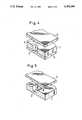
- a structure 1consists of walls with one and preferably several cavities therein to contain small amounts of substance, and the block is closed off with a cover 3.
- the block 1 and the cover 3are made of crystalline material such as semiconductor material.
- a counterpiece, cover 3is generated with a second mask which has humps 4 corresponding to the depressions 2, since the masks are geometrically identical.
- the mask techniquepermits high precision in production; it is known per se from semiconductor technology.
- the container in FIG. 1can be produced on (100) silicon, where the laterally limiting (111) planes make an angle of 54.7° to the wafer surface
- the inventionis not limited to the abovementioned etching technique.
- Other known kinds of making depressions in semiconductor or similar crystalline materialscan be applied such as laser beam drilling.
- the cover 3can be provided with a hump 4 which has the same 54.7° inclination to the crystal surface as the container block 1 in the area 2 and therefore seals perfectly tight. This is true also if the cover has a multiplicity of humps and the block 1 a multiplicity of depressions 2. If the fitting accuracy of the humps and depressions at the cover 3 and the block 1, made by the etching method are not sufficient for specific applications of particularly dangerous substances, a circular seal can be used in addition.
- FIG. 5shows an embodiment which in turn corresponds to the 54.7° inclination of the hump form of the cover and form a closure with a further inclination.
- adhesives or other joining techniquescan be used for increasing the tightness.
- a laser beamcan also be used with a seam welding process at the circular rim of the cover.
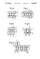
- a multiplicity of cavities 2is not limited as far as size, design and distribution in the block of the container.
- the cavities 2may, in particular, be square, rectangular, circular, oval or diamond-shaped. They can be tapered or expanded toward the body, see FIG. 1 and FIG. 2, or keep the same cross section if drilled, for instance, with a laser beam (FIG. 4). They can have also other cross sections or shapes (openings, canals).
- An additional layer or plate 5serves as a carrier or intermediate carrier (removable) advantageously of the same material, for instance, silicon or the like, as the body of the container, likewise providing a hermetically tight closure.
- the bottom 5is further covered, as shown in FIG. 6, with a layer 7 which may be, for instance, a filter layer, a sedimentation layer, an inert or catalytic or otherwise reacting layer of a material or only absorbing material.
- a layer 7which may be, for instance, a filter layer, a sedimentation layer, an inert or catalytic or otherwise reacting layer of a material or only absorbing material.
- a fiber fleece or a woven fleece with large pores and a large open surface, a fiber layout, foam material or a similar permeable structurecan be used, depending on the application (collecting, storing, reacting). This may involve a neutral carrier material or an active carrier material which is used for the layer 7 and underneath valves for further devices (see FIG. 8) can be used for the layer 7.
- the block 1 with the cavities 2contains them advantageously according to a raster measure in an X-Y distribution over the surface of the preferred silicon crystal as an array or in matrix form (see FIG. 3) so that they can be filled, gassed, injected, thinned, depleted, suctioned off or the like, for instance, by means of automatic devices, mixed or brought to reaction.
- the supply or discharge organsare then program-controlled line by line until the entire surface is scanned, as known per se, in automatic analyzers or automatic handling devices or robots for medical or other research purposes.
- the material of block 1must in any case be inert against the substance which is to be examined, treated, thinned or mixed. Or is to be the subject of a reaction or is to be tested for a particular result or the lack thereof.
- the cavities for examining or storingcan be made larger especially if the cavities 2 in block 1 are only part of sampling or examination or reaction chambers-see FIG. 7.
- the matrix or array arrangement in the X-Y directionis retained as described above and also the essentially sandwich-like construction according to FIG. 6.
- a further fitting depression 8 or 9which substantially increases overall the chamber volume or the volume of cavity 2. Then the supply and removal of a medium can then take place also in the plane of the drawing if, for instance, the same medium is to be supplied to or removed from all chambers.
- substances like solids in a fluidare examined for the purposes mentioned at the outset; gases in a liquid or gases or liquid in a solid can be examined. This is true especially for immune reactions, for the examination of enzymes or microorganisms.
- chemical or physical properties or their changescan be ascertained with respect to one or more properties like flow, density, surface or limit effects, especially features or particles, permeability, friction and adhesion.
- storage under certain conditionssuch as pressure or vacuum can be examined over a definite time or a reaction or a failure of a reaction to arrive.
- External influencescan be: radiation, heat treatment, application of reagents, the measurement of the change of material properties under heat, cold, steam, moisture or materials/particles supplied, through the application of electrical/electrochemical or magnetic means, through the application of sound, infrasound, ultrasound.
- calorimetric, spectrophotometric or fluorometric investigationsfor instance, using reagent layers such as litmus paper can be carried out as layer 7.
- Heating and/or cooling elementscan be taken to the chambers in the form of specifically annealed media in canals 10 and 11, for instance, through the plates 3 and 5 or thermocouples, particularly Peltier elements can be arranged at least partially in the vicinity of these cavities.
- Substancescan be provided with fluorescent markings, with radioactive markings or with enzyme markings with carriers or without carriers, bound or separable, organic or inorganic, with cells or cell fragments, gels or others can be used for detecting microorganisms, bacteria, viruses and others but also for detecting cancer, for determining individual substances in the blood or for determining the pH values, of blood sugar, of blood cholesterol or for detecting narcotics or others in the blood.
- Suitable methods of analysis particularly biological/medical, chemical/physical onesare known, especially for blood analysis, for the analysis of sera, etc.
- examination methods or other body liquidssuch as lymph liquid, urine, etc. are known, depending on whether small particles, marked or unmarked, organic/inorganic, with or without carriers of known type are used.
- a layer 7, as in FIG. 6can be arranged in the bottom 5.
- a further carrier or termination plate 14can be arranged which can also comprise a pickup device, for instance, photo cells in the same array arrangement for passing on for evaluation to a micro processor (not shown here).
- the lines for the supply and discharge of substances, reagents etc.are not shown, neither are the radiation sources which advantageously radiate in FIG. 8 from above, i.e., above the cover 3.
- Parts 3 and 5can also consist in FIG.
- cover 8advantageously of glass, silica or silicon ceramic or a composite silicon material and can be at least partially transparent and have at least partially mirror surfaces.
- the cover or the bottomcan be replaced optionally by strips of foil of light-impervious material at least in part; for instance, a plastic foil which brings about a hermetically tight seal but can be pierced by a hollow needle can also be cemented over the cover 3 if the latter contains the micro valves.
- Foils or layersmay be optically transparent or opaque; they can be realized as heating layers 10 or heat sinks 11 or made for optical purposes reflecting-nonreflecting, transparent, as filters, partially transparent or similarly for certain wavelengths. Also carbon or diamond layers and/or mask layers which cover the cavities at times or in part, can be used.
- the microvalvescan be addressed and driven in a manner known per se or be designed as described in German Patent Application P 38 11 052.0-31.
- the reaction in the cavitiescan then take place by movement, for instance, piezoelectrically, magnetically, electrostatically or in similar ways.
- a nutrient solution, a mutant, a reagent or similar substances diluted or enrichedcan be dosed and the dwelling time can be controlled by respective closing and opening of the microvalve.
- the heat or cooling treatmentcan be carried out by means of Peltier elements, heat pipes, Thomson-Joule coolers or similar means.
- Silicon sensorsare again preferred as sensors, arranged in the same array in the lowermost layer, particularly for the examination of physical or chemical properties such as black/white or gray value, contrast blurring, transmission, transparency, reflection, conductivity, resistivity, capacity, pressure, elongation, temperature volume, quantity, time, etc.
- the measured valuesare passed on to a microprocessor or microcomputer, now shown.
- the readoutcan be achieved in a manner known per se if the evaluation takes place optically, for instance, in a manner of the above application P 38 17 153.8-33.
- the storage and documentation of the data of the measuring or test program as well as the storage of, for instance, patient data or illness data, or data of sera or pharmaceuticalscan take place on the same chip (lowest layer in FIGS. 8 to 10).
- the storagecan be achieved either by means of an optical memory, for instance, according to DE-OS 3 804 751 with amorphous silicon as the storage medium (bubble memory) or as an integrated semiconductor memory (DE-OS 38 17 153) or with a RAM component (P 37 01 295.9-52).
- a light waveguide 15which passes through the micro chamber or cavity 2 in the block 1 or extends to it.
- the V-moat with its subareas 15a, 15bis changed at a 90° angle for showing subareas, but the light waveguide or optical fiber is longitudinal within the same axis as the V-moat if it passes through the cavity.
- the light waveguideis arranged so that it can distribute light into the cavity to evaluate changes in decoupled light under test-influences, i.e. by measuring transmitted light intensity.
- the lightcan be transmitted between (see FIG. 12) or through the optical fiber or waveguide longitudinally (see FIG. 9) and/or transverse to its axis (i.e. in an arrangement as shown in FIG. 10).
- the light waveguidecan be used as an information transmitter (bus) for evaluation in a (micro-)processor or (micro-)computer as in German patent 36 19 778.
- the mantle of the optical fiber or waveguideis partially destroyed or deterred in a region to get in contact with the substance to be tested or a substrate therefore.
- the mantlecan be chemically etched off (if of glass) or mechanically peeled off, by a tool (if the mantle is made of plastic).
- Modifications of the embodiment according to FIG. 9are possible in various ways, particularly for the photoelectric or other optoelectric evaluation not only by means of light waveguides.
- the light waveguidespreferably in V-moats, are arranged fixed resting on their bottoms and not only continuously but also cut off at an angle corresponding to the inclination of the moat.
- the waveguide arrangementcan be made parallel to the moat, transversely to the moat from above or from below at a 90° angle, 180° or similarly.
- the light waveguideswill bring light in and out to the cavity and are connected for test evaluation (of the substance) to photocells such as line sensors or arrays for the purpose of analog or preferably digital readout.
- the readoutcan take place in lines and rows, for instance, by means of scanners with the aid of a photoelectric line sensor as described in DE-OS 3 804 200.
- Transmitters and receivers, especially PIN diodes,can be integrated in the structural unit.
- the V-angle of the moatsare adjustable or variable as to slope (see DE-OS 3 613 181).
- Integrated optical waveguides and their design and applicationare described in the journal Laser and Optoelectronik, No. 4, 1986, pages 323 to 336. On page 338 of the same journal, application of light waveguide sensors in medicine are described.
- FIG. 10is shown a block 1 with bottom 5 and cover 3 and with microcavities 2 especially enlarged by recesses in the cover 3 and bottom 5, similar to FIG. 7, where however, above the microcavity 2 located in the array arrangement, treatment openings, valves, supply and discharge organs, windows, doping zones, etc. according to the chamber volume are disposed in the cover 3, while in the bottom 5, for instance, an array of photoelectric cells or a CCD array or a MOS field effect transistor is arranged which is connected for readout and evaluation, for instance, via the above mentioned optical or an electric bus to an evaluation unit, especially with microprocessors, of the microcomputers.
- an array of photoelectric cells or a CCD array or a MOS field effect transistoris arranged which is connected for readout and evaluation, for instance, via the above mentioned optical or an electric bus to an evaluation unit, especially with microprocessors, of the microcomputers.
- a light pen 16scans the array line- and column-wise, for instance, in binary code 8 ⁇ 8 microcavities or cells, respectively, or 10 ⁇ 10 for direct digital interrogation.
- a piezoelectric, a capacitive, a magnetic or an electric sensorcan find application.
- the pen 16is then suitable for applying a voltage, power or light irradiation or something similar, through the windows 17 in the cover 3 into the chambers 2 of the block 1 for direct readout, for instance, via a CCD array in the same arrangement as the microcavities or cells, indicated here by the CCD cells 17'.
- a MOSFET or a RAM componentcan be arranged.
- the readoutcan also be carried out with components or integrated optics, especially contactless and two-dimensionally (see DE OS 3 605 018 or U.S. Pat. No. 4,778,989).
- an ion-selective measuring electrodecan also be used as a replaceable sensor element, particularly for measuring the ion activities in liquids and at textile surfaces.
- Such ion-selective measuring systemsare known and are on the market. They are based on a purely electrical evaluation system in contrast to the embodiment of FIG. 9 which is used, for instance, for the optical determination of the catalytic enzyme activity of a substance sample where the change, due to the enzymic reaction of spectral properties of an enzyme substrate or its reaction products per unit time are picked up.
- the enzyme substrateis correlated with the exposed region of a light waveguide, with which the sample substance to be measured is brought into contact.
- an evaluation by means of a CCD arrayis advisable, for instance, according to DE-OS 3 817 153 or by means of semiconductors according to DE-OS 3 715 674 or by means of liquid crystal elements such as described, for instance, in German Patent 3,602,796.
- liquid crystal elementssuch as described, for instance, in German Patent 3,602,796.
- biosensorsare shown which are adapted to the properties to be examined and are generally known under the term "biosensors".
- biosensorswork generally with field-effects transistors 18 in silicon technology.
- the biosensorhas here a biological component on the surface which is connected to the gate of a transistor.
- This biological component or the reaction or enzyme substrate 19must be able to carry out the respectively desired reaction.
- voltage sources U1, U2voltage can be applied to a drain and source and corresponding changes in the event of ion activity.
- the measurementcan take place, according to FIG. 12, also photoelectrically, integrated, by means of a light waveguide between the transmitter and receivers such as diodes and lasers
- a biosensor of the kind under discussion hereis described in German Patent 3 634 573.
- a sensor on a silicon wafer 20is shown purely schematically, where a sensor chip 21 is brought to reaction with a substance specimen, for instance, a soil sample, a liquid sample, a food sample or a textile sample with toxic substances contained therein, the percentage of which, for instance, needs to be determined.
- a substance specimenfor instance, a soil sample, a liquid sample, a food sample or a textile sample with toxic substances contained therein, the percentage of which, for instance, needs to be determined.
- the required amount of oxygen or the oxygen content or something similarcan also be determined.
- the sensoris a conventional thermistor or a conductivity sensor. Also sound or ultrasound or infrasound sensors are suitable if the sample is to be subjected thereto. Miniature microphones are known for use therewith.
- FIG. 14an embodiment of an automatic tester is shown.
- a microcomputer or microprocessortakes over the control of the test procedure in accordance with a predetermined test program.
- the programmay contain interchangeably external memories, for instance, in a P EPROM or an erasable write-read memory.
- Patient data of the material to be tested, the reagents, etc.are likewise stored from, upon and after the completion of a test and the test results are likewise stored in the microcomputer or microprocessor, especially in one for freely selectable intervention, and the recording itself is documented, for instance, as a CCD picture, a heat image or on magnetic tape piezoresistively, electrostatically or ferroelectrically, etc.
- a film carrier 23is shown on which macrochips from a multiplicity of individual chips according to FIGS. 1 to 5 are cemented or are fastened detachably, wherein the film carrier has transport perforations 24 in order to conduct the film with the conventional film transports such as a Maltese Cross from roll to roll, is controlled via a treatment time of the program, and from station to station 25, i.e., here I-X.
- one or more substancesare first filled, according to a test program, into the microcavities of the chips in station I; in station II, a reaction then takes place either with or without treatment, and at the end of the reaction time measurement takes place automatically and passage into the test station III, so that optionally further tests can be carried out and the test results may be correlated automatically with the individual cavities and optionally with individual sample substances as well as patients.
- the self-documentation and storagetakes place in the microcomputer or microprocessor 22 for the automatic test control and test application.
- the inventionfurther provides apparatus for a micromechanical heat exchanger, especially a Joule-Thomson cooler.
- a Joule-Thomson cooler available on the market(for instance, from the firm Hymatik) has a very long metal helix which is wound on the surface of a cone.
- the overall arrangementis contained in a Dewar housing where the expanded gas flows back over a large area via the metal spiral between the Dewar wall and the cone surface provided with cooling fins.
- the inventionattacks the problem of providing a miniaturized heat exchanger, especially a Joule-Thomson cooler which can be manufactured cost-effectively and furnishes increased exchanger performance.
- the flow canals of a plate heat exchangerare arranged vertically in a thin substrate.
- This substrateis enclosed (in sandwich fashion) by two cover plates into which connecting canals are worked which close the vertical canals of the substrate as seen in the cross section, to form a meander.
- the individual cells of the heat exchangerare arranged in spiral shape on the substrate (as seen from above).
- At the center of the substratethere is an expansion chamber in which the main cooling output is generated.
- the highly compressed gasmeanders from the outside to the inside on the heat exchanger spiral, expands in the second expansion chamber and is then brought to the outside again counterflowwise via canals with substantially expanded cross section, already precooling the inflowing gas.
- the inventionis suitable in particular for cooling infrared CCDs.
- the highly compressed gasfor instance, nitrogen
- the boiling point of the gascan be reached (in the central expansion chamber of the gas) as the limit temperature.
- FIG. 15shows a cross section through a heat exchanger as a Joule-Thomson cooler in the vicinity of the high-pressure canals
- FIG. 16shows a top view of an elementary heat exchanger cell of the Joule-Thomson cooler in the area of the central silicon disc;
- FIG. 17shows a cross section through the Joule-Thomson cooler in the vicinity of the low-pressure canals, and in
- FIG. 18shows an overall arrangement of the elementary heat exchanger cells as well as of the expansion chamber at the center of the silicon disc.
- the overall arrangementconsists of three machined silicon discs 1, 1a, 1b which are connected to each other, and two cover plates, for instance, of glass 3, 5 which in turn are connected to the silicon discs according to FIG. 1.
- FIG. 15shows a cross section of the overall arrangement through the smaller cooling canals 26.
- depressions 27are etched which close the canals of the central silicon disc to form meanders. These depressions are likewise etched into (110) silicon discs, their depths being limited automatically by the crystallography. The etching is accomplished anisotropically by a batch process.
- the central silicon discInto the central silicon disc are worked vertical canals 26 which carry the outflowing and returning gas and at the same time serve as heat exchangers through the thin partitions.
- One elementary cell of this heat exchangeris shown in FIG. 16.
- the inner smaller canals 26carry the compressed outflowing gas (for instance, typically to 50 to 100 bar).
- the outer large canals 29are connected to each other so that they form a canal with a large cross section for the returning expanded gas.
- the partitions in the outer region 28merely have the purpose to take care of a heat exchange as effective as possible and of mechanical stability.
- the more strongly designed wall between the high and low pressure canalsmust take up the entire pressure difference and at the same time make possible a good heat transfer.
- the specific geometry of the canalsis due to the crystalline structure of silicon, with vertical (111)--planes on (110)--discs.
- FIG. 17shows a cross section through the outer region of the canals 29 for the returning gas.
- the outer silicon discs 1a and 1bare etched through completely in order to obtain a cross section as large as possible for the meanders of the expanded gas.
- FIG. 18The overall arrangement of the individual heat exchanger cells on the central silicon disc is shown in FIG. 18.
- the cellsare arranged side by side and are brought in spiral fashion from the outer region into the center of the disc.
- an expansion chamber 31In the center of the disc there is an expansion chamber 31, in which the cooling output is generated.
- On top of this chambera silicon chip or a similar semiconductor or ICs can be arranged, for instance, directly.
- the individual spiral armsare thermally insulated from each other by separation canals 32, 33.
- the novel micromechanical Joule-Thomson cooleris distinguished from the existing systems primarily due to the fact that it can be produced substantially more cheaper by the known batch process methods of micromechanics such as are used in the manufacture of semiconductor components. Furthermore, due to the vertical arrangement of the cooling canals and the frequent meanders, very high turbulence of the gas and therefore high efficiency of the heat exchanger can be expected. Furthermore, a semiconductor chip to be cooled can be integrated directly into the system or overall arrangement so that the cold output is generated directly at the chip without further partitions.
- the inventionis not limited to the use of a certain medium for the heat exchange.
- the conduction of the mediais not limited to the embodiment shown. Heat pipes can also be used.
Landscapes
- Chemical & Material Sciences (AREA)
- Health & Medical Sciences (AREA)
- Analytical Chemistry (AREA)
- General Health & Medical Sciences (AREA)
- Chemical Kinetics & Catalysis (AREA)
- Hematology (AREA)
- Clinical Laboratory Science (AREA)
- Physics & Mathematics (AREA)
- Biochemistry (AREA)
- Life Sciences & Earth Sciences (AREA)
- General Physics & Mathematics (AREA)
- Immunology (AREA)
- Pathology (AREA)
- Dispersion Chemistry (AREA)
- Spectroscopy & Molecular Physics (AREA)
- Organic Chemistry (AREA)
- Apparatus Associated With Microorganisms And Enzymes (AREA)
Abstract
Description
This is a continuation, of application Ser. No. 359,713, filed May 31, 1989, entitled Micromechanical Structure.
The present invention relates to a micromechanical structure for purposes of biotechnology, gene technology, cell research, pharmacology for healing and research on sicknesses which have been uncurable to date, also for agriculture research, to open up new sources of nutrition and energy and to restore the environment, for purposes of medicine, for instance, blood analysis but also of tissue and cells, for instance, antibody, antigen immobilization for preparing monoclonal antibodies, for preparing antibiotics, insulin and also for medications, sera, bacterial and other substance investigations and comparison tests. There is always the problem of safely controlled handling of the respective substance during and after an investigation, reaction or the like, especially if the substances can constitute a danger for the environment.
To meet the purposes mentioned above, particularly for fighting sickness and hunger in the world, it is necessary to be able to safely handle, in investigations, reactions, tests, comparison investigation and investigation series with, in particular, dangerous substances, also if the amounts of substance are ever so small.
It is an object of the present invention to facilitate or ensure clean, safe storage and handling of substances which are dangerous or could become so, be it prior to, during or after an investigation, reaction, test or the like
The above and other objects of the invention are achieved by a micromechanical structure with cavities, for investigating sample substances for possible changes of physical and/or chemical properties and/or bio-chemical properties, evaluation and documentation in a targeted manner for the purposes of biotechnology, gene technology, cell and immunity research and other medical, agricultural and environment research, wherein the structure comprises at least one of the group of semiconductive material (of the group III to V of the elements of the periodic system), glass, ceramic, diamond or carbon and is made by a masking technique, particularly by chemical etching techniques.
This microstructure has many advantages. It can be produced cost-effectively in large quantities. It is suitable for the safe storage for a multiplicity of substances such as samples for tests, for treatments, for investigation, for comparisons, for reactions, etc. The arrangement of suitable cavities relative to each other in the structure in the manner of a matrix or an array permits simple process control and the carrying-out of desired reactions, of desired small amounts of substance as well as their targeted treatment and examination. The structure with the cavities consists of inert material, i.e., it does not change in the investigations and treatments; the cavities can be closed off reliably and are not attacked by most toxic substances.
The invention will be described in greater detail in the following detailed description with reference to the drawings, in which:
FIG. 1 shows a structure with a single cavity and a definite surface orientation of the crystalline material;
FIG. 2 shows a modification of FIG. 1;
FIG. 3 shows a structure of crystalline material;
FIG. 4 shows a structure as a modification of FIG. 3;
FIG. 5 shows a structure in a design modification of FIG. 1;
FIG. 6 shows a modification of FIG. 2 or 4, where a structured portion in the center between portions different therefrom is arranged (sandwich construction);
FIG. 7 shows a modification of FIG. 6 with devices additionally arranged in the bottom plate and cover plate;
FIG. 8 shows a further modification of FIG. 6 or 7 with additional layers or plates;
FIG. 9 shows a design with a measuring or pickup device;
FIG. 10 shows a structure with a measuring and pickup device as well, optionally with memory;
FIG. 11 shows a device with a biosensor, especially a field-effect transistor;
FIG. 12 shows a modification of the embodiment according to FIG. 1;
FIG. 13 shows a device for ascertaining given substances in fluids;
FIG. 14 shows a device for automatic examination with documentation of the examination results;
FIG. 15 shows a heat exchanger, especially a plate cooler;
FIG. 16 is a top view of FIG. 15;
FIG. 17 is modification of FIG. 15; and
FIG. 18 is top view of FIG. 17.
As shown in FIG. 1, astructure 1 consists of walls with one and preferably several cavities therein to contain small amounts of substance, and the block is closed off with acover 3. Theblock 1 and thecover 3 are made of crystalline material such as semiconductor material. Likewise, for closing off the container according to the invention, a counterpiece,cover 3, is generated with a second mask which hashumps 4 corresponding to thedepressions 2, since the masks are geometrically identical. The mask technique permits high precision in production; it is known per se from semiconductor technology.
With the mentioned technique it is an advantage to apply an anisotropic etching method depending on the crystal orientation because thereby, utilizing the self-limiting action of (111) crystal planes, depressions with high geometric precision and very narrow tolerances can be realized. The container in FIG. 1 can be produced on (100) silicon, where the laterally limiting (111) planes make an angle of 54.7° to the wafer surface The invention is not limited to the abovementioned etching technique. Other known kinds of making depressions in semiconductor or similar crystalline materials can be applied such as laser beam drilling.
Thecover 3 can be provided with ahump 4 which has the same 54.7° inclination to the crystal surface as thecontainer block 1 in thearea 2 and therefore seals perfectly tight. This is true also if the cover has a multiplicity of humps and theblock 1 a multiplicity ofdepressions 2. If the fitting accuracy of the humps and depressions at thecover 3 and theblock 1, made by the etching method are not sufficient for specific applications of particularly dangerous substances, a circular seal can be used in addition. FIG. 5 shows an embodiment which in turn corresponds to the 54.7° inclination of the hump form of the cover and form a closure with a further inclination. In addition, adhesives or other joining techniques can be used for increasing the tightness. In particular, a laser beam can also be used with a seam welding process at the circular rim of the cover. A multiplicity ofcavities 2 is not limited as far as size, design and distribution in the block of the container.
The cavities 2 (and the humps 4) may, in particular, be square, rectangular, circular, oval or diamond-shaped. They can be tapered or expanded toward the body, see FIG. 1 and FIG. 2, or keep the same cross section if drilled, for instance, with a laser beam (FIG. 4). They can have also other cross sections or shapes (openings, canals).
An additional layer orplate 5 serves as a carrier or intermediate carrier (removable) advantageously of the same material, for instance, silicon or the like, as the body of the container, likewise providing a hermetically tight closure.
Thestructure 1 worked out from a block material advantageously (for mass production) forms a plane plate with throughcavities 2 such as openings, canals or the like of desired shape etched by wet chemistry, advantageously from silicon, while thecover 3 and thebottom 5 consist of material which can be joined preferably well to this material of thestructure 1, especially of material which can be sealed off hermetically tight such as glass, silica, glass ceramic or synthetic silicon or silicon metal compound material.
In FIG. 6, thebottom 5 is further covered, as shown in FIG. 6, with a layer 7 which may be, for instance, a filter layer, a sedimentation layer, an inert or catalytic or otherwise reacting layer of a material or only absorbing material. A fiber fleece or a woven fleece with large pores and a large open surface, a fiber layout, foam material or a similar permeable structure can be used, depending on the application (collecting, storing, reacting). This may involve a neutral carrier material or an active carrier material which is used for the layer 7 and underneath valves for further devices (see FIG. 8) can be used for the layer 7. Theblock 1 with thecavities 2 contains them advantageously according to a raster measure in an X-Y distribution over the surface of the preferred silicon crystal as an array or in matrix form (see FIG. 3) so that they can be filled, gassed, injected, thinned, depleted, suctioned off or the like, for instance, by means of automatic devices, mixed or brought to reaction. The supply or discharge organs are then program-controlled line by line until the entire surface is scanned, as known per se, in automatic analyzers or automatic handling devices or robots for medical or other research purposes.
The material ofblock 1 must in any case be inert against the substance which is to be examined, treated, thinned or mixed. Or is to be the subject of a reaction or is to be tested for a particular result or the lack thereof.
Depending on the purpose for which the invention is applied, the cavities for examining or storing (storage containers) can be made larger especially if thecavities 2 inblock 1 are only part of sampling or examination or reaction chambers-see FIG. 7. The matrix or array arrangement in the X-Y direction is retained as described above and also the essentially sandwich-like construction according to FIG. 6. In addition, there is correlated in thecover plate 3 and thebottom plate 5, with the respective cavity, a furtherfitting depression cavity 2. Then the supply and removal of a medium can then take place also in the plane of the drawing if, for instance, the same medium is to be supplied to or removed from all chambers.
As a rule, substances like solids in a fluid are examined for the purposes mentioned at the outset; gases in a liquid or gases or liquid in a solid can be examined. This is true especially for immune reactions, for the examination of enzymes or microorganisms. In examinations or analyses of substance/mixtures, chemical or physical properties or their changes can be ascertained with respect to one or more properties like flow, density, surface or limit effects, especially features or particles, permeability, friction and adhesion. In the simplest case, storage under certain conditions such as pressure or vacuum can be examined over a definite time or a reaction or a failure of a reaction to arrive. External influences can be: radiation, heat treatment, application of reagents, the measurement of the change of material properties under heat, cold, steam, moisture or materials/particles supplied, through the application of electrical/electrochemical or magnetic means, through the application of sound, infrasound, ultrasound. In addition, calorimetric, spectrophotometric or fluorometric investigations, for instance, using reagent layers such as litmus paper can be carried out as layer 7. Heating and/or cooling elements can be taken to the chambers in the form of specifically annealed media incanals plates microvalves bottom 5 ofblock 1 with themicro properties 2. The micro valves themselves are known per so (see, for instance,European Patent 0 250 948 A2). They are preferably arranged in the same array or in the same matrix in the X-Y direction as thecavities 2 in theblock 1 and thereby yield a simple evaluation possibility for respective examinations. A layer 7, as in FIG. 6 can be arranged in thebottom 5. Underneath thebottom 5, a further carrier ortermination plate 14 can be arranged which can also comprise a pickup device, for instance, photo cells in the same array arrangement for passing on for evaluation to a micro processor (not shown here). The lines for the supply and discharge of substances, reagents etc. are not shown, neither are the radiation sources which advantageously radiate in FIG. 8 from above, i.e., above thecover 3.Parts cover 3 if the latter contains the micro valves. Foils or layers may be optically transparent or opaque; they can be realized as heating layers 10 orheat sinks 11 or made for optical purposes reflecting-nonreflecting, transparent, as filters, partially transparent or similarly for certain wavelengths. Also carbon or diamond layers and/or mask layers which cover the cavities at times or in part, can be used.
The microvalves can be addressed and driven in a manner known per se or be designed as described in German Patent Application P 38 11 052.0-31. The reaction in the cavities can then take place by movement, for instance, piezoelectrically, magnetically, electrostatically or in similar ways. There, a nutrient solution, a mutant, a reagent or similar substances diluted or enriched can be dosed and the dwelling time can be controlled by respective closing and opening of the microvalve. The heat or cooling treatment can be carried out by means of Peltier elements, heat pipes, Thomson-Joule coolers or similar means.
Silicon sensors are again preferred as sensors, arranged in the same array in the lowermost layer, particularly for the examination of physical or chemical properties such as black/white or gray value, contrast blurring, transmission, transparency, reflection, conductivity, resistivity, capacity, pressure, elongation, temperature volume, quantity, time, etc. For evaluation, the measured values are passed on to a microprocessor or microcomputer, now shown. The readout can be achieved in a manner known per se if the evaluation takes place optically, for instance, in a manner of the above application P 38 17 153.8-33.
The storage and documentation of the data of the measuring or test program as well as the storage of, for instance, patient data or illness data, or data of sera or pharmaceuticals can take place on the same chip (lowest layer in FIGS. 8 to 10). The storage can be achieved either by means of an optical memory, for instance, according toDE-OS 3 804 751 with amorphous silicon as the storage medium (bubble memory) or as an integrated semiconductor memory (DE-OS 38 17 153) or with a RAM component (P 37 01 295.9-52). As is shown in FIG. 9, it is possible in a simple manner to use in the optical or optoelectronic evaluation, alight waveguide 15 which passes through the micro chamber orcavity 2 in theblock 1 or extends to it.
In FIG. 9 the V-moat with itssubareas
Preferably the light waveguide is arranged so that it can distribute light into the cavity to evaluate changes in decoupled light under test-influences, i.e. by measuring transmitted light intensity.
The light can be transmitted between (see FIG. 12) or through the optical fiber or waveguide longitudinally (see FIG. 9) and/or transverse to its axis (i.e. in an arrangement as shown in FIG. 10).
The light waveguide can be used as an information transmitter (bus) for evaluation in a (micro-)processor or (micro-)computer as in German patent 36 19 778.
As can be seen in FIG. 9 too, the mantle of the optical fiber or waveguide is partially destroyed or deterred in a region to get in contact with the substance to be tested or a substrate therefore.
The mantle can be chemically etched off (if of glass) or mechanically peeled off, by a tool (if the mantle is made of plastic).
Modifications of the embodiment according to FIG. 9 are possible in various ways, particularly for the photoelectric or other optoelectric evaluation not only by means of light waveguides. The light waveguides, preferably in V-moats, are arranged fixed resting on their bottoms and not only continuously but also cut off at an angle corresponding to the inclination of the moat. The waveguide arrangement can be made parallel to the moat, transversely to the moat from above or from below at a 90° angle, 180° or similarly. The light waveguides will bring light in and out to the cavity and are connected for test evaluation (of the substance) to photocells such as line sensors or arrays for the purpose of analog or preferably digital readout. The readout can take place in lines and rows, for instance, by means of scanners with the aid of a photoelectric line sensor as described inDE-OS 3 804 200. Transmitters and receivers, especially PIN diodes, can be integrated in the structural unit. The V-angle of the moats are adjustable or variable as to slope (see DE-OS 3 613 181). Integrated optical waveguides and their design and application are described in the journal Laser and Optoelectronik, No. 4, 1986, pages 323 to 336. On page 338 of the same journal, application of light waveguide sensors in medicine are described.
In FIG. 10 is shown ablock 1 withbottom 5 andcover 3 and withmicrocavities 2 especially enlarged by recesses in thecover 3 andbottom 5, similar to FIG. 7, where however, above themicrocavity 2 located in the array arrangement, treatment openings, valves, supply and discharge organs, windows, doping zones, etc. according to the chamber volume are disposed in thecover 3, while in thebottom 5, for instance, an array of photoelectric cells or a CCD array or a MOS field effect transistor is arranged which is connected for readout and evaluation, for instance, via the above mentioned optical or an electric bus to an evaluation unit, especially with microprocessors, of the microcomputers. Alight pen 16 scans the array line- and column-wise, for instance, inbinary code 8×8 microcavities or cells, respectively, or 10×10 for direct digital interrogation. Instead of thelight pen 16, a piezoelectric, a capacitive, a magnetic or an electric sensor can find application. Thepen 16 is then suitable for applying a voltage, power or light irradiation or something similar, through thewindows 17 in thecover 3 into thechambers 2 of theblock 1 for direct readout, for instance, via a CCD array in the same arrangement as the microcavities or cells, indicated here by the CCD cells 17'. Similarly, also a MOSFET or a RAM component can be arranged. The readout can also be carried out with components or integrated optics, especially contactless and two-dimensionally (seeDE OS 3 605 018 or U.S. Pat. No. 4,778,989). Instead of thelight pen 16, an ion-selective measuring electrode can also be used as a replaceable sensor element, particularly for measuring the ion activities in liquids and at textile surfaces. Such ion-selective measuring systems are known and are on the market. They are based on a purely electrical evaluation system in contrast to the embodiment of FIG. 9 which is used, for instance, for the optical determination of the catalytic enzyme activity of a substance sample where the change, due to the enzymic reaction of spectral properties of an enzyme substrate or its reaction products per unit time are picked up. The enzyme substrate is correlated with the exposed region of a light waveguide, with which the sample substance to be measured is brought into contact.
In the embodiment according to FIG. 10, an evaluation by means of a CCD array is advisable, for instance, according toDE-OS 3 817 153 or by means of semiconductors according toDE-OS 3 715 674 or by means of liquid crystal elements such as described, for instance, in German Patent 3,602,796. With such elements, direct storage of a test or analysis result is possible and can be interrogated in targeted fashion at any time, also as to individual microcavities.
In FIGS. 11 and 12, optoelectronic/electronic sensors are shown which are adapted to the properties to be examined and are generally known under the term "biosensors". Such biosensors work generally with field-effects transistors 18 in silicon technology. Produced together, the biosensor has here a biological component on the surface which is connected to the gate of a transistor. This biological component or the reaction orenzyme substrate 19 must be able to carry out the respectively desired reaction. Then, after the operating range is optimally adjusted, for instance, at R by means of one or more voltage sources U1, U2, voltage can be applied to a drain and source and corresponding changes in the event of ion activity. The measurement can take place, according to FIG. 12, also photoelectrically, integrated, by means of a light waveguide between the transmitter and receivers such as diodes and lasers A biosensor of the kind under discussion here is described inGerman Patent 3 634 573.
In FIG. 13, a sensor on asilicon wafer 20 is shown purely schematically, where a sensor chip 21 is brought to reaction with a substance specimen, for instance, a soil sample, a liquid sample, a food sample or a textile sample with toxic substances contained therein, the percentage of which, for instance, needs to be determined. The required amount of oxygen or the oxygen content or something similar can also be determined. The sensor is a conventional thermistor or a conductivity sensor. Also sound or ultrasound or infrasound sensors are suitable if the sample is to be subjected thereto. Miniature microphones are known for use therewith.
In FIG. 14, an embodiment of an automatic tester is shown. A microcomputer or microprocessor takes over the control of the test procedure in accordance with a predetermined test program. The program may contain interchangeably external memories, for instance, in a P EPROM or an erasable write-read memory. Patient data of the material to be tested, the reagents, etc. are likewise stored from, upon and after the completion of a test and the test results are likewise stored in the microcomputer or microprocessor, especially in one for freely selectable intervention, and the recording itself is documented, for instance, as a CCD picture, a heat image or on magnetic tape piezoresistively, electrostatically or ferroelectrically, etc.
In the embodiment according to FIG. 14, afilm carrier 23 is shown on which macrochips from a multiplicity of individual chips according to FIGS. 1 to 5 are cemented or are fastened detachably, wherein the film carrier has transport perforations 24 in order to conduct the film with the conventional film transports such as a Maltese Cross from roll to roll, is controlled via a treatment time of the program, and from station tostation 25, i.e., here I-X. There, one or more substances are first filled, according to a test program, into the microcavities of the chips in station I; in station II, a reaction then takes place either with or without treatment, and at the end of the reaction time measurement takes place automatically and passage into the test station III, so that optionally further tests can be carried out and the test results may be correlated automatically with the individual cavities and optionally with individual sample substances as well as patients. The self-documentation and storage takes place in the microcomputer or microprocessor 22 for the automatic test control and test application.
The invention further provides apparatus for a micromechanical heat exchanger, especially a Joule-Thomson cooler.
According to the present state of the art, there are available on the market various designs of miniaturized heat exchangers such as Joule-Thomson coolers. They are all 8 distinguished by very high unit costs.
A Joule-Thomson cooler available on the market (for instance, from the firm Hymatik) has a very long metal helix which is wound on the surface of a cone. The overall arrangement is contained in a Dewar housing where the expanded gas flows back over a large area via the metal spiral between the Dewar wall and the cone surface provided with cooling fins.
Another arrangement which was published by W. A. Little (AIP Proceedings for Future Trends in Superconductive Electronics, page 421, University of Virginia, Charlottesville, 1978), consists of several glass plates cemented together, into which lateral cooling canals had been worked. These coolers are not very effective since due to the poor thermal conductivity of the glass, the efficiency of the heat exchanger is limited.
The invention attacks the problem of providing a miniaturized heat exchanger, especially a Joule-Thomson cooler which can be manufactured cost-effectively and furnishes increased exchanger performance.
This problem is solved by the provision that in contrast to known designs, the flow canals of a plate heat exchanger are arranged vertically in a thin substrate. This substrate is enclosed (in sandwich fashion) by two cover plates into which connecting canals are worked which close the vertical canals of the substrate as seen in the cross section, to form a meander. The individual cells of the heat exchanger are arranged in spiral shape on the substrate (as seen from above). At the center of the substrate there is an expansion chamber in which the main cooling output is generated. The highly compressed gas meanders from the outside to the inside on the heat exchanger spiral, expands in the second expansion chamber and is then brought to the outside again counterflowwise via canals with substantially expanded cross section, already precooling the inflowing gas. So that the large radial temperature gradient over the substrate can be maintained and to minimize the losses due to heat conduction in the substrate and in the cover plates, vertical separation canals are worked in between the individual arms of the spirals. The overall arrangement is provided at top and bottom with two insulating plates with heat conduction as small as possible (for instance, glass). Glass cover plates can also be connected directly to the central plate (in sandwich fashion).
The invention is suitable in particular for cooling infrared CCDs. As the cooling medium, the highly compressed gas (for instance, nitrogen) is used where the boiling point of the gas can be reached (in the central expansion chamber of the gas) as the limit temperature.
The invention will be explained in the following, making reference to the embodiment shown in the drawing, where
FIG. 15 shows a cross section through a heat exchanger as a Joule-Thomson cooler in the vicinity of the high-pressure canals;
FIG. 16 shows a top view of an elementary heat exchanger cell of the Joule-Thomson cooler in the area of the central silicon disc;
FIG. 17 shows a cross section through the Joule-Thomson cooler in the vicinity of the low-pressure canals, and in
FIG. 18 shows an overall arrangement of the elementary heat exchanger cells as well as of the expansion chamber at the center of the silicon disc.
In the following, one embodiment of the Joule-Thomson cooler will be described. The overall arrangement consists of three machinedsilicon discs glass
FIG. 15 shows a cross section of the overall arrangement through thesmaller cooling canals 26. Into the upper and lower silicon discs,depressions 27 are etched which close the canals of the central silicon disc to form meanders. These depressions are likewise etched into (110) silicon discs, their depths being limited automatically by the crystallography. The etching is accomplished anisotropically by a batch process.
Into the central silicon disc are workedvertical canals 26 which carry the outflowing and returning gas and at the same time serve as heat exchangers through the thin partitions. One elementary cell of this heat exchanger is shown in FIG. 16. The innersmaller canals 26 carry the compressed outflowing gas (for instance, typically to 50 to 100 bar). The outerlarge canals 29 are connected to each other so that they form a canal with a large cross section for the returning expanded gas. The partitions in theouter region 28 merely have the purpose to take care of a heat exchange as effective as possible and of mechanical stability. The more strongly designed wall between the high and low pressure canals must take up the entire pressure difference and at the same time make possible a good heat transfer. In this embodiment, the specific geometry of the canals is due to the crystalline structure of silicon, with vertical (111)--planes on (110)--discs.
FIG. 17 shows a cross section through the outer region of thecanals 29 for the returning gas. There, theouter silicon discs
The overall arrangement of the individual heat exchanger cells on the central silicon disc is shown in FIG. 18. The cells are arranged side by side and are brought in spiral fashion from the outer region into the center of the disc. In the center of the disc there is anexpansion chamber 31, in which the cooling output is generated. On top of this chamber a silicon chip or a similar semiconductor or ICs can be arranged, for instance, directly. The individual spiral arms are thermally insulated from each other byseparation canals
The novel micromechanical Joule-Thomson cooler is distinguished from the existing systems primarily due to the fact that it can be produced substantially more cheaper by the known batch process methods of micromechanics such as are used in the manufacture of semiconductor components. Furthermore, due to the vertical arrangement of the cooling canals and the frequent meanders, very high turbulence of the gas and therefore high efficiency of the heat exchanger can be expected. Furthermore, a semiconductor chip to be cooled can be integrated directly into the system or overall arrangement so that the cold output is generated directly at the chip without further partitions.
The invention is not limited to the use of a certain medium for the heat exchange. In addition, the conduction of the media is not limited to the embodiment shown. Heat pipes can also be used.
In the foregoing specification, the invention has been described with reference to specific exemplary embodiments thereof. It will, however, be evident that various modifications and changes may be made thereunto without departing from the broader spirit and scope of the invention as set forth in the appended claims. The specification and drawings are, accordingly, to be regarded in an illustrative rather than in a restrictive sense.
Claims (15)
1. A micromechanical structure for investigation of sample substances in a targeted manner, comprising a masked-formed, etched structure with a plurality of depressions formed in an array that is made of at least one of a group of semiconductive materials, glass, ceramic, diamond, and carbon, the masked-formed, etched structure including a bottom structure, which has a plurality of depressions formed in an array, and a lid structure, which has a plurality of humps formed in an array, the lid and bottom structures being formed so the plurality of depressions and humps are at corresponding positions and have a same geometry, and so that when the lid structure is combined with the bottom structure, the plurality of corresponding depressions and humps are in alignment and form a plurality of microcontainments for containing one or more sample substances for evaluation and/or documentation of possible changes in one or more properties of the sample substances.
2. The micromechanical structure recited in claim 1, wherein the lid and bottom structures comprise the same material.
3. The micromechanical structure recited in claim 1, wherein the lid and bottom structures comprise silicon or another microcrystalline material or glass.
4. The micromechanical structure recited in claim 1, wherein the plurality of depressions are of defined form, size, arrangement, and distribution, and are in a surface of the bottom structure facing the lid structure.
5. The micromechanical structure recited in claim 4, wherein the lid structure fits hermetically tight on the bottom structure.
6. The micromechanical structure recited in claim 4, wherein the plurality of depressions are arranged in a predetermined spiral pattern.
7. The micromechanical structure recited in claim 4, wherein the lid structure has openings arranged in a same array as the depressions in the bottom structure, with the openings being capable of being closed, and wherein the lid structure further includes measuring and evaluating means for connection to computer means.
8. The micromechanical structure recited in claim 7, wherein the measuring and evaluating means are selected from the group consisting of optical, opto-electronic, electronic, piezoelectric, ferritic, magnetic, capacitive, ohmic or other measuring devices.
9. The micromechanical structure recited in claim 8, wherein the measuring and evaluating means are for individual measurements and evaluations of the individual contents of each of the plurality of depressions.
10. The micromechanical structure recited in claim 4, wherein a light waveguide distributes light into the plurality of depressions through the lid and bottom structures to evaluate changes in decoupled light by measuring transmitted intensity.
11. The micromechanical structure recited in claim 4, wherein the masked-formed, etched structure further comprises a detector for measuring external influences on the content of the individual depressions of the plurality of depressions.
12. The micromechanical structure recited in claim 1, wherein the arrangement of the plurality of depressions is provided in the array in matrix form, so that the matrix can be scanned by automatic filling or discharge and/or mixing and/or diluting/dosing means.
13. The micromechanical structure recited in claim 12, wherein the masked-formed, etched structure further comprises a plurality of microvalves which form a matrix which can be scanned in accordance with a predetermined program, the microvalves being arranged in the same array as the plurality of depressions.
14. The micromechanical structure recited in claim 1, wherein at least one depression of the plurality of depressions comprises a bio-sensor and/or biological-chemical sensor which includes a transistor containing a source and drain with a gate control.
15. The micromechanical structure recited in claim 1, wherein several of the masked-formed, etched structures are fixed onto a film carrier for transporting to a plurality of stations for automatic testing and evaluation.
Priority Applications (1)
| Application Number | Priority Date | Filing Date | Title |
|---|---|---|---|
| US07/830,755US5252294A (en) | 1988-06-01 | 1992-02-03 | Micromechanical structure |
Applications Claiming Priority (6)
| Application Number | Priority Date | Filing Date | Title |
|---|---|---|---|
| DE3818614 | 1988-06-01 | ||
| DE3818614ADE3818614A1 (en) | 1988-06-01 | 1988-06-01 | Microcontainer |
| JP3825907 | 1988-07-29 | ||
| DE3825907ADE3825907A1 (en) | 1988-07-29 | 1988-07-29 | Micromechanically fabricated cooling device, especially plate coolers |
| US35971389A | 1989-05-31 | 1989-05-31 | |
| US07/830,755US5252294A (en) | 1988-06-01 | 1992-02-03 | Micromechanical structure |
Related Parent Applications (1)
| Application Number | Title | Priority Date | Filing Date |
|---|---|---|---|
| US35971389AContinuation | 1988-06-01 | 1989-05-31 |
Publications (1)
| Publication Number | Publication Date |
|---|---|
| US5252294Atrue US5252294A (en) | 1993-10-12 |
Family
ID=27434226
Family Applications (1)
| Application Number | Title | Priority Date | Filing Date |
|---|---|---|---|
| US07/830,755Expired - Fee RelatedUS5252294A (en) | 1988-06-01 | 1992-02-03 | Micromechanical structure |
Country Status (1)
| Country | Link |
|---|---|
| US (1) | US5252294A (en) |
Cited By (163)
| Publication number | Priority date | Publication date | Assignee | Title |
|---|---|---|---|---|
| US5362975A (en)* | 1992-09-02 | 1994-11-08 | Kobe Steel Usa | Diamond-based chemical sensors |
| US5439647A (en)* | 1994-02-25 | 1995-08-08 | Fiberchem, Inc. | Chip level waveguide sensor |
| WO1995026796A1 (en)* | 1994-04-01 | 1995-10-12 | Integrated Chemical Synthesizers, Inc. | Integrated chemical synthesizers |
| WO1996003206A1 (en)* | 1994-07-25 | 1996-02-08 | E.I. Du Pont De Nemours And Company | Chemical mixing and reaction apparatus and processes for the preparation thereof |
| WO1996015450A1 (en)* | 1994-11-10 | 1996-05-23 | David Sarnoff Research Center, Inc. | A partitioned microelectronic device array |
| WO1996041864A1 (en)* | 1995-06-13 | 1996-12-27 | The Regents Of The University Of California | Diode laser heated micro-reaction chamber with sample detection means |
| US5589136A (en)* | 1995-06-20 | 1996-12-31 | Regents Of The University Of California | Silicon-based sleeve devices for chemical reactions |
| WO1997002357A1 (en)* | 1995-06-29 | 1997-01-23 | Affymetrix, Inc. | Integrated nucleic acid diagnostic device |
| WO1997012063A1 (en)* | 1995-09-28 | 1997-04-03 | Mathies Richard A | Miniature reaction chamber and devices incorporating same |
| US5639423A (en)* | 1992-08-31 | 1997-06-17 | The Regents Of The University Of Calfornia | Microfabricated reactor |
| US5659195A (en)* | 1995-06-08 | 1997-08-19 | The Regents Of The University Of California | CMOS integrated microsensor with a precision measurement circuit |
| US5716825A (en)* | 1995-11-01 | 1998-02-10 | Hewlett Packard Company | Integrated nucleic acid analysis system for MALDI-TOF MS |
| WO1998025701A1 (en) | 1996-12-11 | 1998-06-18 | The Regents Of The University Of California | Microfabricated sleeve devices for chemical reactions |
| US5770440A (en)* | 1995-06-27 | 1998-06-23 | Becton Dickinson And Company | Apparatus for the early detection of microorganisms |
| WO1998040726A1 (en)* | 1997-03-14 | 1998-09-17 | Trustees Of Tufts College | Fiber optic sensor with encoded microspheres |
| WO1998050147A1 (en)* | 1997-05-09 | 1998-11-12 | The Regents Of The University Of California | Peltier-assisted microfabricated reaction chambers for thermal cycling |
| US5840256A (en)* | 1996-04-09 | 1998-11-24 | David Sarnoff Research Center Inc. | Plate for reaction system |
| US5842787A (en)* | 1997-10-09 | 1998-12-01 | Caliper Technologies Corporation | Microfluidic systems incorporating varied channel dimensions |
| WO1999015895A1 (en)* | 1997-09-24 | 1999-04-01 | Sven Oscarsson | Method of arraying nanoparticles and macromolecules on surfaces |
| US5904424A (en)* | 1995-03-30 | 1999-05-18 | Merck Patent Gesellschaft Mit Beschrankter Haftung | Device for mixing small quantities of liquids |
| WO2000037606A1 (en)* | 1998-12-21 | 2000-06-29 | Corning Incorporated | An apparatus and method of making for holding and growing cells for processes interconnection |
| US6096656A (en)* | 1999-06-24 | 2000-08-01 | Sandia Corporation | Formation of microchannels from low-temperature plasma-deposited silicon oxynitride |
| US6143248A (en)* | 1996-08-12 | 2000-11-07 | Gamera Bioscience Corp. | Capillary microvalve |
| US6143247A (en)* | 1996-12-20 | 2000-11-07 | Gamera Bioscience Inc. | Affinity binding-based system for detecting particulates in a fluid |
| US6168948B1 (en) | 1995-06-29 | 2001-01-02 | Affymetrix, Inc. | Miniaturized genetic analysis systems and methods |
| US6171850B1 (en)* | 1999-03-08 | 2001-01-09 | Caliper Technologies Corp. | Integrated devices and systems for performing temperature controlled reactions and analyses |
| WO2001030490A1 (en)* | 1999-10-22 | 2001-05-03 | Aclara Biosciences, Inc. | Sealing for microfluidic devices |
| WO2001046493A1 (en)* | 1999-12-21 | 2001-06-28 | Gyros Ab | Polycrystalline diamond microstructures |
| US6261431B1 (en) | 1998-12-28 | 2001-07-17 | Affymetrix, Inc. | Process for microfabrication of an integrated PCR-CE device and products produced by the same |
| US6302134B1 (en) | 1997-05-23 | 2001-10-16 | Tecan Boston | Device and method for using centripetal acceleration to device fluid movement on a microfluidics system |
| US20010046701A1 (en)* | 2000-05-24 | 2001-11-29 | Schulte Thomas H. | Nucleic acid amplification and detection using microfluidic diffusion based structures |
| WO2001034291A3 (en)* | 1999-11-09 | 2001-12-06 | Stanford Res Inst Int | High-throughput synthesis, screening and characterization of combinatorial libraries |
| US6338820B1 (en) | 1997-08-15 | 2002-01-15 | Alexion Pharmaceuticals, Inc. | Apparatus for performing assays at reaction sites |
| US20020015920A1 (en)* | 2000-08-07 | 2002-02-07 | Steinberg Dan A. | Fiber optic chip with lenslet array and method of fabrication |
| US20020022261A1 (en)* | 1995-06-29 | 2002-02-21 | Anderson Rolfe C. | Miniaturized genetic analysis systems and methods |
| WO2001064344A3 (en)* | 2000-03-02 | 2002-03-21 | Microchips Inc | Microfabricated devices for the storage and selective exposure of chemicals and devices |
| US6376233B1 (en)* | 1996-11-12 | 2002-04-23 | Micronas Intermetall Gmbh | Device for conducting research on cell specimens and similar materials |
| US20020048536A1 (en)* | 1999-03-03 | 2002-04-25 | Bergh H. Sam | Parallel flow process optimization reactors |
| US20020072784A1 (en)* | 2000-10-10 | 2002-06-13 | Sheppard Norman F. | Microchip reservoir devices using wireless transmission of power and data |
| US20020084565A1 (en)* | 2000-08-07 | 2002-07-04 | Dautartas Mindaugas F. | Alignment apparatus and method for aligning stacked devices |
| US6423552B1 (en)* | 1998-04-03 | 2002-07-23 | Zuhong Lu | Method for the preparation of compound micro array chips and the compound micro array chips produced according to said method |
| US20020128585A1 (en)* | 2000-07-07 | 2002-09-12 | Cork William H | Medical system, method and apparatus employing mems |
| US6458325B1 (en)* | 1996-11-25 | 2002-10-01 | Abb Limited | Apparatus for analyzing liquid samples automatically and continually |
| WO2002086479A1 (en)* | 2001-04-25 | 2002-10-31 | Centre National De La Recherche Scientifique | Biosensor matrix and method for making same |
| US20020187260A1 (en)* | 2001-05-30 | 2002-12-12 | Sheppard Norman F. | Conformal coated microchip reservoir devices |
| US20020197709A1 (en)* | 2001-06-22 | 2002-12-26 | Van Der Weide Daniel W. | Microfabricated microbial growth assay method and apparatus |
| US20020197456A1 (en)* | 1993-06-30 | 2002-12-26 | Pope Edward J. A. | Integrated electro-luminescent biochip |
| US20030010808A1 (en)* | 2001-06-28 | 2003-01-16 | Uhland Scott A. | Methods for hermetically sealing microchip reservoir devices |
| US6521187B1 (en) | 1996-05-31 | 2003-02-18 | Packard Instrument Company | Dispensing liquid drops onto porous brittle substrates |
| US6521181B1 (en)* | 1995-06-20 | 2003-02-18 | The Regents Of The University Of Calfornia | Microfabricated electrochemiluminescence cell for chemical reaction detection |
| US6527762B1 (en) | 1999-08-18 | 2003-03-04 | Microchips, Inc. | Thermally-activated microchip chemical delivery devices |
| US20030044320A1 (en)* | 2001-08-31 | 2003-03-06 | Shun Luo | High throughput screening micro array platform |
| US6537256B2 (en) | 1999-11-17 | 2003-03-25 | Microchips, Inc. | Microfabricated devices for the delivery of molecules into a carrier fluid |
| US6537817B1 (en) | 1993-05-31 | 2003-03-25 | Packard Instrument Company | Piezoelectric-drop-on-demand technology |
| US6544734B1 (en) | 1998-10-09 | 2003-04-08 | Cynthia G. Briscoe | Multilayered microfluidic DNA analysis system and method |
| US20030113935A1 (en)* | 2001-12-19 | 2003-06-19 | Carson Larry J. | Analytical device with lightguide illumination of capillary and microgrooves arrays |
| US6589779B1 (en) | 1999-07-16 | 2003-07-08 | Board Of Regents, The University Of Texas System | General signaling protocol for chemical receptors in immobilized matrices |
| EP1174182A4 (en)* | 1999-02-18 | 2003-07-23 | Toyo Kohan Co Ltd | Micro-chip for chemical reaction |
| EP1019696A4 (en)* | 1997-09-19 | 2003-07-23 | Aclara Biosciences Inc | LIQUID TRANSFER SYSTEM AND METHOD |
| US20030148401A1 (en)* | 2001-11-09 | 2003-08-07 | Anoop Agrawal | High surface area substrates for microarrays and methods to make same |
| US6605454B2 (en) | 1999-09-16 | 2003-08-12 | Motorola, Inc. | Microfluidic devices with monolithic microwave integrated circuits |
| US6613560B1 (en)* | 1994-10-19 | 2003-09-02 | Agilent Technologies, Inc. | PCR microreactor for amplifying DNA using microquantities of sample fluid |
| US20030186228A1 (en)* | 2000-01-31 | 2003-10-02 | Mcdevitt John T. | Portable sensor array system |
| US6632399B1 (en) | 1998-05-22 | 2003-10-14 | Tecan Trading Ag | Devices and methods for using centripetal acceleration to drive fluid movement in a microfluidics system for performing biological fluid assays |
| WO2003003754A3 (en)* | 2001-06-29 | 2003-10-23 | Vivactiss Bvba | Intelligent microplates with remote data access |
| WO2002073172A3 (en)* | 2001-03-09 | 2003-10-30 | Gnothis Holding Sa | Determination of analytes by means of fluorescence correlation spectroscopy |
| US20030232403A1 (en)* | 1999-06-18 | 2003-12-18 | Kellogg Gregory L. | Devices and methods for the performance of miniaturized homogeneous assays |
| WO2002083852A3 (en)* | 2001-04-10 | 2004-02-19 | Bioprocessors Corp | Microfermentor device and cell based screening method |
| US20040038647A1 (en)* | 1993-12-20 | 2004-02-26 | Intermec Technologies Corporation | Local area network having multiple channel wireless access |
| EP0897216A3 (en)* | 1997-08-11 | 2004-03-10 | Fraunhofer-Gesellschaft zur Förderung der angewandten Forschung e.V. | Piezoelectric resonator, its manufacturing method and its use as a sensor for measuring the concentration of a constituent in a fluid and/or defining the physical properties of the fluid |
| US20040048241A1 (en)* | 2001-06-11 | 2004-03-11 | Freeman Beverly Annette | Methods for attaching molecules |
| US20040065093A1 (en)* | 2000-12-07 | 2004-04-08 | Gunter Fuhr | Cryostorage method and device |
| EP1284158A3 (en)* | 2001-08-07 | 2004-04-14 | Eidgenössische Technische Hochschule Zürich | Microsensor system for monitoring biological and chemical processes |
| US6730072B2 (en) | 2000-05-30 | 2004-05-04 | Massachusetts Institute Of Technology | Methods and devices for sealing microchip reservoir devices |
| US20040106953A1 (en)* | 2002-10-04 | 2004-06-03 | Yomtov Barry M. | Medical device for controlled drug delivery and cardiac monitoring and/or stimulation |
| US20040106914A1 (en)* | 2002-09-23 | 2004-06-03 | Coppeta Jonathan R. | Micro-reservoir osmotic release systems and microtube array device |
| US20040121486A1 (en)* | 2002-08-16 | 2004-06-24 | Uhland Scott A. | Controlled release device and method using electrothermal ablation |
| WO2004060534A1 (en)* | 2002-12-18 | 2004-07-22 | Millipore Corporation | Combination laboratory device with multifunctionality |
| US20040146863A1 (en)* | 2001-06-11 | 2004-07-29 | Pisharody Sobha M. | Electronic detection of biological molecules using thin layers |
| US20040151631A1 (en)* | 2001-03-09 | 2004-08-05 | Rudolf Rigler | Determination of analytes by means of fluorescence correlation spectroscopy |
| US6773429B2 (en) | 2000-10-11 | 2004-08-10 | Microchips, Inc. | Microchip reservoir devices and facilitated corrosion of electrodes |
| WO2004071660A1 (en)* | 2003-02-14 | 2004-08-26 | Cytocentrics Ccs Gmbh | Method and device for contacting a microfluid structure |
| US20040247671A1 (en)* | 2003-04-25 | 2004-12-09 | Prescott James H. | Solid drug formulation and device for storage and controlled delivery thereof |
| US20040248320A1 (en)* | 1999-12-10 | 2004-12-09 | Santini John T. | Medical device with array of electrode-containing reservoirs |
| US20050002763A1 (en)* | 2003-04-30 | 2005-01-06 | Osram Opto Semiconductors Gmbh | Chip receptacle, method for fabricating a chip receptacle and chip transport container |
| US20050019902A1 (en)* | 1995-09-28 | 2005-01-27 | Mathies Richard A. | Miniaturized integrated nucleic acid processing and analysis device and method |
| US20050025670A1 (en)* | 2002-09-14 | 2005-02-03 | Sinsky Jerome L. | Diagnostic device and method of using same |
| WO2005012561A1 (en) | 2003-08-01 | 2005-02-10 | Capital Biochip Company Ltd. | Microarray devices having controllable reaction volume |
| US20050042149A1 (en)* | 1994-04-01 | 2005-02-24 | Integrated Chemical Synthesizers, Inc. | Nanoscale chemical synthesis |
| US20050055014A1 (en)* | 2003-08-04 | 2005-03-10 | Coppeta Jonathan R. | Methods for accelerated release of material from a reservoir device |
| US6875208B2 (en) | 2001-05-31 | 2005-04-05 | Massachusetts Institute Of Technology | Microchip devices with improved reservoir opening |
| US20050100946A1 (en)* | 1995-06-29 | 2005-05-12 | Affymetrix, Inc. | Integrated nucleic acid diagnostic device and method for in-situ confocal microscopy |
| US6908770B1 (en) | 1998-07-16 | 2005-06-21 | Board Of Regents, The University Of Texas System | Fluid based analysis of multiple analytes by a sensor array |
| US6908594B1 (en) | 1999-10-22 | 2005-06-21 | Aclara Biosciences, Inc. | Efficient microfluidic sealing |
| US6923939B1 (en)* | 2001-07-05 | 2005-08-02 | Uop Llc | Heat activated membrane introduction apparatus and method for screening materials |
| US20050186578A1 (en)* | 2004-02-20 | 2005-08-25 | Sven Bulow | Chamber array arrangement |
| US20050186585A1 (en)* | 2004-02-24 | 2005-08-25 | Thermal Gradient | Thermal cycling device |
| US20050191620A1 (en)* | 2004-02-27 | 2005-09-01 | Mcdevitt John T. | Particle on membrane assay system |
| US6976982B2 (en) | 2001-01-09 | 2005-12-20 | Microchips, Inc. | Flexible microchip devices for ophthalmic and other applications |
| WO2005118773A3 (en)* | 2004-05-28 | 2006-02-02 | Wafergen Inc | Apparatus and methods for multiplex analyses |
| US20060024358A1 (en)* | 2004-07-30 | 2006-02-02 | Santini John T Jr | Multi-reservoir device for transdermal drug delivery and sensing |
| US7022517B1 (en) | 1999-07-16 | 2006-04-04 | Board Of Regents, The University Of Texas System | Method and apparatus for the delivery of samples to a chemical sensor array |
| US20060073585A1 (en)* | 2002-07-24 | 2006-04-06 | Mcdevitt John T | Capture and detection of microbes by membrane methods |
| US20060084106A1 (en)* | 1993-10-28 | 2006-04-20 | Beattie Kenneth L | Microfabricated, flowthrough porous apparatus for discrete detection of binding reactions |
| US7033840B1 (en) | 1999-11-09 | 2006-04-25 | Sri International | Reaction calorimeter and differential scanning calorimeter for the high-throughput synthesis, screening and characterization of combinatorial libraries |
| US20060105275A1 (en)* | 2004-11-15 | 2006-05-18 | Maloney John M | Fabrication methods and structures for micro-reservoir devices |
| US20060115323A1 (en)* | 2004-11-04 | 2006-06-01 | Coppeta Jonathan R | Compression and cold weld sealing methods and devices |
| WO2006058816A1 (en)* | 2004-12-03 | 2006-06-08 | Fraunhofer-Gesellschaft zur Förderung der angewandten Forschung e.V. | Sample receiver for a cryogenic sample and associated analysis method |
| US7070590B1 (en) | 1996-07-02 | 2006-07-04 | Massachusetts Institute Of Technology | Microchip drug delivery devices |
| US20060159592A1 (en)* | 1998-05-08 | 2006-07-20 | Gyros Patent Ab | Microfluidic device |
| US20060194273A1 (en)* | 1998-04-27 | 2006-08-31 | Gyros Patent Ab | Microfabricated apparatus for cell based assays |
| US7118917B2 (en) | 2001-03-07 | 2006-10-10 | Symyx Technologies, Inc. | Parallel flow reactor having improved thermal control |
| US7122156B2 (en) | 2000-03-07 | 2006-10-17 | Symyx Technologies, Inc. | Parallel flow reactor having variable composition |
| US20060257854A1 (en)* | 2004-02-27 | 2006-11-16 | Mcdevitt John T | Membrane assay system including preloaded particles |
| US20060257991A1 (en)* | 2004-02-27 | 2006-11-16 | Mcdevitt John T | Integration of fluids and reagents into self-contained cartridges containing particle-based sensor elements and membrane-based sensor elements |
| US20060257941A1 (en)* | 2004-02-27 | 2006-11-16 | Mcdevitt John T | Integration of fluids and reagents into self-contained cartridges containing particle and membrane sensor elements |
| US20060263265A1 (en)* | 2005-05-23 | 2006-11-23 | Der-Ren Kang | Blood micro-separator |
| US20070054416A1 (en)* | 1997-06-26 | 2007-03-08 | Regnier Fred E | High density sample holder for analysis of biological samples |
| US20070088442A1 (en)* | 2005-10-14 | 2007-04-19 | Microchips, Inc. | Passive wear-indicating sensor for implantable prosthetic device |
| US20070099288A1 (en)* | 2005-11-02 | 2007-05-03 | Affymetrix, Inc. | Microfluidic Methods, Devices, and Systems for Fluid Handling |
| US20070111300A1 (en)* | 1996-04-03 | 2007-05-17 | Applera Corporation | Device and method for multiple analyte detection |
| US20070128084A1 (en)* | 1996-01-16 | 2007-06-07 | Affymetrix, Inc. | Analytical Biochemistry System with Robotically Carried Bioarray |
| US20070202531A1 (en)* | 2004-02-24 | 2007-08-30 | Joel Grover | Thermal Cycling Device |
| WO2007034374A3 (en)* | 2005-09-23 | 2007-09-07 | Koninkl Philips Electronics Nv | A micro-fluidic device based upon active matrix principles |
| US7297313B1 (en) | 1991-08-31 | 2007-11-20 | The Regents Of The University Of California | Microfabricated reactor, process for manufacturing the reactor, and method of amplification |
| US20070267782A1 (en)* | 2005-11-02 | 2007-11-22 | Affymetrix, Inc. | System and Method for Making Lab Card by Embossing |
| US20070275035A1 (en)* | 2006-05-24 | 2007-11-29 | Microchips, Inc. | Minimally Invasive Medical Implant Devices for Controlled Drug Delivery |
| US20080015494A1 (en)* | 2006-07-11 | 2008-01-17 | Microchips, Inc. | Multi-reservoir pump device for dialysis, biosensing, or delivery of substances |
| US20080038714A1 (en)* | 2005-11-02 | 2008-02-14 | Affymetrix, Inc. | Instrument to Pneumatically Control Lab Cards and Method Thereof |
| US20080044844A1 (en)* | 2004-01-27 | 2008-02-21 | Shimshon Belkin | Populations Of Cells And Devices And Systems Including Same |
| US20080076975A1 (en)* | 2005-01-25 | 2008-03-27 | Microchips, Inc. | Method and implantable device with reservoir array for pre-clinical in vivo testing |
| EP1972375A1 (en)* | 2007-03-23 | 2008-09-24 | Koninklijke Philips Electronics N.V. | A micro-fluidic device based upon active matrix principles |
| US20080288178A1 (en)* | 2001-08-24 | 2008-11-20 | Applera Corporation | Sequencing system with memory |
| US20080302659A1 (en)* | 2007-06-07 | 2008-12-11 | Microchips, Inc. | Electrochemical biosensors and arrays |
| US20080311585A1 (en)* | 2005-11-02 | 2008-12-18 | Affymetrix, Inc. | System and method for multiplex liquid handling |
| US7485454B1 (en) | 2000-03-10 | 2009-02-03 | Bioprocessors Corp. | Microreactor |
| US7488316B2 (en) | 2005-01-25 | 2009-02-10 | Microchips, Inc. | Control of drug release by transient modification of local microenvironments |
| US20090070337A1 (en)* | 2006-09-28 | 2009-03-12 | Xeround Systems Ltd. | Apparatus and method for a distributed storage global database |
| US20090145576A1 (en)* | 2005-08-11 | 2009-06-11 | Eksigent Technologies, Llc | Microfluid based apparatus and method for thermal regulation and noise reduction |
| US7599737B2 (en) | 2002-10-04 | 2009-10-06 | Microchips, Inc. | Medical device for neural stimulation and controlled drug delivery |
| US7604628B2 (en) | 2004-09-01 | 2009-10-20 | Microchips, Inc. | Multi-cap reservoir devices for controlled release or exposure of reservoir contents |
| US7622294B2 (en) | 1997-03-14 | 2009-11-24 | Trustees Of Tufts College | Methods for detecting target analytes and enzymatic reactions |
| US20090297403A1 (en)* | 2006-08-31 | 2009-12-03 | Volker Franke | Method for producing a bioreactor or lab-on-a-chip system and bioreactors or lab-on-a-chip systems produced therewith |
| US7651868B2 (en) | 2003-12-11 | 2010-01-26 | The Board Of Regents Of The University Of Texas System | Method and system for the analysis of saliva using a sensor array |
| US20100112719A1 (en)* | 2008-11-06 | 2010-05-06 | Amihood Doron | Electronic signal amplification in field effect device based chemical sensors |
| US20100307921A1 (en)* | 2001-09-19 | 2010-12-09 | Life Technologies Corporation | Microdevice with integrated memory |
| US20110220964A1 (en)* | 2010-03-12 | 2011-09-15 | Shin Dongsuk | Semiconductor device having field effect transistor and method for fabricating the same |
| US8075852B2 (en) | 2005-11-02 | 2011-12-13 | Affymetrix, Inc. | System and method for bubble removal |
| EP2397224A1 (en) | 2010-06-15 | 2011-12-21 | arrayon biotechnology S.A. | Apparatus and platform for multiplex analysis |
| US8095197B2 (en) | 2003-11-03 | 2012-01-10 | Microchips, Inc. | Medical device for sensing glucose |
| US8101431B2 (en) | 2004-02-27 | 2012-01-24 | Board Of Regents, The University Of Texas System | Integration of fluids and reagents into self-contained cartridges containing sensor elements and reagent delivery systems |
| US8105849B2 (en) | 2004-02-27 | 2012-01-31 | Board Of Regents, The University Of Texas System | Integration of fluids and reagents into self-contained cartridges containing sensor elements |
| US8252581B2 (en) | 2007-01-22 | 2012-08-28 | Wafergen, Inc. | Apparatus for high throughput chemical reactions |
| US8257967B2 (en) | 2002-04-26 | 2012-09-04 | Board Of Regents, The University Of Texas System | Method and system for the detection of cardiac risk factors |
| US8377398B2 (en) | 2005-05-31 | 2013-02-19 | The Board Of Regents Of The University Of Texas System | Methods and compositions related to determination and use of white blood cell counts |
| US8592220B2 (en) | 2006-10-26 | 2013-11-26 | Intermolecular, Inc. | High pressure parallel fixed bed reactor and method |
| US8665071B2 (en) | 2004-03-19 | 2014-03-04 | Applied Biosystems, Llc | Methods and systems for using RFID in biological field |
| US20140160900A1 (en)* | 2011-07-21 | 2014-06-12 | The Swatch Group Research And Development Ltd. | Functional micromechanical assembly |
| CN106124274A (en)* | 2016-08-09 | 2016-11-16 | 中国石油大学(北京) | Sanding gear for geologic structure physical modelling experiment |
| US10107804B2 (en) | 2001-03-23 | 2018-10-23 | Trustees Of Tufts College | Methods for detecting target analytes and enzymatic reactions |
| US10641772B2 (en) | 2015-02-20 | 2020-05-05 | Takara Bio Usa, Inc. | Method for rapid accurate dispensing, visualization and analysis of single cells |
| US11112416B2 (en) | 2018-01-30 | 2021-09-07 | Life Technologies Corporation | Instruments, devices and consumables for use in a workflow of a smart molecular analysis system |
| US11460405B2 (en) | 2016-07-21 | 2022-10-04 | Takara Bio Usa, Inc. | Multi-Z imaging and dispensing with multi-well devices |
Citations (14)
| Publication number | Priority date | Publication date | Assignee | Title |
|---|---|---|---|---|
| US3973320A (en)* | 1973-09-06 | 1976-08-10 | Giovanni Greco | Method for the production of semiconductor devices with an integral heatsink and of related semiconductor equipment |
| US4233029A (en)* | 1978-10-25 | 1980-11-11 | Eastman Kodak Company | Liquid transport device and method |
| DE3602796A1 (en)* | 1986-01-30 | 1987-08-06 | Messerschmitt Boelkow Blohm | SENSOR ELEMENT WITH A MEMORY FOR ABNORMAL CHANGES IN THE INCIDENT LIGHT INTENSITY |
| DE3613181A1 (en)* | 1986-04-18 | 1987-10-22 | Siemens Ag | METHOD FOR PRODUCING TRENCHES WITH ADJUSTABLE SLOPE OF THE TRENCH WALLS IN SEMICONDUCTOR SUBSTRATES MADE OF SILICON |
| EP0250948A2 (en)* | 1986-06-26 | 1988-01-07 | Fraunhofer-Gesellschaft Zur Förderung Der Angewandten Forschung E.V. | Microvalve |
| US4740410A (en)* | 1987-05-28 | 1988-04-26 | The Regents Of The University Of California | Micromechanical elements and methods for their fabrication |
| DE3701295A1 (en)* | 1987-01-17 | 1988-09-08 | Messerschmitt Boelkow Blohm | SENSOR FOR DETERMINING MEASURED SIZES |
| US4778989A (en)* | 1984-09-19 | 1988-10-18 | Siemens Aktiengesellschaft | Scanning device for microline-by-microline illumination and optically scanning a planar original |
| DE3715674A1 (en)* | 1987-05-11 | 1988-12-01 | Messerschmitt Boelkow Blohm | SEMICONDUCTOR WITH CAPACITIVE READING OF THE CARGO CARRIERS AND INTEGRATED DC VOLTAGE SUPPLY |
| DE3804751A1 (en)* | 1988-02-16 | 1989-08-24 | Messerschmitt Boelkow Blohm | Amorphous silicon as a storage medium |
| DE3804200A1 (en)* | 1988-02-11 | 1989-08-24 | Messerschmitt Boelkow Blohm | Photoelectric line sensor |
| US4874500A (en)* | 1987-07-15 | 1989-10-17 | Sri International | Microelectrochemical sensor and sensor array |
| DE3817153A1 (en)* | 1988-05-19 | 1989-11-30 | Messerschmitt Boelkow Blohm | SEMICONDUCTOR COMPONENT |
| US4895615A (en)* | 1988-03-09 | 1990-01-23 | Siemens Aktiengesellschaft | Monolithic fabrication techniques for front face optoelectronic couplers and/or optical components including ridge structured waveguides |
- 1992
- 1992-02-03USUS07/830,755patent/US5252294A/ennot_activeExpired - Fee Related
Patent Citations (14)
| Publication number | Priority date | Publication date | Assignee | Title |
|---|---|---|---|---|
| US3973320A (en)* | 1973-09-06 | 1976-08-10 | Giovanni Greco | Method for the production of semiconductor devices with an integral heatsink and of related semiconductor equipment |
| US4233029A (en)* | 1978-10-25 | 1980-11-11 | Eastman Kodak Company | Liquid transport device and method |
| US4778989A (en)* | 1984-09-19 | 1988-10-18 | Siemens Aktiengesellschaft | Scanning device for microline-by-microline illumination and optically scanning a planar original |
| DE3602796A1 (en)* | 1986-01-30 | 1987-08-06 | Messerschmitt Boelkow Blohm | SENSOR ELEMENT WITH A MEMORY FOR ABNORMAL CHANGES IN THE INCIDENT LIGHT INTENSITY |
| DE3613181A1 (en)* | 1986-04-18 | 1987-10-22 | Siemens Ag | METHOD FOR PRODUCING TRENCHES WITH ADJUSTABLE SLOPE OF THE TRENCH WALLS IN SEMICONDUCTOR SUBSTRATES MADE OF SILICON |
| EP0250948A2 (en)* | 1986-06-26 | 1988-01-07 | Fraunhofer-Gesellschaft Zur Förderung Der Angewandten Forschung E.V. | Microvalve |
| DE3701295A1 (en)* | 1987-01-17 | 1988-09-08 | Messerschmitt Boelkow Blohm | SENSOR FOR DETERMINING MEASURED SIZES |
| DE3715674A1 (en)* | 1987-05-11 | 1988-12-01 | Messerschmitt Boelkow Blohm | SEMICONDUCTOR WITH CAPACITIVE READING OF THE CARGO CARRIERS AND INTEGRATED DC VOLTAGE SUPPLY |
| US4740410A (en)* | 1987-05-28 | 1988-04-26 | The Regents Of The University Of California | Micromechanical elements and methods for their fabrication |
| US4874500A (en)* | 1987-07-15 | 1989-10-17 | Sri International | Microelectrochemical sensor and sensor array |
| DE3804200A1 (en)* | 1988-02-11 | 1989-08-24 | Messerschmitt Boelkow Blohm | Photoelectric line sensor |
| DE3804751A1 (en)* | 1988-02-16 | 1989-08-24 | Messerschmitt Boelkow Blohm | Amorphous silicon as a storage medium |
| US4895615A (en)* | 1988-03-09 | 1990-01-23 | Siemens Aktiengesellschaft | Monolithic fabrication techniques for front face optoelectronic couplers and/or optical components including ridge structured waveguides |
| DE3817153A1 (en)* | 1988-05-19 | 1989-11-30 | Messerschmitt Boelkow Blohm | SEMICONDUCTOR COMPONENT |
Non-Patent Citations (5)
| Title |
|---|
| Angell et al., "Silicon Micromechanical Devices", Apr. 1983, pp. 44-55. |
| Angell et al., Silicon Micromechanical Devices , Apr. 1983, pp. 44 55.* |
| Laser and Optoelectronik, No. 4, 1986, pp. 323 336.* |
| Laser and Optoelectronik, No. 4, 1986, pp. 323-336. |
| W. A. Little, AIP Proceedings for Future Trends in Superconductive Electronics, p. 421, 1978.* |
Cited By (332)
| Publication number | Priority date | Publication date | Assignee | Title |
|---|---|---|---|---|
| US7297313B1 (en) | 1991-08-31 | 2007-11-20 | The Regents Of The University Of California | Microfabricated reactor, process for manufacturing the reactor, and method of amplification |
| US7169601B1 (en) | 1992-08-31 | 2007-01-30 | The Regents Of The University Of California | Microfabricated reactor |
| US5646039A (en)* | 1992-08-31 | 1997-07-08 | The Regents Of The University Of California | Microfabricated reactor |
| US7935312B2 (en) | 1992-08-31 | 2011-05-03 | Regents Of The University Of California | Microfabricated reactor, process for manufacturing the reactor, and method of amplification |
| US5674742A (en)* | 1992-08-31 | 1997-10-07 | The Regents Of The University Of California | Microfabricated reactor |
| US5639423A (en)* | 1992-08-31 | 1997-06-17 | The Regents Of The University Of Calfornia | Microfabricated reactor |
| US5362975A (en)* | 1992-09-02 | 1994-11-08 | Kobe Steel Usa | Diamond-based chemical sensors |
| US6537817B1 (en) | 1993-05-31 | 2003-03-25 | Packard Instrument Company | Piezoelectric-drop-on-demand technology |
| US20020197456A1 (en)* | 1993-06-30 | 2002-12-26 | Pope Edward J. A. | Integrated electro-luminescent biochip |
| US20060084106A1 (en)* | 1993-10-28 | 2006-04-20 | Beattie Kenneth L | Microfabricated, flowthrough porous apparatus for discrete detection of binding reactions |
| US20040038647A1 (en)* | 1993-12-20 | 2004-02-26 | Intermec Technologies Corporation | Local area network having multiple channel wireless access |
| US5650123A (en)* | 1994-02-25 | 1997-07-22 | Fci-Fiberchem, Inc. | Chip level waveguide sensor |
| US5439647A (en)* | 1994-02-25 | 1995-08-08 | Fiberchem, Inc. | Chip level waveguide sensor |
| EP1203954A3 (en)* | 1994-04-01 | 2003-02-12 | Integrated Chemical Synthesizers, Inc. | Chemical reactions using a nanoscale reaction system |
| US5580523A (en)* | 1994-04-01 | 1996-12-03 | Bard; Allen J. | Integrated chemical synthesizers |
| WO1995026796A1 (en)* | 1994-04-01 | 1995-10-12 | Integrated Chemical Synthesizers, Inc. | Integrated chemical synthesizers |
| EP1550866A1 (en)* | 1994-04-01 | 2005-07-06 | Integrated Chemical Synthesizers, Inc. | Integrated chemical synthesizers |
| US20050042149A1 (en)* | 1994-04-01 | 2005-02-24 | Integrated Chemical Synthesizers, Inc. | Nanoscale chemical synthesis |
| WO1996003206A1 (en)* | 1994-07-25 | 1996-02-08 | E.I. Du Pont De Nemours And Company | Chemical mixing and reaction apparatus and processes for the preparation thereof |
| US6613560B1 (en)* | 1994-10-19 | 2003-09-02 | Agilent Technologies, Inc. | PCR microreactor for amplifying DNA using microquantities of sample fluid |
| US5755942A (en)* | 1994-11-10 | 1998-05-26 | David Sarnoff Research Center, Inc. | Partitioned microelectronic device array |
| WO1996015450A1 (en)* | 1994-11-10 | 1996-05-23 | David Sarnoff Research Center, Inc. | A partitioned microelectronic device array |
| US5904424A (en)* | 1995-03-30 | 1999-05-18 | Merck Patent Gesellschaft Mit Beschrankter Haftung | Device for mixing small quantities of liquids |
| US5659195A (en)* | 1995-06-08 | 1997-08-19 | The Regents Of The University Of California | CMOS integrated microsensor with a precision measurement circuit |
| WO1996041864A1 (en)* | 1995-06-13 | 1996-12-27 | The Regents Of The University Of California | Diode laser heated micro-reaction chamber with sample detection means |
| US6524532B1 (en) | 1995-06-20 | 2003-02-25 | The Regents Of The University Of California | Microfabricated sleeve devices for chemical reactions |
| US6521181B1 (en)* | 1995-06-20 | 2003-02-18 | The Regents Of The University Of Calfornia | Microfabricated electrochemiluminescence cell for chemical reaction detection |
| US5589136A (en)* | 1995-06-20 | 1996-12-31 | Regents Of The University Of California | Silicon-based sleeve devices for chemical reactions |
| US5770440A (en)* | 1995-06-27 | 1998-06-23 | Becton Dickinson And Company | Apparatus for the early detection of microorganisms |
| US6319468B1 (en) | 1995-06-27 | 2001-11-20 | Tecan Trading Ag | Affinity binding-based system for detecting particulates in a fluid |
| US5922591A (en)* | 1995-06-29 | 1999-07-13 | Affymetrix, Inc. | Integrated nucleic acid diagnostic device |
| US6197595B1 (en) | 1995-06-29 | 2001-03-06 | Affymetrix, Inc. | Integrated nucleic acid diagnostic device |
| US20050100946A1 (en)* | 1995-06-29 | 2005-05-12 | Affymetrix, Inc. | Integrated nucleic acid diagnostic device and method for in-situ confocal microscopy |
| US20060246490A1 (en)* | 1995-06-29 | 2006-11-02 | Affymetrix, Inc. | Miniaturized genetic analysis systems and methods |
| US6043080A (en)* | 1995-06-29 | 2000-03-28 | Affymetrix, Inc. | Integrated nucleic acid diagnostic device |
| US6168948B1 (en) | 1995-06-29 | 2001-01-02 | Affymetrix, Inc. | Miniaturized genetic analysis systems and methods |
| WO1997002357A1 (en)* | 1995-06-29 | 1997-01-23 | Affymetrix, Inc. | Integrated nucleic acid diagnostic device |
| US6830936B2 (en) | 1995-06-29 | 2004-12-14 | Affymetrix Inc. | Integrated nucleic acid diagnostic device |
| US5856174A (en)* | 1995-06-29 | 1999-01-05 | Affymetrix, Inc. | Integrated nucleic acid diagnostic device |
| US6326211B1 (en) | 1995-06-29 | 2001-12-04 | Affymetrix, Inc. | Method of manipulating a gas bubble in a microfluidic device |
| US20020022261A1 (en)* | 1995-06-29 | 2002-02-21 | Anderson Rolfe C. | Miniaturized genetic analysis systems and methods |
| US20050019902A1 (en)* | 1995-09-28 | 2005-01-27 | Mathies Richard A. | Miniaturized integrated nucleic acid processing and analysis device and method |
| US6284525B1 (en)* | 1995-09-28 | 2001-09-04 | Affymetrix, Inc. | Miniature reaction chamber and devices incorporating same |
| WO1997012063A1 (en)* | 1995-09-28 | 1997-04-03 | Mathies Richard A | Miniature reaction chamber and devices incorporating same |
| US6132580A (en)* | 1995-09-28 | 2000-10-17 | The Regents Of The University Of California | Miniature reaction chamber and devices incorporating same |
| US5716825A (en)* | 1995-11-01 | 1998-02-10 | Hewlett Packard Company | Integrated nucleic acid analysis system for MALDI-TOF MS |
| US8273304B2 (en) | 1996-01-16 | 2012-09-25 | Affymetrix, Inc. | Analytical biochemistry system with robotically carried bioarray |
| US20070128084A1 (en)* | 1996-01-16 | 2007-06-07 | Affymetrix, Inc. | Analytical Biochemistry System with Robotically Carried Bioarray |
| US20070111300A1 (en)* | 1996-04-03 | 2007-05-17 | Applera Corporation | Device and method for multiple analyte detection |
| US20110003281A1 (en)* | 1996-04-03 | 2011-01-06 | Applera Corporation | Device and method for multiple analyte detection |
| US8247219B2 (en) | 1996-04-03 | 2012-08-21 | Applied Biosystems, Llc | Device and method for multiple analyte detection |
| US8163538B2 (en) | 1996-04-03 | 2012-04-24 | Applied Biosystems, Llc | Device and method for multiple analyte detection |
| US20080102462A1 (en)* | 1996-04-03 | 2008-05-01 | Applera Corporation | Device and method for multiple analyte detection |
| US5840256A (en)* | 1996-04-09 | 1998-11-24 | David Sarnoff Research Center Inc. | Plate for reaction system |
| US6521187B1 (en) | 1996-05-31 | 2003-02-18 | Packard Instrument Company | Dispensing liquid drops onto porous brittle substrates |
| US7918842B2 (en) | 1996-07-02 | 2011-04-05 | Massachusetts Institute Of Technology | Medical device with controlled reservoir opening |
| US7070590B1 (en) | 1996-07-02 | 2006-07-04 | Massachusetts Institute Of Technology | Microchip drug delivery devices |
| US7892221B2 (en) | 1996-07-02 | 2011-02-22 | Massachusetts Institute Of Technology | Method of controlled drug delivery from implant device |
| US7901397B2 (en) | 1996-07-02 | 2011-03-08 | Massachusetts Institute Of Technology | Method for operating microchip reservoir device |
| US20080051766A1 (en)* | 1996-07-02 | 2008-02-28 | Massachusetts Institute Of Technology | Method for Operating Microchip Reservoir Device |
| US6143248A (en)* | 1996-08-12 | 2000-11-07 | Gamera Bioscience Corp. | Capillary microvalve |
| US20020150512A1 (en)* | 1996-08-12 | 2002-10-17 | Tecan Trading Ag. | Capillary microvalve |
| US6376233B1 (en)* | 1996-11-12 | 2002-04-23 | Micronas Intermetall Gmbh | Device for conducting research on cell specimens and similar materials |
| US6458325B1 (en)* | 1996-11-25 | 2002-10-01 | Abb Limited | Apparatus for analyzing liquid samples automatically and continually |
| WO1998025701A1 (en) | 1996-12-11 | 1998-06-18 | The Regents Of The University Of California | Microfabricated sleeve devices for chemical reactions |
| EP0948408A4 (en)* | 1996-12-11 | 2001-01-17 | Univ California | MINIATURIZED TUBE REACTOR FOR CHEMICAL REACTIONS |
| US6656430B2 (en) | 1996-12-20 | 2003-12-02 | Tecan Trading Ag | Affinity binding-based system for detecting particulates in a fluid |
| US6143247A (en)* | 1996-12-20 | 2000-11-07 | Gamera Bioscience Inc. | Affinity binding-based system for detecting particulates in a fluid |
| US10241026B2 (en) | 1997-03-14 | 2019-03-26 | Trustees Of Tufts College | Target analyte sensors utilizing microspheres |
| US9377388B2 (en) | 1997-03-14 | 2016-06-28 | Trustees Of Tufts College | Methods for detecting target analytes and enzymatic reactions |
| WO1998040726A1 (en)* | 1997-03-14 | 1998-09-17 | Trustees Of Tufts College | Fiber optic sensor with encoded microspheres |
| US7622294B2 (en) | 1997-03-14 | 2009-11-24 | Trustees Of Tufts College | Methods for detecting target analytes and enzymatic reactions |
| WO1998050147A1 (en)* | 1997-05-09 | 1998-11-12 | The Regents Of The University Of California | Peltier-assisted microfabricated reaction chambers for thermal cycling |
| US6302134B1 (en) | 1997-05-23 | 2001-10-16 | Tecan Boston | Device and method for using centripetal acceleration to device fluid movement on a microfluidics system |
| US6399361B2 (en) | 1997-05-23 | 2002-06-04 | Tecan Trading Ag | Devices and methods for using centripetal acceleration to drive fluid movement in a microfluidics system |
| US20040089616A1 (en)* | 1997-05-23 | 2004-05-13 | Gregory Kellogg | Devices and methods for using centripetal acceleration to drive fluid movement in a microfluidics system for performing biological fluid assays |
| US6548788B2 (en) | 1997-05-23 | 2003-04-15 | Tecan Trading Ag | Devices and methods for using centripetal acceleration to drive fluid movement in a microfluidics system |
| US20070054416A1 (en)* | 1997-06-26 | 2007-03-08 | Regnier Fred E | High density sample holder for analysis of biological samples |
| EP0897216A3 (en)* | 1997-08-11 | 2004-03-10 | Fraunhofer-Gesellschaft zur Förderung der angewandten Forschung e.V. | Piezoelectric resonator, its manufacturing method and its use as a sensor for measuring the concentration of a constituent in a fluid and/or defining the physical properties of the fluid |
| US6338820B1 (en) | 1997-08-15 | 2002-01-15 | Alexion Pharmaceuticals, Inc. | Apparatus for performing assays at reaction sites |
| EP1019696A4 (en)* | 1997-09-19 | 2003-07-23 | Aclara Biosciences Inc | LIQUID TRANSFER SYSTEM AND METHOD |
| WO1999015895A1 (en)* | 1997-09-24 | 1999-04-01 | Sven Oscarsson | Method of arraying nanoparticles and macromolecules on surfaces |
| US6517234B1 (en) | 1997-10-09 | 2003-02-11 | Caliper Technologies Corp. | Microfluidic systems incorporating varied channel dimensions |
| US5842787A (en)* | 1997-10-09 | 1998-12-01 | Caliper Technologies Corporation | Microfluidic systems incorporating varied channel dimensions |
| US6186660B1 (en) | 1997-10-09 | 2001-02-13 | Caliper Technologies Corp. | Microfluidic systems incorporating varied channel dimensions |
| US5957579A (en)* | 1997-10-09 | 1999-09-28 | Caliper Technologies Corp. | Microfluidic systems incorporating varied channel dimensions |
| WO1999019056A1 (en)* | 1997-10-09 | 1999-04-22 | Caliper Technologies Corporation | Microfluidic systems incorporating varied channel depths |
| AU737711B2 (en)* | 1997-10-09 | 2001-08-30 | Caliper Life Sciences, Inc. | Microfluidic systems incorporating varied channel depths |
| US6423552B1 (en)* | 1998-04-03 | 2002-07-23 | Zuhong Lu | Method for the preparation of compound micro array chips and the compound micro array chips produced according to said method |
| US20060194273A1 (en)* | 1998-04-27 | 2006-08-31 | Gyros Patent Ab | Microfabricated apparatus for cell based assays |
| US7935522B2 (en) | 1998-04-27 | 2011-05-03 | Gyros Patent Ab | Microfabricated apparatus for cell based assays |
| US8030062B2 (en) | 1998-04-27 | 2011-10-04 | Gyros Patent Ab | Microfabricated apparatus for cell based assays |
| US20060159592A1 (en)* | 1998-05-08 | 2006-07-20 | Gyros Patent Ab | Microfluidic device |
| US8722421B2 (en) | 1998-05-08 | 2014-05-13 | Gyros Patent Ab | Microfluidic device |
| US6632399B1 (en) | 1998-05-22 | 2003-10-14 | Tecan Trading Ag | Devices and methods for using centripetal acceleration to drive fluid movement in a microfluidics system for performing biological fluid assays |
| US6908770B1 (en) | 1998-07-16 | 2005-06-21 | Board Of Regents, The University Of Texas System | Fluid based analysis of multiple analytes by a sensor array |
| US7491552B2 (en) | 1998-07-16 | 2009-02-17 | The Board Of Regents Of The University Of Texas System | Fluid based analysis of multiple analytes by a sensor array |
| US6544734B1 (en) | 1998-10-09 | 2003-04-08 | Cynthia G. Briscoe | Multilayered microfluidic DNA analysis system and method |
| WO2000037606A1 (en)* | 1998-12-21 | 2000-06-29 | Corning Incorporated | An apparatus and method of making for holding and growing cells for processes interconnection |
| US6261431B1 (en) | 1998-12-28 | 2001-07-17 | Affymetrix, Inc. | Process for microfabrication of an integrated PCR-CE device and products produced by the same |
| EP1174182A4 (en)* | 1999-02-18 | 2003-07-23 | Toyo Kohan Co Ltd | Micro-chip for chemical reaction |
| US7150994B2 (en) | 1999-03-03 | 2006-12-19 | Symyx Technologies, Inc. | Parallel flow process optimization reactor |
| US20020048536A1 (en)* | 1999-03-03 | 2002-04-25 | Bergh H. Sam | Parallel flow process optimization reactors |
| US6337212B1 (en) | 1999-03-08 | 2002-01-08 | Caliper Technologies Corp. | Methods and integrated devices and systems for performing temperature controlled reactions and analyses |
| US6171850B1 (en)* | 1999-03-08 | 2001-01-09 | Caliper Technologies Corp. | Integrated devices and systems for performing temperature controlled reactions and analyses |
| US6541274B2 (en) | 1999-03-08 | 2003-04-01 | Caliper Technologies Corp. | Integrated devices and method of use for performing temperature controlled reactions and analyses |
| US20030232403A1 (en)* | 1999-06-18 | 2003-12-18 | Kellogg Gregory L. | Devices and methods for the performance of miniaturized homogeneous assays |
| US6096656A (en)* | 1999-06-24 | 2000-08-01 | Sandia Corporation | Formation of microchannels from low-temperature plasma-deposited silicon oxynitride |
| US7022517B1 (en) | 1999-07-16 | 2006-04-04 | Board Of Regents, The University Of Texas System | Method and apparatus for the delivery of samples to a chemical sensor array |
| US6589779B1 (en) | 1999-07-16 | 2003-07-08 | Board Of Regents, The University Of Texas System | General signaling protocol for chemical receptors in immobilized matrices |
| US6602702B1 (en)* | 1999-07-16 | 2003-08-05 | The University Of Texas System | Detection system based on an analyte reactive particle |
| US6669683B2 (en) | 1999-08-18 | 2003-12-30 | Microchips, Inc. | Thermally-activated microchip chemical delivery devices |
| US20090112188A1 (en)* | 1999-08-18 | 2009-04-30 | Microchips, Inc. | Device for controlling exposure of reservoir contents to surroundings |
| US8016817B2 (en) | 1999-08-18 | 2011-09-13 | Microchips, Inc. | Device for controlling exposure of reservoir contents to surroundings |
| US6527762B1 (en) | 1999-08-18 | 2003-03-04 | Microchips, Inc. | Thermally-activated microchip chemical delivery devices |
| US20040143236A1 (en)* | 1999-08-18 | 2004-07-22 | Santini John T. | Thermally-activated reservoir devices |
| US7473248B2 (en) | 1999-08-18 | 2009-01-06 | Microchips, Inc. | Thermally-activated reservoir devices |
| US6605454B2 (en) | 1999-09-16 | 2003-08-12 | Motorola, Inc. | Microfluidic devices with monolithic microwave integrated circuits |
| US6623945B1 (en) | 1999-09-16 | 2003-09-23 | Motorola, Inc. | System and method for microwave cell lysing of small samples |
| US6908594B1 (en) | 1999-10-22 | 2005-06-21 | Aclara Biosciences, Inc. | Efficient microfluidic sealing |
| WO2001030490A1 (en)* | 1999-10-22 | 2001-05-03 | Aclara Biosciences, Inc. | Sealing for microfluidic devices |
| US7033840B1 (en) | 1999-11-09 | 2006-04-25 | Sri International | Reaction calorimeter and differential scanning calorimeter for the high-throughput synthesis, screening and characterization of combinatorial libraries |
| WO2001034291A3 (en)* | 1999-11-09 | 2001-12-06 | Stanford Res Inst Int | High-throughput synthesis, screening and characterization of combinatorial libraries |
| US6602714B1 (en) | 1999-11-09 | 2003-08-05 | Sri International | Viscosity and mass sensor for the high-throughput synthesis, screening and characterization of combinatorial libraries |
| US6656162B2 (en) | 1999-11-17 | 2003-12-02 | Microchips, Inc. | Implantable drug delivery stents |
| US7041130B2 (en) | 1999-11-17 | 2006-05-09 | Boston Scientific Scimed, Inc. | Stent for controlled release of drug |
| US7052488B2 (en) | 1999-11-17 | 2006-05-30 | Boston Scientific Scimed, Inc. | Implantable drug delivery device |
| US6537256B2 (en) | 1999-11-17 | 2003-03-25 | Microchips, Inc. | Microfabricated devices for the delivery of molecules into a carrier fluid |
| US20040260391A1 (en)* | 1999-11-17 | 2004-12-23 | Santini John T. | Stent for controlled release of drug |
| US20040034332A1 (en)* | 1999-11-17 | 2004-02-19 | Uhland Scott A. | Implantable drug delivery device |
| US20040248320A1 (en)* | 1999-12-10 | 2004-12-09 | Santini John T. | Medical device with array of electrode-containing reservoirs |
| US7070592B2 (en) | 1999-12-10 | 2006-07-04 | Massachusetts Institute Of Technology | Medical device with array of electrode-containing reservoirs |
| WO2001046493A1 (en)* | 1999-12-21 | 2001-06-28 | Gyros Ab | Polycrystalline diamond microstructures |
| US20030186228A1 (en)* | 2000-01-31 | 2003-10-02 | Mcdevitt John T. | Portable sensor array system |
| US7316899B2 (en) | 2000-01-31 | 2008-01-08 | The Board Of Regents Of The University Of Texas System | Portable sensor array system |
| US6713298B2 (en)* | 2000-01-31 | 2004-03-30 | Board Of Regents, The University Of Texas System | Method and apparatus for the delivery of samples to a chemical sensor array |
| US20050136548A1 (en)* | 2000-01-31 | 2005-06-23 | Board Of Regents, The University Of Texas System | System and method for the analysis of bodily fluids |
| US20040053322A1 (en)* | 2000-01-31 | 2004-03-18 | Mcdevitt John T. | System and method for the analysis of bodily fluids |
| US6649403B1 (en)* | 2000-01-31 | 2003-11-18 | Board Of Regents, The University Of Texas Systems | Method of preparing a sensor array |
| US6551838B2 (en) | 2000-03-02 | 2003-04-22 | Microchips, Inc. | Microfabricated devices for the storage and selective exposure of chemicals and devices |
| US6849463B2 (en) | 2000-03-02 | 2005-02-01 | Microchips, Inc. | Microfabricated devices for the storage and selective exposure of chemicals and devices |
| US7614135B2 (en) | 2000-03-02 | 2009-11-10 | Microchips, Inc. | Method for making reservoir-based sensor device |
| US20070299385A1 (en)* | 2000-03-02 | 2007-12-27 | Microchips, Inc. | Device for the controlled exposure of reservoir-based sensors |
| US7410616B2 (en) | 2000-03-02 | 2008-08-12 | Microchips, Inc. | Device for the controlled exposure of reservoir-based sensors |
| AU2001252890B2 (en)* | 2000-03-02 | 2005-06-02 | Microchips, Inc. | Microfabricated devices for the storage and selective exposure of chemicals and devices |
| US20050124979A1 (en)* | 2000-03-02 | 2005-06-09 | Santini John T.Jr. | Device for release of chemical molecules using pressure-generated rupture of reservoirs |
| US7445766B2 (en) | 2000-03-02 | 2008-11-04 | Microchips, Inc. | Medical device and method for diagnostic sensing |
| WO2001064344A3 (en)* | 2000-03-02 | 2002-03-21 | Microchips Inc | Microfabricated devices for the storage and selective exposure of chemicals and devices |
| AU2005204238B2 (en)* | 2000-03-02 | 2007-05-31 | Microchips, Inc. | Microfabricated devices for the storage and selective exposure of chemicals and devices |
| US7648677B2 (en) | 2000-03-02 | 2010-01-19 | Microchips, Inc. | Method for operating a reservoir-based sensor device |
| US20080115361A1 (en)* | 2000-03-02 | 2008-05-22 | Microchips, Inc. | Method for Making Reservoir-Based Sensor Device |
| US20080115559A1 (en)* | 2000-03-02 | 2008-05-22 | Microchips, Inc. | Method for Operating a Reservoir-Based Sensor Device |
| US7122156B2 (en) | 2000-03-07 | 2006-10-17 | Symyx Technologies, Inc. | Parallel flow reactor having variable composition |
| US7485454B1 (en) | 2000-03-10 | 2009-02-03 | Bioprocessors Corp. | Microreactor |
| US20010046701A1 (en)* | 2000-05-24 | 2001-11-29 | Schulte Thomas H. | Nucleic acid amplification and detection using microfluidic diffusion based structures |
| US6730072B2 (en) | 2000-05-30 | 2004-05-04 | Massachusetts Institute Of Technology | Methods and devices for sealing microchip reservoir devices |
| US20050269250A1 (en)* | 2000-07-07 | 2005-12-08 | Cork William H | Medical system, method and apparatus employing MEMS |
| US20020128585A1 (en)* | 2000-07-07 | 2002-09-12 | Cork William H | Medical system, method and apparatus employing mems |
| US20050269251A1 (en)* | 2000-07-07 | 2005-12-08 | Cork William H | Medical system, method and apparatus employing MEMS |
| US6994781B2 (en) | 2000-07-07 | 2006-02-07 | Baxter International Inc. | Medical system, method and apparatus employing MEMS |
| US7217356B2 (en) | 2000-07-07 | 2007-05-15 | Fenwal, Inc. | Medical system, method and apparatus employing MEMS |
| US20060272149A1 (en)* | 2000-08-07 | 2006-12-07 | Shipley Company, L.L.C. | Alignment apparatus and method for aligning stacked devices |
| US7086134B2 (en) | 2000-08-07 | 2006-08-08 | Shipley Company, L.L.C. | Alignment apparatus and method for aligning stacked devices |
| US20020015920A1 (en)* | 2000-08-07 | 2002-02-07 | Steinberg Dan A. | Fiber optic chip with lenslet array and method of fabrication |
| US7290321B2 (en) | 2000-08-07 | 2007-11-06 | Shipley Company, L.L.C. | Alignment apparatus and method for aligning stacked devices |
| US20020084565A1 (en)* | 2000-08-07 | 2002-07-04 | Dautartas Mindaugas F. | Alignment apparatus and method for aligning stacked devices |
| US20040165856A1 (en)* | 2000-08-07 | 2004-08-26 | Steinberg Dan A. | Fiber optic chip wih lenslet array and method of fabrication |
| US20080172043A1 (en)* | 2000-10-10 | 2008-07-17 | Microchips, Inc. | Microchip reservoir devices using wireless transmission of power and data |
| US20080221555A1 (en)* | 2000-10-10 | 2008-09-11 | Microchips, Inc. | Method for wirelessly monitoring implanted medical device |
| US8403907B2 (en) | 2000-10-10 | 2013-03-26 | Microchips, Inc. | Method for wirelessly monitoring implanted medical device |
| US7226442B2 (en) | 2000-10-10 | 2007-06-05 | Microchips, Inc. | Microchip reservoir devices using wireless transmission of power and data |
| US20020072784A1 (en)* | 2000-10-10 | 2002-06-13 | Sheppard Norman F. | Microchip reservoir devices using wireless transmission of power and data |
| US20080083041A1 (en)* | 2000-10-10 | 2008-04-03 | Microchips, Inc. | Pre-Clinical Animal Testing Method |
| US6773429B2 (en) | 2000-10-11 | 2004-08-10 | Microchips, Inc. | Microchip reservoir devices and facilitated corrosion of electrodes |
| US20040065093A1 (en)* | 2000-12-07 | 2004-04-08 | Gunter Fuhr | Cryostorage method and device |
| US6931864B2 (en)* | 2000-12-07 | 2005-08-23 | Fraunhofer-Gesellschaft zur Förderung der angewandten Forschung e.V. | Cryostorage method and device |
| US20080071252A1 (en)* | 2001-01-09 | 2008-03-20 | Microchips, Inc. | Method of actuating implanted medical device |
| US7879019B2 (en) | 2001-01-09 | 2011-02-01 | Microchips, Inc. | Method of opening reservoir of containment device |
| US7582080B2 (en) | 2001-01-09 | 2009-09-01 | Microchips, Inc. | Implantable, tissue conforming drug delivery device |
| US6976982B2 (en) | 2001-01-09 | 2005-12-20 | Microchips, Inc. | Flexible microchip devices for ophthalmic and other applications |
| US7776024B2 (en) | 2001-01-09 | 2010-08-17 | Microchips, Inc. | Method of actuating implanted medical device |
| US20060178655A1 (en)* | 2001-01-09 | 2006-08-10 | Santini John T Jr | Implantable, tissue conforming drug delivery device |
| US20060228276A1 (en)* | 2001-03-07 | 2006-10-12 | Symyx Technologies, Inc. | Methods for using parallel flow reactor having improved thermal control |
| US7118917B2 (en) | 2001-03-07 | 2006-10-10 | Symyx Technologies, Inc. | Parallel flow reactor having improved thermal control |
| US20040151631A1 (en)* | 2001-03-09 | 2004-08-05 | Rudolf Rigler | Determination of analytes by means of fluorescence correlation spectroscopy |
| WO2002073172A3 (en)* | 2001-03-09 | 2003-10-30 | Gnothis Holding Sa | Determination of analytes by means of fluorescence correlation spectroscopy |
| US10107804B2 (en) | 2001-03-23 | 2018-10-23 | Trustees Of Tufts College | Methods for detecting target analytes and enzymatic reactions |
| WO2002083852A3 (en)* | 2001-04-10 | 2004-02-19 | Bioprocessors Corp | Microfermentor device and cell based screening method |
| US6930365B2 (en) | 2001-04-25 | 2005-08-16 | Centre National De La Recherche | Biosensor matrix and method for making same |
| WO2002086479A1 (en)* | 2001-04-25 | 2002-10-31 | Centre National De La Recherche Scientifique | Biosensor matrix and method for making same |
| FR2823998A1 (en)* | 2001-04-25 | 2002-10-31 | Centre Nat Rech Scient | BIOSENSOR MATRIX AND MANUFACTURING METHOD THEREOF |
| US20040185592A1 (en)* | 2001-04-25 | 2004-09-23 | Christian Bergaud | Biosensor matrix and method for making same |
| US20020187260A1 (en)* | 2001-05-30 | 2002-12-12 | Sheppard Norman F. | Conformal coated microchip reservoir devices |
| US6973718B2 (en) | 2001-05-30 | 2005-12-13 | Microchips, Inc. | Methods for conformal coating and sealing microchip reservoir devices |
| US6875208B2 (en) | 2001-05-31 | 2005-04-05 | Massachusetts Institute Of Technology | Microchip devices with improved reservoir opening |
| US20050143715A1 (en)* | 2001-05-31 | 2005-06-30 | Cima Michael J. | Device for controlled reservoir opening with reinforced reservoir caps |
| US20040146863A1 (en)* | 2001-06-11 | 2004-07-29 | Pisharody Sobha M. | Electronic detection of biological molecules using thin layers |
| US20040048241A1 (en)* | 2001-06-11 | 2004-03-11 | Freeman Beverly Annette | Methods for attaching molecules |
| US6824974B2 (en) | 2001-06-11 | 2004-11-30 | Genorx, Inc. | Electronic detection of biological molecules using thin layers |
| US6649402B2 (en)* | 2001-06-22 | 2003-11-18 | Wisconsin Alumni Research Foundation | Microfabricated microbial growth assay method and apparatus |
| US20020197709A1 (en)* | 2001-06-22 | 2002-12-26 | Van Der Weide Daniel W. | Microfabricated microbial growth assay method and apparatus |
| US7497846B2 (en) | 2001-06-28 | 2009-03-03 | Microchips, Inc. | Hermetically sealed microchip reservoir devices |
| US6827250B2 (en) | 2001-06-28 | 2004-12-07 | Microchips, Inc. | Methods for hermetically sealing microchip reservoir devices |
| US20030010808A1 (en)* | 2001-06-28 | 2003-01-16 | Uhland Scott A. | Methods for hermetically sealing microchip reservoir devices |
| US20050077584A1 (en)* | 2001-06-28 | 2005-04-14 | Uhland Scott A. | Hermetically sealed microchip reservoir devices |
| WO2003003754A3 (en)* | 2001-06-29 | 2003-10-23 | Vivactiss Bvba | Intelligent microplates with remote data access |
| US20040219068A1 (en)* | 2001-06-29 | 2004-11-04 | Gerwen Peter Van | Intelligent microplates with remote data access |
| US6923939B1 (en)* | 2001-07-05 | 2005-08-02 | Uop Llc | Heat activated membrane introduction apparatus and method for screening materials |
| EP1284158A3 (en)* | 2001-08-07 | 2004-04-14 | Eidgenössische Technische Hochschule Zürich | Microsensor system for monitoring biological and chemical processes |
| US20100262379A1 (en)* | 2001-08-24 | 2010-10-14 | Applied Biosystems, Llc | Sequencing System With Memory |
| US20080288178A1 (en)* | 2001-08-24 | 2008-11-20 | Applera Corporation | Sequencing system with memory |
| US8697004B2 (en) | 2001-08-24 | 2014-04-15 | Applied Biosystems, Llc | Sequencing system with memory |
| US20030044320A1 (en)* | 2001-08-31 | 2003-03-06 | Shun Luo | High throughput screening micro array platform |
| US20100307921A1 (en)* | 2001-09-19 | 2010-12-09 | Life Technologies Corporation | Microdevice with integrated memory |
| US20030148401A1 (en)* | 2001-11-09 | 2003-08-07 | Anoop Agrawal | High surface area substrates for microarrays and methods to make same |
| WO2003046508A3 (en)* | 2001-11-09 | 2004-04-08 | Biomicroarrays Inc | High surface area substrates for microarrays and methods to make same |
| US7195872B2 (en) | 2001-11-09 | 2007-03-27 | 3D Biosurfaces, Inc. | High surface area substrates for microarrays and methods to make same |
| US7189361B2 (en)* | 2001-12-19 | 2007-03-13 | 3M Innovative Properties Company | Analytical device with lightguide Illumination of capillary and microgrooves arrays |
| JP2005514591A (en)* | 2001-12-19 | 2005-05-19 | スリーエム イノベイティブ プロパティズ カンパニー | Analytical device with light-guided irradiation of an array of capillaries and microgrooves |
| US8268249B2 (en) | 2001-12-19 | 2012-09-18 | 3M Innovative Properties Company | Analytical device with lightguide illumination of capillary and microgroove arrays |
| US20030113935A1 (en)* | 2001-12-19 | 2003-06-19 | Carson Larry J. | Analytical device with lightguide illumination of capillary and microgrooves arrays |
| US8257967B2 (en) | 2002-04-26 | 2012-09-04 | Board Of Regents, The University Of Texas System | Method and system for the detection of cardiac risk factors |
| US20060073585A1 (en)* | 2002-07-24 | 2006-04-06 | Mcdevitt John T | Capture and detection of microbes by membrane methods |
| US20060079000A1 (en)* | 2002-07-24 | 2006-04-13 | Pierre Floriano | Capture and detection of microbes by membrane methods |
| US20090030404A1 (en)* | 2002-08-16 | 2009-01-29 | Microchips, Inc. | Containment device with multi-layer reservoir cap structure |
| US20060100608A1 (en)* | 2002-08-16 | 2006-05-11 | Uhland Scott A | Controlled release device and method using electrothermal ablation |
| US8211092B2 (en) | 2002-08-16 | 2012-07-03 | Microchips, Inc. | Containment device with multi-layer reservoir cap structure |
| US7510551B2 (en) | 2002-08-16 | 2009-03-31 | Microchips, Inc. | Controlled release device and method using electrothermal ablation |
| US20080168921A1 (en)* | 2002-08-16 | 2008-07-17 | Uhland Scott A | Method for making device for controlled reservoir opening by electrothermal ablation |
| US20040121486A1 (en)* | 2002-08-16 | 2004-06-24 | Uhland Scott A. | Controlled release device and method using electrothermal ablation |
| US7910151B2 (en) | 2002-08-16 | 2011-03-22 | Microchips, Inc. | Method for making device for controlled reservoir opening by electrothermal ablation |
| US7455667B2 (en) | 2002-08-16 | 2008-11-25 | Microchips, Inc. | Controlled release device and method using electrothermal ablation |
| US20050025670A1 (en)* | 2002-09-14 | 2005-02-03 | Sinsky Jerome L. | Diagnostic device and method of using same |
| US7534241B2 (en) | 2002-09-23 | 2009-05-19 | Microchips, Inc. | Micro-reservoir osmotic release systems and microtube array device |
| US20040106914A1 (en)* | 2002-09-23 | 2004-06-03 | Coppeta Jonathan R. | Micro-reservoir osmotic release systems and microtube array device |
| US7917208B2 (en) | 2002-10-04 | 2011-03-29 | Microchips, Inc. | Medical device for controlled drug delivery and cardiac monitoring and/or stimulation |
| US7599737B2 (en) | 2002-10-04 | 2009-10-06 | Microchips, Inc. | Medical device for neural stimulation and controlled drug delivery |
| US20040106953A1 (en)* | 2002-10-04 | 2004-06-03 | Yomtov Barry M. | Medical device for controlled drug delivery and cardiac monitoring and/or stimulation |
| US20100023071A1 (en)* | 2002-10-04 | 2010-01-28 | Microchips, Inc. | Systems and devices for neural stimulation and controlled drug delivery |
| WO2004060534A1 (en)* | 2002-12-18 | 2004-07-22 | Millipore Corporation | Combination laboratory device with multifunctionality |
| WO2004071660A1 (en)* | 2003-02-14 | 2004-08-26 | Cytocentrics Ccs Gmbh | Method and device for contacting a microfluid structure |
| US20060032746A1 (en)* | 2003-02-14 | 2006-02-16 | Thomas Knott | Method and device for contacting a microfluidic structure |
| US20100119604A1 (en)* | 2003-04-25 | 2010-05-13 | Boston Scientific Scimed, Inc. | Solid drug formulation and device for storage and controlled delivery thereof |
| US20040247671A1 (en)* | 2003-04-25 | 2004-12-09 | Prescott James H. | Solid drug formulation and device for storage and controlled delivery thereof |
| US20050002763A1 (en)* | 2003-04-30 | 2005-01-06 | Osram Opto Semiconductors Gmbh | Chip receptacle, method for fabricating a chip receptacle and chip transport container |
| US7445119B2 (en)* | 2003-04-30 | 2008-11-04 | Osram Opto Semiconductors Gmbh | Chip receptacle, method for fabricating a chip receptacle and chip transport container |
| WO2005012561A1 (en) | 2003-08-01 | 2005-02-10 | Capital Biochip Company Ltd. | Microarray devices having controllable reaction volume |
| EP1649046A4 (en)* | 2003-08-01 | 2010-06-23 | Capitalbio Corp | MICRO DEVICE WITH CONTROLLED REACTION VOLUME |
| US20050055014A1 (en)* | 2003-08-04 | 2005-03-10 | Coppeta Jonathan R. | Methods for accelerated release of material from a reservoir device |
| US8095197B2 (en) | 2003-11-03 | 2012-01-10 | Microchips, Inc. | Medical device for sensing glucose |
| US7651868B2 (en) | 2003-12-11 | 2010-01-26 | The Board Of Regents Of The University Of Texas System | Method and system for the analysis of saliva using a sensor array |
| US20080044844A1 (en)* | 2004-01-27 | 2008-02-21 | Shimshon Belkin | Populations Of Cells And Devices And Systems Including Same |
| US20050186578A1 (en)* | 2004-02-20 | 2005-08-25 | Sven Bulow | Chamber array arrangement |
| US20050186585A1 (en)* | 2004-02-24 | 2005-08-25 | Thermal Gradient | Thermal cycling device |
| US20070202531A1 (en)* | 2004-02-24 | 2007-08-30 | Joel Grover | Thermal Cycling Device |
| US7618811B2 (en) | 2004-02-24 | 2009-11-17 | Thermal Gradient | Thermal cycling device |
| WO2005082043A3 (en)* | 2004-02-24 | 2006-05-04 | Thermal Gradient | Thermal cycling device |
| US20060257991A1 (en)* | 2004-02-27 | 2006-11-16 | Mcdevitt John T | Integration of fluids and reagents into self-contained cartridges containing particle-based sensor elements and membrane-based sensor elements |
| US8105849B2 (en) | 2004-02-27 | 2012-01-31 | Board Of Regents, The University Of Texas System | Integration of fluids and reagents into self-contained cartridges containing sensor elements |
| US20050191620A1 (en)* | 2004-02-27 | 2005-09-01 | Mcdevitt John T. | Particle on membrane assay system |
| US7781226B2 (en) | 2004-02-27 | 2010-08-24 | The Board Of Regents Of The University Of Texas System | Particle on membrane assay system |
| US8101431B2 (en) | 2004-02-27 | 2012-01-24 | Board Of Regents, The University Of Texas System | Integration of fluids and reagents into self-contained cartridges containing sensor elements and reagent delivery systems |
| US20060257854A1 (en)* | 2004-02-27 | 2006-11-16 | Mcdevitt John T | Membrane assay system including preloaded particles |
| US20060257941A1 (en)* | 2004-02-27 | 2006-11-16 | Mcdevitt John T | Integration of fluids and reagents into self-contained cartridges containing particle and membrane sensor elements |
| US8665071B2 (en) | 2004-03-19 | 2014-03-04 | Applied Biosystems, Llc | Methods and systems for using RFID in biological field |
| US8669849B2 (en) | 2004-03-19 | 2014-03-11 | Applied Biosystems, Llc | Methods and systems for using RFID in biological field |
| US9530035B2 (en) | 2004-03-19 | 2016-12-27 | Applied Biosystems, Llc | Methods and systems for using RFID in biological field |
| US10369573B2 (en) | 2004-03-19 | 2019-08-06 | Applied Biosystems, Llc | Methods and systems for using RFID in biological field |
| US8669848B2 (en) | 2004-03-19 | 2014-03-11 | Applied Biosystems, Llc | Methods and systems for using RFID in biological field |
| US20060030036A1 (en)* | 2004-05-28 | 2006-02-09 | Victor Joseph | Chips for multiplex analyses |
| US20060073491A1 (en)* | 2004-05-28 | 2006-04-06 | Victor Joseph | Apparatus and method for multiplex analysis |
| US7833709B2 (en) | 2004-05-28 | 2010-11-16 | Wafergen, Inc. | Thermo-controllable chips for multiplex analyses |
| US10718014B2 (en) | 2004-05-28 | 2020-07-21 | Takara Bio Usa, Inc. | Thermo-controllable high-density chips for multiplex analyses |
| US9909171B2 (en) | 2004-05-28 | 2018-03-06 | Takara Bio Usa, Inc. | Thermo-controllable high-density chips for multiplex analyses |
| US9228933B2 (en) | 2004-05-28 | 2016-01-05 | Wafergen, Inc. | Apparatus and method for multiplex analysis |
| US20060027317A1 (en)* | 2004-05-28 | 2006-02-09 | Victor Joseph | Methods of sealing micro wells |
| WO2005118773A3 (en)* | 2004-05-28 | 2006-02-02 | Wafergen Inc | Apparatus and methods for multiplex analyses |
| US7311794B2 (en) | 2004-05-28 | 2007-12-25 | Wafergen, Inc. | Methods of sealing micro wells |
| US7622296B2 (en) | 2004-05-28 | 2009-11-24 | Wafergen, Inc. | Apparatus and method for multiplex analysis |
| US7537590B2 (en) | 2004-07-30 | 2009-05-26 | Microchips, Inc. | Multi-reservoir device for transdermal drug delivery and sensing |
| US20060024358A1 (en)* | 2004-07-30 | 2006-02-02 | Santini John T Jr | Multi-reservoir device for transdermal drug delivery and sensing |
| US20090234214A1 (en)* | 2004-07-30 | 2009-09-17 | Microchips, Inc. | Multi-reservoir device and method for transdermal sensing |
| US7604628B2 (en) | 2004-09-01 | 2009-10-20 | Microchips, Inc. | Multi-cap reservoir devices for controlled release or exposure of reservoir contents |
| US8403915B2 (en) | 2004-09-01 | 2013-03-26 | Microchips, Inc. | Multi-opening reservoir devices for controlled release or exposure of reservoir contents |
| US8191756B2 (en) | 2004-11-04 | 2012-06-05 | Microchips, Inc. | Hermetically sealing using a cold welded tongue and groove structure |
| US20060115323A1 (en)* | 2004-11-04 | 2006-06-01 | Coppeta Jonathan R | Compression and cold weld sealing methods and devices |
| US7413846B2 (en) | 2004-11-15 | 2008-08-19 | Microchips, Inc. | Fabrication methods and structures for micro-reservoir devices |
| US20090024113A1 (en)* | 2004-11-15 | 2009-01-22 | Microchips, Inc. | Multi-reservoir medical device having protected interior walls |
| US20060105275A1 (en)* | 2004-11-15 | 2006-05-18 | Maloney John M | Fabrication methods and structures for micro-reservoir devices |
| WO2006058816A1 (en)* | 2004-12-03 | 2006-06-08 | Fraunhofer-Gesellschaft zur Förderung der angewandten Forschung e.V. | Sample receiver for a cryogenic sample and associated analysis method |
| US7488316B2 (en) | 2005-01-25 | 2009-02-10 | Microchips, Inc. | Control of drug release by transient modification of local microenvironments |
| US20080076975A1 (en)* | 2005-01-25 | 2008-03-27 | Microchips, Inc. | Method and implantable device with reservoir array for pre-clinical in vivo testing |
| US20090142386A1 (en)* | 2005-01-25 | 2009-06-04 | Microchips, Inc. | Control of drug release by transient modification of local microenvironments |
| US20060263265A1 (en)* | 2005-05-23 | 2006-11-23 | Der-Ren Kang | Blood micro-separator |
| US8377398B2 (en) | 2005-05-31 | 2013-02-19 | The Board Of Regents Of The University Of Texas System | Methods and compositions related to determination and use of white blood cell counts |
| US20090145576A1 (en)* | 2005-08-11 | 2009-06-11 | Eksigent Technologies, Llc | Microfluid based apparatus and method for thermal regulation and noise reduction |
| WO2007034374A3 (en)* | 2005-09-23 | 2007-09-07 | Koninkl Philips Electronics Nv | A micro-fluidic device based upon active matrix principles |
| US20080260583A1 (en)* | 2005-09-23 | 2008-10-23 | Koninklijke Philips Electronics, N.V. | Micro-Fluidic Device Based Upon Active Matrix Principles |
| US20070088442A1 (en)* | 2005-10-14 | 2007-04-19 | Microchips, Inc. | Passive wear-indicating sensor for implantable prosthetic device |
| US20080311585A1 (en)* | 2005-11-02 | 2008-12-18 | Affymetrix, Inc. | System and method for multiplex liquid handling |
| US20070267782A1 (en)* | 2005-11-02 | 2007-11-22 | Affymetrix, Inc. | System and Method for Making Lab Card by Embossing |
| US8075852B2 (en) | 2005-11-02 | 2011-12-13 | Affymetrix, Inc. | System and method for bubble removal |
| US20070099288A1 (en)* | 2005-11-02 | 2007-05-03 | Affymetrix, Inc. | Microfluidic Methods, Devices, and Systems for Fluid Handling |
| US8007267B2 (en) | 2005-11-02 | 2011-08-30 | Affymetrix, Inc. | System and method for making lab card by embossing |
| US20080038714A1 (en)* | 2005-11-02 | 2008-02-14 | Affymetrix, Inc. | Instrument to Pneumatically Control Lab Cards and Method Thereof |
| US20070275035A1 (en)* | 2006-05-24 | 2007-11-29 | Microchips, Inc. | Minimally Invasive Medical Implant Devices for Controlled Drug Delivery |
| US20080015494A1 (en)* | 2006-07-11 | 2008-01-17 | Microchips, Inc. | Multi-reservoir pump device for dialysis, biosensing, or delivery of substances |
| US20090297403A1 (en)* | 2006-08-31 | 2009-12-03 | Volker Franke | Method for producing a bioreactor or lab-on-a-chip system and bioreactors or lab-on-a-chip systems produced therewith |
| US7890463B2 (en) | 2006-09-28 | 2011-02-15 | Xeround Systems Ltd. | Apparatus and method for a distributed storage global database |
| US20090070337A1 (en)* | 2006-09-28 | 2009-03-12 | Xeround Systems Ltd. | Apparatus and method for a distributed storage global database |
| US8592220B2 (en) | 2006-10-26 | 2013-11-26 | Intermolecular, Inc. | High pressure parallel fixed bed reactor and method |
| US8252581B2 (en) | 2007-01-22 | 2012-08-28 | Wafergen, Inc. | Apparatus for high throughput chemical reactions |
| US11643681B2 (en) | 2007-01-22 | 2023-05-09 | Takara Bio Usa, Inc. | Apparatus for high throughput chemical reactions |
| US9132427B2 (en) | 2007-01-22 | 2015-09-15 | Wafergen, Inc. | Apparatus for high throughput chemical reactions |
| US9951381B2 (en) | 2007-01-22 | 2018-04-24 | Takara Bio Usa, Inc. | Apparatus for high throughput chemical reactions |
| EP1972375A1 (en)* | 2007-03-23 | 2008-09-24 | Koninklijke Philips Electronics N.V. | A micro-fluidic device based upon active matrix principles |
| US20080302659A1 (en)* | 2007-06-07 | 2008-12-11 | Microchips, Inc. | Electrochemical biosensors and arrays |
| US8649840B2 (en) | 2007-06-07 | 2014-02-11 | Microchips, Inc. | Electrochemical biosensors and arrays |
| US20100112719A1 (en)* | 2008-11-06 | 2010-05-06 | Amihood Doron | Electronic signal amplification in field effect device based chemical sensors |
| US8269255B2 (en)* | 2010-03-12 | 2012-09-18 | Samsung Electronics Co., Ltd. | Semiconductor device having field effect transistor and method for fabricating the same |
| US20110220964A1 (en)* | 2010-03-12 | 2011-09-15 | Shin Dongsuk | Semiconductor device having field effect transistor and method for fabricating the same |
| US8455317B2 (en) | 2010-03-12 | 2013-06-04 | Samsung Electronics Co., Ltd. | Method for fabricating semiconductor device having field effect transistor |
| EP2397224A1 (en) | 2010-06-15 | 2011-12-21 | arrayon biotechnology S.A. | Apparatus and platform for multiplex analysis |
| US9958830B2 (en)* | 2011-07-21 | 2018-05-01 | The Swatch Group Research And Development Ltd | Functional micromechanical assembly |
| US20140160900A1 (en)* | 2011-07-21 | 2014-06-12 | The Swatch Group Research And Development Ltd. | Functional micromechanical assembly |
| US10641772B2 (en) | 2015-02-20 | 2020-05-05 | Takara Bio Usa, Inc. | Method for rapid accurate dispensing, visualization and analysis of single cells |
| US11125752B2 (en) | 2015-02-20 | 2021-09-21 | Takara Bio Usa, Inc. | Method for rapid accurate dispensing, visualization and analysis of single cells |
| US11460405B2 (en) | 2016-07-21 | 2022-10-04 | Takara Bio Usa, Inc. | Multi-Z imaging and dispensing with multi-well devices |
| CN106124274B (en)* | 2016-08-09 | 2018-09-21 | 中国石油大学(北京) | Sanding gear for geologic structure physical modelling experiment |
| CN106124274A (en)* | 2016-08-09 | 2016-11-16 | 中国石油大学(北京) | Sanding gear for geologic structure physical modelling experiment |
| US11112416B2 (en) | 2018-01-30 | 2021-09-07 | Life Technologies Corporation | Instruments, devices and consumables for use in a workflow of a smart molecular analysis system |
| US12411148B2 (en) | 2018-01-30 | 2025-09-09 | Life Technologies Corporation | Instruments, devices and consumables for use in a workflow of a smart molecular analysis system |
Similar Documents
| Publication | Publication Date | Title |
|---|---|---|
| US5252294A (en) | Micromechanical structure | |
| EP0347579A2 (en) | Device having a specific support structure for receiving, analysing and treating samples | |
| US5744366A (en) | Mesoscale devices and methods for analysis of motile cells | |
| DE3915920A1 (en) | Micro-mechanical structures for storing and testing substances - e.g. for disease diagnosis, is made of inert material, e.g. glass, and has defined pattern of depressions, cavities, etc. | |
| CA2134474C (en) | Microfabricated sperm handling devices | |
| US5851489A (en) | Specimen slide for a microscope | |
| JP4249983B2 (en) | Analysis equipment | |
| US6277629B1 (en) | Apparatus for measuring physiological parameters | |
| CA2205057C (en) | Device and method for dna amplification and assay | |
| US5296375A (en) | Mesoscale sperm handling devices | |
| US7391945B2 (en) | Sensor device | |
| US9061280B2 (en) | Chemical reaction cartridge, its fabrication method, and a chemical reaction cartridge drive system | |
| AU613623B2 (en) | Element and method for performing biological assays accurately, rapidly and simply | |
| US20030175160A1 (en) | High throughput screening with parallel vibrational spectroscopy | |
| JP2010515887A (en) | Sample processing equipment | |
| JPH03501521A (en) | Analytical measurement equipment | |
| Oliver et al. | Thermal gradients in microtitration plates. Effects on enzyme-linked immunoassay | |
| KR102058506B1 (en) | Mechanical washing and measuring device for performing analyses | |
| US20040038227A1 (en) | Method and technology for high-throughput lead profiling | |
| US20050214167A1 (en) | High throughput screening with parallel vibrational spectroscopy | |
| CN102387863A (en) | Single-use microfluidic test cartridge for the bioassay of analytes | |
| CA2691999A1 (en) | Optical cell | |
| EP2920574B1 (en) | System and method for integrated multiplexed photometry module | |
| JP4391790B2 (en) | Chip usage and inspection chip | |
| US20030090664A1 (en) | Photoacoustic spectroscopy sample array vessel and photoacoustic spectroscopy method for using the same |
Legal Events
| Date | Code | Title | Description |
|---|---|---|---|
| REMI | Maintenance fee reminder mailed | ||
| LAPS | Lapse for failure to pay maintenance fees | ||
| FP | Lapsed due to failure to pay maintenance fee | Effective date:19971015 | |
| STCH | Information on status: patent discontinuation | Free format text:PATENT EXPIRED DUE TO NONPAYMENT OF MAINTENANCE FEES UNDER 37 CFR 1.362 |