US5250450A - Insulated-gate vertical field-effect transistor with high current drive and minimum overlap capacitance - Google Patents
Insulated-gate vertical field-effect transistor with high current drive and minimum overlap capacitanceDownload PDFInfo
- Publication number
- US5250450A US5250450AUS07/835,691US83569192AUS5250450AUS 5250450 AUS5250450 AUS 5250450AUS 83569192 AUS83569192 AUS 83569192AUS 5250450 AUS5250450 AUS 5250450A
- Authority
- US
- United States
- Prior art keywords
- layer
- trench
- mesa
- gate
- forming
- Prior art date
- Legal status (The legal status is an assumption and is not a legal conclusion. Google has not performed a legal analysis and makes no representation as to the accuracy of the status listed.)
- Expired - Lifetime
Links
Images


Classifications
- H—ELECTRICITY
- H10—SEMICONDUCTOR DEVICES; ELECTRIC SOLID-STATE DEVICES NOT OTHERWISE PROVIDED FOR
- H10B—ELECTRONIC MEMORY DEVICES
- H10B12/00—Dynamic random access memory [DRAM] devices
- H10B12/01—Manufacture or treatment
- H10B12/02—Manufacture or treatment for one transistor one-capacitor [1T-1C] memory cells
- H10B12/03—Making the capacitor or connections thereto
- H10B12/038—Making the capacitor or connections thereto the capacitor being in a trench in the substrate
- H10B12/0383—Making the capacitor or connections thereto the capacitor being in a trench in the substrate wherein the transistor is vertical
- H—ELECTRICITY
- H10—SEMICONDUCTOR DEVICES; ELECTRIC SOLID-STATE DEVICES NOT OTHERWISE PROVIDED FOR
- H10D—INORGANIC ELECTRIC SEMICONDUCTOR DEVICES
- H10D30/00—Field-effect transistors [FET]
- H10D30/01—Manufacture or treatment
- H10D30/021—Manufacture or treatment of FETs having insulated gates [IGFET]
- H10D30/025—Manufacture or treatment of FETs having insulated gates [IGFET] of vertical IGFETs
- H—ELECTRICITY
- H10—SEMICONDUCTOR DEVICES; ELECTRIC SOLID-STATE DEVICES NOT OTHERWISE PROVIDED FOR
- H10D—INORGANIC ELECTRIC SEMICONDUCTOR DEVICES
- H10D30/00—Field-effect transistors [FET]
- H10D30/60—Insulated-gate field-effect transistors [IGFET]
- H10D30/63—Vertical IGFETs
Definitions
- This inventionrelates generally to field-effect transistors ("FETs”), and more particularly to those FETs having a channel region that is generally vertical with respect to the horizontal plane of the silicon wafer.
- the area of an individual transistor on the integrated circuitmust decrease in order to maintain die size and to control manufacturing costs.
- vertical FETswere introduced either in a trench or a V-groove to align the channel region of the FET vertically. Therefore, the area of the FET could be reduced because the channel did not use valuable horizontal area leading to a larger die area.
- a problem with many of the vertical designsis that performance is sacrificed as the area is decreased.
- Parasitic capacitance from the gate of the FET to the source (“overlap capacitance"), drain, or substratecan increase in the vertical FET, which results in a lower maximum operating frequency.
- the drain contactis made at the bottom of the FET through the substrate or by directly metallizing the bottom surface of the die, and thus the drain and source contacts cannot both be made at the surface of the transistor.
- a needremains for a vertical FET having an area smaller than a horizontal FET having a comparable channel region, while having minimum gate parasitic capacitance and the option of surface gate, source, and drain contacts.
- an object of the inventionto provide a vertical FET having a small horizontal area suitable for high density integration on a silicon die.
- Another object of the inventionis to provide a vertical FET having low parasitic gate capacitance in order to maintain a high maximum operating frequency.
- a further object of the inventionis to provide a vertical FET having a high current drive capability.
- An advantage of the inventionis that the vertical FET requires no additional masking steps beyond those normally required for the fabrication of an integrated random access memory.
- Another advantage of the inventionis that the source, drain, and gate contacts of the vertical FET may all be contacted from the top surface of the die, if desired.
- Another advantage of the inventionis that the gate region within each trench sidewall contains no discontinuous features that decrease breakdown voltage.
- an insulated-gate vertical FEThas a channel region and gate structure that is formed along the sidewall of trench in a P-type semiconductor substrate.
- the drain and source regions of the FETare formed in the mesa and the base portions of the trench. All contacts to the gate, drain, and source regions can be made from the top surface of the semiconductor substrate.
- One or more sidewalls of the trenchare oxidized with a thin gate oxide dielectric layer followed by a thin polysilicon deposited film to form an insulated gate layer.
- a reactive ion etch stepremoves the insulated gate layer from the mesa and the base portions of the trench.
- An enhanced N-type implantcreates the drain and source regions in the mesa and the base portions of the trench.
- the trenchis partially filled with a spacer oxide layer to reduce gate-to-source overlap capacitance.
- a conformal conductive polysilicon layeris deposited over the insulated gate layer.
- a portion of the conductive polysilicon layeris extended above the surface of the trench onto the mesa to form a gate contact.
- a field oxidecovers the entire surface of the FET, which is opened in the mesa to form gate and drain contacts, and in the base to form the source contact.
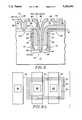
- FIGS. 1-8, 1A, 4A, 6A and 8Aare plan and sectional views of a semiconductor substrate at various stages of processing in accordance with the invention that ultimately form an insulated-gate vertical FET.
- a semiconductor substrate 12forms the starting material for the FET.
- the substrate materialcan be P-type or N-type silicon formed in a wafer, epitaxial layer, or well.
- the top surface of the substratedefines a reference surface for defining subsequent vertical structures.
- a trench in the substrate 12forms the channel region and the gate structure of the vertical FET 10.
- the trenchdefines a surface including first and second mesa portions 14A and 14B at the level of the reference surface of the substrate 12, one or more sidewalls 16, and a base 18 recessed from the reference surface.
- An insulated gate layer 20is formed on the sidewalls 16 of the trench, which includes a gate dielectric layer 22 and a gate conductive layer 24.
- a first enhanced N-type layer 26 implanted in the first portion of the mesa 14Aforms the first current node of the transistor, typically the drain. However, since the drain and source are interchangeable in an FET, the N-type layer 26 can also serve as the source.
- a second enhanced N-type layer 28is implanted in the base 18 of the trench to form the second current node of the transistor, typically the source. Again, given the interchangeability of the current nodes, the second enhanced N-type layer 28 can also serve as the drain.
- a spacer dielectric layer 30partially fills the base 18 of the trench and a conductive layer 32 is deposited along the sidewalls 16 of the trench over the insulated gate layer 20 extending from the spacer dielectric layer 30 to the reference surface of the substrate 12.
- the conductive layer 32forms part of a gate contact and is spaced apart from the enhanced N-type layer 28 by the spacer dielectric layer 30 to decrease the parasitic overlap capacitance between the gate and source of the FET.
- the conductive layer 32 and the spacer dielectric layer 30are opened to expose the second enhanced N-type layer 28.
- a field dielectric layer 34covers the entire surface of the FET 10, and is opened in three places to form drain, source, and gate contacts.
- the field dielectric layer 34is opened above the first enhanced N-type layer 26 to form a drain contact 36, which is covered with an interconnect line 42; above the second enhanced N-type layer 28 to form a source contact 38, which is covered with an interconnect line 44; and above the conductive layer 32 in the second portion l4B of the mesa to form a gate contact 40, which is covered with an interconnect line 46.
- FIG. 1there is shown a sectional view of a partially processed silicon substrate 12 having a patterned photoresist layer 11 over an optional thin grown oxide layer 15.
- the substratecan be either P-type or N-type material depending upon whether an N-channel or a P-channel FET is desired.
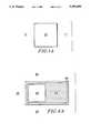
- FIG. IAis a corresponding plan view showing the contours of the photoresist opening, which will determine the nature of the trench.
- a trench having four sidewalls and a rectangular baseis formed.
- Other patterns, including a circular pattern resulting in one continuous sidewall and polygonal patterns result in multiple sidewallsare possible within the constraints of the photolithographic equipment that is used.
- the trenchis formed with a reactive ion etch, revealing first and second mesa portions 14A and 14B, sidewalls 16, and a base portion 18.
- the sidewalls 16 of the trenchform the body of the FET 10 that includes the channel region.
- the FET 10can thus be formed in one or more of the sidewalls 16.
- the etchant species for removing the silicon substrate and creating the trenchcan be CF 4 , or any other conventional etchant species.
- the depth of the trenchdefines the length of the channel of the FET 10. Therefore, the channel is ideally etched to a depth equal to the desired length of the channel region, up to a maximum length of about 8000 to 10000 Angstroms.
- the width, and consequently the width to length (“W/L”) ratio of the FET 10,is determined by the dimensions of the photoresist pattern.
- the insulated gate layer 20is revealed in greater detail.
- the insulated gate layer 20is comprised of a gate dielectric layer 22 such as oxide, and a gate conductive layer 24 such as polysilicon.
- the gate oxide layeris grown along the entire surface of the trench to a depth of about 200 to 250 Angstroms, but this depth can be made thinner or thicker as required by the application.
- the thin gate polysilicon layer 24is deposited onto the surface of the oxide layer 22 to a thickness of about 500 to 1000 Angstroms. Again, the thickness can be easily adjusted as required by the application.
- the gate polysilicon layer 24is highly conformal with oxide layer 22.
- the gate polysilicon layer 24forms the active gate contact of the FET 10, which inverts the substrate silicon 12 in the sidewalls 16 of the trench.
- the gate polysilicon layer 24be doped with an appropriate dopant such as phosphorous to form a conductive layer capable of inverting the entire channel region.
- a suitable sheet resistance for the gate polysilicon layer 24 after the doping step is completedis about 50 ohms per square.
- the insulated gate layer 24is removed in a first portion 14A of the mesa, and first and second enhanced N-type ("N+") layers 26 and 28 are implanted into the first portion 14A of the mesa and into the base of the trench 18 to form the active drain and source of the FET 10.
- the gate polysilicon layer 24is removed with a reactive ion etch.
- the gate polysilicon layerremains on the sidewalls 16 since the reactive ion etch acts primarily in the vertical directional and the gate polysilicon layer 24 is conformal to the sidewalls 16.
- the gate oxide layer 22is removed from the first portion 14A of the mesa and the base 18 by an oxide etch.
- first and second enhanced N-type layers 26 and 28are implanted into the first portion of the mesa 14A and the base 18.
- a suitable implant dosageis 9 ⁇ 10 15 ions per cm 2 at 30 KeV.
- the P-N junction between the enhanced N-type layers and the P-type body of the FET 10 using this implant dosageoccurs at a depth of approximately 2000 to 4000 Angstroms.
- FIG. 4AThe corresponding plan view is shown in FIG. 4A, revealing the first enhanced N-type layer 26 in the first portion of the mesa 14A, the gate dielectric layer 22 and the gate conductive layer 24 along the sidewalls of the trench and in the second portion of the mesa l4B, and the second enhanced N-type layer 28 in the base of the trench.
- the base 18 of the trenchis partially filled with a spacer oxide layer 30 in FIG. 5.
- the spacer oxide layer 30minimizes the parasitic overlap capacitance between the gate and the source of the FET 10.
- the spacer oxide layer 30is a thick conformal layer that is deposited over the surface of the FET 10, which completely fills in the trench.
- a mechanical planerizationremoves most of the spacer oxide layer 30 from the mesa portions of the trench, while leaving the spacer oxide layer 30 in the trench.
- a subsequent oxide etchremoves any remaining oxide from the mesa portions of the trench, and etches back the spacer oxide layer 30 in the trench to partially fill the trench to a thickness of about 2000 to 3000 Angstroms.
- the thickness of the spacer oxide layer 30can be adjusted depending upon the reduction in the parasitic overlap capacitance that is desired.
- a conductive layer 32is added that contacts the insulated gate layer 20 in order to provide a surface contact for the gate of the FET 10.
- the conductive layer 32is a conformal polysilicon layer that is deposited over the entire surface. Once the conductive layer 32 has been deposited, it is masked and etched away in the first portion 14A of the mesa and at the base 18 of the trench. The conductive layer remains on the sidewalls 16 of the trench and in the second portion 14B of the mesa.
- a suitable thickness for the conductive layeris about 2000 Angstroms.
- the polysiliconis doped with an appropriate dopant such as phosphorous to render it conductive.
- a suitable sheet resistance upon completion of the doping stepis about 25 to 35 ohms per square.
- FIG. 6AThe corresponding plan view is shown in FIG. 6A, revealing the first enhenced N-type layer 26 in the first portion of the mesa 14A, the gate dielectric layer 22, the gate conductive layer 24, and the conductive layer 32 along the sidewalls of the trench and in the second portion of the mesa 14B, and the spacer dielectric layer 30 in the base of the trench.
- a center portion of the spacer dielectric layer 30is etched away using a conventional oxide etch to reveal the second enhanced N-type layer 28.
- the opening in the spacer dielectric layer 30subsequently serves as a &op surface source contact.
- a thick, conformal field dielectric layer 34such as oxide is subsequently deposited over the entire surface of the FET 10.
- the field dielectricis etched in three places to form a drain contact 36, a source contact 38, and a gate contact 40.
- Each contactis respectively covered with a separate interconnect line 42, 44, and 46 for interconnecting the FET 10 with other circuit components.
- the interconnect linescan be polysilicon, doped polysilicon, or metal such as gold or aluminum.
- FIG. 8AThe corresponding plan view is shown in FIG. 8A in outline form only.
- the outline of the gate dielectric layer 22, the gate conductive layer 24, and the conductive layer 32 along the sidewalls of the trench and in the second portion of the mesa 14Bis shown.
- the location of the drain contact 36, source contact 38, and gate contact 40, as well as the drain interconnect line 42, the source interconnect line 44, and the gate interconnect lineis also shown.
- an insulated-gate vertical FEThas a small horizontal area suitable for high density integration on a silicon die, since the gate and channel area are disposed along and within one or more sidewalls of the trench.
- the active gate regionis continuous along the trench sidewall and is protected from further processing steps.
- the active gate region within each trench sidewall 16is continuous from the mesa to the base and contains no sharp corners, edges, steps or other such discontinuous features that decrease breakdown voltage.
- Low parasitic gate-to-source overlap capacitanceis reduced by the spacer dielectric layer 30 in order to maintain a high maximum operating frequency. Note in FIG. 8 that only the thin gate conductive layer 24 remains in close proximity to the second enhanced N-type layer 28, establishing a minimum overlap capacitance.
- the vertical FEThas a high current drive capability at a given W/L ratio since the parasitic capacitance is low. It has also been shown that the vertical FET 10 requires no additional masking steps beyond those normally required for the fabrication of an integrated random access memory. For example, the N+ implant used to form the source and drain regions is typically creates the storage node of the capacitor for a memory cell.
- the source, drain, and gate contacts of the vertical FET 10may all be contacted from the top surface of the die, if desired. It is appreciated, however, by those skilled in the art that the exact configuration and layout of the FET 10 can be changed in many ways. For example, the drain and gate contacts need not be placed in a row as shown in FIGS. 8 and 8A, but can be orthogonally arranged if required by layout considerations. Also, the source region of the FET 10 need not be contacted from the surface, but can be contacted through additional N-type layers in contact with N-type layer 28, or by directly metallizing the bottom surface of the die by any conventional means taught in the prior art. The source region of the FET 10 may also be coupled to a capacitor in a DRAM array configuration, while still maintaining the minimized gate-to-source overlap capacitance of the present invention.
- the vertical FET 10 of the present inventionis suitable for use in many applications, such as in a DRAM array, in an inverter, a buffer or driver circuit, or a stand-alone power FET. If minimum area is required, it is desirable that the gate of the vertical FET 10 be constructed in only one of the sidewalls of a rectangular trench. If maximum drive current is required for a power FET, it is desirable that the gate of the vertical FET 10 be constructed in all four sidewalls of a rectangular trench.
Landscapes
- Engineering & Computer Science (AREA)
- Manufacturing & Machinery (AREA)
- Insulated Gate Type Field-Effect Transistor (AREA)
Abstract
Description
This is a division, of application Ser. No. 07/682,623, filed Apr. 8, 1991, now U.S. Pat. No. 5122848
This invention relates generally to field-effect transistors ("FETs"), and more particularly to those FETs having a channel region that is generally vertical with respect to the horizontal plane of the silicon wafer.
As the performance and complexity of integrated circuits, and in particular memory circuits, increases, the area of an individual transistor on the integrated circuit must decrease in order to maintain die size and to control manufacturing costs. In the past, vertical FETs were introduced either in a trench or a V-groove to align the channel region of the FET vertically. Therefore, the area of the FET could be reduced because the channel did not use valuable horizontal area leading to a larger die area. A problem with many of the vertical designs is that performance is sacrificed as the area is decreased. Parasitic capacitance from the gate of the FET to the source ("overlap capacitance"), drain, or substrate can increase in the vertical FET, which results in a lower maximum operating frequency. In addition, in many vertical designs, the drain contact is made at the bottom of the FET through the substrate or by directly metallizing the bottom surface of the die, and thus the drain and source contacts cannot both be made at the surface of the transistor.
Accordingly, a need remains for a vertical FET having an area smaller than a horizontal FET having a comparable channel region, while having minimum gate parasitic capacitance and the option of surface gate, source, and drain contacts.
It is, therefore, an object of the invention to provide a vertical FET having a small horizontal area suitable for high density integration on a silicon die.
Another object of the invention is to provide a vertical FET having low parasitic gate capacitance in order to maintain a high maximum operating frequency.
A further object of the invention is to provide a vertical FET having a high current drive capability.
An advantage of the invention is that the vertical FET requires no additional masking steps beyond those normally required for the fabrication of an integrated random access memory.
Another advantage of the invention is that the source, drain, and gate contacts of the vertical FET may all be contacted from the top surface of the die, if desired.
Another advantage of the invention is that the gate region within each trench sidewall contains no discontinuous features that decrease breakdown voltage.
According to the present invention, an insulated-gate vertical FET has a channel region and gate structure that is formed along the sidewall of trench in a P-type semiconductor substrate. The drain and source regions of the FET are formed in the mesa and the base portions of the trench. All contacts to the gate, drain, and source regions can be made from the top surface of the semiconductor substrate. One or more sidewalls of the trench are oxidized with a thin gate oxide dielectric layer followed by a thin polysilicon deposited film to form an insulated gate layer. A reactive ion etch step removes the insulated gate layer from the mesa and the base portions of the trench. An enhanced N-type implant creates the drain and source regions in the mesa and the base portions of the trench. The trench is partially filled with a spacer oxide layer to reduce gate-to-source overlap capacitance. A conformal conductive polysilicon layer is deposited over the insulated gate layer. A portion of the conductive polysilicon layer is extended above the surface of the trench onto the mesa to form a gate contact. A field oxide covers the entire surface of the FET, which is opened in the mesa to form gate and drain contacts, and in the base to form the source contact.
The foregoing and other objects, features and advantages of the invention are more readily apparent from the following detailed description of a preferred embodiment of the invention, which proceeds with reference to the accompanying drawings.
FIGS. 1-8, 1A, 4A, 6A and 8A are plan and sectional views of a semiconductor substrate at various stages of processing in accordance with the invention that ultimately form an insulated-gate vertical FET.
The sectional view of a completed insulated-gatevertical FET 10 is shown in the sectional view of FIG. 8. Asemiconductor substrate 12 forms the starting material for the FET. The substrate material can be P-type or N-type silicon formed in a wafer, epitaxial layer, or well. The top surface of the substrate defines a reference surface for defining subsequent vertical structures. A trench in thesubstrate 12 forms the channel region and the gate structure of thevertical FET 10. The trench defines a surface including first andsecond mesa portions substrate 12, one ormore sidewalls 16, and abase 18 recessed from the reference surface. An insulatedgate layer 20 is formed on thesidewalls 16 of the trench, which includes a gatedielectric layer 22 and a gateconductive layer 24.
A first enhanced N-type layer 26 implanted in the first portion of themesa 14A forms the first current node of the transistor, typically the drain. However, since the drain and source are interchangeable in an FET, the N-type layer 26 can also serve as the source. A second enhanced N-type layer 28 is implanted in thebase 18 of the trench to form the second current node of the transistor, typically the source. Again, given the interchangeability of the current nodes, the second enhanced N-type layer 28 can also serve as the drain.
A spacerdielectric layer 30 partially fills thebase 18 of the trench and aconductive layer 32 is deposited along thesidewalls 16 of the trench over the insulatedgate layer 20 extending from the spacerdielectric layer 30 to the reference surface of thesubstrate 12. Theconductive layer 32 forms part of a gate contact and is spaced apart from the enhanced N-type layer 28 by the spacerdielectric layer 30 to decrease the parasitic overlap capacitance between the gate and source of the FET.
Theconductive layer 32 and the spacerdielectric layer 30 are opened to expose the second enhanced N-type layer 28. A fielddielectric layer 34 covers the entire surface of theFET 10, and is opened in three places to form drain, source, and gate contacts. The fielddielectric layer 34 is opened above the first enhanced N-type layer 26 to form adrain contact 36, which is covered with aninterconnect line 42; above the second enhanced N-type layer 28 to form asource contact 38, which is covered with aninterconnect line 44; and above theconductive layer 32 in the second portion l4B of the mesa to form agate contact 40, which is covered with aninterconnect line 46.
The structure and method for making theFET 10, and the nature of the individual layers including dimensions and suitable materials is described in greater detail below.
Referring now to FIG. 1, there is shown a sectional view of a partially processedsilicon substrate 12 having a patternedphotoresist layer 11 over an optional thin grownoxide layer 15. The substrate can be either P-type or N-type material depending upon whether an N-channel or a P-channel FET is desired. FIG. IA is a corresponding plan view showing the contours of the photoresist opening, which will determine the nature of the trench. In the case of a rectangular pattern, a trench having four sidewalls and a rectangular base is formed. Other patterns, including a circular pattern resulting in one continuous sidewall and polygonal patterns result in multiple sidewalls are possible within the constraints of the photolithographic equipment that is used.
In FIG. 2, the trench is formed with a reactive ion etch, revealing first andsecond mesa portions sidewalls 16, and abase portion 18. Thesidewalls 16 of the trench form the body of the FET 10 that includes the channel region. The FET 10 can thus be formed in one or more of thesidewalls 16. The etchant species for removing the silicon substrate and creating the trench can be CF4, or any other conventional etchant species. The depth of the trench defines the length of the channel of the FET 10. Therefore, the channel is ideally etched to a depth equal to the desired length of the channel region, up to a maximum length of about 8000 to 10000 Angstroms. The width, and consequently the width to length ("W/L") ratio of theFET 10, is determined by the dimensions of the photoresist pattern.
In FIG. 3, the insulatedgate layer 20 is revealed in greater detail. The insulatedgate layer 20 is comprised of a gatedielectric layer 22 such as oxide, and a gateconductive layer 24 such as polysilicon. The gate oxide layer is grown along the entire surface of the trench to a depth of about 200 to 250 Angstroms, but this depth can be made thinner or thicker as required by the application. The thingate polysilicon layer 24 is deposited onto the surface of theoxide layer 22 to a thickness of about 500 to 1000 Angstroms. Again, the thickness can be easily adjusted as required by the application. Thegate polysilicon layer 24 is highly conformal withoxide layer 22. Thegate polysilicon layer 24 forms the active gate contact of theFET 10, which inverts thesubstrate silicon 12 in thesidewalls 16 of the trench. Therefore, it is desirable that thegate polysilicon layer 24 be doped with an appropriate dopant such as phosphorous to form a conductive layer capable of inverting the entire channel region. A suitable sheet resistance for thegate polysilicon layer 24 after the doping step is completed is about 50 ohms per square.
In FIG. 4, theinsulated gate layer 24 is removed in afirst portion 14A of the mesa, and first and second enhanced N-type ("N+") layers 26 and 28 are implanted into thefirst portion 14A of the mesa and into the base of thetrench 18 to form the active drain and source of theFET 10. Thegate polysilicon layer 24 is removed with a reactive ion etch. The gate polysilicon layer remains on thesidewalls 16 since the reactive ion etch acts primarily in the vertical directional and thegate polysilicon layer 24 is conformal to thesidewalls 16. After thegate polysilicon layer 24 is removed with the reactive ion etch, thegate oxide layer 22 is removed from thefirst portion 14A of the mesa and the base 18 by an oxide etch. After theinsulated gate layer 20 is removed, first and second enhanced N-type layers mesa 14A and thebase 18. A suitable implant dosage is 9×10¹⁵ ions per cm2 at 30 KeV. The P-N junction between the enhanced N-type layers and the P-type body of theFET 10 using this implant dosage occurs at a depth of approximately 2000 to 4000 Angstroms.
The corresponding plan view is shown in FIG. 4A, revealing the first enhanced N-type layer 26 in the first portion of themesa 14A, thegate dielectric layer 22 and the gateconductive layer 24 along the sidewalls of the trench and in the second portion of the mesa l4B, and the second enhanced N-type layer 28 in the base of the trench.
Thebase 18 of the trench is partially filled with aspacer oxide layer 30 in FIG. 5. Thespacer oxide layer 30 minimizes the parasitic overlap capacitance between the gate and the source of theFET 10. Thespacer oxide layer 30 is a thick conformal layer that is deposited over the surface of theFET 10, which completely fills in the trench. A mechanical planerization removes most of thespacer oxide layer 30 from the mesa portions of the trench, while leaving thespacer oxide layer 30 in the trench. A subsequent oxide etch removes any remaining oxide from the mesa portions of the trench, and etches back thespacer oxide layer 30 in the trench to partially fill the trench to a thickness of about 2000 to 3000 Angstroms. However, the thickness of thespacer oxide layer 30 can be adjusted depending upon the reduction in the parasitic overlap capacitance that is desired.
In FIG. 6 aconductive layer 32 is added that contacts theinsulated gate layer 20 in order to provide a surface contact for the gate of theFET 10. Theconductive layer 32 is a conformal polysilicon layer that is deposited over the entire surface. Once theconductive layer 32 has been deposited, it is masked and etched away in thefirst portion 14A of the mesa and at thebase 18 of the trench. The conductive layer remains on thesidewalls 16 of the trench and in thesecond portion 14B of the mesa. A suitable thickness for the conductive layer is about 2000 Angstroms. The polysilicon is doped with an appropriate dopant such as phosphorous to render it conductive. A suitable sheet resistance upon completion of the doping step is about 25 to 35 ohms per square.
The corresponding plan view is shown in FIG. 6A, revealing the first enhenced N-type layer 26 in the first portion of themesa 14A, thegate dielectric layer 22, the gateconductive layer 24, and theconductive layer 32 along the sidewalls of the trench and in the second portion of themesa 14B, and thespacer dielectric layer 30 in the base of the trench.
In FIG. 7, a center portion of thespacer dielectric layer 30 is etched away using a conventional oxide etch to reveal the second enhanced N-type layer 28. The opening in thespacer dielectric layer 30 subsequently serves as a &op surface source contact. A thick, conformalfield dielectric layer 34 such as oxide is subsequently deposited over the entire surface of theFET 10. As discussed above, the field dielectric is etched in three places to form adrain contact 36, asource contact 38, and agate contact 40. Each contact is respectively covered with aseparate interconnect line FET 10 with other circuit components. The interconnect lines can be polysilicon, doped polysilicon, or metal such as gold or aluminum.
The corresponding plan view is shown in FIG. 8A in outline form only. The outline of thegate dielectric layer 22, the gateconductive layer 24, and theconductive layer 32 along the sidewalls of the trench and in the second portion of themesa 14B is shown. The location of thedrain contact 36,source contact 38, andgate contact 40, as well as thedrain interconnect line 42, thesource interconnect line 44, and the gate interconnect line is also shown.
Therefore, it has been shown that an insulated-gate vertical FET has a small horizontal area suitable for high density integration on a silicon die, since the gate and channel area are disposed along and within one or more sidewalls of the trench. The active gate region is continuous along the trench sidewall and is protected from further processing steps. The active gate region within eachtrench sidewall 16 is continuous from the mesa to the base and contains no sharp corners, edges, steps or other such discontinuous features that decrease breakdown voltage. Low parasitic gate-to-source overlap capacitance is reduced by thespacer dielectric layer 30 in order to maintain a high maximum operating frequency. Note in FIG. 8 that only the thin gateconductive layer 24 remains in close proximity to the second enhanced N-type layer 28, establishing a minimum overlap capacitance. Furthermore, the vertical FET has a high current drive capability at a given W/L ratio since the parasitic capacitance is low. It has also been shown that thevertical FET 10 requires no additional masking steps beyond those normally required for the fabrication of an integrated random access memory. For example, the N+ implant used to form the source and drain regions is typically creates the storage node of the capacitor for a memory cell.
It has also been shown that the source, drain, and gate contacts of thevertical FET 10 may all be contacted from the top surface of the die, if desired. It is appreciated, however, by those skilled in the art that the exact configuration and layout of theFET 10 can be changed in many ways. For example, the drain and gate contacts need not be placed in a row as shown in FIGS. 8 and 8A, but can be orthogonally arranged if required by layout considerations. Also, the source region of theFET 10 need not be contacted from the surface, but can be contacted through additional N-type layers in contact with N-type layer 28, or by directly metallizing the bottom surface of the die by any conventional means taught in the prior art. The source region of theFET 10 may also be coupled to a capacitor in a DRAM array configuration, while still maintaining the minimized gate-to-source overlap capacitance of the present invention.
Thevertical FET 10 of the present invention is suitable for use in many applications, such as in a DRAM array, in an inverter, a buffer or driver circuit, or a stand-alone power FET. If minimum area is required, it is desirable that the gate of thevertical FET 10 be constructed in only one of the sidewalls of a rectangular trench. If maximum drive current is required for a power FET, it is desirable that the gate of thevertical FET 10 be constructed in all four sidewalls of a rectangular trench.
Having described and illustrated the principles of the invention in a preferred embodiment thereof, it is apparent that the invention can be modified in arrangement and detail without departing from those principles. For example, the polarity of the N-type and P-type layers discussed herein can be reversed, depending upon whether a P-channel or N-channel device is selected. As another example, the materials selected for the various layers and their attendant specifications can all be changed to suit the requirements of the application. Therefore, we claim all modifications and variations of the invention falling within the spirit and scope of the following claims.
Claims (19)
1. A method of fabricating an insulated-gate vertical field-effect transistor comprising the steps of:
a) providing a semiconductor substrate of a first conductivity type having a reference surface;
b) forming a trench in the semiconductor substrate, the trench defining a surface including a mesa at the level of the reference surface, a sidewall, and a base recessed from the reference surface;
c) forming an insulated gate layer on the sidewall;
d) forming a first layer of a second conductivity type in the mesa and a second layer of the second conductivity type in the base of the trench;
e) partially filling the trench with a spacer dielectric layer, by:
depositing a spacer dielectric layer atop the surface of the trench;
planarizing the spacer dielectric layer on the mesa of the trench; and
etching the spacer dielectric layer in the base of the trench to a predetermined thickness;
f) forming a conductive layer along the sidewall of the trench over the insulated gate layer extending from the spacer dielectric layer to the reference surface; and
g) the conductive layer being spaced apart from the second layer of the second conductivity type by the spacer dielectric layer to decrease a parasitic capacitance between the conductive layer and the second layer of the second conductivity type.
2. A method according to claim 1 including the step of sizing the thickness of the spacer dielectric layer to decrease the parasitic capacitance below a predetermined capacitance.
3. A method according to claim 2 in which the step of sizing the thickness of the spacer dielectric comprises etching the spacer dielectric to a predetermined thickness.
4. A method according to claim 1 in which the step of forming an insulated gate layer on the sidewall comprises the steps of:
forming a gate dielectric layer on the surface of the trench;
forming a gate conductive layer atop the gate dielectric layer; and
selectively removing the gate dielectric layer and the gate conductive layer from the mesa and the base of the trench.
5. A method according to claim 1 in which the step of forming the first layer of the second conductivity type in the mesa comprises forming the first layer of the second conductivity type in a first portion of the mesa.
6. A method according to claim 5 comprising the steps of:
extending the insulated gate layer above the reference surface and onto a second portion of the mesa; and extending the conductive layer above the reference surface and onto the insulated gate layer on the second portion of the mesa.
7. A method according to claim 6 comprising the steps of:
forming a field dielectric layer covering the conductive layer on the second portion of the mesa;
opening the field dielectric layer covering the conductive layer on the second portion of the mesa to form a gate contact; and
covering the gate contact with an interconnect line.
8. A method according to claim 5 comprising the steps of:
forming a field dielectric layer covering first layer of the second conductivity type on the first portion of the mesa;
opening the field dielectric layer above the first layer of the second conductivity type on the first portion of the mesa to form a first current node contact; and
covering the first current node contact with an interconnect line.
9. A method of fabricating an insulated-gate vertical field-effect transistor comprising the steps of:
a) providing a semiconductor substrate of a first conductivity type having a reference surface;
b) forming a trench in the semiconductor substrate, the trench defining a surface including a mesa at the level of the reference surface, a sidewall, and a base recessed from the reference surface;
c) forming an insulated gate layer on the sidewall;
d) forming a first layer of a second conductivity type in the mesa and a second layer of the second conductivity type in the base of the trench;
e) forming a conductor that extends from the mesa of the trench to the base of the trench to ohmically contact the second layer of the second conductivity type;
f) partially filling the trench with a spacer dielectric layer; and
g) opening the spacer dielectric layer to expose the layer of the second conductivity type at the base of the trench for ohmic contact with the conductor.
10. A method according to claim 9 in which the step of forming a conductor comprises forming a conductor that is electrically insulated from the insulated gate layer and from the first layer of the second conductivity type.
11. A method according to claim 9 in which the step of forming an insulated gate layer on the sidewall comprises the steps of:
forming a gate dielectric layer on the surface of the trench;
forming a gate conductive layer atop the gate dielectric layer; and
selectively removing the gate dielectric layer and the conductive layer from the mesa and the base of the trench.
12. A method according to claim 9 in which the step of partially filling the trench comprises the steps of:
depositing a spacer dielectric layer atop the surface of the trench;
planarizing the spacer dielectric layer on the mesa of the trench; and
etching the spacer dielectric layer in the base of the trench to a predetermined thickness.
13. A method according to claim 9 including the step of forming a conductive layer along the sidewall of the trench over the insulated gate layer extending from the spacer oxide layer to the reference surface.
14. A method according to claim 9 comprising the steps of:
opening the spacer dielectric layer to expose the layer of the second conductivity type at the base of the trench;
forming a field dielectric layer covering the second layer the second conductivity type in the base of the trench;
opening the field dielectric layer above the second layer of the second conductivity type to form a second current node contact; and
ohmically contacting the second current node contact with the conductor.
15. A method according to claim 9 in which the step of forming the first layer of the second conductivity type in the mesa comprises forming the first layer of the second conductivity type in a first portion of the mesa.
16. A method according to claim 15 comprising the steps of:
extending the insulated gate layer above the reference surface and onto a second portion of the mesa; and
extending the conductive layer above the reference surface and onto the insulated gate layer on the second portion of the mesa.
17. A method according to claim 16 comprising the steps of:
forming a field dielectric layer covering the conductive layer on the second portion of the mesa;
opening the field dielectric layer above the conductive layer on the second portion of the mesa to form a gate contact; and
covering the gate contact with an interconnect line.
18. A method according to claim 15 comprising the steps of:
forming a field dielectric layer covering the first layer of the second conductivity type on the first portion of the mesa;
opening the field dielectric layer above the first layer of the second conductivity type on the first portion of the mesa to form a first current mode contact; and
covering the first current node contact with an interconnect line.
19. A method of fabricating an insulated-gate vertical field-effect transistor comprising the steps of:
a) providing a semiconductor substrate of a first condustivity type having a reference surface;
b) forming a trench in the semiconductor substrate, the trench defining a surface including a mesa at the level of the reference surface, a sidewall, and a base recessed from the reference surface;
c) forming an insulated gate layer on the sidewall;
d) forming a first layer of a second conductivity type in the mesa and a second layer of the second conductivity type in the base of the trench;
e) partially filling the trench with a spacer dielectric layer;
f) forming a conductive layer along the sidewall of the trench over the insulated gate layer extending from the spacer dielectric layer to the reference surface;
g) the conductive layer being spaced apart from the second layer of the second conductivity type by the spacer dielectric layer to decrease a parasitic capacitance between the conductive layer and the second layer of the second conductivity type;
h) opening the spacer dielectric layer to expose the layer of the second conductivity type at the base of the trench; and
i) forming a field dielectric layer covering the second layer of the second conductivity type in the base of the trench;
j) opening the field dielectric layer above the second layer of the second conductivity type to form a second current node contact; and
k) covering the second current node contact with an interconnect line.
Priority Applications (1)
| Application Number | Priority Date | Filing Date | Title |
|---|---|---|---|
| US07/835,691US5250450A (en) | 1991-04-08 | 1992-02-12 | Insulated-gate vertical field-effect transistor with high current drive and minimum overlap capacitance |
Applications Claiming Priority (2)
| Application Number | Priority Date | Filing Date | Title |
|---|---|---|---|
| US07/682,623US5122848A (en) | 1991-04-08 | 1991-04-08 | Insulated-gate vertical field-effect transistor with high current drive and minimum overlap capacitance |
| US07/835,691US5250450A (en) | 1991-04-08 | 1992-02-12 | Insulated-gate vertical field-effect transistor with high current drive and minimum overlap capacitance |
Related Parent Applications (1)
| Application Number | Title | Priority Date | Filing Date |
|---|---|---|---|
| US07/682,623DivisionUS5122848A (en) | 1991-04-08 | 1991-04-08 | Insulated-gate vertical field-effect transistor with high current drive and minimum overlap capacitance |
Publications (1)
| Publication Number | Publication Date |
|---|---|
| US5250450Atrue US5250450A (en) | 1993-10-05 |
Family
ID=27102930
Family Applications (1)
| Application Number | Title | Priority Date | Filing Date |
|---|---|---|---|
| US07/835,691Expired - LifetimeUS5250450A (en) | 1991-04-08 | 1992-02-12 | Insulated-gate vertical field-effect transistor with high current drive and minimum overlap capacitance |
Country Status (1)
| Country | Link |
|---|---|
| US (1) | US5250450A (en) |
Cited By (74)
| Publication number | Priority date | Publication date | Assignee | Title |
|---|---|---|---|---|
| US5312767A (en)* | 1989-12-15 | 1994-05-17 | Mitsubishi Denki Kabushiki Kaisha | MOS type field effect transistor and manufacturing method thereof |
| US5391505A (en)* | 1993-11-01 | 1995-02-21 | Lsi Logic Corporation | Active device constructed in opening formed in insulation layer and process for making same |
| US5407846A (en)* | 1992-07-01 | 1995-04-18 | Chan, Ha Hyoung | Method of manufacturing a thin film transistor |
| US5424231A (en)* | 1994-08-09 | 1995-06-13 | United Microelectronics Corp. | Method for manufacturing a VDMOS transistor |
| US5460987A (en)* | 1994-12-27 | 1995-10-24 | United Microelectronics Corporation | Method of making field effect transistor structure of a diving channel device |
| US5480820A (en)* | 1993-03-29 | 1996-01-02 | Motorola, Inc. | Method of making a vertically formed neuron transistor having a floating gate and a control gate and a method of formation |
| AU684819B2 (en)* | 1993-08-19 | 1998-01-08 | Janssen Pharmaceutica N.V. | Vasoconstrictive substituted dihydropyranopyridines |
| US5714786A (en)* | 1996-10-31 | 1998-02-03 | Micron Technology, Inc. | Transistors having controlled conductive spacers, uses of such transistors and methods of making such transistors |
| US5719067A (en)* | 1996-09-06 | 1998-02-17 | Advanced Micro Devices, Inc. | Trench transistor and method for making same |
| US5895253A (en)* | 1997-08-22 | 1999-04-20 | Micron Technology, Inc. | Trench isolation for CMOS devices |
| US5933717A (en)* | 1997-03-04 | 1999-08-03 | Advanced Micro Devices, Inc. | Vertical transistor interconnect structure and fabrication method thereof |
| US5940707A (en)* | 1996-10-08 | 1999-08-17 | Advanced Micro Devices, Inc. | Vertically integrated advanced transistor formation |
| US5967030A (en)* | 1995-11-17 | 1999-10-19 | Micron Technology, Inc. | Global planarization method and apparatus |
| US6049496A (en)* | 1998-03-30 | 2000-04-11 | Micron Technology, Inc. | Circuit and method for low voltage, current sense amplifier |
| US6060754A (en)* | 1998-03-30 | 2000-05-09 | Micron Technology, Inc. | Circuit and method for gate-body structures in CMOS technology |
| US6069384A (en)* | 1997-03-04 | 2000-05-30 | Advanced Micro Devices, Inc. | Integrated circuit including vertical transistors with spacer gates having selected gate widths |
| US6075272A (en)* | 1998-03-30 | 2000-06-13 | Micron Technology, Inc. | Structure for gated lateral bipolar transistors |
| US6097065A (en)* | 1998-03-30 | 2000-08-01 | Micron Technology, Inc. | Circuits and methods for dual-gated transistors |
| US6104066A (en)* | 1998-03-30 | 2000-08-15 | Micron Technology, Inc. | Circuit and method for low voltage, voltage sense amplifier |
| US6177333B1 (en) | 1999-01-14 | 2001-01-23 | Micron Technology, Inc. | Method for making a trench isolation for semiconductor devices |
| US6180958B1 (en)* | 1997-02-07 | 2001-01-30 | James Albert Cooper, Jr. | Structure for increasing the maximum voltage of silicon carbide power transistors |
| US6218316B1 (en) | 1998-10-22 | 2001-04-17 | Micron Technology, Inc. | Planarization of non-planar surfaces in device fabrication |
| US6229342B1 (en) | 1998-03-30 | 2001-05-08 | Micron Technology, Inc. | Circuits and method for body contacted and backgated transistors |
| US6268249B1 (en)* | 1998-09-14 | 2001-07-31 | Hyundai Electronics Industries Co., Ltd. | Semiconductor device and method of fabricating the same |
| US6307235B1 (en) | 1998-03-30 | 2001-10-23 | Micron Technology, Inc. | Another technique for gated lateral bipolar transistors |
| US6316363B1 (en) | 1999-09-02 | 2001-11-13 | Micron Technology, Inc. | Deadhesion method and mechanism for wafer processing |
| US6331488B1 (en) | 1997-05-23 | 2001-12-18 | Micron Technology, Inc. | Planarization process for semiconductor substrates |
| US6448615B1 (en) | 1998-02-26 | 2002-09-10 | Micron Technology, Inc. | Methods, structures, and circuits for transistors with gate-to-body capacitive coupling |
| US6461918B1 (en) | 1999-12-20 | 2002-10-08 | Fairchild Semiconductor Corporation | Power MOS device with improved gate charge performance |
| US6489652B1 (en)* | 1995-11-11 | 2002-12-03 | Fairchild Semiconductor Corporation | Trench DMOS device having a high breakdown resistance |
| US6518172B1 (en) | 2000-08-29 | 2003-02-11 | Micron Technology, Inc. | Method for applying uniform pressurized film across wafer |
| US6570185B1 (en)* | 1997-02-07 | 2003-05-27 | Purdue Research Foundation | Structure to reduce the on-resistance of power transistors |
| US6570207B2 (en) | 2000-12-13 | 2003-05-27 | International Business Machines Corporation | Structure and method for creating vertical capacitor and anti-fuse in DRAM process employing vertical array device cell complex |
| US6569738B2 (en)* | 2001-07-03 | 2003-05-27 | Siliconix, Inc. | Process for manufacturing trench gated MOSFET having drain/drift region |
| US6573136B1 (en)* | 2002-05-30 | 2003-06-03 | Infineon Technologies Ag | Isolating a vertical gate contact structure |
| US20030146470A1 (en)* | 2001-12-08 | 2003-08-07 | Koninklijke Philips Electronics N.V. | Trenched semiconductor devices and their manufacture |
| US20030164527A1 (en)* | 2002-01-16 | 2003-09-04 | Fuji Electric Co., Ltd. | Semiconductor device and its manufacturing method |
| US20040227182A1 (en)* | 2001-07-03 | 2004-11-18 | Siliconix Incorporated | Process for manufacturing trench MIS device having implanted drain-drift region and thick botton oxide |
| US20060052788A1 (en)* | 2003-02-04 | 2006-03-09 | Thelen Sarah L | Expandable fixation devices for minimally invasive surgery |
| US7078296B2 (en) | 2002-01-16 | 2006-07-18 | Fairchild Semiconductor Corporation | Self-aligned trench MOSFETs and methods for making the same |
| US7265415B2 (en) | 2004-10-08 | 2007-09-04 | Fairchild Semiconductor Corporation | MOS-gated transistor with reduced miller capacitance |
| US7265416B2 (en) | 2002-02-23 | 2007-09-04 | Fairchild Korea Semiconductor Ltd. | High breakdown voltage low on-resistance lateral DMOS transistor |
| US7319256B1 (en) | 2006-06-19 | 2008-01-15 | Fairchild Semiconductor Corporation | Shielded gate trench FET with the shield and gate electrodes being connected together |
| US7345342B2 (en) | 2001-01-30 | 2008-03-18 | Fairchild Semiconductor Corporation | Power semiconductor devices and methods of manufacture |
| US7352036B2 (en) | 2004-08-03 | 2008-04-01 | Fairchild Semiconductor Corporation | Semiconductor power device having a top-side drain using a sinker trench |
| US7368777B2 (en) | 2003-12-30 | 2008-05-06 | Fairchild Semiconductor Corporation | Accumulation device with charge balance structure and method of forming the same |
| US7385248B2 (en) | 2005-08-09 | 2008-06-10 | Fairchild Semiconductor Corporation | Shielded gate field effect transistor with improved inter-poly dielectric |
| US20080173920A1 (en)* | 2007-01-22 | 2008-07-24 | Micron Technology, Inc. | Memory having a vertical access device |
| US7429523B2 (en) | 2001-10-17 | 2008-09-30 | Fairchild Semiconductor Corporation | Method of forming schottky diode with charge balance structure |
| US7504306B2 (en) | 2005-04-06 | 2009-03-17 | Fairchild Semiconductor Corporation | Method of forming trench gate field effect transistor with recessed mesas |
| US7557032B2 (en) | 2005-09-01 | 2009-07-07 | Micron Technology, Inc. | Silicided recessed silicon |
| US7576388B1 (en) | 2002-10-03 | 2009-08-18 | Fairchild Semiconductor Corporation | Trench-gate LDMOS structures |
| US7582519B2 (en) | 2002-11-05 | 2009-09-01 | Fairchild Semiconductor Corporation | Method of forming a trench structure having one or more diodes embedded therein adjacent a PN junction |
| US7638841B2 (en) | 2003-05-20 | 2009-12-29 | Fairchild Semiconductor Corporation | Power semiconductor devices and methods of manufacture |
| US7713822B2 (en) | 2006-03-24 | 2010-05-11 | Fairchild Semiconductor Corporation | Method of forming high density trench FET with integrated Schottky diode |
| US7772668B2 (en) | 2007-12-26 | 2010-08-10 | Fairchild Semiconductor Corporation | Shielded gate trench FET with multiple channels |
| US7935999B2 (en) | 2005-09-01 | 2011-05-03 | Micron Technology, Inc. | Memory device |
| US7939409B2 (en) | 2005-09-01 | 2011-05-10 | Micron Technology, Inc. | Peripheral gate stacks and recessed array gates |
| US20110260288A1 (en)* | 2010-04-21 | 2011-10-27 | Elpida Memory, Inc. | Semiconductor device and method for manufacturing the same |
| US8222105B2 (en) | 2005-08-31 | 2012-07-17 | Micron Technology, Inc. | Methods of fabricating a memory device |
| US8319290B2 (en) | 2010-06-18 | 2012-11-27 | Fairchild Semiconductor Corporation | Trench MOS barrier schottky rectifier with a planar surface using CMP techniques |
| US20130075801A1 (en)* | 2011-09-23 | 2013-03-28 | Infineon Technologies Austria Ag | Self-adjusted capacitive structure |
| US8963212B2 (en) | 2008-12-08 | 2015-02-24 | Fairchild Semiconductor Corporation | Trench-based power semiconductor devices with increased breakdown voltage characteristics |
| US9425788B1 (en) | 2015-03-18 | 2016-08-23 | Infineon Technologies Austria Ag | Current sensors and methods of improving accuracy thereof |
| US9437503B1 (en) | 2015-12-22 | 2016-09-06 | International Business Machines Corporation | Vertical FETs with variable bottom spacer recess |
| US20170229558A1 (en)* | 2016-02-08 | 2017-08-10 | International Business Machines Corporation | Vertical transistor device |
| US9755071B1 (en) | 2016-06-30 | 2017-09-05 | International Business Machines Corporation | Merged gate for vertical transistors |
| US9853028B1 (en) | 2017-04-17 | 2017-12-26 | International Business Machines Corporation | Vertical FET with reduced parasitic capacitance |
| WO2018182699A1 (en)* | 2017-03-31 | 2018-10-04 | Intel Corporation | Vertical field effect transistors (vfets) with self-aligned wordlines |
| US10468524B2 (en) | 2017-03-24 | 2019-11-05 | International Business Machines Corporation | Vertical field effect transistor with improved reliability |
| US10515801B2 (en) | 2007-06-04 | 2019-12-24 | Micron Technology, Inc. | Pitch multiplication using self-assembling materials |
| US10566444B2 (en) | 2017-12-21 | 2020-02-18 | International Business Machines Corporation | Vertical fin field effect transistor with a reduced gate-to-bottom source/drain parasitic capacitance |
| US10672887B2 (en) | 2017-12-12 | 2020-06-02 | International Business Machines Corporation | Vertical FET with shaped spacer to reduce parasitic capacitance |
| US11404412B2 (en) | 2020-08-07 | 2022-08-02 | Samsung Electronics Co., Ltd. | Semiconductor device |
Citations (21)
| Publication number | Priority date | Publication date | Assignee | Title |
|---|---|---|---|---|
| US4116720A (en)* | 1977-12-27 | 1978-09-26 | Burroughs Corporation | Method of making a V-MOS field effect transistor for a dynamic memory cell having improved capacitance |
| US4199774A (en)* | 1978-09-18 | 1980-04-22 | The Board Of Trustees Of The Leland Stanford Junior University | Monolithic semiconductor switching device |
| US4272302A (en)* | 1979-09-05 | 1981-06-09 | The United States Of America As Represented By The Administrator Of The National Aeronautics And Space Administration | Method of making V-MOS field effect transistors utilizing a two-step anisotropic etching and ion implantation |
| JPS5758671A (en)* | 1980-09-25 | 1982-04-08 | Ishihara Sangyo Kaisha Ltd | Phenoxyalkylazole type compound and agricultural and gardening fungicide comprising it |
| US4359816A (en)* | 1980-07-08 | 1982-11-23 | International Business Machines Corporation | Self-aligned metal process for field effect transistor integrated circuits |
| US4364074A (en)* | 1980-06-12 | 1982-12-14 | International Business Machines Corporation | V-MOS Device with self-aligned multiple electrodes |
| US4364073A (en)* | 1980-03-25 | 1982-12-14 | Rca Corporation | Power MOSFET with an anode region |
| US4374455A (en)* | 1979-10-30 | 1983-02-22 | Rca Corporation | Method for manufacturing a vertical, grooved MOSFET |
| US4464212A (en)* | 1982-12-13 | 1984-08-07 | International Business Machines Corporation | Method for making high sheet resistivity resistors |
| US4476622A (en)* | 1981-12-24 | 1984-10-16 | Gte Laboratories Inc. | Recessed gate static induction transistor fabrication |
| US4503598A (en)* | 1982-05-20 | 1985-03-12 | Fairchild Camera & Instrument Corporation | Method of fabricating power MOSFET structure utilizing self-aligned diffusion and etching techniques |
| US4543706A (en)* | 1984-02-24 | 1985-10-01 | Gte Laboratories Incorporated | Fabrication of junction field effect transistor with filled grooves |
| US4566172A (en)* | 1984-02-24 | 1986-01-28 | Gte Laboratories Incorporated | Method of fabricating a static induction type recessed junction field effect transistor |
| US4567641A (en)* | 1982-04-12 | 1986-02-04 | General Electric Company | Method of fabricating semiconductor devices having a diffused region of reduced length |
| US4650544A (en)* | 1985-04-19 | 1987-03-17 | Advanced Micro Devices, Inc. | Shallow groove capacitor fabrication method |
| US4683643A (en)* | 1984-07-16 | 1987-08-04 | Nippon Telegraph And Telephone Corporation | Method of manufacturing a vertical MOSFET with single surface electrodes |
| US4689871A (en)* | 1985-09-24 | 1987-09-01 | Texas Instruments Incorporated | Method of forming vertically integrated current source |
| US4758528A (en)* | 1980-07-08 | 1988-07-19 | International Business Machines Corporation | Self-aligned metal process for integrated circuit metallization |
| US4859622A (en)* | 1986-11-12 | 1989-08-22 | Matsubishi Denki Kabushiki Kaisha | Method of making a trench capacitor for dram |
| US4920065A (en)* | 1988-10-31 | 1990-04-24 | International Business Machines Corporation | Method of making ultra dense dram cells |
| WO1990011615A1 (en)* | 1989-03-21 | 1990-10-04 | Grumman Aerospace Corporation | Trench gate metal oxide semiconductor transistor |
- 1992
- 1992-02-12USUS07/835,691patent/US5250450A/ennot_activeExpired - Lifetime
Patent Citations (21)
| Publication number | Priority date | Publication date | Assignee | Title |
|---|---|---|---|---|
| US4116720A (en)* | 1977-12-27 | 1978-09-26 | Burroughs Corporation | Method of making a V-MOS field effect transistor for a dynamic memory cell having improved capacitance |
| US4199774A (en)* | 1978-09-18 | 1980-04-22 | The Board Of Trustees Of The Leland Stanford Junior University | Monolithic semiconductor switching device |
| US4272302A (en)* | 1979-09-05 | 1981-06-09 | The United States Of America As Represented By The Administrator Of The National Aeronautics And Space Administration | Method of making V-MOS field effect transistors utilizing a two-step anisotropic etching and ion implantation |
| US4374455A (en)* | 1979-10-30 | 1983-02-22 | Rca Corporation | Method for manufacturing a vertical, grooved MOSFET |
| US4364073A (en)* | 1980-03-25 | 1982-12-14 | Rca Corporation | Power MOSFET with an anode region |
| US4364074A (en)* | 1980-06-12 | 1982-12-14 | International Business Machines Corporation | V-MOS Device with self-aligned multiple electrodes |
| US4359816A (en)* | 1980-07-08 | 1982-11-23 | International Business Machines Corporation | Self-aligned metal process for field effect transistor integrated circuits |
| US4758528A (en)* | 1980-07-08 | 1988-07-19 | International Business Machines Corporation | Self-aligned metal process for integrated circuit metallization |
| JPS5758671A (en)* | 1980-09-25 | 1982-04-08 | Ishihara Sangyo Kaisha Ltd | Phenoxyalkylazole type compound and agricultural and gardening fungicide comprising it |
| US4476622A (en)* | 1981-12-24 | 1984-10-16 | Gte Laboratories Inc. | Recessed gate static induction transistor fabrication |
| US4567641A (en)* | 1982-04-12 | 1986-02-04 | General Electric Company | Method of fabricating semiconductor devices having a diffused region of reduced length |
| US4503598A (en)* | 1982-05-20 | 1985-03-12 | Fairchild Camera & Instrument Corporation | Method of fabricating power MOSFET structure utilizing self-aligned diffusion and etching techniques |
| US4464212A (en)* | 1982-12-13 | 1984-08-07 | International Business Machines Corporation | Method for making high sheet resistivity resistors |
| US4566172A (en)* | 1984-02-24 | 1986-01-28 | Gte Laboratories Incorporated | Method of fabricating a static induction type recessed junction field effect transistor |
| US4543706A (en)* | 1984-02-24 | 1985-10-01 | Gte Laboratories Incorporated | Fabrication of junction field effect transistor with filled grooves |
| US4683643A (en)* | 1984-07-16 | 1987-08-04 | Nippon Telegraph And Telephone Corporation | Method of manufacturing a vertical MOSFET with single surface electrodes |
| US4650544A (en)* | 1985-04-19 | 1987-03-17 | Advanced Micro Devices, Inc. | Shallow groove capacitor fabrication method |
| US4689871A (en)* | 1985-09-24 | 1987-09-01 | Texas Instruments Incorporated | Method of forming vertically integrated current source |
| US4859622A (en)* | 1986-11-12 | 1989-08-22 | Matsubishi Denki Kabushiki Kaisha | Method of making a trench capacitor for dram |
| US4920065A (en)* | 1988-10-31 | 1990-04-24 | International Business Machines Corporation | Method of making ultra dense dram cells |
| WO1990011615A1 (en)* | 1989-03-21 | 1990-10-04 | Grumman Aerospace Corporation | Trench gate metal oxide semiconductor transistor |
Non-Patent Citations (6)
| Title |
|---|
| Krishna Shenai, A 55 V, 0.2 m . cm 2 Vertical Trench Power MOSFET, IEEE Electron Device Letters, vol. 12 No. 3, Mar. 1991, pp. 108 110.* |
| Krishna Shenai, A 55-V, 0.2-mΩ. cm2 Vertical Trench Power MOSFET, IEEE Electron Device Letters, vol. 12 No. 3, Mar. 1991, pp. 108-110. |
| Nicky C. C. Lu, Advanced Cell Structures for Dynamic RAMs, IEEE Circuits and Devices Magazine, Jan. 1989, pp. 27 36.* |
| Nicky C. C. Lu, Advanced Cell Structures for Dynamic RAMs, IEEE Circuits and Devices Magazine, Jan. 1989, pp. 27-36. |
| Tadahiro Ohmi, Power Static Induction Transistor Technology, IEEE Paper, Catalog No. CH1504 0/79/0000 0084 pp. 84 87 (1979).* |
| Tadahiro Ohmi, Power Static Induction Transistor Technology, IEEE Paper, Catalog No. CH1504-0/79/0000-0084 pp. 84-87 (1979). |
Cited By (166)
| Publication number | Priority date | Publication date | Assignee | Title |
|---|---|---|---|---|
| US5312767A (en)* | 1989-12-15 | 1994-05-17 | Mitsubishi Denki Kabushiki Kaisha | MOS type field effect transistor and manufacturing method thereof |
| US5508531A (en)* | 1992-07-01 | 1996-04-16 | Hyundai Electronics Industries Co., Ltd. | Thin film transistor (TFT) and method of manufacturing thereof |
| US5407846A (en)* | 1992-07-01 | 1995-04-18 | Chan, Ha Hyoung | Method of manufacturing a thin film transistor |
| US5583360A (en)* | 1993-03-29 | 1996-12-10 | Motorola Inc. | Vertically formed neuron transister having a floating gate and a control gate |
| US5480820A (en)* | 1993-03-29 | 1996-01-02 | Motorola, Inc. | Method of making a vertically formed neuron transistor having a floating gate and a control gate and a method of formation |
| AU684819B2 (en)* | 1993-08-19 | 1998-01-08 | Janssen Pharmaceutica N.V. | Vasoconstrictive substituted dihydropyranopyridines |
| US5391505A (en)* | 1993-11-01 | 1995-02-21 | Lsi Logic Corporation | Active device constructed in opening formed in insulation layer and process for making same |
| US5523600A (en)* | 1993-11-01 | 1996-06-04 | Lsi Logic Corporation | Active device constructed in opening formed in insulation layer |
| US5424231A (en)* | 1994-08-09 | 1995-06-13 | United Microelectronics Corp. | Method for manufacturing a VDMOS transistor |
| US5460987A (en)* | 1994-12-27 | 1995-10-24 | United Microelectronics Corporation | Method of making field effect transistor structure of a diving channel device |
| US6489652B1 (en)* | 1995-11-11 | 2002-12-03 | Fairchild Semiconductor Corporation | Trench DMOS device having a high breakdown resistance |
| US5967030A (en)* | 1995-11-17 | 1999-10-19 | Micron Technology, Inc. | Global planarization method and apparatus |
| US6237483B1 (en) | 1995-11-17 | 2001-05-29 | Micron Technology, Inc. | Global planarization method and apparatus |
| US6683003B2 (en) | 1995-11-17 | 2004-01-27 | Micron Technology, Inc. | Global planarization method and apparatus |
| US6062133A (en)* | 1995-11-17 | 2000-05-16 | Micron Technology, Inc. | Global planarization method and apparatus |
| US5719067A (en)* | 1996-09-06 | 1998-02-17 | Advanced Micro Devices, Inc. | Trench transistor and method for making same |
| US5940707A (en)* | 1996-10-08 | 1999-08-17 | Advanced Micro Devices, Inc. | Vertically integrated advanced transistor formation |
| US6090693A (en)* | 1996-10-31 | 2000-07-18 | Micron Technology, Inc. | Transistors having controlled conductive spacers, uses of such transistors and methods of making such transistors |
| US5714786A (en)* | 1996-10-31 | 1998-02-03 | Micron Technology, Inc. | Transistors having controlled conductive spacers, uses of such transistors and methods of making such transistors |
| US7005710B1 (en) | 1996-10-31 | 2006-02-28 | Micron Technology, Inc. | Transistors having controlled conductive spacers, uses of such transistors and methods of making such transistors |
| US6180958B1 (en)* | 1997-02-07 | 2001-01-30 | James Albert Cooper, Jr. | Structure for increasing the maximum voltage of silicon carbide power transistors |
| US6570185B1 (en)* | 1997-02-07 | 2003-05-27 | Purdue Research Foundation | Structure to reduce the on-resistance of power transistors |
| US6069384A (en)* | 1997-03-04 | 2000-05-30 | Advanced Micro Devices, Inc. | Integrated circuit including vertical transistors with spacer gates having selected gate widths |
| US5933717A (en)* | 1997-03-04 | 1999-08-03 | Advanced Micro Devices, Inc. | Vertical transistor interconnect structure and fabrication method thereof |
| US20040209475A1 (en)* | 1997-05-23 | 2004-10-21 | Doan Trung T. | Planarization process for semiconductor substrates |
| US20060249723A1 (en)* | 1997-05-23 | 2006-11-09 | Doan Trung T | Planarization process for semiconductor substrates |
| US6693034B2 (en) | 1997-05-23 | 2004-02-17 | Micron Technology, Inc. | Deadhesion method and mechanism for wafer processing |
| US6743724B2 (en) | 1997-05-23 | 2004-06-01 | Micron Technology, Inc. | Planarization process for semiconductor substrates |
| US6331488B1 (en) | 1997-05-23 | 2001-12-18 | Micron Technology, Inc. | Planarization process for semiconductor substrates |
| US5895253A (en)* | 1997-08-22 | 1999-04-20 | Micron Technology, Inc. | Trench isolation for CMOS devices |
| US6365952B1 (en) | 1997-08-22 | 2002-04-02 | Micron Technology, Inc. | Trench isolation for CMOS devices |
| US6696330B2 (en) | 1998-02-26 | 2004-02-24 | Micron Technology, Inc. | Methods, structures, and circuits for transistors with gate-to-body capacitive coupling |
| US6448615B1 (en) | 1998-02-26 | 2002-09-10 | Micron Technology, Inc. | Methods, structures, and circuits for transistors with gate-to-body capacitive coupling |
| US6075272A (en)* | 1998-03-30 | 2000-06-13 | Micron Technology, Inc. | Structure for gated lateral bipolar transistors |
| US6165828A (en)* | 1998-03-30 | 2000-12-26 | Micron Technology, Inc. | Structure and method for gated lateral bipolar transistors |
| US6049496A (en)* | 1998-03-30 | 2000-04-11 | Micron Technology, Inc. | Circuit and method for low voltage, current sense amplifier |
| US6097065A (en)* | 1998-03-30 | 2000-08-01 | Micron Technology, Inc. | Circuits and methods for dual-gated transistors |
| US6340612B1 (en) | 1998-03-30 | 2002-01-22 | Micron Technology, Inc. | Method of fabricating body contacted and backgated transistors |
| US6235569B1 (en) | 1998-03-30 | 2001-05-22 | Micron Technology, Inc. | Circuit and method for low voltage, voltage sense amplifier |
| US6365448B2 (en) | 1998-03-30 | 2002-04-02 | Micron Technology, Inc. | Structure and method for gated lateral bipolar transistors |
| US6376317B1 (en) | 1998-03-30 | 2002-04-23 | Micron Technology, Inc. | Methods for dual-gated transistors |
| US6104066A (en)* | 1998-03-30 | 2000-08-15 | Micron Technology, Inc. | Circuit and method for low voltage, voltage sense amplifier |
| US6091654A (en)* | 1998-03-30 | 2000-07-18 | Micron Technology, Inc. | Circuit and method for low voltage, current sense amplifier |
| US6414356B1 (en) | 1998-03-30 | 2002-07-02 | Micron Technology, Inc. | Circuits and methods for dual-gated transistors |
| US6229342B1 (en) | 1998-03-30 | 2001-05-08 | Micron Technology, Inc. | Circuits and method for body contacted and backgated transistors |
| US6060754A (en)* | 1998-03-30 | 2000-05-09 | Micron Technology, Inc. | Circuit and method for gate-body structures in CMOS technology |
| US6638807B2 (en) | 1998-03-30 | 2003-10-28 | Mircon Technology, Inc. | Technique for gated lateral bipolar transistors |
| US6307235B1 (en) | 1998-03-30 | 2001-10-23 | Micron Technology, Inc. | Another technique for gated lateral bipolar transistors |
| US6107663A (en)* | 1998-03-30 | 2000-08-22 | Micron Technology, Inc. | Circuit and method for gate-body structures in CMOS technology |
| US6399986B2 (en) | 1998-09-14 | 2002-06-04 | Hyundai Electronics Industries Co., Ltd. | Semiconductor device and method of fabricating the same |
| US6268249B1 (en)* | 1998-09-14 | 2001-07-31 | Hyundai Electronics Industries Co., Ltd. | Semiconductor device and method of fabricating the same |
| US6218316B1 (en) | 1998-10-22 | 2001-04-17 | Micron Technology, Inc. | Planarization of non-planar surfaces in device fabrication |
| US6677252B2 (en) | 1998-10-22 | 2004-01-13 | Micron Technology, Inc. | Methods for planarization of non-planar surfaces in device fabrication |
| US6403499B2 (en) | 1998-10-22 | 2002-06-11 | Micron Technology, Inc. | Planarization of non-planar surfaces in device fabrication |
| US20040262641A1 (en)* | 1999-01-14 | 2004-12-30 | Rhodes Howard E. | Trench isolation for semiconductor devices |
| US6856001B2 (en) | 1999-01-14 | 2005-02-15 | Micron Technology, Inc. | Trench isolation for semiconductor devices |
| US6177333B1 (en) | 1999-01-14 | 2001-01-23 | Micron Technology, Inc. | Method for making a trench isolation for semiconductor devices |
| US7071531B2 (en) | 1999-01-14 | 2006-07-04 | Micron Technology, Inc. | Trench isolation for semiconductor devices |
| US20060244015A1 (en)* | 1999-01-14 | 2006-11-02 | Rhodes Howard E | Trench isolation for semiconductor devices |
| US6506679B2 (en) | 1999-09-02 | 2003-01-14 | Micron Technology, Inc. | Deadhesion method and mechanism for wafer processing |
| US6316363B1 (en) | 1999-09-02 | 2001-11-13 | Micron Technology, Inc. | Deadhesion method and mechanism for wafer processing |
| US7625793B2 (en) | 1999-12-20 | 2009-12-01 | Fairchild Semiconductor Corporation | Power MOS device with improved gate charge performance |
| US6461918B1 (en) | 1999-12-20 | 2002-10-08 | Fairchild Semiconductor Corporation | Power MOS device with improved gate charge performance |
| US6534825B2 (en) | 1999-12-20 | 2003-03-18 | Fairchild Semiconductor Corporation | Power MOS device with improved gate charge performance |
| US20030104691A1 (en)* | 2000-08-29 | 2003-06-05 | Blalock Guy T. | Method for applying uniform pressurized film across wafer |
| US6653722B2 (en) | 2000-08-29 | 2003-11-25 | Micron Technology, Inc. | Method for applying uniform pressurized film across wafer |
| US6828227B2 (en) | 2000-08-29 | 2004-12-07 | Micron Technology, Inc. | Method for applying uniform pressurized film across wafer |
| US6518172B1 (en) | 2000-08-29 | 2003-02-11 | Micron Technology, Inc. | Method for applying uniform pressurized film across wafer |
| US6570207B2 (en) | 2000-12-13 | 2003-05-27 | International Business Machines Corporation | Structure and method for creating vertical capacitor and anti-fuse in DRAM process employing vertical array device cell complex |
| US7345342B2 (en) | 2001-01-30 | 2008-03-18 | Fairchild Semiconductor Corporation | Power semiconductor devices and methods of manufacture |
| US9368587B2 (en) | 2001-01-30 | 2016-06-14 | Fairchild Semiconductor Corporation | Accumulation-mode field effect transistor with improved current capability |
| US20040227182A1 (en)* | 2001-07-03 | 2004-11-18 | Siliconix Incorporated | Process for manufacturing trench MIS device having implanted drain-drift region and thick botton oxide |
| US6569738B2 (en)* | 2001-07-03 | 2003-05-27 | Siliconix, Inc. | Process for manufacturing trench gated MOSFET having drain/drift region |
| US7435650B2 (en)* | 2001-07-03 | 2008-10-14 | Siliconix Incorporated | Process for manufacturing trench MIS device having implanted drain-drift region and thick bottom oxide |
| US7429523B2 (en) | 2001-10-17 | 2008-09-30 | Fairchild Semiconductor Corporation | Method of forming schottky diode with charge balance structure |
| US7033889B2 (en) | 2001-12-08 | 2006-04-25 | Koninklijke Philips Electronics N.V. | Trenched semiconductor devices and their manufacture |
| US6956264B2 (en)* | 2001-12-08 | 2005-10-18 | Koninklijke Philips Electronics N.V. | Trenched semiconductor devices and their manufacture |
| US20030146470A1 (en)* | 2001-12-08 | 2003-08-07 | Koninklijke Philips Electronics N.V. | Trenched semiconductor devices and their manufacture |
| US6858500B2 (en) | 2002-01-16 | 2005-02-22 | Fuji Electric Co., Ltd. | Semiconductor device and its manufacturing method |
| US7078296B2 (en) | 2002-01-16 | 2006-07-18 | Fairchild Semiconductor Corporation | Self-aligned trench MOSFETs and methods for making the same |
| EP1329956A3 (en)* | 2002-01-16 | 2004-06-23 | Fuji Electric Co., Ltd. | Semiconductor device and its manufacturing method |
| US20080303087A1 (en)* | 2002-01-16 | 2008-12-11 | Fuji Electric Co., Ltd. | Semiconductor device with integrated trench lateral power MOSFETs and planar devices |
| US20050087800A1 (en)* | 2002-01-16 | 2005-04-28 | Fuji Electric Co., Ltd. | Semiconductor device and its manufacturing method |
| US20030164527A1 (en)* | 2002-01-16 | 2003-09-04 | Fuji Electric Co., Ltd. | Semiconductor device and its manufacturing method |
| US7365392B2 (en) | 2002-01-16 | 2008-04-29 | Fuji Electric Co., Ltd. | Semiconductor device with integrated trench lateral power MOSFETs and planar devices |
| US7265416B2 (en) | 2002-02-23 | 2007-09-04 | Fairchild Korea Semiconductor Ltd. | High breakdown voltage low on-resistance lateral DMOS transistor |
| US7605040B2 (en) | 2002-02-23 | 2009-10-20 | Fairchild Korea Semiconductor Ltd. | Method of forming high breakdown voltage low on-resistance lateral DMOS transistor |
| US6573136B1 (en)* | 2002-05-30 | 2003-06-03 | Infineon Technologies Ag | Isolating a vertical gate contact structure |
| DE10324585B4 (en)* | 2002-05-30 | 2011-05-26 | Qimonda Ag | A method of forming a contact structure for a vertical gate, vertical gate contact structure and their use in a transistor of a DRAM |
| US8198677B2 (en) | 2002-10-03 | 2012-06-12 | Fairchild Semiconductor Corporation | Trench-gate LDMOS structures |
| US7576388B1 (en) | 2002-10-03 | 2009-08-18 | Fairchild Semiconductor Corporation | Trench-gate LDMOS structures |
| US7582519B2 (en) | 2002-11-05 | 2009-09-01 | Fairchild Semiconductor Corporation | Method of forming a trench structure having one or more diodes embedded therein adjacent a PN junction |
| US20060052788A1 (en)* | 2003-02-04 | 2006-03-09 | Thelen Sarah L | Expandable fixation devices for minimally invasive surgery |
| US8143124B2 (en) | 2003-05-20 | 2012-03-27 | Fairchild Semiconductor Corporation | Methods of making power semiconductor devices with thick bottom oxide layer |
| US8786045B2 (en) | 2003-05-20 | 2014-07-22 | Fairchild Semiconductor Corporation | Power semiconductor devices having termination structures |
| US8143123B2 (en) | 2003-05-20 | 2012-03-27 | Fairchild Semiconductor Corporation | Methods of forming inter-poly dielectric (IPD) layers in power semiconductor devices |
| US8936985B2 (en) | 2003-05-20 | 2015-01-20 | Fairchild Semiconductor Corporation | Methods related to power semiconductor devices with thick bottom oxide layers |
| US8350317B2 (en) | 2003-05-20 | 2013-01-08 | Fairchild Semiconductor Corporation | Power semiconductor devices and methods of manufacture |
| US7855415B2 (en) | 2003-05-20 | 2010-12-21 | Fairchild Semiconductor Corporation | Power semiconductor devices having termination structures and methods of manufacture |
| US8129245B2 (en) | 2003-05-20 | 2012-03-06 | Fairchild Semiconductor Corporation | Methods of manufacturing power semiconductor devices with shield and gate contacts |
| US7982265B2 (en) | 2003-05-20 | 2011-07-19 | Fairchild Semiconductor Corporation | Trenched shield gate power semiconductor devices and methods of manufacture |
| US8889511B2 (en) | 2003-05-20 | 2014-11-18 | Fairchild Semiconductor Corporation | Methods of manufacturing power semiconductor devices with trenched shielded split gate transistor |
| US7638841B2 (en) | 2003-05-20 | 2009-12-29 | Fairchild Semiconductor Corporation | Power semiconductor devices and methods of manufacture |
| US7652326B2 (en) | 2003-05-20 | 2010-01-26 | Fairchild Semiconductor Corporation | Power semiconductor devices and methods of manufacture |
| US8013391B2 (en) | 2003-05-20 | 2011-09-06 | Fairchild Semiconductor Corporation | Power semiconductor devices with trenched shielded split gate transistor and methods of manufacture |
| US8013387B2 (en) | 2003-05-20 | 2011-09-06 | Fairchild Semiconductor Corporation | Power semiconductor devices with shield and gate contacts and methods of manufacture |
| US7368777B2 (en) | 2003-12-30 | 2008-05-06 | Fairchild Semiconductor Corporation | Accumulation device with charge balance structure and method of forming the same |
| US8518777B2 (en) | 2003-12-30 | 2013-08-27 | Fairchild Semiconductor Corporation | Method for forming accumulation-mode field effect transistor with improved current capability |
| US7936008B2 (en) | 2003-12-30 | 2011-05-03 | Fairchild Semiconductor Corporation | Structure and method for forming accumulation-mode field effect transistor with improved current capability |
| US8148233B2 (en) | 2004-08-03 | 2012-04-03 | Fairchild Semiconductor Corporation | Semiconductor power device having a top-side drain using a sinker trench |
| US7732876B2 (en) | 2004-08-03 | 2010-06-08 | Fairchild Semiconductor Corporation | Power transistor with trench sinker for contacting the backside |
| US7352036B2 (en) | 2004-08-03 | 2008-04-01 | Fairchild Semiconductor Corporation | Semiconductor power device having a top-side drain using a sinker trench |
| US8026558B2 (en) | 2004-08-03 | 2011-09-27 | Fairchild Semiconductor Corporation | Semiconductor power device having a top-side drain using a sinker trench |
| US7265415B2 (en) | 2004-10-08 | 2007-09-04 | Fairchild Semiconductor Corporation | MOS-gated transistor with reduced miller capacitance |
| US7534683B2 (en) | 2004-10-08 | 2009-05-19 | Fairchild Semiconductor Corporation | Method of making a MOS-gated transistor with reduced miller capacitance |
| US8680611B2 (en) | 2005-04-06 | 2014-03-25 | Fairchild Semiconductor Corporation | Field effect transistor and schottky diode structures |
| US7504306B2 (en) | 2005-04-06 | 2009-03-17 | Fairchild Semiconductor Corporation | Method of forming trench gate field effect transistor with recessed mesas |
| US8084327B2 (en) | 2005-04-06 | 2011-12-27 | Fairchild Semiconductor Corporation | Method for forming trench gate field effect transistor with recessed mesas using spacers |
| US7385248B2 (en) | 2005-08-09 | 2008-06-10 | Fairchild Semiconductor Corporation | Shielded gate field effect transistor with improved inter-poly dielectric |
| US7598144B2 (en) | 2005-08-09 | 2009-10-06 | Fairchild Semiconductor Corporation | Method for forming inter-poly dielectric in shielded gate field effect transistor |
| US8481385B2 (en) | 2005-08-31 | 2013-07-09 | Micron Technology, Inc. | Methods of fabricating a memory device |
| US8546215B2 (en) | 2005-08-31 | 2013-10-01 | Micron Technology, Inc. | Methods of fabricating a memory device |
| US8222105B2 (en) | 2005-08-31 | 2012-07-17 | Micron Technology, Inc. | Methods of fabricating a memory device |
| US7939409B2 (en) | 2005-09-01 | 2011-05-10 | Micron Technology, Inc. | Peripheral gate stacks and recessed array gates |
| US7557032B2 (en) | 2005-09-01 | 2009-07-07 | Micron Technology, Inc. | Silicided recessed silicon |
| US7935999B2 (en) | 2005-09-01 | 2011-05-03 | Micron Technology, Inc. | Memory device |
| US8252646B2 (en) | 2005-09-01 | 2012-08-28 | Micron Technology, Inc. | Peripheral gate stacks and recessed array gates |
| US9076888B2 (en) | 2005-09-01 | 2015-07-07 | Micron Technology, Inc. | Silicided recessed silicon |
| US7977236B2 (en) | 2005-09-01 | 2011-07-12 | Micron Technology, Inc. | Method of forming a transistor gate of a recessed access device, method of forming a recessed transistor gate and a non-recessed transistor gate, and method of fabricating an integrated circuit |
| US7713822B2 (en) | 2006-03-24 | 2010-05-11 | Fairchild Semiconductor Corporation | Method of forming high density trench FET with integrated Schottky diode |
| US7859047B2 (en) | 2006-06-19 | 2010-12-28 | Fairchild Semiconductor Corporation | Shielded gate trench FET with the shield and gate electrodes connected together in non-active region |
| US7473603B2 (en) | 2006-06-19 | 2009-01-06 | Fairchild Semiconductor Corporation | Method for forming a shielded gate trench FET with the shield and gate electrodes being connected together |
| US7319256B1 (en) | 2006-06-19 | 2008-01-15 | Fairchild Semiconductor Corporation | Shielded gate trench FET with the shield and gate electrodes being connected together |
| US7859050B2 (en)* | 2007-01-22 | 2010-12-28 | Micron Technology, Inc. | Memory having a vertical access device |
| US8617953B2 (en) | 2007-01-22 | 2013-12-31 | Micron Technology, Inc. | Memory having a vertical access device |
| US20110081757A1 (en)* | 2007-01-22 | 2011-04-07 | Werner Juengling | Memory having a vertical access device |
| US20080173920A1 (en)* | 2007-01-22 | 2008-07-24 | Micron Technology, Inc. | Memory having a vertical access device |
| WO2008091579A3 (en)* | 2007-01-22 | 2009-01-15 | Micron Technology Inc | Memory having a vertical access device |
| US10515801B2 (en) | 2007-06-04 | 2019-12-24 | Micron Technology, Inc. | Pitch multiplication using self-assembling materials |
| US7772668B2 (en) | 2007-12-26 | 2010-08-10 | Fairchild Semiconductor Corporation | Shielded gate trench FET with multiple channels |
| US9224853B2 (en) | 2007-12-26 | 2015-12-29 | Fairchild Semiconductor Corporation | Shielded gate trench FET with multiple channels |
| US8963212B2 (en) | 2008-12-08 | 2015-02-24 | Fairchild Semiconductor Corporation | Trench-based power semiconductor devices with increased breakdown voltage characteristics |
| US9391193B2 (en) | 2008-12-08 | 2016-07-12 | Fairchild Semiconductor Corporation | Trench-based power semiconductor devices with increased breakdown voltage characteristics |
| US20110260288A1 (en)* | 2010-04-21 | 2011-10-27 | Elpida Memory, Inc. | Semiconductor device and method for manufacturing the same |
| US8432000B2 (en) | 2010-06-18 | 2013-04-30 | Fairchild Semiconductor Corporation | Trench MOS barrier schottky rectifier with a planar surface using CMP techniques |
| US8319290B2 (en) | 2010-06-18 | 2012-11-27 | Fairchild Semiconductor Corporation | Trench MOS barrier schottky rectifier with a planar surface using CMP techniques |
| US20130075801A1 (en)* | 2011-09-23 | 2013-03-28 | Infineon Technologies Austria Ag | Self-adjusted capacitive structure |
| US9425788B1 (en) | 2015-03-18 | 2016-08-23 | Infineon Technologies Austria Ag | Current sensors and methods of improving accuracy thereof |
| US9437503B1 (en) | 2015-12-22 | 2016-09-06 | International Business Machines Corporation | Vertical FETs with variable bottom spacer recess |
| US20170229558A1 (en)* | 2016-02-08 | 2017-08-10 | International Business Machines Corporation | Vertical transistor device |
| US10141426B2 (en)* | 2016-02-08 | 2018-11-27 | International Business Macahines Corporation | Vertical transistor device |
| US9755071B1 (en) | 2016-06-30 | 2017-09-05 | International Business Machines Corporation | Merged gate for vertical transistors |
| US10468524B2 (en) | 2017-03-24 | 2019-11-05 | International Business Machines Corporation | Vertical field effect transistor with improved reliability |
| WO2018182699A1 (en)* | 2017-03-31 | 2018-10-04 | Intel Corporation | Vertical field effect transistors (vfets) with self-aligned wordlines |
| US11171233B2 (en)* | 2017-03-31 | 2021-11-09 | Intel Corporation | Vertical field effect transistors (VFETs) with self-aligned wordlines |
| US10283504B2 (en) | 2017-04-17 | 2019-05-07 | International Business Machines Corporation | Vertical FET with reduced parasitic capacitance |
| US10438949B2 (en) | 2017-04-17 | 2019-10-08 | International Business Machines Corporation | Vertical FET with reduced parasitic capacitance |
| US10074652B1 (en) | 2017-04-17 | 2018-09-11 | International Business Machines Corporation | Vertical FET with reduced parasitic capacitance |
| US9853028B1 (en) | 2017-04-17 | 2017-12-26 | International Business Machines Corporation | Vertical FET with reduced parasitic capacitance |
| US10672887B2 (en) | 2017-12-12 | 2020-06-02 | International Business Machines Corporation | Vertical FET with shaped spacer to reduce parasitic capacitance |
| US10903338B2 (en) | 2017-12-12 | 2021-01-26 | International Business Machines Corporation | Vertical FET with shaped spacer to reduce parasitic capacitance |
| US10566444B2 (en) | 2017-12-21 | 2020-02-18 | International Business Machines Corporation | Vertical fin field effect transistor with a reduced gate-to-bottom source/drain parasitic capacitance |
| US11495673B2 (en) | 2017-12-21 | 2022-11-08 | International Business Machines Corporation | Vertical fin field effect transistor with a reduced gate-to-bottom source/drain parasitic capacitance |
| US11515401B2 (en) | 2017-12-21 | 2022-11-29 | International Business Machines Corporation | Vertical fin field effect transistor with a reduced gate-to-bottom source/drain parasitic capacitance |
| US11404412B2 (en) | 2020-08-07 | 2022-08-02 | Samsung Electronics Co., Ltd. | Semiconductor device |
| US11749678B2 (en) | 2020-08-07 | 2023-09-05 | Samsung Electronics Co., Ltd. | Semiconductor device |
Similar Documents
| Publication | Publication Date | Title |
|---|---|---|
| US5250450A (en) | Insulated-gate vertical field-effect transistor with high current drive and minimum overlap capacitance | |
| US5122848A (en) | Insulated-gate vertical field-effect transistor with high current drive and minimum overlap capacitance | |
| US6995412B2 (en) | Integrated circuit with capacitors having a fin structure | |
| US4795721A (en) | Walled slot devices and method of making same | |
| US5770483A (en) | Multi-level transistor fabrication method with high performance drain-to-gate connection | |
| KR100189966B1 (en) | Soy-structured MOS transistor and manufacturing method thereof | |
| US6194301B1 (en) | Method of fabricating an integrated circuit of logic and memory using damascene gate structure | |
| US6774437B2 (en) | Fin-based double poly dynamic threshold CMOS FET with spacer gate and method of fabrication | |
| US20150037952A1 (en) | Recessed channel insulated-gate field effect transistor with self-aligned gate and increased channel length | |
| JPH10242420A (en) | Semiconductor device and manufacturing method thereof | |
| US10164006B1 (en) | LDMOS FinFET structures with trench isolation in the drain extension | |
| US7915110B2 (en) | MOS transistor manufacturing | |
| JP5036130B2 (en) | Self-aligned vertical gate semiconductor device. | |
| US5156992A (en) | Process for forming poly-sheet pillar transistor DRAM cell | |
| US5747367A (en) | Multi-level transistor fabrication method with high performance source/drain connection | |
| US5198383A (en) | Method of fabricating a composed pillar transistor DRAM Cell | |
| JPH11354756A (en) | Semiconductor device and manufacturing method thereof | |
| US5236858A (en) | Method of manufacturing a semiconductor device with vertically stacked structure | |
| US12424493B2 (en) | Self-aligned double patterning with mandrel manipulation | |
| JP3932443B2 (en) | Semiconductor element | |
| JPH06334146A (en) | Semiconductor device | |
| KR100209223B1 (en) | Semiconductor device manufacturing method for forming contact | |
| JPH056967A (en) | Gate array | |
| JP3063203B2 (en) | Semiconductor memory and manufacturing method thereof | |
| KR960011472B1 (en) | Semiconductor Memory Manufacturing Method |
Legal Events
| Date | Code | Title | Description |
|---|---|---|---|
| STCF | Information on status: patent grant | Free format text:PATENTED CASE | |
| FPAY | Fee payment | Year of fee payment:4 | |
| FPAY | Fee payment | Year of fee payment:8 | |
| FPAY | Fee payment | Year of fee payment:12 |