US5250114A - Coating apparatus with nozzle moving means - Google Patents
Coating apparatus with nozzle moving meansDownload PDFInfo
- Publication number
- US5250114A US5250114AUS07/755,781US75578191AUS5250114AUS 5250114 AUS5250114 AUS 5250114AUS 75578191 AUS75578191 AUS 75578191AUS 5250114 AUS5250114 AUS 5250114A
- Authority
- US
- United States
- Prior art keywords
- nozzle
- chucks
- coating
- resist
- coating apparatus
- Prior art date
- Legal status (The legal status is an assumption and is not a legal conclusion. Google has not performed a legal analysis and makes no representation as to the accuracy of the status listed.)
- Expired - Lifetime
Links
Images


Classifications
- H—ELECTRICITY
- H01—ELECTRIC ELEMENTS
- H01L—SEMICONDUCTOR DEVICES NOT COVERED BY CLASS H10
- H01L21/00—Processes or apparatus adapted for the manufacture or treatment of semiconductor or solid state devices or of parts thereof
- H01L21/02—Manufacture or treatment of semiconductor devices or of parts thereof
- H01L21/04—Manufacture or treatment of semiconductor devices or of parts thereof the devices having potential barriers, e.g. a PN junction, depletion layer or carrier concentration layer
- H01L21/18—Manufacture or treatment of semiconductor devices or of parts thereof the devices having potential barriers, e.g. a PN junction, depletion layer or carrier concentration layer the devices having semiconductor bodies comprising elements of Group IV of the Periodic Table or AIIIBV compounds with or without impurities, e.g. doping materials
- H01L21/20—Deposition of semiconductor materials on a substrate, e.g. epitaxial growth solid phase epitaxy
- H—ELECTRICITY
- H01—ELECTRIC ELEMENTS
- H01L—SEMICONDUCTOR DEVICES NOT COVERED BY CLASS H10
- H01L21/00—Processes or apparatus adapted for the manufacture or treatment of semiconductor or solid state devices or of parts thereof
- H01L21/67—Apparatus specially adapted for handling semiconductor or electric solid state devices during manufacture or treatment thereof; Apparatus specially adapted for handling wafers during manufacture or treatment of semiconductor or electric solid state devices or components ; Apparatus not specifically provided for elsewhere
- H01L21/67005—Apparatus not specifically provided for elsewhere
- H01L21/67011—Apparatus for manufacture or treatment
- H01L21/67155—Apparatus for manufacturing or treating in a plurality of work-stations
- H01L21/67161—Apparatus for manufacturing or treating in a plurality of work-stations characterized by the layout of the process chambers
- H01L21/67173—Apparatus for manufacturing or treating in a plurality of work-stations characterized by the layout of the process chambers in-line arrangement
- H—ELECTRICITY
- H01—ELECTRIC ELEMENTS
- H01L—SEMICONDUCTOR DEVICES NOT COVERED BY CLASS H10
- H01L21/00—Processes or apparatus adapted for the manufacture or treatment of semiconductor or solid state devices or of parts thereof
- H01L21/67—Apparatus specially adapted for handling semiconductor or electric solid state devices during manufacture or treatment thereof; Apparatus specially adapted for handling wafers during manufacture or treatment of semiconductor or electric solid state devices or components ; Apparatus not specifically provided for elsewhere
- H01L21/67005—Apparatus not specifically provided for elsewhere
- H01L21/67011—Apparatus for manufacture or treatment
- H01L21/6715—Apparatus for applying a liquid, a resin, an ink or the like
- H—ELECTRICITY
- H01—ELECTRIC ELEMENTS
- H01L—SEMICONDUCTOR DEVICES NOT COVERED BY CLASS H10
- H01L21/00—Processes or apparatus adapted for the manufacture or treatment of semiconductor or solid state devices or of parts thereof
- H01L21/67—Apparatus specially adapted for handling semiconductor or electric solid state devices during manufacture or treatment thereof; Apparatus specially adapted for handling wafers during manufacture or treatment of semiconductor or electric solid state devices or components ; Apparatus not specifically provided for elsewhere
- H01L21/67005—Apparatus not specifically provided for elsewhere
- H01L21/67011—Apparatus for manufacture or treatment
- H01L21/67155—Apparatus for manufacturing or treating in a plurality of work-stations
- H01L21/6719—Apparatus for manufacturing or treating in a plurality of work-stations characterized by the construction of the processing chambers, e.g. modular processing chambers
Definitions
- the present inventionrelates to an apparatus and a method for coating substrates, particularly semiconductor wafers.
- This resist coating apparatususually comprises a processing unit including a spin chuck for sucking, holding and rotating the semiconductor wafer and a cup for housing the semiconductor wafer on the spin chuck therein to conduct the coating process of resist liquid relative to the semiconductor wafer, and a resist nozzle for dispensing the resist liquid onto the semiconductor wafer in the cup.
- a processing unitincluding a spin chuck for sucking, holding and rotating the semiconductor wafer and a cup for housing the semiconductor wafer on the spin chuck therein to conduct the coating process of resist liquid relative to the semiconductor wafer, and a resist nozzle for dispensing the resist liquid onto the semiconductor wafer in the cup.
- the resist liquidis dropped onto the semiconductor wafer through the resist nozzle and the semiconductor wafer is rotated at high speed by the spin chuck, so that resist film can be uniformly coated on the semiconductor wafer by centrifugal force thus created.
- one resist nozzleis used for one processing unit and after the resist liquid is dispensed onto the semiconductor wafer through the resist nozzle, the resist nozzle is held ready for a next process until a series of coating steps relative to the semiconductor wafer are finished. After these coating steps relative to the semiconductor wafer are finished, a next semiconductor wafer is carried into the processing unit and the resist nozzle dispenses the resist liquid onto this semiconductor wafer. Therefore, the interval at which the resist liquid is dispensed onto the semiconductor wafers through the resist nozzle becomes long and that part of the resist liquid which is at the tip of the resist nozzle is likely to become hard while the resist nozzle is waiting for a next dispensation of the resist liquid. This hardening of the resist liquid causes the semiconductor wafers not to be uniformly coated with the resist liquid and the quality of products not to be kept certain. The yield of products is thus made low.
- the present inventionis therefore intended to provide coating apparatus and method capable of shortening the interval of dispensing the resist liquid onto the semiconductor wafers through the resist nozzle to prevent the resist liquid from being deteriorated by its hardening at the tip of the resist nozzle, making the productivity higher and the whole of the apparatus simpler in structure, and keeping the resist liquid coating process certain every processing unit.
- a coating apparatuscomprising at least two substrate support members each serving to support and rotate a substrate; a casing for enclosing the support members in a same atmosphere; a substrates carrying member located outside the casing to load and unload substrates to and from the support members; coating liquid supply means including a nozzle for supplying coating liquid onto the substrates supported by the support members; moving means for moving the nozzle between the substrate support members; and a waiting trench located between the support members to discharge that part of the coating liquid which stays in the nozzle.
- a coating apparatuscomprising at least two substrate support members each serving to support and rotate a substrate; substrate carrying means for loading and unloading the substrates to and from the support members; a coating liquid supply means including a nozzle for supplying coating liquid onto the substrates supported by the support members; and nozzle moving means for moving the nozzle between the substrate support members.
- a coating method for use with the coating apparatus according to the first aspect of the present inventioncomprising the steps of: setting processing cycles relative to the support members for same processing time in such a way that the processing cycle relative to one of the support members is shifted from that relative to the other by a half cycle; and resting the nozzle on the waiting trench at the time when the nozzle does not supply the coating liquid onto the substrates supported by the support members.
- coating liquid supplycan be made to a substrate on one of the support members even while the coating process is being conducted after coating liquid supply is made to another substrate on the other of the support members, thereby enabling the waiting time of the nozzle to be shortened.
- Thisprevents the coating liquid from being hardened or deteriorated at the tip o the nozzle at the time when the nozzle is held or rested ready for a next dispensation of the coating liquid.
- Thisalso enables the nozzle to dispense an appropriate amount of the coating liquid onto the substrate supported by the support member, because narrowing of the coating liquid path of the nozzle due to the hardening of the liquid is prevented.
- the coating liquidis supplied and coated onto the substrates supported by the plural support members through one nozzle, thereby enabling the coating process to be made certain in relation to the plural substrates.
- the plural support membersmay be arranged in a same processing atmosphere in order that the coating quality is made uniform in relation to all of the substrates supported by the support members when the support members are arranged plural.
- FIG. 1schematically shows a system for coating resist liquid to semiconductor wafers in which a coating apparatus according to the present invention is incorporated;
- FIG. 2is a sectional view showing the coating apparatus enlarged
- FIG. 3is a sectional view showing the coating apparatus enlarged
- FIG. 4is a view intended to explain a line through which the resist liquid is supplied to the coating apparatus
- FIG. 5is a time chart intended for a coating method according to the present invention.
- FIGS. 6 and 7are sectional views showing variations of the coating apparatus according to the present invention.
- FIG. 8is a view showing an example of coupling a nozzle with an arm for moving it, and an example of a waiting trench.
- a coating system 100 shown in FIG. 1can carry out all of processes starting from carrying semiconductor wafers into the system and ending with coating them in the system.
- This coating system 100comprises a housing 101, and pre-heating, cooling, first and second heating and coating mechanisms 103, 104, 105, 106, and 107 each being arranged in the housing 101.
- a passageis arranged at the center of the housing 101, extending in the horizontal direction of the housing 101.
- the preheating, cooling, first and second heating mechanisms 103, 104, 105 and 106are located on one side of the passage 102 and the coating mechanism 107 on the other side of the passage.
- the pre-heating and cooling mechanisms 103 and 104are arranged side by side in FIG. 1, the cooling mechanism 104 is located in fact under the pre-heating mechanism 103.
- a wafer carrying means 110is arranged in the passage to move through the passage.
- the wafer carrying means 110includes a body 111 and two wafer sucking and holding tweezers 112 and 113.
- the body 111can move along the passage in a direction (or traverse direction) Y and up and down in a direction (or perpendicular direction) Z.
- the tweezers 112 and 113can become operative together in a direction (or rotating direction) ⁇ but in a direction (or lengthwise direction) X independently of the other. They can carry a wafer W into and out of an optional one of the above-mentioned mechanisms 103-107 and also carry and receive it to and from a wafer loading/unloading mechanism which will be described later.
- the wafer loading/unloading mechanism 120is located by the housing 101 and it is provided with wafer cassettes 122 in which wafers W which will be process are housed, and with wafer cassettes 123 in which wafers W which have been process are housed. It also includes a tweezer 121 movable in the directions X and Y while sucking and holding the wafer W, and the unprocessed wafer W is picked up from one of the cassettes 122 by the tweezer 121 and the processed wafer W is received from one of the tweezers of the carrying means 120 by the tweezer 121. The wafer W can be transferred and received between the tweezers 112, 113 of the carrying means and the one 121 of the wafer loading/unloading mechanism 120 at the interface of the passage relative to the wafer loading/unloading mechanism 120.
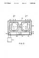
- FIGS. 2 and 3show the coating mechanism 107 in detail.
- Two processing units 10a and 10bare arranged in a common casing 40 and a resist nozzle 12 is located to be used commonly by the two processing units 10a and 10b.
- Both of the processing units 10a and 10bare arranged in the same atmosphere in the casing 40, thereby enabling the wafers W to be uniformly processed in both processing units 10a and 10b.
- Each of the processing units 10a and 10bis provided with a support 14 such as the spin chuck, which is fixed to the output shaft of a motor 20 so as to rotate that semiconductor wafer W at high speed which has been mounted and temporarily fixed on the spin chuck 14 by vacuum suction.
- a support 14such as the spin chuck
- the motor 20is a high performance one, excellent in acceleration, and it has a flange 22 at its top, by which it is fixed at an appropriate position in the coating mechanism or apparatus.
- the temperature of the flange 22can be adjusted by a temperature adjuster not to transmit the heat of the motor 20 above the flange 22.
- the semiconductor wafer W on the spin chuck 14is enclosed by a cup 16 to prevent the coating or resist liquid from being scattered outside the coating apparatus and onto the another adjacent semiconductor wafer W at the time when it is being coated with the resist liquid.
- the cup 16can move up and down and it is lifted to such a position as shown in FIG. 2 and stopped there at the time when the semiconductor wafer W is to be coated with the resist liquid, while it is lowered downward from the position at the time when the wafer W is to be carried into and out of the processing unit. Drain and exhaust pipes 18 and 19 are connected to the underside of each of the cups 16.
- the resist nozzle 12is intended to supply or drop the resist liquid onto the semiconductor wafer W at such a position that is above and substantially in the center of the semiconductor wafer W supported by the spin chuck 14 in each of the processing units 10a and 10b.
- the resist nozzle 12is freely moved or reciprocated between a waiting position A and the resist liquid dropping position B in each of the processing units 10a and 10b, while being supported by the tip of an arm 54 of a nozzle moving means 24.
- the cycle of coating the resist liquid onto the wafer W in one of the processing units 10a and 10bis shifted from that in the other processing unit by a half cycle.
- the resist nozzle 12is moved from its waiting position A to one of the positions B above the one processing unit 10a (or 10b) and caused to dispense the resist liquid onto the wafer W in this processing unit 10a (or 10b)
- itis first returned to its waiting position A and then moved to the other of the positions B above the other processing unit 10b (or 10a) to dispense the resist liquid onto the other wafer W in the other processing unit 10b (or 10a).
- a waiting trench 26which enables dummy dispensations of the resist liquid to be conducted through the resist nozzle 12 is arranged for this purpose at the waiting position A.
- the resist nozzle 12may thus be held in the resist liquid for a case where a waiting time is necessary during the exchange of wafers.
- the resist liquidis sucked back after the dispensation.
- the nozzle moving means 24is located between right and left rollers 44 and 46 and it includes an endless belt 48 which is driven right and left by a motor.
- a block 52movable right and left together with a part 48a of the belt 48 is attached to the belt 48.
- the arm 54is supported movable up and down by the moving block 52 and the resist nozzle 12 is supported at the tip of the arm 54.
- FIG. 8shows an example of detachably coupling the nozzle 24 with the arm 54.
- a projecting portion 82is integrally formed on the body of the nozzle 24 and a clamping hole 84 having a size corresponding to the portion 82 is formed on the tip of the arm 54.
- the portion 82is detachably held by a clamp member, which is controlled electrically, provided in the hole 84.
- the nozzle 12sits on the waiting trench 26 when freed by the arm 54.
- a volatile organic solvent 88is reserved in a pool 86 so as to decrease the hardening of the resist liquid.
- FIG. 4shows a line through which the resist liquid is supplied to the resist nozzle 12.
- This lineis a pipe 32 extending from a resist liquid vessel 28 and an N 2 pressurizing section 30 to the resist nozzle 12.
- the pipe 32includes a valve V1 and a suck-back valve V2 on the way thereof.
- the suck-back valve V2is intended to pull into the resist nozzle 12 that part of the resist liquid which is exposed from the tip of the resist nozzle 12 because of surface tension after the resist liquid is dispensed through the resist nozzle 12. The resist liquid at the tip of the resist nozzle 12 can be thus prevented from becoming hard.
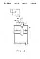
- a coating method according to the present inventionwill be described referring to a time chart shown in FIG. 5.
- the process described belowis automatically carried out by using a program stored in a computer.
- a wafer which is not processed yetis carried onto the spin chuck 14 in the one processing unit 10a.
- the waferis carried into the processing unit 10a in a direction F1 in FIG. 3 by the carrying means 110 (see FIG. 1). If the previous wafer which has been processed is still on the spin chuck 14 in the processing unit 10a, it is removed from the spin chuck 14 by one of the tweezers 112 and 113 of the carrying means 110 and the next wafer carried is mounted on the chuck 14 by the other tweezer (Step S1 in FIG. 5). The center of the wafer is automatically aligned with the center of rotation of the chuck 14 at this time.
- the arm 54is then moved to grip and pull the resist nozzle 12 out of the waiting trench 26 at the waiting position A and further moved above the wafer on the spin chuck 14 in the unit 10a while holding the resist nozzle 12.
- the resist liquidis dispensed or dropped onto the wafer through the resist nozzle 12 at this position, such as the center of the wafer.
- the resist nozzle 12is then moved to the waiting position A by the arm 54 and supported by the waiting trench 26 (Step S2).
- the chuck 14 in the unit 10ais rotated to uniformly scatter and coat the resist liquid on the wafer due to centrifugal force thus created (Step S3).
- the coating step caused by the rotation of the chuck 14is already advancing in the other unit 10b prior to the step S1 in such a manner that the processing cycle in the other unit 10b is half shifted from that in the one unit 10a (Step S4).
- Step S5After the coating is finished by the rotation of the spin chuck 14 in the other processing unit 10b, the cup 16 is lowered while the chuck 14 is lifted in this unit 10b (Step S5).
- a wafer which is not processed yetis carried onto the chuck 14 in the other unit 10b in a direction F2 in FIG. 3 by the carrying means 110.
- the wafer which has been processedis removed this time from the chuck 14 by the one 112 (or 113) of the tweezers 112 and 113 of the carrying means 110 and the next wafer which has been carried is mounted on the chuck 14 by the other 113 (or 112) (Step S6).
- the arm 54is then moved to grip and pick up the resist nozzle 12 out of the waiting trench 26 at the waiting position A and further moved above the wafer mounted on the chuck 14 in the unit 10b while holding the resist nozzle 12.
- the resist liquidis dropped onto the wafer through the resist nozzle 12 at this position.
- the resist nozzle 12is then again moved to the waiting position A by the arm 54 and supported by the waiting trench 26 (Step S7).
- the chuck 14 in the unit 10bis rotated to create centrifugal force, by which the resist liquid is uniformly scattered and coated on the wafer (Step S8).
- the coating caused by the rotation of the chuck 14is finished in the unit 10a after the coating caused by the rotation of the chuck 14 is started in the unit 10b, and the cup 16 is lowered while the chuck 14 is lifted in the unit 10a (Step S9).
- a wafer which is not processed yetis again carried onto the chuck 14 in the unit 10a by the carrying means 110 (Step S10).
- the interval at which the resist liquid is dispensed onto the wafer through the resist nozzle 12can be shortened and the hardening of the resist liquid at the tip of the resist nozzle 12 which has often been seen in the case where the interval of resist liquid dispensations is long can be thus reduced or prevented.
- this intervalis made shorter, as described above, there is created the possibility that the dummy dispensations at the waiting trench 26 become unnecessary.
- resist nozzle 12is enough for the coating apparatus and this enables the whole of the apparatus to be made simpler in structure.
- the resist nozzle 12is common to the two processing units and the resist liquid is thus made common to them. The uniformity of processes conducted in the two processing units can be thus expected.
- the present inventionis not limited to this mechanism but it can be applied to various kinds of coating apparatus such as those intended to coat the resist liquid, developer and magnetic matter to masks.
- the arm 54has been slid right and left in the above-described embodiment, it may be swung.
- the two processing unitshave been used in the above-described embodiment, three or more processing units may be used. Further, it may be arranged that the number of the nozzles 12 is made plural and that the number of the processing units governed by each of the nozzles 12 is selected. The operation of these coating apparatuses can be controlled by computers.
- FIGS. 6 and 7schematically show variations of the coating apparatus according to the present invention wherein three or more processing units are arranged relative to one nozzle.
- a resist nozzle 60is carried by a moving means 62 of the swing type.
- Three processing units 64a-64c and a waiting trench 66are arranged on that track on which the moving means 62 is swung.
- two resist nozzles 70a and 70bare carried by a moving means 72 which is provided with a pair of moving arms 71a and 71b extending in reverse directions from it and with a linear rail 73.
- Five processing units 74a-74e and a waiting trench 76are arranged on the side of the nozzle 70a and five processing units 75a-75e and a waiting trench 77 are arranged on the side of the nozzle 70b.
Landscapes
- Engineering & Computer Science (AREA)
- Physics & Mathematics (AREA)
- Condensed Matter Physics & Semiconductors (AREA)
- General Physics & Mathematics (AREA)
- Manufacturing & Machinery (AREA)
- Computer Hardware Design (AREA)
- Microelectronics & Electronic Packaging (AREA)
- Power Engineering (AREA)
- Coating Apparatus (AREA)
- Exposure Of Semiconductors, Excluding Electron Or Ion Beam Exposure (AREA)
- Application Of Or Painting With Fluid Materials (AREA)
Abstract
Description
Claims (8)
Priority Applications (1)
| Application Number | Priority Date | Filing Date | Title |
|---|---|---|---|
| US08/093,699US5416047A (en) | 1990-09-07 | 1993-07-20 | Method for applying process solution to substrates |
Applications Claiming Priority (2)
| Application Number | Priority Date | Filing Date | Title |
|---|---|---|---|
| JP2-237664 | 1990-09-07 | ||
| JP2237664AJP2843134B2 (en) | 1990-09-07 | 1990-09-07 | Coating device and coating method |
Related Child Applications (1)
| Application Number | Title | Priority Date | Filing Date |
|---|---|---|---|
| US08/093,699Continuation-In-PartUS5416047A (en) | 1990-09-07 | 1993-07-20 | Method for applying process solution to substrates |
Publications (1)
| Publication Number | Publication Date |
|---|---|
| US5250114Atrue US5250114A (en) | 1993-10-05 |
Family
ID=17018679
Family Applications (1)
| Application Number | Title | Priority Date | Filing Date |
|---|---|---|---|
| US07/755,781Expired - LifetimeUS5250114A (en) | 1990-09-07 | 1991-09-06 | Coating apparatus with nozzle moving means |
Country Status (3)
| Country | Link |
|---|---|
| US (1) | US5250114A (en) |
| JP (1) | JP2843134B2 (en) |
| KR (1) | KR0158211B1 (en) |
Cited By (28)
| Publication number | Priority date | Publication date | Assignee | Title |
|---|---|---|---|---|
| EP0688041A1 (en)* | 1994-06-17 | 1995-12-20 | Dainippon Screen Mfg. Co., Ltd. | Substrate processing apparatus |
| US5518542A (en)* | 1993-11-05 | 1996-05-21 | Tokyo Electron Limited | Double-sided substrate cleaning apparatus |
| US5578127A (en)* | 1993-02-08 | 1996-11-26 | Tokyo Electron Ltd | System for applying process liquid |
| US5756155A (en)* | 1996-01-22 | 1998-05-26 | Taiwan Semiconductor Manufacturing Company, Ltd. | Combination nozzle and vacuum hood that is self cleaning |
| US5902399A (en)* | 1995-07-27 | 1999-05-11 | Micron Technology, Inc. | Method and apparatus for improved coating of a semiconductor wafer |
| US5960225A (en)* | 1996-12-03 | 1999-09-28 | Tokyo Electron Limited | Substrate treatment apparatus |
| US6015513A (en)* | 1995-09-11 | 2000-01-18 | Charles Chang | Method of making lipstick samplers |
| US6033728A (en)* | 1993-05-13 | 2000-03-07 | Fujitsu Limited | Apparatus for spin coating, a method for spin coating and a method for manufacturing semiconductor device |
| US6416579B1 (en)* | 1999-01-13 | 2002-07-09 | Erich Thallner | Apparatus for treating silicon wafers |
| US6444029B1 (en)* | 1998-06-24 | 2002-09-03 | Tokyo Electron Limited | Multistage spin type substrate processing system |
| US6551403B1 (en)* | 2000-05-25 | 2003-04-22 | Nec Electronics, Inc. | Solvent pre-wet system for wafers |
| US20030202871A1 (en)* | 1994-04-28 | 2003-10-30 | Thompson Raymon F. | Semiconductor processing system with wafer container docking and loading station |
| US20040020601A1 (en)* | 2000-02-10 | 2004-02-05 | Applied Materials, Inc. | Process and an integrated tool for low k dielectric deposition including a pecvd capping module |
| US6796517B1 (en) | 2000-03-09 | 2004-09-28 | Advanced Micro Devices, Inc. | Apparatus for the application of developing solution to a semiconductor wafer |
| US20060130747A1 (en)* | 2004-12-22 | 2006-06-22 | Applied Materials, Inc. | Coat/develop module with shared dispense |
| WO2006069348A3 (en)* | 2004-12-22 | 2006-09-28 | Applied Materials Inc | Coat/develop module with shared dispense |
| KR100681315B1 (en)* | 2004-12-28 | 2007-02-15 | 동부일렉트로닉스 주식회사 | Semiconductor wafer developing apparatus |
| US20070197050A1 (en)* | 2006-02-22 | 2007-08-23 | Shirley Paul D | Systems and methods for manipulating liquid films on semiconductor substrates |
| US20070238028A1 (en)* | 2004-04-20 | 2007-10-11 | Tokyo Electron Limited | Substrate Treatment Method and Substrate Treatment Apparatus |
| US7651306B2 (en) | 2004-12-22 | 2010-01-26 | Applied Materials, Inc. | Cartesian robot cluster tool architecture |
| US7699021B2 (en) | 2004-12-22 | 2010-04-20 | Sokudo Co., Ltd. | Cluster tool substrate throughput optimization |
| US7798764B2 (en) | 2005-12-22 | 2010-09-21 | Applied Materials, Inc. | Substrate processing sequence in a cartesian robot cluster tool |
| US7819079B2 (en) | 2004-12-22 | 2010-10-26 | Applied Materials, Inc. | Cartesian cluster tool configuration for lithography type processes |
| US20100293806A1 (en)* | 2006-01-18 | 2010-11-25 | Liu Zhi Lewis | Systems and methods for drying a rotating substrate |
| US8636915B2 (en) | 2010-07-23 | 2014-01-28 | Tokyo Electron Limited | Liquid processing apparatus and liquid processing method |
| US20160026086A1 (en)* | 2014-07-23 | 2016-01-28 | Tokyo Electron Limited | Developing apparatus |
| US9555437B2 (en) | 2012-08-31 | 2017-01-31 | SCREEN Holdings Co., Ltd. | Substrate processing apparatus |
| CN108828898A (en)* | 2017-08-02 | 2018-11-16 | 长鑫存储技术有限公司 | Method for improving edge defects in photoresist coating process |
Families Citing this family (6)
| Publication number | Priority date | Publication date | Assignee | Title |
|---|---|---|---|---|
| TW294821B (en)* | 1994-09-09 | 1997-01-01 | Tokyo Electron Co Ltd | |
| US6068881A (en)* | 1998-05-29 | 2000-05-30 | International Business Machines Corporation | Spin-apply tool having exhaust ring |
| JP5442969B2 (en)* | 2008-07-28 | 2014-03-19 | 株式会社Sokudo | Substrate processing unit, substrate processing apparatus, and nozzle position control method |
| JP5442968B2 (en)* | 2008-07-28 | 2014-03-19 | 株式会社Sokudo | Substrate processing unit and substrate processing apparatus |
| JP5545693B2 (en)* | 2008-10-01 | 2014-07-09 | 株式会社Sokudo | Development processing equipment |
| JP5672204B2 (en)* | 2011-09-13 | 2015-02-18 | 東京エレクトロン株式会社 | Liquid processing apparatus, liquid processing method, and storage medium |
Citations (13)
| Publication number | Priority date | Publication date | Assignee | Title |
|---|---|---|---|---|
| US3904339A (en)* | 1972-02-03 | 1975-09-09 | Owens Corning Fiberglass Corp | Apparatus for depositing materials on surfaces of revolution |
| US4158343A (en)* | 1977-09-27 | 1979-06-19 | Nordson Corporation | Coater |
| US4190015A (en)* | 1977-12-08 | 1980-02-26 | Machine Technology, Inc. | Apparatus for dispensing liquid to spinning workpieces |
| JPS58124241A (en)* | 1982-01-21 | 1983-07-23 | Nec Corp | Developing device for semiconductor substrate |
| US4416213A (en)* | 1981-02-14 | 1983-11-22 | Tazmo Co., Ltd. | Rotary coating apparatus |
| JPS62195118A (en)* | 1986-02-21 | 1987-08-27 | Hitachi Ltd | Photoresist developing device |
| JPH01276722A (en)* | 1988-04-28 | 1989-11-07 | Nec Corp | Substrate treatment device |
| US4889069A (en)* | 1987-11-23 | 1989-12-26 | Tazmo Co., Ltd. | Substrate coating equipment |
| US4941426A (en)* | 1987-09-18 | 1990-07-17 | Tokyo Ohka Kogyo Co., Ltd. | Thin-film coating apparatus |
| US4989345A (en)* | 1989-12-18 | 1991-02-05 | Gill Jr Gerald L | Centrifugal spin dryer for semiconductor wafer |
| US5002008A (en)* | 1988-05-27 | 1991-03-26 | Tokyo Electron Limited | Coating apparatus and method for applying a liquid to a semiconductor wafer, including selecting a nozzle in a stand-by state |
| US5061144A (en)* | 1988-11-30 | 1991-10-29 | Tokyo Electron Limited | Resist process apparatus |
| US5095848A (en)* | 1989-05-02 | 1992-03-17 | Mitsubishi Denki Kabushiki Kaisha | Spin coating apparatus using a tilting chuck |
- 1990
- 1990-09-07JPJP2237664Apatent/JP2843134B2/ennot_activeExpired - Lifetime
- 1991
- 1991-09-06USUS07/755,781patent/US5250114A/ennot_activeExpired - Lifetime
- 1991-09-06KRKR1019910015595Apatent/KR0158211B1/ennot_activeExpired - Lifetime
Patent Citations (14)
| Publication number | Priority date | Publication date | Assignee | Title |
|---|---|---|---|---|
| US3904339A (en)* | 1972-02-03 | 1975-09-09 | Owens Corning Fiberglass Corp | Apparatus for depositing materials on surfaces of revolution |
| US4158343A (en)* | 1977-09-27 | 1979-06-19 | Nordson Corporation | Coater |
| US4190015A (en)* | 1977-12-08 | 1980-02-26 | Machine Technology, Inc. | Apparatus for dispensing liquid to spinning workpieces |
| US4416213A (en)* | 1981-02-14 | 1983-11-22 | Tazmo Co., Ltd. | Rotary coating apparatus |
| JPS58124241A (en)* | 1982-01-21 | 1983-07-23 | Nec Corp | Developing device for semiconductor substrate |
| JPS62195118A (en)* | 1986-02-21 | 1987-08-27 | Hitachi Ltd | Photoresist developing device |
| US4941426A (en)* | 1987-09-18 | 1990-07-17 | Tokyo Ohka Kogyo Co., Ltd. | Thin-film coating apparatus |
| US4889069A (en)* | 1987-11-23 | 1989-12-26 | Tazmo Co., Ltd. | Substrate coating equipment |
| JPH01276722A (en)* | 1988-04-28 | 1989-11-07 | Nec Corp | Substrate treatment device |
| US5002008A (en)* | 1988-05-27 | 1991-03-26 | Tokyo Electron Limited | Coating apparatus and method for applying a liquid to a semiconductor wafer, including selecting a nozzle in a stand-by state |
| US5089305A (en)* | 1988-05-27 | 1992-02-18 | Tokyo Electron Limited | Coating apparatus and method for applying a liquid to a semiconductor wafer including selecting a nozzle on a stand by state |
| US5061144A (en)* | 1988-11-30 | 1991-10-29 | Tokyo Electron Limited | Resist process apparatus |
| US5095848A (en)* | 1989-05-02 | 1992-03-17 | Mitsubishi Denki Kabushiki Kaisha | Spin coating apparatus using a tilting chuck |
| US4989345A (en)* | 1989-12-18 | 1991-02-05 | Gill Jr Gerald L | Centrifugal spin dryer for semiconductor wafer |
Cited By (61)
| Publication number | Priority date | Publication date | Assignee | Title |
|---|---|---|---|---|
| US5578127A (en)* | 1993-02-08 | 1996-11-26 | Tokyo Electron Ltd | System for applying process liquid |
| US6033728A (en)* | 1993-05-13 | 2000-03-07 | Fujitsu Limited | Apparatus for spin coating, a method for spin coating and a method for manufacturing semiconductor device |
| US5518542A (en)* | 1993-11-05 | 1996-05-21 | Tokyo Electron Limited | Double-sided substrate cleaning apparatus |
| US20030202871A1 (en)* | 1994-04-28 | 2003-10-30 | Thompson Raymon F. | Semiconductor processing system with wafer container docking and loading station |
| US6960257B2 (en)* | 1994-04-28 | 2005-11-01 | Semitool, Inc. | Semiconductor processing system with wafer container docking and loading station |
| EP0688041A1 (en)* | 1994-06-17 | 1995-12-20 | Dainippon Screen Mfg. Co., Ltd. | Substrate processing apparatus |
| US5639301A (en)* | 1994-06-17 | 1997-06-17 | Dainippon Screen Mfg. Co., Ltd. | Processing apparatus having parts for thermal and non-thermal treatment of substrates |
| US6666917B2 (en)* | 1995-07-27 | 2003-12-23 | Micron Technology, Inc. | Apparatus for coating of a semiconductor wafer |
| US5902399A (en)* | 1995-07-27 | 1999-05-11 | Micron Technology, Inc. | Method and apparatus for improved coating of a semiconductor wafer |
| US20060257561A1 (en)* | 1995-07-27 | 2006-11-16 | Micron Technology, Inc. | Method and apparatus for coating a wafer |
| US6423380B1 (en)* | 1995-07-27 | 2002-07-23 | Micron Technology, Inc. | Method of coating a semiconductor wafer |
| US20040052956A1 (en)* | 1995-07-27 | 2004-03-18 | Courtenay Robert William | Method and apparatus for coating a wafer |
| US6015513A (en)* | 1995-09-11 | 2000-01-18 | Charles Chang | Method of making lipstick samplers |
| US5756155A (en)* | 1996-01-22 | 1998-05-26 | Taiwan Semiconductor Manufacturing Company, Ltd. | Combination nozzle and vacuum hood that is self cleaning |
| US5960225A (en)* | 1996-12-03 | 1999-09-28 | Tokyo Electron Limited | Substrate treatment apparatus |
| US6444029B1 (en)* | 1998-06-24 | 2002-09-03 | Tokyo Electron Limited | Multistage spin type substrate processing system |
| US6416579B1 (en)* | 1999-01-13 | 2002-07-09 | Erich Thallner | Apparatus for treating silicon wafers |
| US20040020601A1 (en)* | 2000-02-10 | 2004-02-05 | Applied Materials, Inc. | Process and an integrated tool for low k dielectric deposition including a pecvd capping module |
| US6796517B1 (en) | 2000-03-09 | 2004-09-28 | Advanced Micro Devices, Inc. | Apparatus for the application of developing solution to a semiconductor wafer |
| US6551403B1 (en)* | 2000-05-25 | 2003-04-22 | Nec Electronics, Inc. | Solvent pre-wet system for wafers |
| US7819076B2 (en)* | 2004-04-20 | 2010-10-26 | Tokyo Electron Limited | Substrate treatment method and substrate treatment apparatus |
| US20100316961A1 (en)* | 2004-04-20 | 2010-12-16 | Tokyo Electon Limited | Substrate treatment method and substrate treatment apparatus |
| US7989156B2 (en) | 2004-04-20 | 2011-08-02 | Tokyo Electron Limited | Substrate treatment method and substrate treatment apparatus |
| US20070238028A1 (en)* | 2004-04-20 | 2007-10-11 | Tokyo Electron Limited | Substrate Treatment Method and Substrate Treatment Apparatus |
| US20060134340A1 (en)* | 2004-12-22 | 2006-06-22 | Applied Materials, Inc. A Delaware Corporation | Coat/develop module with independent stations |
| US7651306B2 (en) | 2004-12-22 | 2010-01-26 | Applied Materials, Inc. | Cartesian robot cluster tool architecture |
| US7255747B2 (en) | 2004-12-22 | 2007-08-14 | Sokudo Co., Ltd. | Coat/develop module with independent stations |
| US7357842B2 (en) | 2004-12-22 | 2008-04-15 | Sokudo Co., Ltd. | Cluster tool architecture for processing a substrate |
| US7396412B2 (en) | 2004-12-22 | 2008-07-08 | Sokudo Co., Ltd. | Coat/develop module with shared dispense |
| US20080296316A1 (en)* | 2004-12-22 | 2008-12-04 | Sokudo Co., Ltd. | Coat/develop module with shared dispense |
| US8550031B2 (en) | 2004-12-22 | 2013-10-08 | Applied Materials, Inc. | Cluster tool architecture for processing a substrate |
| US7819079B2 (en) | 2004-12-22 | 2010-10-26 | Applied Materials, Inc. | Cartesian cluster tool configuration for lithography type processes |
| KR100925898B1 (en)* | 2004-12-22 | 2009-11-09 | 가부시키가이샤 소쿠도 | Coat/develop module with shared dispense |
| US8911193B2 (en) | 2004-12-22 | 2014-12-16 | Applied Materials, Inc. | Substrate processing sequence in a cartesian robot cluster tool |
| US7694647B2 (en) | 2004-12-22 | 2010-04-13 | Applied Materials, Inc. | Cluster tool architecture for processing a substrate |
| US7699021B2 (en) | 2004-12-22 | 2010-04-20 | Sokudo Co., Ltd. | Cluster tool substrate throughput optimization |
| WO2006069348A3 (en)* | 2004-12-22 | 2006-09-28 | Applied Materials Inc | Coat/develop module with shared dispense |
| US7743728B2 (en) | 2004-12-22 | 2010-06-29 | Applied Materials, Inc. | Cluster tool architecture for processing a substrate |
| US7925377B2 (en) | 2004-12-22 | 2011-04-12 | Applied Materials, Inc. | Cluster tool architecture for processing a substrate |
| US20060130747A1 (en)* | 2004-12-22 | 2006-06-22 | Applied Materials, Inc. | Coat/develop module with shared dispense |
| KR100681315B1 (en)* | 2004-12-28 | 2007-02-15 | 동부일렉트로닉스 주식회사 | Semiconductor wafer developing apparatus |
| US8066466B2 (en) | 2005-12-22 | 2011-11-29 | Applied Materials, Inc. | Substrate processing sequence in a Cartesian robot cluster tool |
| US7798764B2 (en) | 2005-12-22 | 2010-09-21 | Applied Materials, Inc. | Substrate processing sequence in a cartesian robot cluster tool |
| US8739429B2 (en) | 2006-01-18 | 2014-06-03 | Akrion Systems, Llc | Systems and methods for drying a rotating substrate |
| US9337065B2 (en) | 2006-01-18 | 2016-05-10 | Akrion Systems, Llc | Systems and methods for drying a rotating substrate |
| US8056253B2 (en)* | 2006-01-18 | 2011-11-15 | Akrion Systems Llc | Systems and methods for drying a rotating substrate |
| US20100293806A1 (en)* | 2006-01-18 | 2010-11-25 | Liu Zhi Lewis | Systems and methods for drying a rotating substrate |
| US8276291B2 (en) | 2006-01-18 | 2012-10-02 | Akrion Systems Llc | Systems and methods for drying a rotating substrate |
| US20090068848A1 (en)* | 2006-02-22 | 2009-03-12 | Micron Technology, Inc. | Systems and methods for manipulating liquid films on semiconductor substrates |
| US7470638B2 (en) | 2006-02-22 | 2008-12-30 | Micron Technology, Inc. | Systems and methods for manipulating liquid films on semiconductor substrates |
| US20070197050A1 (en)* | 2006-02-22 | 2007-08-23 | Shirley Paul D | Systems and methods for manipulating liquid films on semiconductor substrates |
| US7737055B2 (en) | 2006-02-22 | 2010-06-15 | Micron Technology, Inc. | Systems and methods for manipulating liquid films on semiconductor substrates |
| US8636915B2 (en) | 2010-07-23 | 2014-01-28 | Tokyo Electron Limited | Liquid processing apparatus and liquid processing method |
| US9555437B2 (en) | 2012-08-31 | 2017-01-31 | SCREEN Holdings Co., Ltd. | Substrate processing apparatus |
| US10026627B2 (en) | 2012-08-31 | 2018-07-17 | SCREEN Holdings Co., Ltd. | Substrate processing apparatus |
| US10707096B2 (en) | 2012-08-31 | 2020-07-07 | SCREEN Holdings Co., Ltd. | Substrate processing apparatus |
| US10707097B2 (en) | 2012-08-31 | 2020-07-07 | SCREEN Holdings Co., Ltd. | Substrate processing apparatus |
| US10734252B2 (en) | 2012-08-31 | 2020-08-04 | SCREEN Holdings Co., Ltd. | Substrate processing apparatus |
| US20160026086A1 (en)* | 2014-07-23 | 2016-01-28 | Tokyo Electron Limited | Developing apparatus |
| US9625821B2 (en)* | 2014-07-23 | 2017-04-18 | Tokyo Electron Limited | Developing apparatus |
| CN108828898A (en)* | 2017-08-02 | 2018-11-16 | 长鑫存储技术有限公司 | Method for improving edge defects in photoresist coating process |
Also Published As
| Publication number | Publication date |
|---|---|
| KR0158211B1 (en) | 1999-02-18 |
| KR920007088A (en) | 1992-04-28 |
| JPH04118074A (en) | 1992-04-20 |
| JP2843134B2 (en) | 1999-01-06 |
Similar Documents
| Publication | Publication Date | Title |
|---|---|---|
| US5250114A (en) | Coating apparatus with nozzle moving means | |
| US6471421B2 (en) | Developing unit and developing method | |
| KR100873720B1 (en) | Developing Method and Developing Device | |
| US5416047A (en) | Method for applying process solution to substrates | |
| KR101609885B1 (en) | Liquid processing apparatus | |
| US6364547B1 (en) | Solution processing apparatus | |
| JPH11260717A (en) | Resist coating method and apparatus | |
| US20030205196A1 (en) | Substrate processing apparatus and substrate processing method | |
| JP2003045788A (en) | Wafer processing method and apparatus | |
| JP2001284206A (en) | Device and method for treating substrate | |
| JP2001307984A (en) | Resist application method and resist application device | |
| KR100637952B1 (en) | Coating film forming method and coating device | |
| JP2000195773A (en) | Development processing method and developer | |
| JP3766177B2 (en) | Substrate processing apparatus and substrate cleaning apparatus | |
| JP3164739B2 (en) | Method and apparatus for forming coating film | |
| JPH08168715A (en) | Rotary coating device and method thereof | |
| JP3266816B2 (en) | Coating device | |
| JP2926593B2 (en) | Substrate processing apparatus, resist processing apparatus, substrate processing method, and resist processing method | |
| JPH10247621A (en) | Resist treatment method and its system | |
| JP3527459B2 (en) | Coating film forming method and coating processing apparatus | |
| JP2001168167A (en) | Treating system and method | |
| JP2001044100A (en) | Development treating method of substrate | |
| JP2901746B2 (en) | Heat treatment apparatus and heat treatment method | |
| JP4050180B2 (en) | Substrate processing method | |
| JP3962490B2 (en) | Development processing apparatus and development processing method |
Legal Events
| Date | Code | Title | Description |
|---|---|---|---|
| AS | Assignment | Owner name:TOKYO ELECTRON LIMITED, JAPAN Free format text:ASSIGNMENT OF ASSIGNORS INTEREST.;ASSIGNORS:KONISHI, NOBUO;TAKAMORI, HIDEYUKI;AKIMOTO, MASAMI;AND OTHERS;REEL/FRAME:006404/0348;SIGNING DATES FROM 19910820 TO 19910823 Owner name:TOKYO ELECTRON KYUSHU LIMITED, JAPAN Free format text:ASSIGNMENT OF ASSIGNORS INTEREST.;ASSIGNORS:KONISHI, NOBUO;TAKAMORI, HIDEYUKI;AKIMOTO, MASAMI;AND OTHERS;REEL/FRAME:006404/0348;SIGNING DATES FROM 19910820 TO 19910823 | |
| STCF | Information on status: patent grant | Free format text:PATENTED CASE | |
| FEPP | Fee payment procedure | Free format text:PAYOR NUMBER ASSIGNED (ORIGINAL EVENT CODE: ASPN); ENTITY STATUS OF PATENT OWNER: LARGE ENTITY | |
| FPAY | Fee payment | Year of fee payment:4 | |
| AS | Assignment | Owner name:TOKYO ELECTRON LIMITED, JAPAN Free format text:ASSIGNMENT OF ASSIGNORS INTEREST;ASSIGNOR:TOKYO ELECTRON KYUSHU LIMITED;REEL/FRAME:009453/0220 Effective date:19980513 | |
| FEPP | Fee payment procedure | Free format text:PAYER NUMBER DE-ASSIGNED (ORIGINAL EVENT CODE: RMPN); ENTITY STATUS OF PATENT OWNER: LARGE ENTITY Free format text:PAYOR NUMBER ASSIGNED (ORIGINAL EVENT CODE: ASPN); ENTITY STATUS OF PATENT OWNER: LARGE ENTITY | |
| FPAY | Fee payment | Year of fee payment:8 | |
| FPAY | Fee payment | Year of fee payment:12 |