US5247423A - Stacking three dimensional leadless multi-chip module and method for making the same - Google Patents
Stacking three dimensional leadless multi-chip module and method for making the sameDownload PDFInfo
- Publication number
- US5247423A US5247423AUS07/887,963US88796392AUS5247423AUS 5247423 AUS5247423 AUS 5247423AUS 88796392 AUS88796392 AUS 88796392AUS 5247423 AUS5247423 AUS 5247423A
- Authority
- US
- United States
- Prior art keywords
- semiconductor
- flexible substrate
- pair
- semiconductor die
- package body
- Prior art date
- Legal status (The legal status is an assumption and is not a legal conclusion. Google has not performed a legal analysis and makes no representation as to the accuracy of the status listed.)
- Expired - Lifetime
Links
Images


Classifications
- H—ELECTRICITY
- H01—ELECTRIC ELEMENTS
- H01L—SEMICONDUCTOR DEVICES NOT COVERED BY CLASS H10
- H01L23/00—Details of semiconductor or other solid state devices
- H01L23/48—Arrangements for conducting electric current to or from the solid state body in operation, e.g. leads, terminal arrangements ; Selection of materials therefor
- H01L23/488—Arrangements for conducting electric current to or from the solid state body in operation, e.g. leads, terminal arrangements ; Selection of materials therefor consisting of soldered or bonded constructions
- H01L23/498—Leads, i.e. metallisations or lead-frames on insulating substrates, e.g. chip carriers
- H01L23/4985—Flexible insulating substrates
- H—ELECTRICITY
- H01—ELECTRIC ELEMENTS
- H01L—SEMICONDUCTOR DEVICES NOT COVERED BY CLASS H10
- H01L25/00—Assemblies consisting of a plurality of semiconductor or other solid state devices
- H—ELECTRICITY
- H01—ELECTRIC ELEMENTS
- H01L—SEMICONDUCTOR DEVICES NOT COVERED BY CLASS H10
- H01L23/00—Details of semiconductor or other solid state devices
- H01L23/28—Encapsulations, e.g. encapsulating layers, coatings, e.g. for protection
- H01L23/31—Encapsulations, e.g. encapsulating layers, coatings, e.g. for protection characterised by the arrangement or shape
- H01L23/3107—Encapsulations, e.g. encapsulating layers, coatings, e.g. for protection characterised by the arrangement or shape the device being completely enclosed
- H01L23/3121—Encapsulations, e.g. encapsulating layers, coatings, e.g. for protection characterised by the arrangement or shape the device being completely enclosed a substrate forming part of the encapsulation
- H—ELECTRICITY
- H01—ELECTRIC ELEMENTS
- H01L—SEMICONDUCTOR DEVICES NOT COVERED BY CLASS H10
- H01L25/00—Assemblies consisting of a plurality of semiconductor or other solid state devices
- H01L25/03—Assemblies consisting of a plurality of semiconductor or other solid state devices all the devices being of a type provided for in a single subclass of subclasses H10B, H10D, H10F, H10H, H10K or H10N, e.g. assemblies of rectifier diodes
- H01L25/04—Assemblies consisting of a plurality of semiconductor or other solid state devices all the devices being of a type provided for in a single subclass of subclasses H10B, H10D, H10F, H10H, H10K or H10N, e.g. assemblies of rectifier diodes the devices not having separate containers
- H01L25/065—Assemblies consisting of a plurality of semiconductor or other solid state devices all the devices being of a type provided for in a single subclass of subclasses H10B, H10D, H10F, H10H, H10K or H10N, e.g. assemblies of rectifier diodes the devices not having separate containers the devices being of a type provided for in group H10D89/00
- H01L25/0657—Stacked arrangements of devices
- H—ELECTRICITY
- H01—ELECTRIC ELEMENTS
- H01L—SEMICONDUCTOR DEVICES NOT COVERED BY CLASS H10
- H01L25/00—Assemblies consisting of a plurality of semiconductor or other solid state devices
- H01L25/03—Assemblies consisting of a plurality of semiconductor or other solid state devices all the devices being of a type provided for in a single subclass of subclasses H10B, H10D, H10F, H10H, H10K or H10N, e.g. assemblies of rectifier diodes
- H01L25/10—Assemblies consisting of a plurality of semiconductor or other solid state devices all the devices being of a type provided for in a single subclass of subclasses H10B, H10D, H10F, H10H, H10K or H10N, e.g. assemblies of rectifier diodes the devices having separate containers
- H01L25/105—Assemblies consisting of a plurality of semiconductor or other solid state devices all the devices being of a type provided for in a single subclass of subclasses H10B, H10D, H10F, H10H, H10K or H10N, e.g. assemblies of rectifier diodes the devices having separate containers the devices being integrated devices of class H10
- H—ELECTRICITY
- H05—ELECTRIC TECHNIQUES NOT OTHERWISE PROVIDED FOR
- H05K—PRINTED CIRCUITS; CASINGS OR CONSTRUCTIONAL DETAILS OF ELECTRIC APPARATUS; MANUFACTURE OF ASSEMBLAGES OF ELECTRICAL COMPONENTS
- H05K1/00—Printed circuits
- H05K1/02—Details
- H05K1/14—Structural association of two or more printed circuits
- H05K1/144—Stacked arrangements of planar printed circuit boards
- H—ELECTRICITY
- H05—ELECTRIC TECHNIQUES NOT OTHERWISE PROVIDED FOR
- H05K—PRINTED CIRCUITS; CASINGS OR CONSTRUCTIONAL DETAILS OF ELECTRIC APPARATUS; MANUFACTURE OF ASSEMBLAGES OF ELECTRICAL COMPONENTS
- H05K7/00—Constructional details common to different types of electric apparatus
- H05K7/20—Modifications to facilitate cooling, ventilating, or heating
- H—ELECTRICITY
- H01—ELECTRIC ELEMENTS
- H01L—SEMICONDUCTOR DEVICES NOT COVERED BY CLASS H10
- H01L2224/00—Indexing scheme for arrangements for connecting or disconnecting semiconductor or solid-state bodies and methods related thereto as covered by H01L24/00
- H01L2224/01—Means for bonding being attached to, or being formed on, the surface to be connected, e.g. chip-to-package, die-attach, "first-level" interconnects; Manufacturing methods related thereto
- H01L2224/26—Layer connectors, e.g. plate connectors, solder or adhesive layers; Manufacturing methods related thereto
- H01L2224/31—Structure, shape, material or disposition of the layer connectors after the connecting process
- H01L2224/32—Structure, shape, material or disposition of the layer connectors after the connecting process of an individual layer connector
- H01L2224/321—Disposition
- H01L2224/32151—Disposition the layer connector connecting between a semiconductor or solid-state body and an item not being a semiconductor or solid-state body, e.g. chip-to-substrate, chip-to-passive
- H01L2224/32221—Disposition the layer connector connecting between a semiconductor or solid-state body and an item not being a semiconductor or solid-state body, e.g. chip-to-substrate, chip-to-passive the body and the item being stacked
- H01L2224/32225—Disposition the layer connector connecting between a semiconductor or solid-state body and an item not being a semiconductor or solid-state body, e.g. chip-to-substrate, chip-to-passive the body and the item being stacked the item being non-metallic, e.g. insulating substrate with or without metallisation
- H—ELECTRICITY
- H01—ELECTRIC ELEMENTS
- H01L—SEMICONDUCTOR DEVICES NOT COVERED BY CLASS H10
- H01L2224/00—Indexing scheme for arrangements for connecting or disconnecting semiconductor or solid-state bodies and methods related thereto as covered by H01L24/00
- H01L2224/01—Means for bonding being attached to, or being formed on, the surface to be connected, e.g. chip-to-package, die-attach, "first-level" interconnects; Manufacturing methods related thereto
- H01L2224/42—Wire connectors; Manufacturing methods related thereto
- H01L2224/47—Structure, shape, material or disposition of the wire connectors after the connecting process
- H01L2224/48—Structure, shape, material or disposition of the wire connectors after the connecting process of an individual wire connector
- H01L2224/4805—Shape
- H01L2224/4809—Loop shape
- H01L2224/48091—Arched
- H—ELECTRICITY
- H01—ELECTRIC ELEMENTS
- H01L—SEMICONDUCTOR DEVICES NOT COVERED BY CLASS H10
- H01L2224/00—Indexing scheme for arrangements for connecting or disconnecting semiconductor or solid-state bodies and methods related thereto as covered by H01L24/00
- H01L2224/01—Means for bonding being attached to, or being formed on, the surface to be connected, e.g. chip-to-package, die-attach, "first-level" interconnects; Manufacturing methods related thereto
- H01L2224/42—Wire connectors; Manufacturing methods related thereto
- H01L2224/47—Structure, shape, material or disposition of the wire connectors after the connecting process
- H01L2224/48—Structure, shape, material or disposition of the wire connectors after the connecting process of an individual wire connector
- H01L2224/481—Disposition
- H01L2224/48151—Connecting between a semiconductor or solid-state body and an item not being a semiconductor or solid-state body, e.g. chip-to-substrate, chip-to-passive
- H01L2224/48221—Connecting between a semiconductor or solid-state body and an item not being a semiconductor or solid-state body, e.g. chip-to-substrate, chip-to-passive the body and the item being stacked
- H01L2224/48225—Connecting between a semiconductor or solid-state body and an item not being a semiconductor or solid-state body, e.g. chip-to-substrate, chip-to-passive the body and the item being stacked the item being non-metallic, e.g. insulating substrate with or without metallisation
- H01L2224/48227—Connecting between a semiconductor or solid-state body and an item not being a semiconductor or solid-state body, e.g. chip-to-substrate, chip-to-passive the body and the item being stacked the item being non-metallic, e.g. insulating substrate with or without metallisation connecting the wire to a bond pad of the item
- H—ELECTRICITY
- H01—ELECTRIC ELEMENTS
- H01L—SEMICONDUCTOR DEVICES NOT COVERED BY CLASS H10
- H01L2225/00—Details relating to assemblies covered by the group H01L25/00 but not provided for in its subgroups
- H01L2225/03—All the devices being of a type provided for in the same main group of the same subclass of class H10, e.g. assemblies of rectifier diodes
- H01L2225/04—All the devices being of a type provided for in the same main group of the same subclass of class H10, e.g. assemblies of rectifier diodes the devices not having separate containers
- H01L2225/065—All the devices being of a type provided for in the same main group of the same subclass of class H10
- H01L2225/06503—Stacked arrangements of devices
- H01L2225/0651—Wire or wire-like electrical connections from device to substrate
- H—ELECTRICITY
- H01—ELECTRIC ELEMENTS
- H01L—SEMICONDUCTOR DEVICES NOT COVERED BY CLASS H10
- H01L2225/00—Details relating to assemblies covered by the group H01L25/00 but not provided for in its subgroups
- H01L2225/03—All the devices being of a type provided for in the same main group of the same subclass of class H10, e.g. assemblies of rectifier diodes
- H01L2225/04—All the devices being of a type provided for in the same main group of the same subclass of class H10, e.g. assemblies of rectifier diodes the devices not having separate containers
- H01L2225/065—All the devices being of a type provided for in the same main group of the same subclass of class H10
- H01L2225/06503—Stacked arrangements of devices
- H01L2225/0652—Bump or bump-like direct electrical connections from substrate to substrate
- H—ELECTRICITY
- H01—ELECTRIC ELEMENTS
- H01L—SEMICONDUCTOR DEVICES NOT COVERED BY CLASS H10
- H01L2225/00—Details relating to assemblies covered by the group H01L25/00 but not provided for in its subgroups
- H01L2225/03—All the devices being of a type provided for in the same main group of the same subclass of class H10, e.g. assemblies of rectifier diodes
- H01L2225/04—All the devices being of a type provided for in the same main group of the same subclass of class H10, e.g. assemblies of rectifier diodes the devices not having separate containers
- H01L2225/065—All the devices being of a type provided for in the same main group of the same subclass of class H10
- H01L2225/06503—Stacked arrangements of devices
- H01L2225/06527—Special adaptation of electrical connections, e.g. rewiring, engineering changes, pressure contacts, layout
- H—ELECTRICITY
- H01—ELECTRIC ELEMENTS
- H01L—SEMICONDUCTOR DEVICES NOT COVERED BY CLASS H10
- H01L2225/00—Details relating to assemblies covered by the group H01L25/00 but not provided for in its subgroups
- H01L2225/03—All the devices being of a type provided for in the same main group of the same subclass of class H10, e.g. assemblies of rectifier diodes
- H01L2225/04—All the devices being of a type provided for in the same main group of the same subclass of class H10, e.g. assemblies of rectifier diodes the devices not having separate containers
- H01L2225/065—All the devices being of a type provided for in the same main group of the same subclass of class H10
- H01L2225/06503—Stacked arrangements of devices
- H01L2225/06551—Conductive connections on the side of the device
- H—ELECTRICITY
- H01—ELECTRIC ELEMENTS
- H01L—SEMICONDUCTOR DEVICES NOT COVERED BY CLASS H10
- H01L2225/00—Details relating to assemblies covered by the group H01L25/00 but not provided for in its subgroups
- H01L2225/03—All the devices being of a type provided for in the same main group of the same subclass of class H10, e.g. assemblies of rectifier diodes
- H01L2225/04—All the devices being of a type provided for in the same main group of the same subclass of class H10, e.g. assemblies of rectifier diodes the devices not having separate containers
- H01L2225/065—All the devices being of a type provided for in the same main group of the same subclass of class H10
- H01L2225/06503—Stacked arrangements of devices
- H01L2225/06555—Geometry of the stack, e.g. form of the devices, geometry to facilitate stacking
- H—ELECTRICITY
- H01—ELECTRIC ELEMENTS
- H01L—SEMICONDUCTOR DEVICES NOT COVERED BY CLASS H10
- H01L2225/00—Details relating to assemblies covered by the group H01L25/00 but not provided for in its subgroups
- H01L2225/03—All the devices being of a type provided for in the same main group of the same subclass of class H10, e.g. assemblies of rectifier diodes
- H01L2225/04—All the devices being of a type provided for in the same main group of the same subclass of class H10, e.g. assemblies of rectifier diodes the devices not having separate containers
- H01L2225/065—All the devices being of a type provided for in the same main group of the same subclass of class H10
- H01L2225/06503—Stacked arrangements of devices
- H01L2225/06572—Auxiliary carrier between devices, the carrier having an electrical connection structure
- H—ELECTRICITY
- H01—ELECTRIC ELEMENTS
- H01L—SEMICONDUCTOR DEVICES NOT COVERED BY CLASS H10
- H01L2225/00—Details relating to assemblies covered by the group H01L25/00 but not provided for in its subgroups
- H01L2225/03—All the devices being of a type provided for in the same main group of the same subclass of class H10, e.g. assemblies of rectifier diodes
- H01L2225/10—All the devices being of a type provided for in the same main group of the same subclass of class H10, e.g. assemblies of rectifier diodes the devices having separate containers
- H01L2225/1005—All the devices being of a type provided for in the same main group of the same subclass of class H10, e.g. assemblies of rectifier diodes the devices having separate containers the devices being integrated devices of class H10
- H01L2225/1011—All the devices being of a type provided for in the same main group of the same subclass of class H10, e.g. assemblies of rectifier diodes the devices having separate containers the devices being integrated devices of class H10 the containers being in a stacked arrangement
- H01L2225/1017—All the devices being of a type provided for in the same main group of the same subclass of class H10, e.g. assemblies of rectifier diodes the devices having separate containers the devices being integrated devices of class H10 the containers being in a stacked arrangement the lowermost container comprising a device support
- H01L2225/1023—All the devices being of a type provided for in the same main group of the same subclass of class H10, e.g. assemblies of rectifier diodes the devices having separate containers the devices being integrated devices of class H10 the containers being in a stacked arrangement the lowermost container comprising a device support the support being an insulating substrate
- H—ELECTRICITY
- H01—ELECTRIC ELEMENTS
- H01L—SEMICONDUCTOR DEVICES NOT COVERED BY CLASS H10
- H01L2225/00—Details relating to assemblies covered by the group H01L25/00 but not provided for in its subgroups
- H01L2225/03—All the devices being of a type provided for in the same main group of the same subclass of class H10, e.g. assemblies of rectifier diodes
- H01L2225/10—All the devices being of a type provided for in the same main group of the same subclass of class H10, e.g. assemblies of rectifier diodes the devices having separate containers
- H01L2225/1005—All the devices being of a type provided for in the same main group of the same subclass of class H10, e.g. assemblies of rectifier diodes the devices having separate containers the devices being integrated devices of class H10
- H01L2225/1011—All the devices being of a type provided for in the same main group of the same subclass of class H10, e.g. assemblies of rectifier diodes the devices having separate containers the devices being integrated devices of class H10 the containers being in a stacked arrangement
- H01L2225/1047—Details of electrical connections between containers
- H01L2225/1058—Bump or bump-like electrical connections, e.g. balls, pillars, posts
- H—ELECTRICITY
- H01—ELECTRIC ELEMENTS
- H01L—SEMICONDUCTOR DEVICES NOT COVERED BY CLASS H10
- H01L2225/00—Details relating to assemblies covered by the group H01L25/00 but not provided for in its subgroups
- H01L2225/03—All the devices being of a type provided for in the same main group of the same subclass of class H10, e.g. assemblies of rectifier diodes
- H01L2225/10—All the devices being of a type provided for in the same main group of the same subclass of class H10, e.g. assemblies of rectifier diodes the devices having separate containers
- H01L2225/1005—All the devices being of a type provided for in the same main group of the same subclass of class H10, e.g. assemblies of rectifier diodes the devices having separate containers the devices being integrated devices of class H10
- H01L2225/1011—All the devices being of a type provided for in the same main group of the same subclass of class H10, e.g. assemblies of rectifier diodes the devices having separate containers the devices being integrated devices of class H10 the containers being in a stacked arrangement
- H01L2225/1047—Details of electrical connections between containers
- H01L2225/1064—Electrical connections provided on a side surface of one or more of the containers
- H—ELECTRICITY
- H01—ELECTRIC ELEMENTS
- H01L—SEMICONDUCTOR DEVICES NOT COVERED BY CLASS H10
- H01L2225/00—Details relating to assemblies covered by the group H01L25/00 but not provided for in its subgroups
- H01L2225/03—All the devices being of a type provided for in the same main group of the same subclass of class H10, e.g. assemblies of rectifier diodes
- H01L2225/10—All the devices being of a type provided for in the same main group of the same subclass of class H10, e.g. assemblies of rectifier diodes the devices having separate containers
- H01L2225/1005—All the devices being of a type provided for in the same main group of the same subclass of class H10, e.g. assemblies of rectifier diodes the devices having separate containers the devices being integrated devices of class H10
- H01L2225/1011—All the devices being of a type provided for in the same main group of the same subclass of class H10, e.g. assemblies of rectifier diodes the devices having separate containers the devices being integrated devices of class H10 the containers being in a stacked arrangement
- H01L2225/1094—Thermal management, e.g. cooling
- H—ELECTRICITY
- H01—ELECTRIC ELEMENTS
- H01L—SEMICONDUCTOR DEVICES NOT COVERED BY CLASS H10
- H01L24/00—Arrangements for connecting or disconnecting semiconductor or solid-state bodies; Methods or apparatus related thereto
- H01L24/01—Means for bonding being attached to, or being formed on, the surface to be connected, e.g. chip-to-package, die-attach, "first-level" interconnects; Manufacturing methods related thereto
- H01L24/42—Wire connectors; Manufacturing methods related thereto
- H01L24/47—Structure, shape, material or disposition of the wire connectors after the connecting process
- H01L24/48—Structure, shape, material or disposition of the wire connectors after the connecting process of an individual wire connector
- H—ELECTRICITY
- H01—ELECTRIC ELEMENTS
- H01L—SEMICONDUCTOR DEVICES NOT COVERED BY CLASS H10
- H01L2924/00—Indexing scheme for arrangements or methods for connecting or disconnecting semiconductor or solid-state bodies as covered by H01L24/00
- H01L2924/0001—Technical content checked by a classifier
- H01L2924/00014—Technical content checked by a classifier the subject-matter covered by the group, the symbol of which is combined with the symbol of this group, being disclosed without further technical details
- H—ELECTRICITY
- H01—ELECTRIC ELEMENTS
- H01L—SEMICONDUCTOR DEVICES NOT COVERED BY CLASS H10
- H01L2924/00—Indexing scheme for arrangements or methods for connecting or disconnecting semiconductor or solid-state bodies as covered by H01L24/00
- H01L2924/01—Chemical elements
- H01L2924/01039—Yttrium [Y]
- H—ELECTRICITY
- H01—ELECTRIC ELEMENTS
- H01L—SEMICONDUCTOR DEVICES NOT COVERED BY CLASS H10
- H01L2924/00—Indexing scheme for arrangements or methods for connecting or disconnecting semiconductor or solid-state bodies as covered by H01L24/00
- H01L2924/10—Details of semiconductor or other solid state devices to be connected
- H01L2924/11—Device type
- H01L2924/14—Integrated circuits
- H—ELECTRICITY
- H01—ELECTRIC ELEMENTS
- H01L—SEMICONDUCTOR DEVICES NOT COVERED BY CLASS H10
- H01L2924/00—Indexing scheme for arrangements or methods for connecting or disconnecting semiconductor or solid-state bodies as covered by H01L24/00
- H01L2924/15—Details of package parts other than the semiconductor or other solid state devices to be connected
- H01L2924/151—Die mounting substrate
- H01L2924/1515—Shape
- H01L2924/15153—Shape the die mounting substrate comprising a recess for hosting the device
- H—ELECTRICITY
- H01—ELECTRIC ELEMENTS
- H01L—SEMICONDUCTOR DEVICES NOT COVERED BY CLASS H10
- H01L2924/00—Indexing scheme for arrangements or methods for connecting or disconnecting semiconductor or solid-state bodies as covered by H01L24/00
- H01L2924/15—Details of package parts other than the semiconductor or other solid state devices to be connected
- H01L2924/151—Die mounting substrate
- H01L2924/1517—Multilayer substrate
- H—ELECTRICITY
- H01—ELECTRIC ELEMENTS
- H01L—SEMICONDUCTOR DEVICES NOT COVERED BY CLASS H10
- H01L2924/00—Indexing scheme for arrangements or methods for connecting or disconnecting semiconductor or solid-state bodies as covered by H01L24/00
- H01L2924/15—Details of package parts other than the semiconductor or other solid state devices to be connected
- H01L2924/151—Die mounting substrate
- H01L2924/153—Connection portion
- H01L2924/1531—Connection portion the connection portion being formed only on the surface of the substrate opposite to the die mounting surface
- H01L2924/15311—Connection portion the connection portion being formed only on the surface of the substrate opposite to the die mounting surface being a ball array, e.g. BGA
- H—ELECTRICITY
- H01—ELECTRIC ELEMENTS
- H01L—SEMICONDUCTOR DEVICES NOT COVERED BY CLASS H10
- H01L2924/00—Indexing scheme for arrangements or methods for connecting or disconnecting semiconductor or solid-state bodies as covered by H01L24/00
- H01L2924/15—Details of package parts other than the semiconductor or other solid state devices to be connected
- H01L2924/151—Die mounting substrate
- H01L2924/153—Connection portion
- H01L2924/1532—Connection portion the connection portion being formed on the die mounting surface of the substrate
- H01L2924/1533—Connection portion the connection portion being formed on the die mounting surface of the substrate the connection portion being formed both on the die mounting surface of the substrate and outside the die mounting surface of the substrate
- H01L2924/15331—Connection portion the connection portion being formed on the die mounting surface of the substrate the connection portion being formed both on the die mounting surface of the substrate and outside the die mounting surface of the substrate being a ball array, e.g. BGA
- H—ELECTRICITY
- H01—ELECTRIC ELEMENTS
- H01L—SEMICONDUCTOR DEVICES NOT COVERED BY CLASS H10
- H01L2924/00—Indexing scheme for arrangements or methods for connecting or disconnecting semiconductor or solid-state bodies as covered by H01L24/00
- H01L2924/15—Details of package parts other than the semiconductor or other solid state devices to be connected
- H01L2924/181—Encapsulation
- H—ELECTRICITY
- H01—ELECTRIC ELEMENTS
- H01L—SEMICONDUCTOR DEVICES NOT COVERED BY CLASS H10
- H01L2924/00—Indexing scheme for arrangements or methods for connecting or disconnecting semiconductor or solid-state bodies as covered by H01L24/00
- H01L2924/30—Technical effects
- H01L2924/301—Electrical effects
- H01L2924/3025—Electromagnetic shielding
Definitions
- the present inventionrelates to semiconductor devices in general, and more specifically to stackable three dimensional multiple chip modules.
- ICsintegrated circuits
- PCprinted circuit
- IC packagesare configured as dual-in-line or quad-flat packages. In most instances only a single IC is contained within a package, although multiple chips are sometimes contained within a package.
- the circuit density resulting from this packaging technologyis not very great since the ceramic or plastic package consumes relatively large areas of the mounting surface, usually a printed circuit board, particularly if a socket is used.
- PCprinted circuit
- a compact packaging technologyis needed when mounting area is limited dictating that circuit elements be closely spaced.
- PC boardshave typically been designed so that semiconductor devices in the form of packaged semiconductor dice are mounted thereon to make a final circuit.
- the drive for increased memory capacityis limited by board space.
- a module consisting of a plurality of semiconductor devicesis used to densely dispose semiconductor devices. Mounting to the PC board can be accomplished by a surface mount or a through-hole technique.
- a semiconductor multiple chip moduleuses a laminated cofired ceramic substrate, onto which bare semiconductor dice are directly attached to the ceramic mounting surface and are wire bonded to conductive areas on the mounting surface, or are inverted and connected directly to metallized areas on the ceramic mounting surface by, for example, a solder-bump technique.
- This multiple chip module technologyhas several limitations, however. Interconnecting multiple ICs on a single ceramic mounting surface requires deposition of a metallic material in a pattern which desirably avoids cross-overs.
- a disadvantage of direct chip attachis the difficulty of burn-in before module assembly. Burn-in is performed to screen out weak devices. If a module fails during burn-in due to a weak device, the entire module must be discarded or repaired after burn-in, whereas if each component of the module could be burned-in prior to module assembly, the yield for functional modules can be increased.
- Another method of fabricating a semiconductor multiple chip moduleinvolves tape automated bonded (TAB) semiconductor dice to a flexible circuit leadframe.
- TABtape automated bonded
- the semiconductor diceare tested as discrete units before being mounted, or they can be tested in the final circuit form after the TAB process.
- the flexible circuit leadframeis encapsulated.
- the dice and circuitry on the leadframe except outer portions of the leadframeare encapsulated in a mold forming a single package body for the entire module.
- the disadvantage to this approachis that repair of the module after encapsulation is not possible. Hence, any failure of a semiconductor die inside the encapsulated module would cause the entire module to be rejected.
- a leadless semiconductor devicehaving a thermally conductive flexible substrate and a semiconductor die.
- the thermally conductive flexible substratehas a top surface and a bottom surface.
- the flexible substratealso has a plurality of metal conductors on a first pair of opposing edges extending to the bottom surface, wherein the edge is castellated corresponding to the plurality of metal conductors to form a plurality of half-vias at the edge of the flexible substrate.
- the plurality of metal conductorsis used to electrically connect the semiconductor device to a PC board.
- the flexible substratealso has a continuous pair of thermally conductive extensions formed by a second pair of opposing edges on the flexible substrate.
- the semiconductor dieis mounted and electrically connected to the thermally conductive flexible substrate.
- the semiconductor dieis directly overmolded on the flexible substrate with an encapsulating material which adheres to the flexible substrate forming a package body for the semiconductor die.
- FIG. 3is a cross-sectional view of a through-hole type stacked leadless three dimensional semiconductor multiple chip module, illustrating a second embodiment of the present invention.
- FIG. 4is a cross-sectional view of a surface mountable stacked leadless three dimensional semiconductor multiple chip module using a plurality of solder balls on both top and bottom surfaces of the substrate of the lower device for interconnects, illustrating a third embodiments of the present invention.
- FIG. 5is a cross-sectional view of a surface mountable stacked leadless three dimensional semiconductor multiple chip module using a plurality of solder balls for interconnects, illustrating a fourth embodiment of the present invention.
- FIG. 6is a top view of an overmolded semiconductor device on a thermally conductive flexible substrate with edge half-vias and a pair of thermally conductive extensions, illustrating a fifth embodiment the present invention.
- FIG. 7is a end view of the semiconductor device of FIG. 6.
- FIG. 8is a cross-sectional view along line A--A of the overmolded semiconductor device of FIG. 6.
- FIG. 9is a cross-sectional view of a plurality of the overmolded semiconductor device of FIG. 6 stacked in a carrier socket, illustrating a sixth embodiment of the present invention.
- FIG. 10is a cross-sectional view of a plurality of the overmolded semiconductor device of FIG. 6 stacked in a carrier socket with spring contacts for chip enable, illustrating a seventh embodiment of the present invention.
- FIG. 11is an end view of the carrier socket and stacked semiconductor devices as illustrated in FIG. 9.
- FIG. 12is a partial top view of the carrier socket of FIG. 9 showing a plurality of spring contacts fitting into the edge half-vias of the overmolded semiconductor device of FIG. 6.
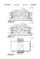
- FIG. 1An oblique view of a stacked three dimensional leadless semiconductor multiple chip module 10 comprising two semiconductor devices 11 each having a package body 12 on a PCB substrate 14 is illustrated in FIG. 1, a first embodiment of the present invention.
- the package body 12can be of but not limited to any conventional encapsulating material, for example, an epoxy resin-based molding compound.
- Package body 12can be formed either through overmolding or through a "glob top” process. Overmolding can be accomplished in a transfer mold, which is a common tool in the art.
- a "glob top” processis where an encapsulant is either dispensed or melted over a semiconductor die to cover it.
- PCB substrate 14has a plurality of metal conductors 16 extending past package body 12. Metal conductors 16 also extend to the bottom surface of PCB substrate 14.
- the advantage of semiconductor device 11 over conventional leaded packagesis that the problem of lead damage is eliminated because metal conductors 16 perform substantially the same function as the external leads of conventional semiconductor packages, but metal conductors 16 are supported by a PCB substrate 14.
- Semiconductor device 11can be tested and burned-in with a socket that makes contact with the plurality of metal conductors 16.
- metal conductors 16have semi-circular edges to form a plurality of half-vias 18 along the edges of PCB substrate 14 giving the edges a castellated appearance.
- the plurality of half-vias 18enables electrical interconnections between multiple semiconductor devices 11 to form a multiple chip module.
- Also illustrated in FIG. 1is a plurality of electrical conductors 22 that connect the two semiconductor devices 11.
- Electrical conductors 22can be either solder plated wires or solder filled springs.
- a solder filled springis basically a spring filled with solder that looks substantially like a solid column of solder. During solder reflow when the solder is melted, the coils of the spring prevent the solder from collapsing because the molten solder will wet to the spring due to surface tension.
- each semiconductor device 11has a semiconductor die 24 directly mounted to PCB substrate 14.
- Each semiconductor die 24is electrically connected to the plurality of metal conductors 16 by way of a plurality of wire bonds 26 as illustrated in FIG. 2.
- the wiresare bonded selectively to the plurality of metal conductors 16 so that each device in the stack is not identical. This differentiation is needed for chip enable requirements in the module. In some cases, the chip enable for each device is interconnected, but in that instance, the data outputs per device cannot be interconnected. Thus, it should be apparent that each device in the stack have to be marked accordingly because of the different wire bonding scheme of each device.
- the PCB substrates 14are positioned such that the plurality of half-vias 18 of both semiconductor devices 11 are aligned to each other in the X-Y direction.
- the plurality of electrical conductors 22fit into the plurality of half-vias 18 and are soldered thereto to electrically interconnect the semiconductor devices 11. Since each semiconductor device 11 is not identical in the wire bonding scheme, at least one of the plurality of electrical conductors 22 is unique per device. This uniqueness allows each device 11 to be selected during the multiple chip module's operation.
- the lower ends of the plurality of electrical conductors 22are bent to enable the semiconductor multiple chip module 10 to be surface mounted to a PC board (not shown).
- FIG. 2illustrates the plurality of electrical conductors 22 being bent outward, it is possible to bend the plurality of electrical conductors 22 inward and still enable surface mounting.
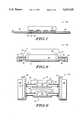
- FIG. 3illustrates a second embodiment of the present invention.
- Semiconductor multiple chip module 27has the same type of components as the module 10 of FIG. 2, and are thus labeled accordingly. The difference with the multiple chip module 27 is that the plurality of electrical conductors 23 in the form of solder filled springs; 22 are left straight to make the module 27 a through-hole type of module, as opposed to the surface mounting configuration of module 10 of FIG. 2.
- an alternative method for chip enableis offered if each device in the multiple chip module stack is desired to be wire bonded and marked identically.
- the chip enable connection for each devicecan be sheathed with an electrical insulator in such a manner that no electrical contact is made with the other device.
- chip enable for each devicecan be achieved.
- FIG. 4illustrates yet a third embodiment of the present invention.
- semiconductor multiple chip module 28has substantially the same type of components as the module 10 of FIG. 2, thus, the components are labeled the same where applicable.
- the plurality of electrical conductorsconsists of solder balls 29 attached to the bottom surface of substrate 14 of the upper device, solder balls 30 attached to the upper surface of substrate 14 of the lower device, and solder balls 31 attached to the bottom surface of substrate 14 of the lower device.
- solder balls 29 and 30are reflowed together, they form rigid interconnections between the upper and lower semiconductor devices 11 in the stack.
- the module 28can be surface mounted to a PC board 32 by reflowing the plurality of solder balls 31 to solder pads 33 on the PC board 32.
- FIG. 5illustrates a fourth embodiment of the present invention, having substantially the same components as semiconductor multiple chip module 28 of FIG. 4. Therefore, the components are labeled the same where applicable.
- Semiconductor multiple chip module 34has a single layer of solder balls 35 to interconnect the upper and lower semiconductor devices 11. This configuration is possible when the diameter of the solder ball 35 is greater than the height of package body 12.
- FIG. 6Illustrated in FIG. 6 is a top view of a semiconductor device 36 that has an overmolded package body 37 on a flexible substrate 38, a fifth embodiment of the present invention.
- the overmolded package body 37can be of but not limited to any conventional encapsulating material, for example, an epoxy resin-based molding compound.
- Flexible substrate 38has a plurality of metal conductors 40 on two opposing sides extending past the package body 37 to the edges of flexible substrate 38.
- Metal conductors 40are semi-circular in shape at the edges of the flexible substrate 38 to form a plurality of half-vias 42, giving those edges of the flexible substrate 38 a castellated appearance.
- metal conductors 40also extend from the top surface of flexible substrate 38 to the bottom surface of flexible substrate 38.
- the plurality of half-vias 42enables electrical interconnections between multiple semiconductor devices 36. Each semiconductor device 36 may be tested and burned-in individually.
- FIG. 6Additionally illustrated in FIG. 6 is a pair of thermally conductive extensions 44 which is an integral part of the flexible substrate 38.
- FIG. 7is an end view of the semiconductor device 36 further illustrating the pair of thermally conductive extensions 44.
- the thermally conductive extensions 44are actually continuous under the package body 37.
- a thermally conductive materialsuch as copper can be used for these extensions.
- the metal conductors 42need to be electrically isolated from this continuous pair of extensions.
- FIG. 8.is a cross-sectional view along line A--A of FIG. 6, illustrating how the continuous pair of thermal extensions 44 can be isolated from the metal conductors 40.
- a layer of electrical insulator 45is placed between the metal conductors 40 and the continuous pair of thermal extensions 44.
- FIG. 9illustrates a sixth embodiment of the present invention showing a multiple chip module 50 composed of two semiconductor devices 36 of FIG. 6.
- the two devices 36each having a semiconductor die 46 electrically coupled to the flexible substrate 38 with a plurality of wire bonds 47, are stacked above one another in a carrier socket 56 that is electrically nonconductive.
- Carrier socket 56can be molded from a thermally conductive molding compound, for example, an aluminum nitride filled molding compound.
- carrier socket 56has a plurality of spring contacts 58 which are electrical conductors to electrically interconnect the semiconductor devices 36.
- the plurality of spring contacts 58is pre-molded into carrier socket 56.
- the two semiconductor devices 36are self-aligning in carrier socket 56 because of the plurality of half-vias 42 formed by the metal conductors 40.
- the plurality of spring contacts 58fits into the plurality of half-vias and is soldered into place, or an external clip (not shown) can be used to hold the spring contacts 58 in contact with the metal conductors 40.
- the multiple chip module 50can be surface mounted to a PC board (not shown). It should be understood that each semiconductor device in the stack must be wire bonded differently and marked accordingly for either chip enable requirements or for separating data outputs per device.
- FIG. 10illustrates seventh embodiment of the present invention, which allows a different chip enable scheme.
- a semiconductor multiple chip module 60has substantially the same components as module 50 of FIG. 9, thus, the components are labeled the same where appropriate.
- a plurality of spring contacts(not fully shown) electrically interconnect the semiconductor devices 36.
- One spring contact 61makes a physical and electrical connection with only the upper device, while another spring contact 62 makes a physical and electrical contact with only the lower device. This configuration allows spring contacts 61 and 62 to be used for chip enable. The remaining spring contacts connect to both the upper and lower semiconductor devices.
- FIG. 11illustrates an end view of the multiple chip module 50.
- the end view for the multiple chip module 60 of FIG. 10will look substantially the same.
- the pairs of thermally conductive extensions 44are shown to touch the inner sidewalls of carrier socket 56.
- the flexibility of substrate 38enables the pair of thermally conductive extensions 44 to be bent in such a manner.
- This configurationsserves two purposes, the first one being an enhancement in the heat dissipation of the module 50.
- the bending of the pairs of thermally conductive extensions 44also help to hold each semiconductor device 36 in carrier socket 56 before the plurality of spring contacts 58 are soldered into place, due to the outward force that the extensions 44 exert on the sidewalls of carrier socket 56.
- FIG. 12Illustrated in FIG. 12 is a partial top view 64 of carrier socket 56 with the plurality of spring contacts 58, further illustrating the method for stacking multiple semiconductor devices in a carrier socket 56 using the plurality of half-vias 42 as the self-aligning feature.
- the inner sidewalls of carrier socket 56 that contain the plurality of spring contacts 58are castellated to prevent the plurality of spring contacts 58 from bending and shifting positions inside the socket 56.
- the plurality of spring contacts 58fits into the plurality of half-vias 42 of the semiconductor device as each device is pushed inside carrier socket 56.
- the locations of the plurality of spring contacts 58 and the plurality of half-vias 42ensure that each semiconductor device is properly self-aligned in the carrier socket 56.
- the foregoing description and illustrations contained hereindemonstrate many of the advantages associated with the present invention.
- the inventionenables three dimensional multiple chip module that can be surface mounted to a PC board.
- Three dimensional packagingoffers higher memory density and less required interconnect density than planar multiple chip substrates.
- the configuration of this three dimensional stacked leadless multiple chip moduleis self-aligning.
- the plurality of half-vias along the castellated edges of the substrateenables the simple stacking of semiconductor devices.
- the fact that each substrate can be directly stacked on top of another device without any additional layershelps to minimize the overall height of the multiple chip module.
- the plurality of electrical conductorsalso aid in the heat dissipation of the module.
Landscapes
- Engineering & Computer Science (AREA)
- Microelectronics & Electronic Packaging (AREA)
- Power Engineering (AREA)
- Physics & Mathematics (AREA)
- Condensed Matter Physics & Semiconductors (AREA)
- General Physics & Mathematics (AREA)
- Computer Hardware Design (AREA)
- Thermal Sciences (AREA)
- Lead Frames For Integrated Circuits (AREA)
- Cooling Or The Like Of Semiconductors Or Solid State Devices (AREA)
- Combinations Of Printed Boards (AREA)
- Connecting Device With Holders (AREA)
Abstract
Description
Claims (12)
Priority Applications (5)
| Application Number | Priority Date | Filing Date | Title |
|---|---|---|---|
| US07/887,963US5247423A (en) | 1992-05-26 | 1992-05-26 | Stacking three dimensional leadless multi-chip module and method for making the same |
| EP93105802AEP0571749A1 (en) | 1992-05-26 | 1993-04-08 | Stacking semiconductor multi-chip module and method for making the same |
| EP98106232AEP0862217A3 (en) | 1992-05-26 | 1993-04-08 | Semiconductor device and semiconductor multi-chip module |
| KR1019930008183AKR930024134A (en) | 1992-05-26 | 1993-05-13 | Multilayer semiconductor multi-chip module and manufacturing method thereof |
| JP5141266AJPH0637248A (en) | 1992-05-26 | 1993-05-21 | Stacked semiconductor multichip module and its manufacture |
Applications Claiming Priority (1)
| Application Number | Priority Date | Filing Date | Title |
|---|---|---|---|
| US07/887,963US5247423A (en) | 1992-05-26 | 1992-05-26 | Stacking three dimensional leadless multi-chip module and method for making the same |
Publications (1)
| Publication Number | Publication Date |
|---|---|
| US5247423Atrue US5247423A (en) | 1993-09-21 |
Family
ID=25392232
Family Applications (1)
| Application Number | Title | Priority Date | Filing Date |
|---|---|---|---|
| US07/887,963Expired - LifetimeUS5247423A (en) | 1992-05-26 | 1992-05-26 | Stacking three dimensional leadless multi-chip module and method for making the same |
Country Status (4)
| Country | Link |
|---|---|
| US (1) | US5247423A (en) |
| EP (2) | EP0571749A1 (en) |
| JP (1) | JPH0637248A (en) |
| KR (1) | KR930024134A (en) |
Cited By (164)
| Publication number | Priority date | Publication date | Assignee | Title |
|---|---|---|---|---|
| US5400218A (en)* | 1992-03-10 | 1995-03-21 | Thomson-Csf | Device for the 3D encapsulation of semiconductor chips |
| US5412159A (en)* | 1993-09-27 | 1995-05-02 | Zenith Electronics Corporation | High voltage resistive network circuit board with good potting adhesion |
| US5434745A (en)* | 1994-07-26 | 1995-07-18 | White Microelectronics Div. Of Bowmar Instrument Corp. | Stacked silicon die carrier assembly |
| US5544174A (en)* | 1994-03-17 | 1996-08-06 | The United States Of America As Represented By The Secretary Of The Air Force | Programmable boundary scan and input output parameter device for testing integrated circuits |
| US5561591A (en)* | 1990-08-01 | 1996-10-01 | Staktek Corporation | Multi-signal rail assembly with impedance control for a three-dimensional high density integrated circuit package |
| US5600541A (en)* | 1993-12-08 | 1997-02-04 | Hughes Aircraft Company | Vertical IC chip stack with discrete chip carriers formed from dielectric tape |
| US5623160A (en)* | 1995-09-14 | 1997-04-22 | Liberkowski; Janusz B. | Signal-routing or interconnect substrate, structure and apparatus |
| US5657206A (en)* | 1994-06-23 | 1997-08-12 | Cubic Memory, Inc. | Conductive epoxy flip-chip package and method |
| US5661087A (en)* | 1994-06-23 | 1997-08-26 | Cubic Memory, Inc. | Vertical interconnect process for silicon segments |
| US5661337A (en)* | 1995-11-07 | 1997-08-26 | Vlsi Technology, Inc. | Technique for improving bonding strength of leadframe to substrate in semiconductor IC chip packages |
| US5671121A (en)* | 1994-09-29 | 1997-09-23 | Intel Corporation | Kangaroo multi-package interconnection concept |
| US5696030A (en)* | 1994-09-30 | 1997-12-09 | International Business Machines Corporation | Integrated circuit contacts having improved electromigration characteristics and fabrication methods therefor |
| US5698895A (en)* | 1994-06-23 | 1997-12-16 | Cubic Memory, Inc. | Silicon segment programming method and apparatus |
| US5706172A (en)* | 1995-08-16 | 1998-01-06 | Samsung Electronics Co., Ltd. | Stacked semiconductor package having supporting bars and a socket therefor |
| WO1998000868A1 (en)* | 1996-06-28 | 1998-01-08 | Pac Tech - Packaging Technologies Gmbh | Process for forming a spatial chip arrangement, and said spatial arrangement |
| US5715144A (en)* | 1994-12-30 | 1998-02-03 | International Business Machines Corporation | Multi-layer, multi-chip pyramid and circuit board structure |
| US5748452A (en)* | 1996-07-23 | 1998-05-05 | International Business Machines Corporation | Multi-electronic device package |
| US5861666A (en)* | 1995-08-30 | 1999-01-19 | Tessera, Inc. | Stacked chip assembly |
| US5891761A (en)* | 1994-06-23 | 1999-04-06 | Cubic Memory, Inc. | Method for forming vertical interconnect process for silicon segments with thermally conductive epoxy preform |
| US5907903A (en)* | 1996-05-24 | 1999-06-01 | International Business Machines Corporation | Multi-layer-multi-chip pyramid and circuit board structure and method of forming same |
| US5956233A (en)* | 1997-12-19 | 1999-09-21 | Texas Instruments Incorporated | High density single inline memory module |
| US5973392A (en)* | 1997-04-02 | 1999-10-26 | Nec Corporation | Stacked carrier three-dimensional memory module and semiconductor device using the same |
| KR100239703B1 (en)* | 1996-10-21 | 2000-01-15 | 김영환 | Three dimension semiconductor package and fabrication method thereof |
| US6025642A (en)* | 1995-08-17 | 2000-02-15 | Staktek Corporation | Ultra high density integrated circuit packages |
| US6034441A (en)* | 1997-11-26 | 2000-03-07 | Lucent Technologies, Inc. | Overcast semiconductor package |
| US6049123A (en)* | 1990-08-01 | 2000-04-11 | Staktek Corporation | Ultra high density integrated circuit packages |
| EP0999593A1 (en)* | 1998-11-06 | 2000-05-10 | Bull S.A. | Three-dimensional interconnection structure with a plurality of circuits to fabricate a multi-component housing |
| US6080596A (en)* | 1994-06-23 | 2000-06-27 | Cubic Memory Inc. | Method for forming vertical interconnect process for silicon segments with dielectric isolation |
| US6121676A (en)* | 1996-12-13 | 2000-09-19 | Tessera, Inc. | Stacked microelectronic assembly and method therefor |
| US6124633A (en)* | 1994-06-23 | 2000-09-26 | Cubic Memory | Vertical interconnect process for silicon segments with thermally conductive epoxy preform |
| US6172423B1 (en)* | 1997-11-15 | 2001-01-09 | Hyundai Electronics Industries Co., Ltd. | Layer-type ball grid array semiconductor package and fabrication method thereof |
| US6219240B1 (en)* | 1998-07-02 | 2001-04-17 | R-Amtech International, Inc. | Three-dimensional electronic module and a method of its fabrication and repair |
| US6236565B1 (en)* | 2000-06-15 | 2001-05-22 | Mark G. Gordon | Chip stack with active cooling system |
| US6249136B1 (en) | 1999-06-28 | 2001-06-19 | Advanced Micro Devices, Inc. | Bottom side C4 bumps for integrated circuits |
| US6255726B1 (en) | 1994-06-23 | 2001-07-03 | Cubic Memory, Inc. | Vertical interconnect process for silicon segments with dielectric isolation |
| US6278181B1 (en) | 1999-06-28 | 2001-08-21 | Advanced Micro Devices, Inc. | Stacked multi-chip modules using C4 interconnect technology having improved thermal management |
| US6339255B1 (en)* | 1998-10-24 | 2002-01-15 | Hyundai Electronics Industries Co., Ltd. | Stacked semiconductor chips in a single semiconductor package |
| US6417027B1 (en) | 1999-06-10 | 2002-07-09 | Micron Technology, Inc. | High density stackable and flexible substrate-based devices and systems and methods of fabricating |
| US6462408B1 (en) | 2001-03-27 | 2002-10-08 | Staktek Group, L.P. | Contact member stacking system and method |
| CN1092399C (en)* | 1996-04-25 | 2002-10-09 | 东芝株式会社 | Method for manufacturing for semiconductor device |
| US6486528B1 (en) | 1994-06-23 | 2002-11-26 | Vertical Circuits, Inc. | Silicon segment programming apparatus and three terminal fuse configuration |
| US20030006496A1 (en)* | 2001-03-15 | 2003-01-09 | Venkateshwaran Vaiyapuri | Semiconductor/printed circuit board assembly, and computer system |
| US20030048624A1 (en)* | 2001-08-22 | 2003-03-13 | Tessera, Inc. | Low-height multi-component assemblies |
| US20030047353A1 (en)* | 2001-09-07 | 2003-03-13 | Yamaguchi James Satsuo | Multilayer modules with flexible substrates |
| US20030081392A1 (en)* | 2001-10-26 | 2003-05-01 | Staktek Group, L.P. | Integrated circuit stacking system and method |
| US6572387B2 (en) | 1999-09-24 | 2003-06-03 | Staktek Group, L.P. | Flexible circuit connector for stacked chip module |
| US6576992B1 (en) | 2001-10-26 | 2003-06-10 | Staktek Group L.P. | Chip scale stacking system and method |
| US20030107118A1 (en)* | 2001-10-09 | 2003-06-12 | Tessera, Inc. | Stacked packages |
| US20030131472A1 (en)* | 2002-01-15 | 2003-07-17 | Mitac International Corp. | Method of fabricating a multi-layer circuit board assembly |
| US6608763B1 (en) | 2000-09-15 | 2003-08-19 | Staktek Group L.P. | Stacking system and method |
| US20030168725A1 (en)* | 1996-12-13 | 2003-09-11 | Tessera, Inc. | Methods of making microelectronic assemblies including folded substrates |
| US6621155B1 (en) | 1999-12-23 | 2003-09-16 | Rambus Inc. | Integrated circuit device having stacked dies and impedance balanced transmission lines |
| US20040031972A1 (en)* | 2001-10-09 | 2004-02-19 | Tessera, Inc. | Stacked packages |
| US6699730B2 (en) | 1996-12-13 | 2004-03-02 | Tessers, Inc. | Stacked microelectronic assembly and method therefor |
| US20040045158A1 (en)* | 2000-02-08 | 2004-03-11 | Cardiac Pacemakers, Inc. | Thin film deposition as an active conductor and method therefor |
| US20040099938A1 (en)* | 2002-09-11 | 2004-05-27 | Tessera, Inc. | Assemblies having stacked semiconductor chips and methods of making same |
| US20040104470A1 (en)* | 2002-08-16 | 2004-06-03 | Tessera, Inc. | Microelectronic packages with self-aligning features |
| US6765288B2 (en) | 2002-08-05 | 2004-07-20 | Tessera, Inc. | Microelectronic adaptors, assemblies and methods |
| US20040183183A1 (en)* | 2001-10-26 | 2004-09-23 | Staktek Group, L.P. | Integrated circuit stacking system and method |
| US20040191442A1 (en)* | 2003-03-27 | 2004-09-30 | Florencia Lim | Surface modification of expanded ultra high molecular weight polyethylene (eUHMWPE) for improved bondability |
| US20040229403A1 (en)* | 2001-03-30 | 2004-11-18 | Salman Akram | Die stacking scheme |
| US20040262777A1 (en)* | 2002-10-11 | 2004-12-30 | Tessera, Inc. | Components, methods and assemblies for multi-chip packages |
| US6885106B1 (en) | 2001-01-11 | 2005-04-26 | Tessera, Inc. | Stacked microelectronic assemblies and methods of making same |
| US6890798B2 (en) | 1999-06-08 | 2005-05-10 | Intel Corporation | Stacked chip packaging |
| US6914324B2 (en) | 2001-10-26 | 2005-07-05 | Staktek Group L.P. | Memory expansion and chip scale stacking system and method |
| US6919626B2 (en) | 1992-12-11 | 2005-07-19 | Staktek Group L.P. | High density integrated circuit module |
| US20050167817A1 (en)* | 2002-08-05 | 2005-08-04 | Tessera, Inc. | Microelectronic adaptors, assemblies and methods |
| US20050189623A1 (en)* | 2001-03-12 | 2005-09-01 | Salman Akram | Multiple die package |
| US20050224952A1 (en)* | 2004-04-13 | 2005-10-13 | Al Vindasius | Three dimensional six surface conformal die coating |
| US20050258530A1 (en)* | 2004-04-13 | 2005-11-24 | Al Vindasius | Micropede stacked die component assembly |
| US20060000638A1 (en)* | 2004-06-30 | 2006-01-05 | Honeywell International Inc. | Micro-castellated interposer |
| DE19709259B4 (en)* | 1996-03-06 | 2006-02-23 | Hyundai Electronics Industries Co., Ltd., Ichon | Multi-layer ground connection housing |
| US7026708B2 (en) | 2001-10-26 | 2006-04-11 | Staktek Group L.P. | Low profile chip scale stacking system and method |
| US7033861B1 (en) | 2005-05-18 | 2006-04-25 | Staktek Group L.P. | Stacked module systems and method |
| US7053478B2 (en) | 2001-10-26 | 2006-05-30 | Staktek Group L.P. | Pitch change and chip scale stacking system |
| US7081373B2 (en) | 2001-12-14 | 2006-07-25 | Staktek Group, L.P. | CSP chip stack with flex circuit |
| US7098073B1 (en) | 2005-04-18 | 2006-08-29 | Freescale Semiconductor, Inc. | Method for stacking an integrated circuit on another integrated circuit |
| US20060231938A1 (en)* | 2005-04-18 | 2006-10-19 | Mangrum Marc A | Structure for stacking an integrated circuit on another integrated circuit |
| US7180167B2 (en) | 2001-10-26 | 2007-02-20 | Staktek Group L. P. | Low profile stacking system and method |
| US7202555B2 (en) | 2001-10-26 | 2007-04-10 | Staktek Group L.P. | Pitch change and chip scale stacking system and method |
| US7215018B2 (en) | 2004-04-13 | 2007-05-08 | Vertical Circuits, Inc. | Stacked die BGA or LGA component assembly |
| US7217597B2 (en) | 2004-06-22 | 2007-05-15 | Micron Technology, Inc. | Die stacking scheme |
| USRE39628E1 (en) | 1999-05-05 | 2007-05-15 | Stakick Group, L.P. | Stackable flex circuit IC package and method of making same |
| US20070115645A1 (en)* | 2001-08-17 | 2007-05-24 | Jacobsen Jeffrey J | Apparatuses and methods for forming wireless RF labels |
| US20070136766A1 (en)* | 2005-12-09 | 2007-06-14 | Ryuichi Iwamura | Cross-phase adapter for powerline communications (PLC) network |
| US20070155053A1 (en)* | 2002-09-17 | 2007-07-05 | Chippac, Inc. | Semiconductor Multi-Package Module Having Package Stacked Over Ball Grid Array Package and Having Wire Bond Interconnect Between Stacked Packages |
| EP1318546A4 (en)* | 2000-07-19 | 2007-08-08 | Shindo Company Ltd | Semiconductor device |
| CN100343964C (en)* | 2004-02-13 | 2007-10-17 | 旺宏电子股份有限公司 | Multi-chip package structure |
| US7289327B2 (en) | 2006-02-27 | 2007-10-30 | Stakick Group L.P. | Active cooling methods and apparatus for modules |
| US7304382B2 (en) | 2006-01-11 | 2007-12-04 | Staktek Group L.P. | Managed memory component |
| US20070278660A1 (en)* | 2006-05-30 | 2007-12-06 | Stats Chippac Ltd. | Integrated circuit package system with edge connection system |
| US7310458B2 (en) | 2001-10-26 | 2007-12-18 | Staktek Group L.P. | Stacked module systems and methods |
| US7309914B2 (en) | 2005-01-20 | 2007-12-18 | Staktek Group L.P. | Inverted CSP stacking system and method |
| US20070292990A1 (en)* | 2002-09-17 | 2007-12-20 | Marcos Karnezos | Semiconductor multi-package module having wire bond interconnect between stacked packages |
| US20080003402A1 (en)* | 2003-10-06 | 2008-01-03 | Tessera, Inc. | Fine pitch microcontacts and method for forming thereof |
| US7324352B2 (en) | 2004-09-03 | 2008-01-29 | Staktek Group L.P. | High capacity thin module system and method |
| US20080036096A1 (en)* | 2002-09-17 | 2008-02-14 | Marcos Karnezos | Semiconductor Multi-Package Module Having Package Stacked Over Die-Up Flip Chip Ball Grid Array Package and Having Wire Bond Interconnect Between Stacked Packages |
| US20080042274A1 (en)* | 2002-09-06 | 2008-02-21 | Tessera, Inc. | Components, methods and assemblies for stacked packages |
| US7335995B2 (en) | 2001-10-09 | 2008-02-26 | Tessera, Inc. | Microelectronic assembly having array including passive elements and interconnects |
| KR100817054B1 (en) | 2006-07-13 | 2008-03-26 | 삼성전자주식회사 | Socket for package test, rubber for test socket and guide for test socket |
| US7371609B2 (en) | 2001-10-26 | 2008-05-13 | Staktek Group L.P. | Stacked module systems and methods |
| WO2008021575A3 (en)* | 2006-08-16 | 2008-07-10 | Tessera Inc | Microelectronic package |
| US7417310B2 (en) | 2006-11-02 | 2008-08-26 | Entorian Technologies, Lp | Circuit module having force resistant construction |
| US7423885B2 (en) | 2004-09-03 | 2008-09-09 | Entorian Technologies, Lp | Die module system |
| US7443023B2 (en) | 2004-09-03 | 2008-10-28 | Entorian Technologies, Lp | High capacity thin module system |
| US7446410B2 (en) | 2004-09-03 | 2008-11-04 | Entorian Technologies, Lp | Circuit module with thermal casing systems |
| US7468893B2 (en) | 2004-09-03 | 2008-12-23 | Entorian Technologies, Lp | Thin module system and method |
| US7468553B2 (en) | 2006-10-20 | 2008-12-23 | Entorian Technologies, Lp | Stackable micropackages and stacked modules |
| US20090008795A1 (en)* | 2007-07-02 | 2009-01-08 | Tessera, Inc. | Stackable microelectronic device carriers, stacked device carriers and methods of making the same |
| WO2009003791A1 (en)* | 2007-06-30 | 2009-01-08 | Robert Bosch Gmbh | Electronic module and method for producing an electronic module |
| US7480152B2 (en) | 2004-09-03 | 2009-01-20 | Entorian Technologies, Lp | Thin module system and method |
| US7485951B2 (en) | 2001-10-26 | 2009-02-03 | Entorian Technologies, Lp | Modularized die stacking system and method |
| US7508069B2 (en) | 2006-01-11 | 2009-03-24 | Entorian Technologies, Lp | Managed memory component |
| US7508058B2 (en) | 2006-01-11 | 2009-03-24 | Entorian Technologies, Lp | Stacked integrated circuit module |
| US7511969B2 (en) | 2006-02-02 | 2009-03-31 | Entorian Technologies, Lp | Composite core circuit module system and method |
| US7511968B2 (en) | 2004-09-03 | 2009-03-31 | Entorian Technologies, Lp | Buffered thin module system and method |
| US7522421B2 (en) | 2004-09-03 | 2009-04-21 | Entorian Technologies, Lp | Split core circuit module |
| US7542297B2 (en) | 2004-09-03 | 2009-06-02 | Entorian Technologies, Lp | Optimized mounting area circuit module system and method |
| US7542304B2 (en) | 2003-09-15 | 2009-06-02 | Entorian Technologies, Lp | Memory expansion and integrated circuit stacking system and method |
| US7545029B2 (en) | 2006-08-18 | 2009-06-09 | Tessera, Inc. | Stack microelectronic assemblies |
| US20090179318A1 (en)* | 2008-01-10 | 2009-07-16 | Abounion Technology Corporation | Multi-channel stackable semiconductor device and method for fabricating the same, and stacking substrate applied to the semiconductor device |
| US7576995B2 (en) | 2005-11-04 | 2009-08-18 | Entorian Technologies, Lp | Flex circuit apparatus and method for adding capacitance while conserving circuit board surface area |
| US7579687B2 (en) | 2004-09-03 | 2009-08-25 | Entorian Technologies, Lp | Circuit module turbulence enhancement systems and methods |
| US7606049B2 (en) | 2004-09-03 | 2009-10-20 | Entorian Technologies, Lp | Module thermal management system and method |
| US7606040B2 (en) | 2004-09-03 | 2009-10-20 | Entorian Technologies, Lp | Memory module system and method |
| US7606050B2 (en) | 2004-09-03 | 2009-10-20 | Entorian Technologies, Lp | Compact module system and method |
| US7605454B2 (en) | 2006-01-11 | 2009-10-20 | Entorian Technologies, Lp | Memory card and method for devising |
| US7608920B2 (en) | 2006-01-11 | 2009-10-27 | Entorian Technologies, Lp | Memory card and method for devising |
| US7616452B2 (en) | 2004-09-03 | 2009-11-10 | Entorian Technologies, Lp | Flex circuit constructions for high capacity circuit module systems and methods |
| USRE41039E1 (en) | 2000-01-13 | 2009-12-15 | Entorian Technologies, Lp | Stackable chip package with flex carrier |
| US7656678B2 (en) | 2001-10-26 | 2010-02-02 | Entorian Technologies, Lp | Stacked module systems |
| EP1547141A4 (en)* | 2002-09-17 | 2010-02-24 | Chippac Inc | Semiconductor multi-package module having wire bond interconnection between stacked packages |
| US7719098B2 (en) | 2001-10-26 | 2010-05-18 | Entorian Technologies Lp | Stacked modules and method |
| US7760513B2 (en) | 2004-09-03 | 2010-07-20 | Entorian Technologies Lp | Modified core for circuit module system and method |
| US20100193970A1 (en)* | 2003-12-30 | 2010-08-05 | Tessera, Inc. | Micro pin grid array with pin motion isolation |
| US8299626B2 (en) | 2007-08-16 | 2012-10-30 | Tessera, Inc. | Microelectronic package |
| USD680119S1 (en)* | 2011-11-15 | 2013-04-16 | Connectblue Ab | Module |
| USD680545S1 (en)* | 2011-11-15 | 2013-04-23 | Connectblue Ab | Module |
| USD689053S1 (en)* | 2011-11-15 | 2013-09-03 | Connectblue Ab | Module |
| USD692896S1 (en)* | 2011-11-15 | 2013-11-05 | Connectblue Ab | Module |
| US8580607B2 (en) | 2010-07-27 | 2013-11-12 | Tessera, Inc. | Microelectronic packages with nanoparticle joining |
| US8604348B2 (en) | 2003-10-06 | 2013-12-10 | Tessera, Inc. | Method of making a connection component with posts and pads |
| US8611090B2 (en)* | 2010-09-09 | 2013-12-17 | International Business Machines Corporation | Electronic module with laterally-conducting heat distributor layer |
| US8698288B1 (en)* | 2013-05-23 | 2014-04-15 | Freescale Semiconductor, Inc. | Flexible substrate with crimping interconnection |
| US8723318B2 (en) | 2010-07-08 | 2014-05-13 | Tessera, Inc. | Microelectronic packages with dual or multiple-etched flip-chip connectors |
| US8779585B2 (en) | 2011-08-05 | 2014-07-15 | International Business Machines Corporation | Implementing enhanced thermal conductivity in stacked modules |
| US20140197541A1 (en)* | 2013-01-15 | 2014-07-17 | Freescale Semiconductor, Inc. | Microelectronic assembly having a heat spreader for a plurality of die |
| US8853558B2 (en) | 2010-12-10 | 2014-10-07 | Tessera, Inc. | Interconnect structure |
| US8872318B2 (en) | 2011-08-24 | 2014-10-28 | Tessera, Inc. | Through interposer wire bond using low CTE interposer with coarse slot apertures |
| US8884420B1 (en)* | 2013-07-12 | 2014-11-11 | Infineon Technologies Austria Ag | Multichip device |
| US8884448B2 (en) | 2007-09-28 | 2014-11-11 | Tessera, Inc. | Flip chip interconnection with double post |
| USRE45463E1 (en) | 2003-11-12 | 2015-04-14 | Tessera, Inc. | Stacked microelectronic assemblies with central contacts |
| US9171742B2 (en) | 2013-07-22 | 2015-10-27 | Globalfoundries U.S. 2 Llc | Alignment of integrated circuit chip stack |
| US20170005022A1 (en)* | 2014-01-26 | 2017-01-05 | Tsinghua University | Packaging structure, packaging method and template used in packaging method |
| US9633971B2 (en) | 2015-07-10 | 2017-04-25 | Invensas Corporation | Structures and methods for low temperature bonding using nanoparticles |
| US10380016B2 (en)* | 2017-03-01 | 2019-08-13 | Toshiba Memory Corporation | Semiconductor device including one or more semiconductor chips on a substrate |
| US10535626B2 (en) | 2015-07-10 | 2020-01-14 | Invensas Corporation | Structures and methods for low temperature bonding using nanoparticles |
| US20200253060A1 (en)* | 2011-05-11 | 2020-08-06 | Vlt, Inc. | Panel-molded electronic assemblies |
| CN112349705A (en)* | 2019-08-08 | 2021-02-09 | 南茂科技股份有限公司 | Electronic packaging device |
| US11973056B2 (en) | 2016-10-27 | 2024-04-30 | Adeia Semiconductor Technologies Llc | Methods for low temperature bonding using nanoparticles |
| US12096549B1 (en) | 2015-06-04 | 2024-09-17 | Vicor Corporation | Panel molded electronic assemblies with multi-surface conductive contacts |
| US12108129B2 (en)* | 2019-10-23 | 2024-10-01 | Canon Kabushiki Kaisha | Imaging apparatus, and moving object |
| US12200862B1 (en) | 2018-12-12 | 2025-01-14 | Vicor Corporation | Panel molded electronic assemblies with integral terminals |
| US12211809B2 (en) | 2020-12-30 | 2025-01-28 | Adeia Semiconductor Bonding Technologies Inc. | Structure with conductive feature and method of forming same |
Families Citing this family (22)
| Publication number | Priority date | Publication date | Assignee | Title |
|---|---|---|---|---|
| JP2944449B2 (en)* | 1995-02-24 | 1999-09-06 | 日本電気株式会社 | Semiconductor package and manufacturing method thereof |
| JPH0969587A (en)* | 1995-08-30 | 1997-03-11 | Nec Kyushu Ltd | Bga type semiconductor device and bga module |
| KR100192179B1 (en)* | 1996-03-06 | 1999-06-15 | 김영환 | Semiconductor package |
| DE19638175C2 (en) | 1996-09-18 | 2000-05-25 | Siemens Ag | Integrated circuit (chip) with a housing and external configuration option |
| KR100422608B1 (en)* | 1997-05-10 | 2004-06-04 | 삼성전자주식회사 | Stack chip package |
| KR20000050605A (en)* | 1999-01-12 | 2000-08-05 | 박천주 | Solderless and Wireless Socket-type Circuit Board pressed and adhered with multi-layered conductible circuit panel |
| KR100530911B1 (en)* | 1999-10-01 | 2005-11-23 | 세이코 엡슨 가부시키가이샤 | Wiring board, semiconductor device and method of producing, testing and packaging the same, and circuit board and electronic equipment |
| KR100675728B1 (en)* | 2000-03-16 | 2007-02-01 | 삼성전자주식회사 | Laminated chip package |
| KR20010086476A (en)* | 2001-07-13 | 2001-09-13 | 신이술 | Printed circuit board and package method of stacking semiconductor using therof |
| DE10134648A1 (en)* | 2001-07-20 | 2002-10-10 | Infineon Technologies Ag | Stacked electronic component device has perpendicular pins providing mechanical and electrical connections between stacked electronic components |
| JP2003318361A (en)* | 2002-04-19 | 2003-11-07 | Fujitsu Ltd | Semiconductor device and method of manufacturing the same |
| US7134194B2 (en) | 2003-11-13 | 2006-11-14 | Delphi Technologies, Inc. | Method of developing an electronic module |
| DE102004044882B3 (en)* | 2004-09-14 | 2006-04-20 | Infineon Technologies Ag | Semiconductor module having stacked semiconductor devices and electrical interconnects between the stacked semiconductor devices |
| KR100658734B1 (en)* | 2004-11-11 | 2006-12-19 | 주식회사 유니세미콘 | A stack semiconductor package and its manufacture method |
| US7483561B2 (en)* | 2004-11-30 | 2009-01-27 | Psion Teklogix Systems Inc. | Miniaturized imaging module construction technique |
| US7967184B2 (en) | 2005-11-16 | 2011-06-28 | Sandisk Corporation | Padless substrate for surface mounted components |
| KR101330731B1 (en)* | 2007-02-08 | 2013-11-20 | 삼성전자주식회사 | Image forming apparatus |
| US7906838B2 (en)* | 2007-07-23 | 2011-03-15 | Headway Technologies, Inc. | Electronic component package and method of manufacturing same |
| TWI399845B (en)* | 2009-09-24 | 2013-06-21 | Powertech Technology Inc | Multi-chip stacked device without loop height and its manufacturing method |
| KR101772490B1 (en) | 2011-09-28 | 2017-08-30 | 삼성전자주식회사 | Printed circuit board assembly |
| KR102158785B1 (en)* | 2018-12-14 | 2020-09-22 | 국방과학연구소 | Laser diode bar structure and package of stacked laser diode bar |
| KR102398110B1 (en)* | 2020-08-13 | 2022-05-13 | 주식회사 경신 | In-cable controller of charger |
Citations (7)
| Publication number | Priority date | Publication date | Assignee | Title |
|---|---|---|---|---|
| US3304468A (en)* | 1965-05-05 | 1967-02-14 | Gen Electric | Replaceable electronic module for master circuit boards |
| US3428954A (en)* | 1965-04-02 | 1969-02-18 | Ind Bull General Electric Sa S | Element for resistive permanent memory |
| US3588852A (en)* | 1967-12-26 | 1971-06-28 | Cambridge Memory Systems Inc | Memory assembly |
| US4956694A (en)* | 1988-11-04 | 1990-09-11 | Dense-Pac Microsystems, Inc. | Integrated circuit chip stacking |
| US5016138A (en)* | 1987-10-27 | 1991-05-14 | Woodman John K | Three dimensional integrated circuit package |
| US5155661A (en)* | 1991-05-15 | 1992-10-13 | Hewlett-Packard Company | Aluminum nitride multi-chip module |
| US5162975A (en)* | 1991-10-15 | 1992-11-10 | Hewlett-Packard Company | Integrated circuit demountable TAB apparatus |
Family Cites Families (5)
| Publication number | Priority date | Publication date | Assignee | Title |
|---|---|---|---|---|
| US3550766A (en)* | 1969-03-03 | 1970-12-29 | David Nixen | Flat electronic package assembly |
| JPS61101067A (en)* | 1984-10-24 | 1986-05-19 | Nec Corp | Memory module |
| JPH0773117B2 (en)* | 1986-11-25 | 1995-08-02 | 株式会社東芝 | Semiconductor package |
| US4862249A (en)* | 1987-04-17 | 1989-08-29 | Xoc Devices, Inc. | Packaging system for stacking integrated circuits |
| EP0509065A1 (en)* | 1990-08-01 | 1992-10-21 | Staktek Corporation | Ultra high density integrated circuit packages, method and apparatus |
- 1992
- 1992-05-26USUS07/887,963patent/US5247423A/ennot_activeExpired - Lifetime
- 1993
- 1993-04-08EPEP93105802Apatent/EP0571749A1/ennot_activeWithdrawn
- 1993-04-08EPEP98106232Apatent/EP0862217A3/ennot_activeWithdrawn
- 1993-05-13KRKR1019930008183Apatent/KR930024134A/ennot_activeCeased
- 1993-05-21JPJP5141266Apatent/JPH0637248A/enactivePending
Patent Citations (7)
| Publication number | Priority date | Publication date | Assignee | Title |
|---|---|---|---|---|
| US3428954A (en)* | 1965-04-02 | 1969-02-18 | Ind Bull General Electric Sa S | Element for resistive permanent memory |
| US3304468A (en)* | 1965-05-05 | 1967-02-14 | Gen Electric | Replaceable electronic module for master circuit boards |
| US3588852A (en)* | 1967-12-26 | 1971-06-28 | Cambridge Memory Systems Inc | Memory assembly |
| US5016138A (en)* | 1987-10-27 | 1991-05-14 | Woodman John K | Three dimensional integrated circuit package |
| US4956694A (en)* | 1988-11-04 | 1990-09-11 | Dense-Pac Microsystems, Inc. | Integrated circuit chip stacking |
| US5155661A (en)* | 1991-05-15 | 1992-10-13 | Hewlett-Packard Company | Aluminum nitride multi-chip module |
| US5162975A (en)* | 1991-10-15 | 1992-11-10 | Hewlett-Packard Company | Integrated circuit demountable TAB apparatus |
Non-Patent Citations (4)
| Title |
|---|
| "Large Capacity Memory Board Using Stacked Chip Assembly," by Kenzo Hatada et al., The Third Microelectronics Symposium (MES '89), Jul. 1989. |
| "Stacked High-Density Multichip Module," by R. A. Jarvela et al., IBM Technical Disclosure Bulletin, vol. 14, No. 10, Mar. 1972, pp. 2896-2897. |
| Large Capacity Memory Board Using Stacked Chip Assembly, by Kenzo Hatada et al., The Third Microelectronics Symposium (MES 89), Jul. 1989.* |
| Stacked High Density Multichip Module, by R. A. Jarvela et al., IBM Technical Disclosure Bulletin, vol. 14, No. 10, Mar. 1972, pp. 2896 2897.* |
Cited By (270)
| Publication number | Priority date | Publication date | Assignee | Title |
|---|---|---|---|---|
| US6049123A (en)* | 1990-08-01 | 2000-04-11 | Staktek Corporation | Ultra high density integrated circuit packages |
| US5561591A (en)* | 1990-08-01 | 1996-10-01 | Staktek Corporation | Multi-signal rail assembly with impedance control for a three-dimensional high density integrated circuit package |
| US6168970B1 (en) | 1990-08-01 | 2001-01-02 | Staktek Group L.P. | Ultra high density integrated circuit packages |
| US5400218A (en)* | 1992-03-10 | 1995-03-21 | Thomson-Csf | Device for the 3D encapsulation of semiconductor chips |
| US6919626B2 (en) | 1992-12-11 | 2005-07-19 | Staktek Group L.P. | High density integrated circuit module |
| US5412159A (en)* | 1993-09-27 | 1995-05-02 | Zenith Electronics Corporation | High voltage resistive network circuit board with good potting adhesion |
| US5600541A (en)* | 1993-12-08 | 1997-02-04 | Hughes Aircraft Company | Vertical IC chip stack with discrete chip carriers formed from dielectric tape |
| US5544174A (en)* | 1994-03-17 | 1996-08-06 | The United States Of America As Represented By The Secretary Of The Air Force | Programmable boundary scan and input output parameter device for testing integrated circuits |
| US5698895A (en)* | 1994-06-23 | 1997-12-16 | Cubic Memory, Inc. | Silicon segment programming method and apparatus |
| US6188126B1 (en) | 1994-06-23 | 2001-02-13 | Cubic Memory Inc. | Vertical interconnect process for silicon segments |
| US5994170A (en)* | 1994-06-23 | 1999-11-30 | Cubic Memory, Inc. | Silicon segment programming method |
| US5675180A (en)* | 1994-06-23 | 1997-10-07 | Cubic Memory, Inc. | Vertical interconnect process for silicon segments |
| US6255726B1 (en) | 1994-06-23 | 2001-07-03 | Cubic Memory, Inc. | Vertical interconnect process for silicon segments with dielectric isolation |
| US6124633A (en)* | 1994-06-23 | 2000-09-26 | Cubic Memory | Vertical interconnect process for silicon segments with thermally conductive epoxy preform |
| US5661087A (en)* | 1994-06-23 | 1997-08-26 | Cubic Memory, Inc. | Vertical interconnect process for silicon segments |
| US6080596A (en)* | 1994-06-23 | 2000-06-27 | Cubic Memory Inc. | Method for forming vertical interconnect process for silicon segments with dielectric isolation |
| US5657206A (en)* | 1994-06-23 | 1997-08-12 | Cubic Memory, Inc. | Conductive epoxy flip-chip package and method |
| US5891761A (en)* | 1994-06-23 | 1999-04-06 | Cubic Memory, Inc. | Method for forming vertical interconnect process for silicon segments with thermally conductive epoxy preform |
| US6486528B1 (en) | 1994-06-23 | 2002-11-26 | Vertical Circuits, Inc. | Silicon segment programming apparatus and three terminal fuse configuration |
| US5837566A (en)* | 1994-06-23 | 1998-11-17 | Cubic Memory, Inc. | Vertical interconnect process for silicon segments |
| US5434745A (en)* | 1994-07-26 | 1995-07-18 | White Microelectronics Div. Of Bowmar Instrument Corp. | Stacked silicon die carrier assembly |
| US5671121A (en)* | 1994-09-29 | 1997-09-23 | Intel Corporation | Kangaroo multi-package interconnection concept |
| US5760477A (en)* | 1994-09-30 | 1998-06-02 | International Business Machines Corporation | Integrated circuit contacts having resistive electromigration characteristics |
| US5696030A (en)* | 1994-09-30 | 1997-12-09 | International Business Machines Corporation | Integrated circuit contacts having improved electromigration characteristics and fabrication methods therefor |
| US5715144A (en)* | 1994-12-30 | 1998-02-03 | International Business Machines Corporation | Multi-layer, multi-chip pyramid and circuit board structure |
| US5706172A (en)* | 1995-08-16 | 1998-01-06 | Samsung Electronics Co., Ltd. | Stacked semiconductor package having supporting bars and a socket therefor |
| US6025642A (en)* | 1995-08-17 | 2000-02-15 | Staktek Corporation | Ultra high density integrated circuit packages |
| US5861666A (en)* | 1995-08-30 | 1999-01-19 | Tessera, Inc. | Stacked chip assembly |
| US5691209A (en)* | 1995-09-14 | 1997-11-25 | Liberkowski; Janusz B. | Lattice interconnect method and apparatus for manufacturing multi-chip modules |
| US5623160A (en)* | 1995-09-14 | 1997-04-22 | Liberkowski; Janusz B. | Signal-routing or interconnect substrate, structure and apparatus |
| US5661337A (en)* | 1995-11-07 | 1997-08-26 | Vlsi Technology, Inc. | Technique for improving bonding strength of leadframe to substrate in semiconductor IC chip packages |
| DE19709259B4 (en)* | 1996-03-06 | 2006-02-23 | Hyundai Electronics Industries Co., Ltd., Ichon | Multi-layer ground connection housing |
| CN1092399C (en)* | 1996-04-25 | 2002-10-09 | 东芝株式会社 | Method for manufacturing for semiconductor device |
| US5907903A (en)* | 1996-05-24 | 1999-06-01 | International Business Machines Corporation | Multi-layer-multi-chip pyramid and circuit board structure and method of forming same |
| US7087442B2 (en) | 1996-06-28 | 2006-08-08 | Pac Tech-Packaging Technologies Gmbh | Process for the formation of a spatial chip arrangement and spatial chip arrangement |
| US20020009828A1 (en)* | 1996-06-28 | 2002-01-24 | Pac Tech - Packaging Technologies Gmbh | Process for the formation of a spatial chip arrangement and spatial chip arrangement |
| WO1998000868A1 (en)* | 1996-06-28 | 1998-01-08 | Pac Tech - Packaging Technologies Gmbh | Process for forming a spatial chip arrangement, and said spatial arrangement |
| US6101100A (en)* | 1996-07-23 | 2000-08-08 | International Business Machines Corporation | Multi-electronic device package |
| KR100259450B1 (en)* | 1996-07-23 | 2000-06-15 | 포만 제프리 엘 | Multi-electronic device package |
| US5748452A (en)* | 1996-07-23 | 1998-05-05 | International Business Machines Corporation | Multi-electronic device package |
| KR100239703B1 (en)* | 1996-10-21 | 2000-01-15 | 김영환 | Three dimension semiconductor package and fabrication method thereof |
| US6121676A (en)* | 1996-12-13 | 2000-09-19 | Tessera, Inc. | Stacked microelectronic assembly and method therefor |
| US7149095B2 (en) | 1996-12-13 | 2006-12-12 | Tessera, Inc. | Stacked microelectronic assemblies |
| US6699730B2 (en) | 1996-12-13 | 2004-03-02 | Tessers, Inc. | Stacked microelectronic assembly and method therefor |
| US20030168725A1 (en)* | 1996-12-13 | 2003-09-11 | Tessera, Inc. | Methods of making microelectronic assemblies including folded substrates |
| US5973392A (en)* | 1997-04-02 | 1999-10-26 | Nec Corporation | Stacked carrier three-dimensional memory module and semiconductor device using the same |
| US6172423B1 (en)* | 1997-11-15 | 2001-01-09 | Hyundai Electronics Industries Co., Ltd. | Layer-type ball grid array semiconductor package and fabrication method thereof |
| US6034441A (en)* | 1997-11-26 | 2000-03-07 | Lucent Technologies, Inc. | Overcast semiconductor package |
| US5956233A (en)* | 1997-12-19 | 1999-09-21 | Texas Instruments Incorporated | High density single inline memory module |
| US6219240B1 (en)* | 1998-07-02 | 2001-04-17 | R-Amtech International, Inc. | Three-dimensional electronic module and a method of its fabrication and repair |
| US6339255B1 (en)* | 1998-10-24 | 2002-01-15 | Hyundai Electronics Industries Co., Ltd. | Stacked semiconductor chips in a single semiconductor package |
| US6500698B2 (en) | 1998-10-24 | 2002-12-31 | Hynix Semiconductor, Inc. | Method for fabricating a stacked semiconductor chip package |
| EP0999593A1 (en)* | 1998-11-06 | 2000-05-10 | Bull S.A. | Three-dimensional interconnection structure with a plurality of circuits to fabricate a multi-component housing |
| FR2785722A1 (en)* | 1998-11-06 | 2000-05-12 | Bull Sa | THREE-DIMENSIONAL INTERCONNECTION STRUCTURE OF MULTIPLE CIRCUITS TO FORM A MULTI-COMPONENT PACKAGE |
| USRE39628E1 (en) | 1999-05-05 | 2007-05-15 | Stakick Group, L.P. | Stackable flex circuit IC package and method of making same |
| US6890798B2 (en) | 1999-06-08 | 2005-05-10 | Intel Corporation | Stacked chip packaging |
| US6617671B1 (en)* | 1999-06-10 | 2003-09-09 | Micron Technology, Inc. | High density stackable and flexible substrate-based semiconductor device modules |
| US6785144B1 (en) | 1999-06-10 | 2004-08-31 | Micron Technology, Inc. | High density stackable and flexible substrate-based devices and systems and methods of fabricating |
| US6417027B1 (en) | 1999-06-10 | 2002-07-09 | Micron Technology, Inc. | High density stackable and flexible substrate-based devices and systems and methods of fabricating |
| US6249136B1 (en) | 1999-06-28 | 2001-06-19 | Advanced Micro Devices, Inc. | Bottom side C4 bumps for integrated circuits |
| US6278181B1 (en) | 1999-06-28 | 2001-08-21 | Advanced Micro Devices, Inc. | Stacked multi-chip modules using C4 interconnect technology having improved thermal management |
| US6572387B2 (en) | 1999-09-24 | 2003-06-03 | Staktek Group, L.P. | Flexible circuit connector for stacked chip module |
| US7066741B2 (en) | 1999-09-24 | 2006-06-27 | Staktek Group L.P. | Flexible circuit connector for stacked chip module |
| US6621155B1 (en) | 1999-12-23 | 2003-09-16 | Rambus Inc. | Integrated circuit device having stacked dies and impedance balanced transmission lines |
| USRE43720E1 (en) | 1999-12-23 | 2012-10-09 | Rambus Inc. | Integrated circuit device having stacked dies and impedance balanced transmission lines |
| USRE41039E1 (en) | 2000-01-13 | 2009-12-15 | Entorian Technologies, Lp | Stackable chip package with flex carrier |
| US7646614B2 (en) | 2000-02-08 | 2010-01-12 | Cardiac Pacemakers, Inc. | Thin film deposition as an active conductor and method therefor |
| US7375982B2 (en)* | 2000-02-08 | 2008-05-20 | Cardiac Pacemakers, Inc. | Thin film deposition as an active conductor and method therefor |
| US20040045158A1 (en)* | 2000-02-08 | 2004-03-11 | Cardiac Pacemakers, Inc. | Thin film deposition as an active conductor and method therefor |
| US20080218989A1 (en)* | 2000-02-08 | 2008-09-11 | Cardiac Pacemakers, Inc. | Thin film deposition as an active conductor and method therfor |
| US6236565B1 (en)* | 2000-06-15 | 2001-05-22 | Mark G. Gordon | Chip stack with active cooling system |
| EP1318546A4 (en)* | 2000-07-19 | 2007-08-08 | Shindo Company Ltd | Semiconductor device |
| US6608763B1 (en) | 2000-09-15 | 2003-08-19 | Staktek Group L.P. | Stacking system and method |
| US6885106B1 (en) | 2001-01-11 | 2005-04-26 | Tessera, Inc. | Stacked microelectronic assemblies and methods of making same |
| US20050189623A1 (en)* | 2001-03-12 | 2005-09-01 | Salman Akram | Multiple die package |
| US20050106780A1 (en)* | 2001-03-15 | 2005-05-19 | Venkateshwaran Vaiyapuri | Semiconductor/printed circuit board assembly, and computer system |
| SG95637A1 (en)* | 2001-03-15 | 2003-04-23 | Micron Technology Inc | Semiconductor/printed circuit board assembly, and computer system |
| US6507107B2 (en) | 2001-03-15 | 2003-01-14 | Micron Technology, Inc. | Semiconductor/printed circuit board assembly |
| US7427535B2 (en) | 2001-03-15 | 2008-09-23 | Micron Technology, Inc. | Semiconductor/printed circuit board assembly, and computer system |
| US7514776B2 (en) | 2001-03-15 | 2009-04-07 | Micron Technology, Inc. | Semiconductor/printed circuit board assembly, and computer system |
| US20070120238A1 (en)* | 2001-03-15 | 2007-05-31 | Micron Technology, Inc. | Semiconductor/printed circuit board assembly, and computer system |
| US20030006496A1 (en)* | 2001-03-15 | 2003-01-09 | Venkateshwaran Vaiyapuri | Semiconductor/printed circuit board assembly, and computer system |
| US6869827B2 (en) | 2001-03-15 | 2005-03-22 | Micron Technology, Inc. | Semiconductor/printed circuit board assembly, and computer system |
| US6806120B2 (en) | 2001-03-27 | 2004-10-19 | Staktek Group, L.P. | Contact member stacking system and method |
| US6462408B1 (en) | 2001-03-27 | 2002-10-08 | Staktek Group, L.P. | Contact member stacking system and method |
| US20040229403A1 (en)* | 2001-03-30 | 2004-11-18 | Salman Akram | Die stacking scheme |
| US20040245627A1 (en)* | 2001-03-30 | 2004-12-09 | Salman Akram | Die stacking scheme |
| US7112878B2 (en) | 2001-03-30 | 2006-09-26 | Micron Technology, Inc. | Die stacking scheme |
| US7008823B2 (en) | 2001-03-30 | 2006-03-07 | Micron Technology, Inc. | Die stacking scheme |
| US20070115645A1 (en)* | 2001-08-17 | 2007-05-24 | Jacobsen Jeffrey J | Apparatuses and methods for forming wireless RF labels |
| US7559486B2 (en) | 2001-08-17 | 2009-07-14 | Alien Technology Corporation | Apparatuses and methods for forming wireless RF labels |
| US20030048624A1 (en)* | 2001-08-22 | 2003-03-13 | Tessera, Inc. | Low-height multi-component assemblies |
| US20040040743A1 (en)* | 2001-09-07 | 2004-03-04 | Yamaguchi James Satsuo | Multilayer modules with flexible substrates |
| US20030047353A1 (en)* | 2001-09-07 | 2003-03-13 | Yamaguchi James Satsuo | Multilayer modules with flexible substrates |
| US6734370B2 (en)* | 2001-09-07 | 2004-05-11 | Irvine Sensors Corporation | Multilayer modules with flexible substrates |
| US7127807B2 (en)* | 2001-09-07 | 2006-10-31 | Irvine Sensors Corporation | Process of manufacturing multilayer modules |
| US7335995B2 (en) | 2001-10-09 | 2008-02-26 | Tessera, Inc. | Microelectronic assembly having array including passive elements and interconnects |
| US20030107118A1 (en)* | 2001-10-09 | 2003-06-12 | Tessera, Inc. | Stacked packages |
| US20040031972A1 (en)* | 2001-10-09 | 2004-02-19 | Tessera, Inc. | Stacked packages |
| US6977440B2 (en) | 2001-10-09 | 2005-12-20 | Tessera, Inc. | Stacked packages |
| US20040203190A1 (en)* | 2001-10-09 | 2004-10-14 | Tessera, Inc. | Stacked packages |
| US6913949B2 (en) | 2001-10-09 | 2005-07-05 | Tessera, Inc. | Stacked packages |
| US6897565B2 (en) | 2001-10-09 | 2005-05-24 | Tessera, Inc. | Stacked packages |
| US7626273B2 (en) | 2001-10-26 | 2009-12-01 | Entorian Technologies, L.P. | Low profile stacking system and method |
| US7180167B2 (en) | 2001-10-26 | 2007-02-20 | Staktek Group L. P. | Low profile stacking system and method |
| US6576992B1 (en) | 2001-10-26 | 2003-06-10 | Staktek Group L.P. | Chip scale stacking system and method |
| US7053478B2 (en) | 2001-10-26 | 2006-05-30 | Staktek Group L.P. | Pitch change and chip scale stacking system |
| US7485951B2 (en) | 2001-10-26 | 2009-02-03 | Entorian Technologies, Lp | Modularized die stacking system and method |
| US6914324B2 (en) | 2001-10-26 | 2005-07-05 | Staktek Group L.P. | Memory expansion and chip scale stacking system and method |
| US7310458B2 (en) | 2001-10-26 | 2007-12-18 | Staktek Group L.P. | Stacked module systems and methods |
| US7256484B2 (en) | 2001-10-26 | 2007-08-14 | Staktek Group L.P. | Memory expansion and chip scale stacking system and method |
| US20040183183A1 (en)* | 2001-10-26 | 2004-09-23 | Staktek Group, L.P. | Integrated circuit stacking system and method |
| US7094632B2 (en) | 2001-10-26 | 2006-08-22 | Staktek Group L.P. | Low profile chip scale stacking system and method |
| US20030081392A1 (en)* | 2001-10-26 | 2003-05-01 | Staktek Group, L.P. | Integrated circuit stacking system and method |
| US6940729B2 (en) | 2001-10-26 | 2005-09-06 | Staktek Group L.P. | Integrated circuit stacking system and method |
| US7606048B2 (en) | 2001-10-26 | 2009-10-20 | Enthorian Technologies, LP | Integrated circuit stacking system |
| US7656678B2 (en) | 2001-10-26 | 2010-02-02 | Entorian Technologies, Lp | Stacked module systems |
| US7335975B2 (en) | 2001-10-26 | 2008-02-26 | Staktek Group L.P. | Integrated circuit stacking system and method |
| US7026708B2 (en) | 2001-10-26 | 2006-04-11 | Staktek Group L.P. | Low profile chip scale stacking system and method |
| US7495334B2 (en) | 2001-10-26 | 2009-02-24 | Entorian Technologies, Lp | Stacking system and method |
| US7595550B2 (en) | 2001-10-26 | 2009-09-29 | Entorian Technologies, Lp | Flex-based circuit module |
| US7202555B2 (en) | 2001-10-26 | 2007-04-10 | Staktek Group L.P. | Pitch change and chip scale stacking system and method |
| US7586758B2 (en) | 2001-10-26 | 2009-09-08 | Entorian Technologies, Lp | Integrated circuit stacking system |
| US7572671B2 (en) | 2001-10-26 | 2009-08-11 | Entorian Technologies, Lp | Stacked module systems and methods |
| US7371609B2 (en) | 2001-10-26 | 2008-05-13 | Staktek Group L.P. | Stacked module systems and methods |
| US6956284B2 (en) | 2001-10-26 | 2005-10-18 | Staktek Group L.P. | Integrated circuit stacking system and method |
| US6955945B2 (en) | 2001-10-26 | 2005-10-18 | Staktek Group L.P. | Memory expansion and chip scale stacking system and method |
| US7719098B2 (en) | 2001-10-26 | 2010-05-18 | Entorian Technologies Lp | Stacked modules and method |
| US7524703B2 (en) | 2001-10-26 | 2009-04-28 | Entorian Technologies, Lp | Integrated circuit stacking system and method |
| US7193310B2 (en) | 2001-12-14 | 2007-03-20 | Stuktek Group L.P. | Stacking system and method |
| US7081373B2 (en) | 2001-12-14 | 2006-07-25 | Staktek Group, L.P. | CSP chip stack with flex circuit |
| US20030131472A1 (en)* | 2002-01-15 | 2003-07-17 | Mitac International Corp. | Method of fabricating a multi-layer circuit board assembly |
| US6765288B2 (en) | 2002-08-05 | 2004-07-20 | Tessera, Inc. | Microelectronic adaptors, assemblies and methods |
| US20040217461A1 (en)* | 2002-08-05 | 2004-11-04 | Tessera, Inc. | Microelectronic adaptors, assemblies and methods |
| US20050167817A1 (en)* | 2002-08-05 | 2005-08-04 | Tessera, Inc. | Microelectronic adaptors, assemblies and methods |
| US7053485B2 (en) | 2002-08-16 | 2006-05-30 | Tessera, Inc. | Microelectronic packages with self-aligning features |
| US20040104470A1 (en)* | 2002-08-16 | 2004-06-03 | Tessera, Inc. | Microelectronic packages with self-aligning features |
| US20080042274A1 (en)* | 2002-09-06 | 2008-02-21 | Tessera, Inc. | Components, methods and assemblies for stacked packages |
| US7935569B2 (en) | 2002-09-06 | 2011-05-03 | Tessera, Inc. | Components, methods and assemblies for stacked packages |
| US20040099938A1 (en)* | 2002-09-11 | 2004-05-27 | Tessera, Inc. | Assemblies having stacked semiconductor chips and methods of making same |
| US7071547B2 (en) | 2002-09-11 | 2006-07-04 | Tessera, Inc. | Assemblies having stacked semiconductor chips and methods of making same |
| US7638363B2 (en) | 2002-09-17 | 2009-12-29 | Chippac, Inc. | Semiconductor multi-package module having package stacked over ball grid array package and having wire bond interconnect between stacked packages |
| US20070155053A1 (en)* | 2002-09-17 | 2007-07-05 | Chippac, Inc. | Semiconductor Multi-Package Module Having Package Stacked Over Ball Grid Array Package and Having Wire Bond Interconnect Between Stacked Packages |
| EP1547141A4 (en)* | 2002-09-17 | 2010-02-24 | Chippac Inc | Semiconductor multi-package module having wire bond interconnection between stacked packages |
| US20100200966A1 (en)* | 2002-09-17 | 2010-08-12 | Marcos Karnezos | Semiconductor multi-package module having package stacked over die-up flip chip ball grid array package and having wire bond interconnect between stacked packages |
| US20080036096A1 (en)* | 2002-09-17 | 2008-02-14 | Marcos Karnezos | Semiconductor Multi-Package Module Having Package Stacked Over Die-Up Flip Chip Ball Grid Array Package and Having Wire Bond Interconnect Between Stacked Packages |
| US20070292990A1 (en)* | 2002-09-17 | 2007-12-20 | Marcos Karnezos | Semiconductor multi-package module having wire bond interconnect between stacked packages |
| US7935572B2 (en) | 2002-09-17 | 2011-05-03 | Chippac, Inc. | Semiconductor multi-package module having package stacked over die-up flip chip ball grid array package and having wire bond interconnect between stacked packages |
| US8143100B2 (en)* | 2002-09-17 | 2012-03-27 | Chippac, Inc. | Method of fabricating a semiconductor multi-package module having wire bond interconnect between stacked packages |
| US7732254B2 (en) | 2002-09-17 | 2010-06-08 | Chippac, Inc. | Semiconductor multi-package module having package stacked over die-up flip chip ball grid array package and having wire bond interconnect between stacked packages |
| US7061122B2 (en) | 2002-10-11 | 2006-06-13 | Tessera, Inc. | Components, methods and assemblies for multi-chip packages |
| US20040262777A1 (en)* | 2002-10-11 | 2004-12-30 | Tessera, Inc. | Components, methods and assemblies for multi-chip packages |
| US20070166876A1 (en)* | 2002-10-11 | 2007-07-19 | Tessera, Inc. | Components, methods and assemblies for multi-chip packages |
| US20040191442A1 (en)* | 2003-03-27 | 2004-09-30 | Florencia Lim | Surface modification of expanded ultra high molecular weight polyethylene (eUHMWPE) for improved bondability |
| US7542304B2 (en) | 2003-09-15 | 2009-06-02 | Entorian Technologies, Lp | Memory expansion and integrated circuit stacking system and method |
| US8604348B2 (en) | 2003-10-06 | 2013-12-10 | Tessera, Inc. | Method of making a connection component with posts and pads |
| US8641913B2 (en) | 2003-10-06 | 2014-02-04 | Tessera, Inc. | Fine pitch microcontacts and method for forming thereof |
| US20080003402A1 (en)* | 2003-10-06 | 2008-01-03 | Tessera, Inc. | Fine pitch microcontacts and method for forming thereof |
| USRE45463E1 (en) | 2003-11-12 | 2015-04-14 | Tessera, Inc. | Stacked microelectronic assemblies with central contacts |
| US8531039B2 (en) | 2003-12-30 | 2013-09-10 | Tessera, Inc. | Micro pin grid array with pin motion isolation |
| US20100193970A1 (en)* | 2003-12-30 | 2010-08-05 | Tessera, Inc. | Micro pin grid array with pin motion isolation |
| CN100343964C (en)* | 2004-02-13 | 2007-10-17 | 旺宏电子股份有限公司 | Multi-chip package structure |
| US20070252262A1 (en)* | 2004-04-13 | 2007-11-01 | Vertical Circuits, Inc. | Die Assembly Having Electrical Interconnect |
| US20050258530A1 (en)* | 2004-04-13 | 2005-11-24 | Al Vindasius | Micropede stacked die component assembly |
| US7705432B2 (en) | 2004-04-13 | 2010-04-27 | Vertical Circuits, Inc. | Three dimensional six surface conformal die coating |
| US20050224952A1 (en)* | 2004-04-13 | 2005-10-13 | Al Vindasius | Three dimensional six surface conformal die coating |
| US8357999B2 (en) | 2004-04-13 | 2013-01-22 | Vertical Circuits (Assignment For The Benefit Of Creditors), Llc | Assembly having stacked die mounted on substrate |
| US7215018B2 (en) | 2004-04-13 | 2007-05-08 | Vertical Circuits, Inc. | Stacked die BGA or LGA component assembly |
| US20070284716A1 (en)* | 2004-04-13 | 2007-12-13 | Vertical Circuits, Inc. | Assembly Having Stacked Die Mounted On Substrate |
| US7245021B2 (en) | 2004-04-13 | 2007-07-17 | Vertical Circuits, Inc. | Micropede stacked die component assembly |
| US8729690B2 (en) | 2004-04-13 | 2014-05-20 | Invensas Corporation | Assembly having stacked die mounted on substrate |
| US7535109B2 (en) | 2004-04-13 | 2009-05-19 | Vertical Circuits, Inc. | Die assembly having electrical interconnect |
| US7217597B2 (en) | 2004-06-22 | 2007-05-15 | Micron Technology, Inc. | Die stacking scheme |
| US20060000638A1 (en)* | 2004-06-30 | 2006-01-05 | Honeywell International Inc. | Micro-castellated interposer |
| US7507914B2 (en) | 2004-06-30 | 2009-03-24 | Honeywell International Inc. | Micro-castellated interposer |
| US7522425B2 (en) | 2004-09-03 | 2009-04-21 | Entorian Technologies, Lp | High capacity thin module system and method |
| US7768796B2 (en) | 2004-09-03 | 2010-08-03 | Entorian Technologies L.P. | Die module system |
| US7542297B2 (en) | 2004-09-03 | 2009-06-02 | Entorian Technologies, Lp | Optimized mounting area circuit module system and method |
| US7511968B2 (en) | 2004-09-03 | 2009-03-31 | Entorian Technologies, Lp | Buffered thin module system and method |
| US7522421B2 (en) | 2004-09-03 | 2009-04-21 | Entorian Technologies, Lp | Split core circuit module |
| US7423885B2 (en) | 2004-09-03 | 2008-09-09 | Entorian Technologies, Lp | Die module system |
| US7443023B2 (en) | 2004-09-03 | 2008-10-28 | Entorian Technologies, Lp | High capacity thin module system |
| US7324352B2 (en) | 2004-09-03 | 2008-01-29 | Staktek Group L.P. | High capacity thin module system and method |
| US7446410B2 (en) | 2004-09-03 | 2008-11-04 | Entorian Technologies, Lp | Circuit module with thermal casing systems |
| US7760513B2 (en) | 2004-09-03 | 2010-07-20 | Entorian Technologies Lp | Modified core for circuit module system and method |
| US7579687B2 (en) | 2004-09-03 | 2009-08-25 | Entorian Technologies, Lp | Circuit module turbulence enhancement systems and methods |
| US7737549B2 (en) | 2004-09-03 | 2010-06-15 | Entorian Technologies Lp | Circuit module with thermal casing systems |
| US7459784B2 (en) | 2004-09-03 | 2008-12-02 | Entorian Technologies, Lp | High capacity thin module system |
| US7602613B2 (en) | 2004-09-03 | 2009-10-13 | Entorian Technologies, Lp | Thin module system and method |
| US7606049B2 (en) | 2004-09-03 | 2009-10-20 | Entorian Technologies, Lp | Module thermal management system and method |
| US7606040B2 (en) | 2004-09-03 | 2009-10-20 | Entorian Technologies, Lp | Memory module system and method |
| US7606050B2 (en) | 2004-09-03 | 2009-10-20 | Entorian Technologies, Lp | Compact module system and method |
| US7606042B2 (en) | 2004-09-03 | 2009-10-20 | Entorian Technologies, Lp | High capacity thin module system and method |
| US7468893B2 (en) | 2004-09-03 | 2008-12-23 | Entorian Technologies, Lp | Thin module system and method |
| US7480152B2 (en) | 2004-09-03 | 2009-01-20 | Entorian Technologies, Lp | Thin module system and method |
| US7626259B2 (en) | 2004-09-03 | 2009-12-01 | Entorian Technologies, Lp | Heat sink for a high capacity thin module system |
| US7616452B2 (en) | 2004-09-03 | 2009-11-10 | Entorian Technologies, Lp | Flex circuit constructions for high capacity circuit module systems and methods |
| US7309914B2 (en) | 2005-01-20 | 2007-12-18 | Staktek Group L.P. | Inverted CSP stacking system and method |
| US7196427B2 (en) | 2005-04-18 | 2007-03-27 | Freescale Semiconductor, Inc. | Structure having an integrated circuit on another integrated circuit with an intervening bent adhesive element |
| US7098073B1 (en) | 2005-04-18 | 2006-08-29 | Freescale Semiconductor, Inc. | Method for stacking an integrated circuit on another integrated circuit |
| US20060231938A1 (en)* | 2005-04-18 | 2006-10-19 | Mangrum Marc A | Structure for stacking an integrated circuit on another integrated circuit |
| US7033861B1 (en) | 2005-05-18 | 2006-04-25 | Staktek Group L.P. | Stacked module systems and method |
| US7323364B2 (en) | 2005-05-18 | 2008-01-29 | Staktek Group L.P. | Stacked module systems and method |
| US7576995B2 (en) | 2005-11-04 | 2009-08-18 | Entorian Technologies, Lp | Flex circuit apparatus and method for adding capacitance while conserving circuit board surface area |
| US20070136766A1 (en)* | 2005-12-09 | 2007-06-14 | Ryuichi Iwamura | Cross-phase adapter for powerline communications (PLC) network |
| US7605454B2 (en) | 2006-01-11 | 2009-10-20 | Entorian Technologies, Lp | Memory card and method for devising |
| US7508058B2 (en) | 2006-01-11 | 2009-03-24 | Entorian Technologies, Lp | Stacked integrated circuit module |
| US7508069B2 (en) | 2006-01-11 | 2009-03-24 | Entorian Technologies, Lp | Managed memory component |
| US7304382B2 (en) | 2006-01-11 | 2007-12-04 | Staktek Group L.P. | Managed memory component |
| US7608920B2 (en) | 2006-01-11 | 2009-10-27 | Entorian Technologies, Lp | Memory card and method for devising |
| US7511969B2 (en) | 2006-02-02 | 2009-03-31 | Entorian Technologies, Lp | Composite core circuit module system and method |
| US7289327B2 (en) | 2006-02-27 | 2007-10-30 | Stakick Group L.P. | Active cooling methods and apparatus for modules |
| US7732907B2 (en)* | 2006-05-30 | 2010-06-08 | Stats Chippac Ltd. | Integrated circuit package system with edge connection system |
| US20070278660A1 (en)* | 2006-05-30 | 2007-12-06 | Stats Chippac Ltd. | Integrated circuit package system with edge connection system |
| KR100817054B1 (en) | 2006-07-13 | 2008-03-26 | 삼성전자주식회사 | Socket for package test, rubber for test socket and guide for test socket |
| WO2008021575A3 (en)* | 2006-08-16 | 2008-07-10 | Tessera Inc | Microelectronic package |
| US7638868B2 (en) | 2006-08-16 | 2009-12-29 | Tessera, Inc. | Microelectronic package |
| CN101553922B (en)* | 2006-08-16 | 2014-03-12 | 泰塞拉公司 | Microelectronic package structure and method for manufacturing same |
| US7545029B2 (en) | 2006-08-18 | 2009-06-09 | Tessera, Inc. | Stack microelectronic assemblies |
| US7468553B2 (en) | 2006-10-20 | 2008-12-23 | Entorian Technologies, Lp | Stackable micropackages and stacked modules |
| US7804985B2 (en) | 2006-11-02 | 2010-09-28 | Entorian Technologies Lp | Circuit module having force resistant construction |
| US7417310B2 (en) | 2006-11-02 | 2008-08-26 | Entorian Technologies, Lp | Circuit module having force resistant construction |
| WO2009003791A1 (en)* | 2007-06-30 | 2009-01-08 | Robert Bosch Gmbh | Electronic module and method for producing an electronic module |
| US20100170706A1 (en)* | 2007-06-30 | 2010-07-08 | Peter Kimmich | Electronic module and method for manufacturing an electronic module |
| US7763983B2 (en) | 2007-07-02 | 2010-07-27 | Tessera, Inc. | Stackable microelectronic device carriers, stacked device carriers and methods of making the same |
| US20090008795A1 (en)* | 2007-07-02 | 2009-01-08 | Tessera, Inc. | Stackable microelectronic device carriers, stacked device carriers and methods of making the same |
| US8299626B2 (en) | 2007-08-16 | 2012-10-30 | Tessera, Inc. | Microelectronic package |
| US9349672B2 (en) | 2007-08-16 | 2016-05-24 | Tessera, Inc. | Microelectronic package |
| US8884448B2 (en) | 2007-09-28 | 2014-11-11 | Tessera, Inc. | Flip chip interconnection with double post |
| EP2081226A1 (en) | 2008-01-10 | 2009-07-22 | Abounion Technology Corporation | Multi-channel stackable semiconductor device and method for fabricating the same, and stacking substrate applied to the semiconductor device |
| US20090179318A1 (en)* | 2008-01-10 | 2009-07-16 | Abounion Technology Corporation | Multi-channel stackable semiconductor device and method for fabricating the same, and stacking substrate applied to the semiconductor device |
| US8723318B2 (en) | 2010-07-08 | 2014-05-13 | Tessera, Inc. | Microelectronic packages with dual or multiple-etched flip-chip connectors |
| US8580607B2 (en) | 2010-07-27 | 2013-11-12 | Tessera, Inc. | Microelectronic packages with nanoparticle joining |
| US9030001B2 (en) | 2010-07-27 | 2015-05-12 | Tessera, Inc. | Microelectronic packages with nanoparticle joining |
| US9397063B2 (en) | 2010-07-27 | 2016-07-19 | Tessera, Inc. | Microelectronic packages with nanoparticle joining |
| US9301430B2 (en) | 2010-09-09 | 2016-03-29 | International Business Machines Corporation | Electronic module with laterally-conducting heat distributor layer |
| US10004161B2 (en) | 2010-09-09 | 2018-06-19 | International Business Machines Corporation | Electronic module with laterally-conducting heat distributor layer |
| US8611090B2 (en)* | 2010-09-09 | 2013-12-17 | International Business Machines Corporation | Electronic module with laterally-conducting heat distributor layer |
| US9496236B2 (en) | 2010-12-10 | 2016-11-15 | Tessera, Inc. | Interconnect structure |
| US8853558B2 (en) | 2010-12-10 | 2014-10-07 | Tessera, Inc. | Interconnect structure |
| US20200253060A1 (en)* | 2011-05-11 | 2020-08-06 | Vlt, Inc. | Panel-molded electronic assemblies |
| US11751338B1 (en) | 2011-05-11 | 2023-09-05 | Vicor Corporation | Panel-molded electronic assemblies |
| US8779585B2 (en) | 2011-08-05 | 2014-07-15 | International Business Machines Corporation | Implementing enhanced thermal conductivity in stacked modules |
| US8872318B2 (en) | 2011-08-24 | 2014-10-28 | Tessera, Inc. | Through interposer wire bond using low CTE interposer with coarse slot apertures |
| USD680119S1 (en)* | 2011-11-15 | 2013-04-16 | Connectblue Ab | Module |
| USD692896S1 (en)* | 2011-11-15 | 2013-11-05 | Connectblue Ab | Module |
| USD680545S1 (en)* | 2011-11-15 | 2013-04-23 | Connectblue Ab | Module |
| USD689053S1 (en)* | 2011-11-15 | 2013-09-03 | Connectblue Ab | Module |
| US20140197541A1 (en)* | 2013-01-15 | 2014-07-17 | Freescale Semiconductor, Inc. | Microelectronic assembly having a heat spreader for a plurality of die |
| US9070653B2 (en)* | 2013-01-15 | 2015-06-30 | Freescale Semiconductor, Inc. | Microelectronic assembly having a heat spreader for a plurality of die |
| US9431380B2 (en) | 2013-01-15 | 2016-08-30 | Freescale Semiconductor, Inc. | Microelectronic assembly having a heat spreader for a plurality of die |
| US8698288B1 (en)* | 2013-05-23 | 2014-04-15 | Freescale Semiconductor, Inc. | Flexible substrate with crimping interconnection |
| US8884420B1 (en)* | 2013-07-12 | 2014-11-11 | Infineon Technologies Austria Ag | Multichip device |
| US9171742B2 (en) | 2013-07-22 | 2015-10-27 | Globalfoundries U.S. 2 Llc | Alignment of integrated circuit chip stack |
| US20170005022A1 (en)* | 2014-01-26 | 2017-01-05 | Tsinghua University | Packaging structure, packaging method and template used in packaging method |
| US9960093B2 (en)* | 2014-01-26 | 2018-05-01 | Tsinghua University | Packaging structure, packaging method and template used in packaging method |
| US12096549B1 (en) | 2015-06-04 | 2024-09-17 | Vicor Corporation | Panel molded electronic assemblies with multi-surface conductive contacts |
| US10886250B2 (en) | 2015-07-10 | 2021-01-05 | Invensas Corporation | Structures and methods for low temperature bonding using nanoparticles |
| US10535626B2 (en) | 2015-07-10 | 2020-01-14 | Invensas Corporation | Structures and methods for low temperature bonding using nanoparticles |
| US10892246B2 (en) | 2015-07-10 | 2021-01-12 | Invensas Corporation | Structures and methods for low temperature bonding using nanoparticles |
| US11710718B2 (en) | 2015-07-10 | 2023-07-25 | Adeia Semiconductor Technologies Llc | Structures and methods for low temperature bonding using nanoparticles |
| US9818713B2 (en) | 2015-07-10 | 2017-11-14 | Invensas Corporation | Structures and methods for low temperature bonding using nanoparticles |
| US9633971B2 (en) | 2015-07-10 | 2017-04-25 | Invensas Corporation | Structures and methods for low temperature bonding using nanoparticles |
| US11973056B2 (en) | 2016-10-27 | 2024-04-30 | Adeia Semiconductor Technologies Llc | Methods for low temperature bonding using nanoparticles |
| US12027487B2 (en) | 2016-10-27 | 2024-07-02 | Adeia Semiconductor Technologies Llc | Structures for low temperature bonding using nanoparticles |
| US10380016B2 (en)* | 2017-03-01 | 2019-08-13 | Toshiba Memory Corporation | Semiconductor device including one or more semiconductor chips on a substrate |
| US12200862B1 (en) | 2018-12-12 | 2025-01-14 | Vicor Corporation | Panel molded electronic assemblies with integral terminals |
| CN112349705A (en)* | 2019-08-08 | 2021-02-09 | 南茂科技股份有限公司 | Electronic packaging device |
| US12108129B2 (en)* | 2019-10-23 | 2024-10-01 | Canon Kabushiki Kaisha | Imaging apparatus, and moving object |
| US12211809B2 (en) | 2020-12-30 | 2025-01-28 | Adeia Semiconductor Bonding Technologies Inc. | Structure with conductive feature and method of forming same |
Also Published As
| Publication number | Publication date |
|---|---|
| KR930024134A (en) | 1993-12-22 |
| EP0862217A3 (en) | 1999-12-15 |
| EP0862217A2 (en) | 1998-09-02 |
| JPH0637248A (en) | 1994-02-10 |
| EP0571749A1 (en) | 1993-12-01 |
Similar Documents
| Publication | Publication Date | Title |
|---|---|---|
| US5247423A (en) | Stacking three dimensional leadless multi-chip module and method for making the same | |
| US5684330A (en) | Chip-sized package having metal circuit substrate | |
| US6890798B2 (en) | Stacked chip packaging | |
| US7408255B2 (en) | Assembly for stacked BGA packages | |
| EP0559366B1 (en) | Stackable three-dimensional multiple chip semiconductor device and method for making the same | |
| US6414381B1 (en) | Interposer for separating stacked semiconductor chips mounted on a multi-layer printed circuit board | |
| KR0184076B1 (en) | Three-dimensional stacked package | |
| US6828665B2 (en) | Module device of stacked semiconductor packages and method for fabricating the same | |
| US4616406A (en) | Process of making a semiconductor device having parallel leads directly connected perpendicular to integrated circuit layers therein | |
| US6531337B1 (en) | Method of manufacturing a semiconductor structure having stacked semiconductor devices | |
| US6617695B1 (en) | Semiconductor device and semiconductor module using the same | |
| EP0638931B1 (en) | Multi-chip module | |
| HK1004352B (en) | Stackable three-dimensional multiple chip semiconductor device and method for making the same | |
| US6107121A (en) | Method of making interconnections between a multi-layer chip stack to a printed circuit board in a ceramic package | |
| US6924556B2 (en) | Stack package and manufacturing method thereof | |
| KR100199286B1 (en) | Chip Scale Package with Grooved Printed Circuit Board | |
| US6297542B1 (en) | Connecting a die in an integrated circuit module | |
| KR100480908B1 (en) | method for manufacturing stacked chip package | |
| KR20000001313A (en) | Stack-type semiconductor package | |
| KR19980035064A (en) | Stacked Semiconductor Chip Packages |
Legal Events
| Date | Code | Title | Description |
|---|---|---|---|
| AS | Assignment | Owner name:MOTOROLA, INC., A CORP. OF DE, ILLINOIS Free format text:ASSIGNMENT OF ASSIGNORS INTEREST.;ASSIGNORS:LIN, PAUL T.;MCSHANE, MICHAEL B.;REEL/FRAME:006154/0675 Effective date:19920521 | |
| STCF | Information on status: patent grant | Free format text:PATENTED CASE | |
| FPAY | Fee payment | Year of fee payment:4 | |
| FPAY | Fee payment | Year of fee payment:8 | |
| AS | Assignment | Owner name:FREESCALE SEMICONDUCTOR, INC., TEXAS Free format text:ASSIGNMENT OF ASSIGNORS INTEREST;ASSIGNOR:MOTOROLA, INC.;REEL/FRAME:015698/0657 Effective date:20040404 Owner name:FREESCALE SEMICONDUCTOR, INC.,TEXAS Free format text:ASSIGNMENT OF ASSIGNORS INTEREST;ASSIGNOR:MOTOROLA, INC.;REEL/FRAME:015698/0657 Effective date:20040404 | |
| FPAY | Fee payment | Year of fee payment:12 | |
| AS | Assignment | Owner name:CITIBANK, N.A. AS COLLATERAL AGENT, NEW YORK Free format text:SECURITY AGREEMENT;ASSIGNORS:FREESCALE SEMICONDUCTOR, INC.;FREESCALE ACQUISITION CORPORATION;FREESCALE ACQUISITION HOLDINGS CORP.;AND OTHERS;REEL/FRAME:018855/0129 Effective date:20061201 Owner name:CITIBANK, N.A. AS COLLATERAL AGENT,NEW YORK Free format text:SECURITY AGREEMENT;ASSIGNORS:FREESCALE SEMICONDUCTOR, INC.;FREESCALE ACQUISITION CORPORATION;FREESCALE ACQUISITION HOLDINGS CORP.;AND OTHERS;REEL/FRAME:018855/0129 Effective date:20061201 | |
| AS | Assignment | Owner name:CITIBANK, N.A., AS COLLATERAL AGENT,NEW YORK Free format text:SECURITY AGREEMENT;ASSIGNOR:FREESCALE SEMICONDUCTOR, INC.;REEL/FRAME:024397/0001 Effective date:20100413 Owner name:CITIBANK, N.A., AS COLLATERAL AGENT, NEW YORK Free format text:SECURITY AGREEMENT;ASSIGNOR:FREESCALE SEMICONDUCTOR, INC.;REEL/FRAME:024397/0001 Effective date:20100413 | |
| AS | Assignment | Owner name:FREESCALE SEMICONDUCTOR, INC., TEXAS Free format text:PATENT RELEASE;ASSIGNOR:CITIBANK, N.A., AS COLLATERAL AGENT;REEL/FRAME:037354/0225 Effective date:20151207 Owner name:FREESCALE SEMICONDUCTOR, INC., TEXAS Free format text:PATENT RELEASE;ASSIGNOR:CITIBANK, N.A., AS COLLATERAL AGENT;REEL/FRAME:037356/0553 Effective date:20151207 Owner name:FREESCALE SEMICONDUCTOR, INC., TEXAS Free format text:PATENT RELEASE;ASSIGNOR:CITIBANK, N.A., AS COLLATERAL AGENT;REEL/FRAME:037356/0143 Effective date:20151207 |