US5246506A - Multijunction photovoltaic device and fabrication method - Google Patents
Multijunction photovoltaic device and fabrication methodDownload PDFInfo
- Publication number
- US5246506A US5246506AUS07/730,177US73017791AUS5246506AUS 5246506 AUS5246506 AUS 5246506AUS 73017791 AUS73017791 AUS 73017791AUS 5246506 AUS5246506 AUS 5246506A
- Authority
- US
- United States
- Prior art keywords
- layer
- cell
- type
- layers
- bandgap
- Prior art date
- Legal status (The legal status is an assumption and is not a legal conclusion. Google has not performed a legal analysis and makes no representation as to the accuracy of the status listed.)
- Expired - Lifetime
Links
Images

Classifications
- H—ELECTRICITY
- H10—SEMICONDUCTOR DEVICES; ELECTRIC SOLID-STATE DEVICES NOT OTHERWISE PROVIDED FOR
- H10F—INORGANIC SEMICONDUCTOR DEVICES SENSITIVE TO INFRARED RADIATION, LIGHT, ELECTROMAGNETIC RADIATION OF SHORTER WAVELENGTH OR CORPUSCULAR RADIATION
- H10F10/00—Individual photovoltaic cells, e.g. solar cells
- H10F10/10—Individual photovoltaic cells, e.g. solar cells having potential barriers
- H10F10/17—Photovoltaic cells having only PIN junction potential barriers
- H10F10/172—Photovoltaic cells having only PIN junction potential barriers comprising multiple PIN junctions, e.g. tandem cells
- H—ELECTRICITY
- H10—SEMICONDUCTOR DEVICES; ELECTRIC SOLID-STATE DEVICES NOT OTHERWISE PROVIDED FOR
- H10F—INORGANIC SEMICONDUCTOR DEVICES SENSITIVE TO INFRARED RADIATION, LIGHT, ELECTROMAGNETIC RADIATION OF SHORTER WAVELENGTH OR CORPUSCULAR RADIATION
- H10F71/00—Manufacture or treatment of devices covered by this subclass
- H10F71/10—Manufacture or treatment of devices covered by this subclass the devices comprising amorphous semiconductor material
- H10F71/103—Manufacture or treatment of devices covered by this subclass the devices comprising amorphous semiconductor material including only Group IV materials
- H10F71/1035—Manufacture or treatment of devices covered by this subclass the devices comprising amorphous semiconductor material including only Group IV materials having multiple Group IV elements, e.g. SiGe or SiC
- H—ELECTRICITY
- H10—SEMICONDUCTOR DEVICES; ELECTRIC SOLID-STATE DEVICES NOT OTHERWISE PROVIDED FOR
- H10F—INORGANIC SEMICONDUCTOR DEVICES SENSITIVE TO INFRARED RADIATION, LIGHT, ELECTROMAGNETIC RADIATION OF SHORTER WAVELENGTH OR CORPUSCULAR RADIATION
- H10F77/00—Constructional details of devices covered by this subclass
- H10F77/10—Semiconductor bodies
- H10F77/16—Material structures, e.g. crystalline structures, film structures or crystal plane orientations
- H10F77/162—Non-monocrystalline materials, e.g. semiconductor particles embedded in insulating materials
- H10F77/166—Amorphous semiconductors
- H10F77/1662—Amorphous semiconductors including only Group IV materials
- H10F77/1665—Amorphous semiconductors including only Group IV materials including Group IV-IV materials, e.g. SiGe or SiC
- Y—GENERAL TAGGING OF NEW TECHNOLOGICAL DEVELOPMENTS; GENERAL TAGGING OF CROSS-SECTIONAL TECHNOLOGIES SPANNING OVER SEVERAL SECTIONS OF THE IPC; TECHNICAL SUBJECTS COVERED BY FORMER USPC CROSS-REFERENCE ART COLLECTIONS [XRACs] AND DIGESTS
- Y02—TECHNOLOGIES OR APPLICATIONS FOR MITIGATION OR ADAPTATION AGAINST CLIMATE CHANGE
- Y02E—REDUCTION OF GREENHOUSE GAS [GHG] EMISSIONS, RELATED TO ENERGY GENERATION, TRANSMISSION OR DISTRIBUTION
- Y02E10/00—Energy generation through renewable energy sources
- Y02E10/50—Photovoltaic [PV] energy
- Y02E10/548—Amorphous silicon PV cells
- Y—GENERAL TAGGING OF NEW TECHNOLOGICAL DEVELOPMENTS; GENERAL TAGGING OF CROSS-SECTIONAL TECHNOLOGIES SPANNING OVER SEVERAL SECTIONS OF THE IPC; TECHNICAL SUBJECTS COVERED BY FORMER USPC CROSS-REFERENCE ART COLLECTIONS [XRACs] AND DIGESTS
- Y02—TECHNOLOGIES OR APPLICATIONS FOR MITIGATION OR ADAPTATION AGAINST CLIMATE CHANGE
- Y02P—CLIMATE CHANGE MITIGATION TECHNOLOGIES IN THE PRODUCTION OR PROCESSING OF GOODS
- Y02P70/00—Climate change mitigation technologies in the production process for final industrial or consumer products
- Y02P70/50—Manufacturing or production processes characterised by the final manufactured product
Definitions
- the present inventionrelates in general to multijunction photovoltaic devices and, more particularly, to improvements in the junctions between adjacent cells in a multijunction amorphous silicon photovoltaic device.
- Photovoltaic devicesare used to convert solar radiation into electrical energy. This conversion is achieved as a result of what is known as the photovoltaic effect.
- solar radiationstrikes a photovoltaic cell and is absorbed by an active region of the cell, pairs of electrons and holes are generated. The electrons and holes are separated by an electric field built into the cell.
- the built-in electric fieldis generated in a structure consisting of p-type, intrinsic and n-type layers (PIN) of hydrogenated amorphous silicon (a-Si:H).
- PINp-type, intrinsic and n-type layers
- a-Si:Hhydrogenated amorphous silicon
- the separation of the electrons and holesoccurs under the influence of the built-in electric field, with the electrons flowing toward the region of n-type conductivity and the holes flowing toward the region of p-type conductivity. This flow of electrons and holes creates the photovoltage and photocurrent of the photovoltaic cell.
- the p-layercan be provided as hydrogenated amorphous silicon carbide (a-SiC:H) with p-type doping.
- bandgap widening materialto the p-layer increases its resistance. Therefore the amount of bandgap widening material that is added is usually limited by the amount of resistance considered tolerable in the device.
- the n-type layerfunctions to form a rectifying junction with the intrinsic layer.
- the n-layeris typically provided with a concentration of a bandgap widening element that is limited by the amount of resistance considered tolerable in the device.
- One technique for increasing photon absorption, and thereby increase device efficiencyis to provide a multijunction photovoltaic device with two or more photovoltaic cells arranged in a stacked configuration, i.e., one on top of the other.
- Such a multijunction photovoltaic devicealso known in the art as a tandem junction solar cell, is disclosed in U.S. Pat. No. 4,272,641 issued to Hanak (the '641 patent), which is incorporated herein by reference.
- that patentteaches the construction of tandem junction amorphous silicon solar cells, wherein each cell has the above described PIN structure.
- Such multijunction photovoltaic devicesconsist of a stack of two or more photovoltaic cells which are both electrically and optically in series. Typically in such devices, short wavelength light is absorbed in a first, top-most cell, and longer wavelength light is absorbed in second and, if present, subsequent cells.
- the first, second and subsequent photovoltaic cells of the multijunction devicepreferably respectively have successively narrower optical bandgaps in order to efficiently absorb solar radiation.
- n-p junctionoccurs at each interface between adjacent PIN cells and therefore in series electrically with those adjacent cells.
- each of these n-p junctionsrepresents a diode having a polarity opposite to that of the photovoltage generated by each of the adjacent photovoltaic cells.
- the n-p junctionsare non-linear elements that oppose the flow of photocurrent and thereby impose a substantial power loss on the device.
- FIG. 1illustrates a plot of current vs. voltage (IV) of a multijunction PIN photovoltaic device.
- curve 100(broken line) represents the IV characteristic for such a photovoltaic device in which no steps have been taken to overcome the adverse effect of the n-p junctions at the interfaces between adjacent cells.
- an inflectionoccurs in the region where the photocurrent of the device changes direction. Such an inflection represents an undesirable increase in the series resistance of the device due to the n-p junction.
- This aspect of the IV curve, characteristic of the n-p junctionlimits the amount of photocurrent that can be conducted by the photovoltaic device, and therefore lowers the fill factor and power generation capability of the device.
- the fill factor of a photovoltaic deviceis the ratio V mp I mp /I L V OC , where V mp and I mp are respectively the voltage and current at maximum power delivery of the device, and V OC and I L are respectively the maximum voltage and current achievable in the device.
- a solution to the above described problem caused by the n-p junctionsis to modify the structure of the multijunction device so that the junction occurring between each pair of adjacent cells performs like a tunnel junction.
- One known method for creating a tunnel junction between adjacent solar cells of a multijunction photovoltaic device constructed from crystalline semiconductor materials, such as silicon,is to heavily dope the respective n- and p-layers of the n-p junction formed by the adjacent cells.
- this method for creating a tunnel junctioncannot readily be applied to the above described multijunction PIN devices because amorphous silicon is not easily doped to yield a highly conducting film.
- Such difficulty in achieving suitably high conductivityis particularly the case with wide bandgap alloys such as hydrogenated amorphous silicon carbide (a-SiC:H) and hydrogenated amorphous silicon nitride (a-SiN:H) which are preferred materials for constructing the p- and n-type layers of amorphous silicon PIN photovoltaic devices since, as described above, their use tends to maximize the optical transmissivity of each photovoltaic cell of the multijunction device.
- a-SiC:Hhydrogenated amorphous silicon carbide
- a-SiN:Hhydrogenated amorphous silicon nitride
- a method for creating a tunnel junction between adjacent solar cells of an amorphous silicon multijunction PIN deviceis disclosed in the above-incorporated U.S. Pat. No. 4,272,641.
- an additional tunnel junction layeris disposed between adjacent PIN cells, such layer being provided as a cermet incorporating a metal, or as a thin metal layer and a cermet, hereinafter the "metallic layer.”
- the metallic layermay function in conjunction with the adjacent cell layers to reduce the above described inflection in the IV curve 100 of the device (FIG. 1), the provision of the extra metallic layer substantially inhibits the manufacturing process.
- a first photovoltaic cellis formed in a first material deposition system, for example a glow discharge chamber as described in the '641 patent.
- the devicemust be removed from the glow discharge chamber and placed in a second material deposition system where the metallic layer is deposited.
- the '641 patentdescribes deposition of the metallic layer by a sputtering process.
- the devicemust be returned to the first deposition system where a second photovoltaic cell is formed on the metallic layer.
- the process of transferring between the two deposition systemsmust be continued. The additional deposition system and the time required to manufacture a multijunction device in accordance with such a process results in an overall increased cost of the device and reduction in production yield.
- the metallic layer disclosed in the '641 patentis optically transmissive, it has a lower index of refraction than that of the adjacent n- and p-type a-Si:H layers of the cells it is disposed between. As a result of the different indexes of refraction, light is undesirably reflected at the interfaces between the metallic layer and the adjacent a-Si:H layers.
- the present inventionhas been made in view of the above circumstances and has as an object to provide an amorphous silicon multijunction photovoltaic device including a tunnel junction between adjacent cells which exhibits characteristics that do not limit the power generation of the device.
- Another object of the inventionis to provide an amorphous silicon multijunction photovoltaic device including a tunnel junction between adjacent cells which may be formed without the need for additional facilities and time to carry out the manufacturing process.
- the multijunction photovoltaic device of this inventioncomprises: a first photovoltaic cell including a plurality of first cell layers of hydrogenated amorphous silicon of respectively different conductivity types, the layers being arranged in a stacked configuration and including a bottom layer having a first bandgap, the bottom layer being doped with a dopant of a first conductivity type.
- the devicealso comprises a second photovoltaic cell including a plurality of second cell layers of hydrogenated amorphous silicon of respectively different conductivity types, the layers being arranged in a stacked configuration and including a top layer having a second bandgap, the top layer being doped with a dopant of a second conductivity type opposite the first conductivity type.
- the devicefurther comprises an interface layer of a semiconductor compound including silicon disposed between and in contact with the bottom layer of the first cell and the top layer of the second cell.
- the interface layerhas a third bandgap smaller than the first and second bandgaps.
- the inventionis also directed to a method for forming a multijunction photovoltaic device on a substrate.
- the methodcomprises the steps of depositing in succession on the substrate, by a glow discharge process, p-type, intrinsic and n-type layers of hydrogenated amorphous silicon of a first photovoltaic cell, the n-type layer having a first bandgap; depositing on the n-type layer, by the glow discharge process, an interface layer of a silicon compound material having a second bandgap smaller than the first bandgap; and depositing in succession on the interface layer, by the glow discharge process, p-type, intrinsic and n-type layers of hydrogenated amorphous silicon of a second photovoltaic cell, the p-type layer of the second cell having a third bandgap larger than the second bandgap.
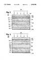
- FIG. 1is a graph of the current-voltage characteristic of a prior art photovoltaic device and the current-voltage characteristic of a preferred embodiment of the claimed invention
- FIG. 2is a cross-sectional view of an amorphous silicon multijunction photovoltaic device constructed in accordance with a first embodiment of the present invention.
- FIG. 3is a cross-sectional view of an amorphous silicon multijunction photovoltaic device constructed in accordance with a second embodiment of the present invention.
- Device 200includes a substrate 202 having an incident surface 204 for receiving solar radiation 206.
- Substrate 202preferably comprises glass or another suitable material which is transparent to solar radiation.
- a front conductive contact layer 208is formed on substrate 202.
- Front conductive layer 208is preferably an optically transparent conductor such as a metal oxide, e.g., tin oxide.
- Photovoltaic cell 210is comprised of a p-type hydrogenated amorphous silicon carbide (a-SiC:H) layer 220 deposited on front conductive layer 208, an intrinsic hydrogenated amorphous silicon layer 222 formed on p-type layer 220, and an n-type a-SiC:H layer 224 formed on intrinsic layer 222.
- a-SiC:Hhydrogenated amorphous silicon carbide
- Photovoltaic cell 212has substantially the same basic structure as that of photovoltaic cell 210, in that it is comprised of a p-type a-SiC:H layer 230, an intrinsic hydrogenated amorphous silicon layer 232, and an n-type a-SiC:H layer 234.
- the p- and n-type layers, of cells 210 and 212include carbon concentrations of approximately 20% and 15%, respectively, at least adjacent to the intrinsic layer in each cell.
- a grading of the carbon concentration in each of n-type layer 224 and p-type layer 230is described more fully below with respect to a method for constructing device 200. It is noted that while both the p- and n- type layers of cells 210 and 212 include carbon, a multijunction device can be constructed in accordance with the invention without including a bandgap widening element in all doped layers.
- intrinsic layers 222 and 232are substantially free of such bandgap widening elements.
- narrow portions of the intrinsic layer, respectively in contact with the p- and n- type layers containing carbon,can include a small, graded concentration of carbon.
- intrinsic layers 222 and 232can include light p-type doping, e.g., a concentration of boron of less than 10 17 cm -3 , which is known to improve carrier generation capability of the intrinsic layer.
- Exemplary thicknesses and doping concentrations of the layers constituting each cell 210 and 212are disclosed in the above-incorporated U.S. Pat. No. 4,272,641.
- Device 200also includes a back contact layer 236 formed on n-type layer 234 and preferably provided as a metal such as aluminum.
- An interface layer 240 of relatively low bandgap, high conductivity semiconductor materialis interposed between the n-type a-SiC:H layer 224 of photovoltaic cell 210 and the p-type a-SiC:H layer 230 of photovoltaic cell 212.
- layer 240has a lower bandgap than either of adjacent layers 224 or 230 and can be provided as a p- or n-type semiconductor material that forms an ohmic contact with the adjacent one of layers 224 and 230 of the same conductivity type and that forms a tunnel junction with the one of layers 224 and 230 of the opposite conductivity type.
- layer 240Since layer 240 has a lower bandgap, it also has a higher electrical conductivity than either of adjacent layers 224 and 230. In general, while layers 224 and 230 can each have a bandgap on the order of 1.9 eV, the bandgap of layer 240 is preferably on the order of less than 1.7 eV.
- interface layer 240is provided as a p + -type hydrogenated amorphous silicon layer substantially free of carbon, nitrogen, fluorine or similar bandgap widening elements.
- Layer 240 so providedpreferably has a thickness in the range of 10 ⁇ to 200 ⁇ and preferably approximately 20 ⁇ , and is preferably doped with an acceptor dopant, such as boron, to a concentration of approximately 1%.
- an acceptor dopantsuch as boron
- interface layer 240is provided as a microcrystalline layer of n + -type hydrogenated silicon that is substantially free of carbon, nitrogen, fluorine or other bandgap widening elements.
- microcrystallinedescribes a material whose crystalline order is in the range of substantially 25 ⁇ to 500 ⁇ .
- the presence of microcrystallinitycan be determined by one or more of electron diffraction, x-ray diffraction, or Raman scattering spectroscopy. Since doped microcrystalline silicon is an indirect bandgap material having a relatively low bandgap, e.g., approximately 1.1 ev, it provides the dual advantages of high conductivity and high optical transmissivity.
- Layer 240 provided as a microcrystalline n + -type layerpreferably has a thickness in the range of 15 ⁇ to 50 ⁇ and preferably approximately 50 ⁇ , and is preferably doped with a donor dopant, such as phosphorus, to a concentration of approximately 1%.
- layer 240 provided as an n + -type microcrystalline layerforms a highly conductive, ohmic contact with n-type layer 224 of cell 210 and a tunnel junction with p-type layer 230 of cell 212.
- Layer 240 provided as a microcrystalline layerhas a relatively low optical bandgap but retains a high optical transmissivity because it is an indirect optical bandgap material.
- the carbon concentration of layer 224be graded from a maximum value at the interface with adjacent intrinsic layer 222 to a minimum value, preferably a zero concentration, at the interface with layer 240. Such grading can be achieved by either a stepped or continuous grading of the carbon concentration.
- carbonis included in n-type layer 224, across all or part of the thickness of layer, in order to increase the optical bandgap of that layer.
- the presence of carbondecreases the conductivity of each of layers 224 and 230.
- the carbon concentration of layer 224is preferably graded so that the bandgap and hence the conductivity of layer 224 has a maximum value at the interface with layer 240 and can better form a conductive contact therewith.
- the enhanced conductive contact between a graded n-type layer 224 and layer 240 provided as a p + -type layerresults in improved performance of the tunnel junction formed therebetween.
- p-type layer 230 of cell 212can also be provided with a carbon concentration that is graded, by steps or continuously, from a maximum value at its interface with intrinsic layer 232 to a minimum value, e.g., zero concentration, at the interface with layer 240.
- a minimum valuee.g., zero concentration
- Such grading of layer 230improves its conductive contact with layer 240.
- the present inventorshave observed that the open circuit voltage of a cell decreases when the p-layer is graded, while the cell open circuit voltage is not particularly sensitive to grading of the n-layer.
- n-type layer 224has a graded carbon concentration.
- layer 240consists of a first sublayer of n + -type a-Si:H, adjacent to layer 224, and a second sublayer of microcrystalline n + -type layer. The second sublayer is disposed between the first sublayer and layer 230 of cell 212 and is otherwise as described above with respect to the second variation of the first embodiment.
- the a-Si:H n + -type sublayeris substantially free of bandgap widening elements, has a thickness in the range of 10 ⁇ to 100 ⁇ and preferably 15 ⁇ , and is preferably doped with phosphorus to a concentration of approximately 1% cm -3 .
- the tunnel junction formed between interface layer 240 and one of layers 224 and 230functions with a substantially resistive characteristic so that the IV characteristic of device 200 is represented by curve 150 in FIG. 1.
- curve 150does not include the inflection found in curve 100.
- device 200 constructed to include a tunnel junction in accordance with the first embodiment of the inventionenjoys an improved fill factor and power generation capability.
- interface layer 240is comprised of a silicon compound having substantially the same index of refraction as adjacent layers 224 and 230. As a result, device 200 does not experience undesirable reflectivity at the interfaces with layer 240.
- the method for constructing device 200 in accordance with the first variation of the first embodimentis described first. All semiconductor layers of device 200 are formed by a glow discharge deposition process.
- the described methodincludes a method for providing each of n-type layer 224 and p-type layer 230 with a graded carbon concentration.
- layer 224is formed by depositing successively narrower optical bandgap a-SiC alloys by gradually removing carbon during the deposition process.
- deposition of the wide bandgap portion of n-layer 224, adjacent intrinsic layer 222begins with a mixture of 125 sccm PH 3 -SiH 4 +25 sccm SiH 4 +25 sccm methane.
- Layer 224is deposited by either dc or rf glow discharge using a power of 0.4 watts/in 2 yielding a deposition rate of about 4 ⁇ /second.
- Two or more layers, or a continuous grading out of carbon,are deposited in succession with the carbon being gradually removed, producing a total thickness of layer 224 of nominally 100 ⁇ .
- the stepped grading of carboncan be accomplished over three layers.
- the final gas mixtureis 125 sccm PH3-SiH 4 +75 sccm SiH 4 .
- Layer 240 provided as a p + -type layeris then deposited by glow discharge to a 20 ⁇ thickness from a mixture of 100 sccm 0.5% diborane-SiH 4 +100 sccm SiH 4 .
- p-type a-SiC:H layer 230is deposited by glow discharge to a thickness of approximately 100 ⁇ .
- the layeris initially deposited from a mixture of 30 sccm 0.5% diborane-SiH 4 +90 sccm SiH 4 .
- Two or more layers, or a continuous grading of carbon,are deposited in succession so that the final mixture from which the layer is deposited includes 80 sccm methane. If the bandgap of layer 230 is not graded, the mixture continuously includes 80 sccm methane. Suitable flushes are provided between depositions to avoid cross contamination. However, the entire fabrication process is carried out with a single glow discharge deposition system.
- n-type a-SiC:H layer 224is deposited by dc or rf discharge to a thickness of about 100 ⁇ using 125 sccm 4.5% PH 3 -SiH 4 mixture+25 sccm CH 4 +75 sccm SiH 4 using approximately 0.4 watts/in 2 at about 0.5 torr.
- Layer 240 as a microcrystalline n-type layeris deposited next.
- the formation of a microcrystalline doped layerhas in the past been difficult to achieve for the extremely thin (10-100 ⁇ ) layers required to maintain high optical transmission.
- This limitationhas been overcome by using a high intensity hydrogen glow discharge process to crystallize an amorphous layer which then acts as the "seed" nuclei for the further growth of the crystalline phase.
- a 20 ⁇ thick non-carbon containing n-type layer of hydrogenated p-type siliconis deposited using gas flow rates of 125 sccm of 4.5% PH 3 -SiH 4 +100 sccm SiH 4 .
- a 4 second glow discharge deposition at 0.5 torr and 0.4 watts/in 2is used to form the layer.
- the amorphous deposited layeris recrystallized by using a hydrogen plasma created at 1.5 torr (320 sccm flow rate) for 5 minutes at an rf or dc power level of approximately 2 watts/in 2 .
- the microcrystalline n-layeris deposited at 1.5 torr using a 2 watt/in 2 glow discharge with a flow rate of 5 sccm of 4.5% PH 3 in SiH 4 diluted in a 320 sccm flow of pure hydrogen.
- the depositionis conducted for 50 seconds yielding an approximate thickness of 50 ⁇ .
- p-type a-SiC layer 230 of cell 212is deposited for 17 seconds at 0.5 torr from a gas mixture of 25 sccm 0.5% B 2 H 6 in SiH 4 +80 sccm methane+100 sccm SiH 4 at an rf or dc power level of approximately 0.4 watt/in 2 .
- the carbon concentration of layer 224is graded out in the manner described above.
- the n + -type a-Si:H sublayeris deposited by a glow discharge to a thickness of approximately 100 ⁇ from a mixture of 125 sccm PH 3 -SiH 4 +75 sccm SiH 4 .
- the n + -type microcrystalline sublayer and p + -type layer 230are deposited as described above for the second variation of the first embodiment.
- FIG. 3illustrates a multijunction photovoltaic device 300 constructed in accordance with a second embodiment of the invention.
- Device 300includes substrate 202, front conductive layer 208 and photovoltaic cells 210 and 212 as described above for device 200.
- Device 300also includes an interface layer 302 comprised of layers 304 and 306 sandwiched between n-type layer 224 of device 210 and p-type layer 230 of device 212 such that layer 304 is in contact with layer 224 and layer 306 is in contact with layer 230.
- layers 304 and 306are respectively provided as n-type and p-type hydrogenated silicon layers each having a relatively low bandgap.
- each of layers 304 and 306has a lower bandgap, and therefore a higher conductivity, than layers 224 and 230.
- n-layer 304forms a highly conductive, ohmic contact with n-type layer 224
- p-type layer 306forms a highly conductive, ohmic contact with p-type layer 230
- a tunnel junctionis formed between layers 304 and 306.
- the bandgap of each of layers 304 and 306is on the order described above for layer 240 of the first embodiment.
- layer 304is provided as a microcrystalline layer of n + -type hydrogenated silicon that is substantially free of carbon, nitrogen, fluorine or other bandgap widening elements.
- Layer 304has a thickness in the range of 10 ⁇ to 100 ⁇ and preferably approximately 20 ⁇ , and a dopant concentration of approximately 1%.
- Layer 306is provided as a layer of p + -type hydrogenated amorphous silicon that is substantially free of the above noted bandgap widening elements.
- Layer 306has a thickness in the range of 5 ⁇ to 100 ⁇ and preferably approximately 15 ⁇ , and a dopant concentration of approximately 1%.
- layer 304is provided as a layer of n + -type hydrogenated amorphous silicon that is substantially free of the above-noted bandgap widening elements.
- Layer 304 so providedhas a thickness in the range of 10 ⁇ to 100 ⁇ and preferably approximately 15 ⁇ , and a dopant concentration of approximately 1%.
- Layer 306 of this variationis the same as described above for the first variation.
- layer 304is provided as a microcrystalline layer of n + -type hydrogenated silicon as described above for the first variation.
- layer 306is provided as a microcrystalline layer of p + -type hydrogenated silicon that is substantially free of the above-noted bandgap widening elements.
- layer 306has a thickness in the range of 10 ⁇ to 100 ⁇ and preferably approximately 15 ⁇ , and a dopant concentration of approximately 1%.
- layer 306is provided as described for the third variation and layer 304 is provided as described for the second variation.
- n-type layer 224 and p-type layer 230each provided with a uniform carbon concentration throughout.
- the carbon concentration of layer 224be graded as described above with respect to the first embodiment.
- the carbon concentration of p-layer 230can also be graded as previously described.
- the tunnel-junction formed between layers 304 and 306functions with a substantially resistive characteristic so that the IV characteristic of device 300, like device 200, is also represented by curve 150 in FIG. 1.
- device 300 constructed in accordance with the second embodiment of the inventionenjoys an improved fill factor and power generation capability.
- layers 304 and 306are each comprised of a silicon compound having substantially the same index of refraction as layers 224 and 230. As a result, device 300 does not experience undesirable reflectivity at the interfaces with layer 302.
- p + -type microcrystalline layer 306 of the third and fourth variationscan be formed in a manner analogous to that described above for forming the n + -type microcrystalline layer.
- layer 306can be deposited from a mixture of 0.5% diborane in silane diluted with 320 sccm hydrogen, by glow discharge with a power of 2 watts/in 2 .
- devices 200 and 300 constructed in accordance with embodiments of the inventionhave been described as including carbon in their respective n-type and p-type layers as a bandgap widening element, the invention is not so limited.
- the inventioncan be practiced with equal effectiveness using a bandgap widening element other than carbon, e.g., fluorine, nitrogen, or oxygen.
- devices 200 and 300each include only two photovoltaic cells
- the inventioncan be practiced with multijunction photovoltaic devices that include more than two cells.
- an interface layer constructed in accordance with the inventionwould be interposed between each pair of adjacent photovoltaic cells in the multijunction device.
- the following exampleillustrates the advantages realized from constructing a multijunction photovoltaic device to include an interface layer that forms a tunnel junction with an adjacent cell layer.
- two multijunction devicesdesignated device #1 and device #2, were constructed. Both devices #1 and #2 included two PIN type photovoltaic cells having characteristics as described above for the illustrated embodiments.
- Device #1did not include an interface layer.
- Device #2included an interface layer such as described above for the first variation of the first embodiment of the invention.
- the interface layerwas comprised of a boron doped p + -type hydrogenated amorphous silicon layer substantially free of carbon, nitrogen, fluorine or other bandgap widening elements.
- the interface layerhad a thickness of approximately 20 ⁇ and a boron concentration of approximately 0.3%.
- devices #1 and #2were identical except for the inclusion of the interface layer in device #2.
- Table 1lists performance characteristics of devices #1 and #2 measured under identical irradiation conditions.
- Voc and Jscare respectively the open circuit voltage and short circuit current density of the device.
- the inclusion of the interface layer in device #2results in an 8.6% increase in fill factor which is reflected by the corresponding increase in device efficiency.
- the inclusion of the interface layer in device #2results in a substantial reduction in the series resistance of the multijunction device.
Landscapes
- Photovoltaic Devices (AREA)
Abstract
Description
TABLE 1 ______________________________________ Device #1 Device #2 ______________________________________ Voc 2.141 volts 2.225 volts Jsc -6.4 ma/cm.sup.2 -6.5 ma/cm.sup.2 Fill Factor 58.1% 63.1% Efficiency 7.9% 9.2% Rs 129.16 ohm-cm.sup.2 54.89 ohm-cm.sup.2 ______________________________________
Claims (23)
Priority Applications (5)
| Application Number | Priority Date | Filing Date | Title |
|---|---|---|---|
| US07/730,177US5246506A (en) | 1991-07-16 | 1991-07-16 | Multijunction photovoltaic device and fabrication method |
| EP92306319AEP0523919B1 (en) | 1991-07-16 | 1992-07-09 | Multijunction photovoltaic device and fabrication method |
| DE69217287TDE69217287T2 (en) | 1991-07-16 | 1992-07-09 | Multi-junction photovoltaic device and manufacturing method |
| JP23127092AJP3218320B2 (en) | 1991-07-16 | 1992-07-15 | Multi-junction photoelectric device and method of manufacturing the same |
| US08/077,769US5403404A (en) | 1991-07-16 | 1993-06-18 | Multijunction photovoltaic device and method of manufacture |
Applications Claiming Priority (1)
| Application Number | Priority Date | Filing Date | Title |
|---|---|---|---|
| US07/730,177US5246506A (en) | 1991-07-16 | 1991-07-16 | Multijunction photovoltaic device and fabrication method |
Related Child Applications (1)
| Application Number | Title | Priority Date | Filing Date |
|---|---|---|---|
| US08/077,769Continuation-In-PartUS5403404A (en) | 1991-07-16 | 1993-06-18 | Multijunction photovoltaic device and method of manufacture |
Publications (1)
| Publication Number | Publication Date |
|---|---|
| US5246506Atrue US5246506A (en) | 1993-09-21 |
Family
ID=24934268
Family Applications (2)
| Application Number | Title | Priority Date | Filing Date |
|---|---|---|---|
| US07/730,177Expired - LifetimeUS5246506A (en) | 1991-07-16 | 1991-07-16 | Multijunction photovoltaic device and fabrication method |
| US08/077,769Expired - LifetimeUS5403404A (en) | 1991-07-16 | 1993-06-18 | Multijunction photovoltaic device and method of manufacture |
Family Applications After (1)
| Application Number | Title | Priority Date | Filing Date |
|---|---|---|---|
| US08/077,769Expired - LifetimeUS5403404A (en) | 1991-07-16 | 1993-06-18 | Multijunction photovoltaic device and method of manufacture |
Country Status (4)
| Country | Link |
|---|---|
| US (2) | US5246506A (en) |
| EP (1) | EP0523919B1 (en) |
| JP (1) | JP3218320B2 (en) |
| DE (1) | DE69217287T2 (en) |
Cited By (32)
| Publication number | Priority date | Publication date | Assignee | Title |
|---|---|---|---|---|
| US5403404A (en)* | 1991-07-16 | 1995-04-04 | Amoco Corporation | Multijunction photovoltaic device and method of manufacture |
| US5730808A (en)* | 1996-06-27 | 1998-03-24 | Amoco/Enron Solar | Producing solar cells by surface preparation for accelerated nucleation of microcrystalline silicon on heterogeneous substrates |
| US6077722A (en)* | 1998-07-14 | 2000-06-20 | Bp Solarex | Producing thin film photovoltaic modules with high integrity interconnects and dual layer contacts |
| US6111189A (en)* | 1998-07-28 | 2000-08-29 | Bp Solarex | Photovoltaic module framing system with integral electrical raceways |
| US6121541A (en)* | 1997-07-28 | 2000-09-19 | Bp Solarex | Monolithic multi-junction solar cells with amorphous silicon and CIS and their alloys |
| US6294725B1 (en) | 2000-03-31 | 2001-09-25 | Trw Inc. | Wireless solar cell array electrical interconnection scheme |
| US20030153198A1 (en)* | 2001-07-20 | 2003-08-14 | Conti Richard A. | Carbon-graded layer for improved adhesion of low-k dielectrics to silicon substrates |
| WO2003085746A1 (en)* | 2002-04-09 | 2003-10-16 | Kaneka Corporation | Method for fabricating tandem thin film photoelectric converter |
| US20050229965A1 (en)* | 2004-03-24 | 2005-10-20 | Sharp Kabushiki Kaisha | Photoelectric conversion device and manufacturing method thereof |
| US20080135083A1 (en)* | 2006-12-08 | 2008-06-12 | Higher Way Electronic Co., Ltd. | Cascade solar cell with amorphous silicon-based solar cell |
| EP2056362A2 (en) | 2007-10-29 | 2009-05-06 | Waffenschmidt, Lynn | Multi-junction multi-spectral solar converter |
| US20090272430A1 (en)* | 2008-04-30 | 2009-11-05 | Emcore Solar Power, Inc. | Refractive Index Matching in Inverted Metamorphic Multijunction Solar Cells |
| US20100012175A1 (en)* | 2008-07-16 | 2010-01-21 | Emcore Solar Power, Inc. | Ohmic n-contact formed at low temperature in inverted metamorphic multijunction solar cells |
| US20100029067A1 (en)* | 2008-08-04 | 2010-02-04 | Aarohi Vijh | Roll-to-roll continuous thin film pv manufacturing process and equipment with real time online iv measurement |
| US20100024729A1 (en)* | 2008-08-04 | 2010-02-04 | Xinmin Cao | Methods and apparatuses for uniform plasma generation and uniform thin film deposition |
| US7741144B2 (en)* | 2007-11-02 | 2010-06-22 | Applied Materials, Inc. | Plasma treatment between deposition processes |
| US20110088760A1 (en)* | 2009-10-20 | 2011-04-21 | Applied Materials, Inc. | Methods of forming an amorphous silicon layer for thin film solar cell application |
| KR101039719B1 (en)* | 2010-03-26 | 2011-06-09 | 한국철강 주식회사 | Photovoltaic device comprising a flexible substrate or an flexible substrate and a method of manufacturing the same |
| KR101043219B1 (en)* | 2010-04-05 | 2011-06-22 | 한국철강 주식회사 | Method of manufacturing a photovoltaic device comprising a flexible substrate or an flexible substrate |
| US20110226318A1 (en)* | 2010-03-17 | 2011-09-22 | Seung-Yeop Myong | Photovoltaic device including flexible or inflexibel substrate and method for manufacturing the same |
| US8203071B2 (en) | 2007-01-18 | 2012-06-19 | Applied Materials, Inc. | Multi-junction solar cells and methods and apparatuses for forming the same |
| US20130000689A1 (en)* | 2011-07-01 | 2013-01-03 | Miasolé | Photovoltaic module support assembly with standoff clamps |
| US20130069193A1 (en)* | 2010-05-26 | 2013-03-21 | Katsushi Kishimoto | Intermediate layer for stacked type photoelectric conversion device, stacked type photoelectric conversion device and method for manufacturing stacked type photoelectric conversion device |
| CN103022269A (en)* | 2011-09-22 | 2013-04-03 | 吉富新能源科技(上海)有限公司 | P type amorphous semiconductor manufactured by utilizing boron doping to improve tunneling effect film |
| CN103022209A (en)* | 2011-09-22 | 2013-04-03 | 吉富新能源科技(上海)有限公司 | Manufacturing of efficient dual-junction silicon thin-film solar cell employing novel interlayer metallic oxide |
| US20130081685A1 (en)* | 2010-05-27 | 2013-04-04 | Kazuhito Nishimura | Photoelectric conversion device |
| CN103077981A (en)* | 2011-10-26 | 2013-05-01 | 上海空间电源研究所 | Flexible substrate silicon-based multi-junction laminated thin-film solar battery and manufacturing method thereof |
| JP2014135343A (en)* | 2013-01-09 | 2014-07-24 | Sharp Corp | Photoelectric conversion element, and method of manufacturing the same |
| US20150083203A1 (en)* | 2012-04-03 | 2015-03-26 | Lg Electronics Inc. | Thin film solar cell |
| US9287438B1 (en)* | 2008-07-16 | 2016-03-15 | Solaero Technologies Corp. | Method for forming ohmic N-contacts at low temperature in inverted metamorphic multijunction solar cells with contaminant isolation |
| US10403779B2 (en)* | 2012-05-10 | 2019-09-03 | International Business Machines Corporation | Cost-efficient high power PECVD deposition apparatus for solar cells |
| WO2024260463A1 (en)* | 2023-06-21 | 2024-12-26 | 华能新能源股份有限公司 | Photovoltaic cell module and manufacturing method therefor, and photovoltaic device |
Families Citing this family (35)
| Publication number | Priority date | Publication date | Assignee | Title |
|---|---|---|---|---|
| FR2743193B1 (en)* | 1996-01-02 | 1998-04-30 | Univ Neuchatel | METHOD AND DEVICE FOR DEPOSITING AT LEAST ONE INTRINSIC MICRO-CRYSTAL OR NANOCRYSTALLINE SILICON LAYER, AND THIN-LAYER PHOTOVOLTAIC CELL AND TRANSISTOR OBTAINED BY CARRYING OUT THIS PROCESS |
| US5936193A (en)* | 1997-05-09 | 1999-08-10 | Parise; Ronald J. | Nighttime solar cell |
| US20060021648A1 (en)* | 1997-05-09 | 2006-02-02 | Parise Ronald J | Device and method to transmit waste heat or thermal pollution into deep space |
| US6166318A (en)* | 1998-03-03 | 2000-12-26 | Interface Studies, Inc. | Single absorber layer radiated energy conversion device |
| TW565812B (en)* | 2000-07-21 | 2003-12-11 | Ebauchesfabrik Eta Ag | Display assembly including an electro-optical cell and a photovoltaic cell |
| US6566159B2 (en)* | 2000-10-04 | 2003-05-20 | Kaneka Corporation | Method of manufacturing tandem thin-film solar cell |
| KR101008274B1 (en)* | 2003-07-24 | 2011-01-14 | 가부시키가이샤 가네카 | Stacked Photoelectric Converters |
| JP4063735B2 (en)* | 2003-07-24 | 2008-03-19 | 株式会社カネカ | Thin film photoelectric conversion module including stacked photoelectric conversion device |
| JP4945088B2 (en)* | 2005-04-28 | 2012-06-06 | 三洋電機株式会社 | Stacked photovoltaic device |
| US20090165839A1 (en)* | 2005-12-02 | 2009-07-02 | Miroslav Zeman | Photovoltaic Cell |
| US11211510B2 (en)* | 2005-12-13 | 2021-12-28 | The Boeing Company | Multijunction solar cell with bonded transparent conductive interlayer |
| US20070240759A1 (en)* | 2006-04-13 | 2007-10-18 | Applied Materials, Inc. | Stacked thin film photovoltaic module and method for making same using IC processing |
| US20080173350A1 (en)* | 2007-01-18 | 2008-07-24 | Applied Materials, Inc. | Multi-junction solar cells and methods and apparatuses for forming the same |
| US20080223440A1 (en)* | 2007-01-18 | 2008-09-18 | Shuran Sheng | Multi-junction solar cells and methods and apparatuses for forming the same |
| US7582515B2 (en)* | 2007-01-18 | 2009-09-01 | Applied Materials, Inc. | Multi-junction solar cells and methods and apparatuses for forming the same |
| JP4484886B2 (en)* | 2007-01-23 | 2010-06-16 | シャープ株式会社 | Manufacturing method of stacked photoelectric conversion device |
| DE102007033444A1 (en)* | 2007-07-18 | 2009-01-29 | Schott Solar Gmbh | Silicon multiple solar cell and process for its production |
| US20090104733A1 (en)* | 2007-10-22 | 2009-04-23 | Yong Kee Chae | Microcrystalline silicon deposition for thin film solar applications |
| US20090130827A1 (en)* | 2007-11-02 | 2009-05-21 | Soo Young Choi | Intrinsic amorphous silicon layer |
| US20100300505A1 (en)* | 2009-05-26 | 2010-12-02 | Chen Yung T | Multiple junction photovolatic devices and process for making the same |
| US9178091B2 (en) | 2009-07-20 | 2015-11-03 | Soitec | Methods of fabricating semiconductor structures and devices using quantum dot structures and related structures |
| CN102117860B (en)* | 2010-01-06 | 2013-07-31 | 京东方科技集团股份有限公司 | Three-laminated-layer thin film solar cell and preparation method thereof |
| TWI470818B (en)* | 2010-03-24 | 2015-01-21 | Hitachi Ltd | Solar battery |
| JP2011216586A (en)* | 2010-03-31 | 2011-10-27 | Sharp Corp | Laminated photoelectric conversion device and method of manufacturing the same |
| WO2012018649A2 (en)* | 2010-08-06 | 2012-02-09 | Spectrawatt, Inc. | Cooperative photovoltaic networks and photovoltaic cell adaptations for use therein |
| US8859321B2 (en)* | 2011-01-31 | 2014-10-14 | International Business Machines Corporation | Mixed temperature deposition of thin film silicon tandem cells |
| JP2013038336A (en)* | 2011-08-10 | 2013-02-21 | Toshiba Corp | Semiconductor device |
| US9117965B2 (en)* | 2011-10-28 | 2015-08-25 | Dow Global Technologies Llc | Method of manufacture of chalcogenide-based photovoltaic cells |
| KR20130130915A (en)* | 2012-05-23 | 2013-12-03 | 경희대학교 산학협력단 | 2d transition metal dichalcogenides device with multi-layers and semiconductor device |
| US9508881B2 (en) | 2012-10-11 | 2016-11-29 | Sandia Corporation | Transparent contacts for stacked compound photovoltaic cells |
| TWI469380B (en)* | 2013-11-08 | 2015-01-11 | Ind Tech Res Inst | Heterojunction solar cell structure |
| CN105470339A (en)* | 2014-08-08 | 2016-04-06 | 上海建冶环保科技股份有限公司 | Nanosilicon thin-film multi-junction solar cell |
| TWI596791B (en)* | 2015-12-07 | 2017-08-21 | 財團法人工業技術研究院 | Solar battery module |
| US20180331157A1 (en) | 2017-05-15 | 2018-11-15 | International Business Machines Corporation | Multi-junction photovoltaic cells |
| EP3442036B1 (en)* | 2017-08-09 | 2020-06-24 | AE 111 Autarke Energie GmbH | Optoelectronic semiconductor element |
Citations (13)
| Publication number | Priority date | Publication date | Assignee | Title |
|---|---|---|---|---|
| US4167015A (en)* | 1978-04-24 | 1979-09-04 | Rca Corporation | Cermet layer for amorphous silicon solar cells |
| US4166918A (en)* | 1978-07-19 | 1979-09-04 | Rca Corporation | Method of removing the effects of electrical shorts and shunts created during the fabrication process of a solar cell |
| US4255211A (en)* | 1979-12-31 | 1981-03-10 | Chevron Research Company | Multilayer photovoltaic solar cell with semiconductor layer at shorting junction interface |
| US4272641A (en)* | 1979-04-19 | 1981-06-09 | Rca Corporation | Tandem junction amorphous silicon solar cells |
| US4292092A (en)* | 1980-06-02 | 1981-09-29 | Rca Corporation | Laser processing technique for fabricating series-connected and tandem junction series-connected solar cells into a solar battery |
| US4297720A (en)* | 1978-07-21 | 1981-10-27 | Sumitomo Electric Industries, Ltd. | Multi-photodiodes |
| US4316049A (en)* | 1979-08-28 | 1982-02-16 | Rca Corporation | High voltage series connected tandem junction solar battery |
| US4377723A (en)* | 1980-05-02 | 1983-03-22 | The University Of Delaware | High efficiency thin-film multiple-gap photovoltaic device |
| US4471155A (en)* | 1983-04-15 | 1984-09-11 | Energy Conversion Devices, Inc. | Narrow band gap photovoltaic devices with enhanced open circuit voltage |
| JPS6011478A (en)* | 1983-06-30 | 1985-01-21 | Showa Denko Kk | Oxadiazolinon derivative and herbicide |
| JPS62296569A (en)* | 1986-06-17 | 1987-12-23 | Sumitomo Electric Ind Ltd | Tandem structure solar cell |
| US4776894A (en)* | 1986-08-18 | 1988-10-11 | Sanyo Electric Co., Ltd. | Photovoltaic device |
| US4926230A (en)* | 1986-04-04 | 1990-05-15 | Kanegafuchi Kagaku Kogyo Kabushiki Kaisha | Multiple junction solar power generation cells |
Family Cites Families (31)
| Publication number | Priority date | Publication date | Assignee | Title |
|---|---|---|---|---|
| US3801879A (en)* | 1971-03-09 | 1974-04-02 | Innotech Corp | Junction device employing a glassy amorphous material as an active layer |
| US3864718A (en)* | 1971-03-09 | 1975-02-04 | Innotech Corp | Multiple junction device employing a glassy amorphous material as an active layer |
| US3864717A (en)* | 1971-03-09 | 1975-02-04 | Innotech Corp | Photoresponsive junction device employing a glassy amorphous material as an active layer |
| US4174561A (en)* | 1976-02-09 | 1979-11-20 | Semicon, Inc. | Method of fabricating high intensity solar energy converter |
| US4492810A (en)* | 1978-03-08 | 1985-01-08 | Sovonics Solar Systems | Optimized doped and band gap adjusted photoresponsive amorphous alloys and devices |
| US4342044A (en)* | 1978-03-08 | 1982-07-27 | Energy Conversion Devices, Inc. | Method for optimizing photoresponsive amorphous alloys and devices |
| US4278474A (en)* | 1980-03-25 | 1981-07-14 | The United States Of America As Represented By The United States Department Of Energy | Device for conversion of electromagnetic radiation into electrical current |
| US4320247A (en)* | 1980-08-06 | 1982-03-16 | Massachusetts Institute Of Technology | Solar cell having multiple p-n junctions and process for producing same |
| US4891074A (en)* | 1980-11-13 | 1990-01-02 | Energy Conversion Devices, Inc. | Multiple cell photoresponsive amorphous alloys and devices |
| US4442185A (en)* | 1981-10-19 | 1984-04-10 | The United States Of America As Represented By The United States Department Of Energy | Photoelectrochemical cells for conversion of solar energy to electricity and methods of their manufacture |
| US4416959A (en)* | 1980-11-18 | 1983-11-22 | Terje Skotheim | Photoelectrochemical cells for conversion of solar energy to electricity |
| US4352868A (en)* | 1980-11-18 | 1982-10-05 | Terje Skotheim | Double photoelectrochemical cell for conversion of solar energy to electricity |
| US4341918A (en)* | 1980-12-24 | 1982-07-27 | The United States Of America As Represented By The Administrator Of The National Aeronautics And Space Administration | High voltage planar multijunction solar cell |
| US4387265A (en)* | 1981-07-17 | 1983-06-07 | University Of Delaware | Tandem junction amorphous semiconductor photovoltaic cell |
| JPS58139478A (en)* | 1982-02-15 | 1983-08-18 | Agency Of Ind Science & Technol | amorphous solar cell |
| US4485125A (en)* | 1982-03-19 | 1984-11-27 | Energy Conversion Devices, Inc. | Method for continuously producing tandem amorphous photovoltaic cells |
| US4479027A (en)* | 1982-09-24 | 1984-10-23 | Todorof William J | Multi-layer thin-film, flexible silicon alloy photovoltaic cell |
| US4633031A (en)* | 1982-09-24 | 1986-12-30 | Todorof William J | Multi-layer thin film, flexible silicon alloy photovoltaic cell |
| US4502225A (en)* | 1983-05-06 | 1985-03-05 | Rca Corporation | Mechanical scriber for semiconductor devices |
| JPS60111478A (en)* | 1983-11-22 | 1985-06-17 | Toshiba Corp | Photovoltaic device |
| EP0153043A3 (en)* | 1984-02-15 | 1986-09-24 | Energy Conversion Devices, Inc. | Ohmic contact layer |
| US4513168A (en)* | 1984-04-19 | 1985-04-23 | Varian Associates, Inc. | Three-terminal solar cell circuit |
| US4609771A (en)* | 1984-11-02 | 1986-09-02 | Sovonics Solar Systems | Tandem junction solar cell devices incorporating improved microcrystalline p-doped semiconductor alloy material |
| US4575576A (en)* | 1984-11-07 | 1986-03-11 | The United States Of America As Represented By The United States Department Of Energy | Three-junction solar cell |
| US4643817A (en)* | 1985-06-07 | 1987-02-17 | Electric Power Research Institute, Inc. | Photocell device for evolving hydrogen and oxygen from water |
| JPS6284571A (en)* | 1985-10-08 | 1987-04-18 | Sumitomo Electric Ind Ltd | Multilayer amorphous solar cell |
| US4642413A (en)* | 1985-10-11 | 1987-02-10 | Energy Conversion Devices, Inc. | Power generating optical filter |
| US4713493A (en)* | 1985-10-11 | 1987-12-15 | Energy Conversion Devices, Inc. | Power generating optical filter |
| US4713492A (en)* | 1985-10-21 | 1987-12-15 | Energy Conversion Devices, Inc. | Stowable large area solar power module |
| JPH0693519B2 (en)* | 1987-09-17 | 1994-11-16 | 株式会社富士電機総合研究所 | Amorphous photoelectric conversion device |
| US5246506A (en)* | 1991-07-16 | 1993-09-21 | Solarex Corporation | Multijunction photovoltaic device and fabrication method |
- 1991
- 1991-07-16USUS07/730,177patent/US5246506A/ennot_activeExpired - Lifetime
- 1992
- 1992-07-09DEDE69217287Tpatent/DE69217287T2/ennot_activeExpired - Fee Related
- 1992-07-09EPEP92306319Apatent/EP0523919B1/ennot_activeExpired - Lifetime
- 1992-07-15JPJP23127092Apatent/JP3218320B2/ennot_activeExpired - Fee Related
- 1993
- 1993-06-18USUS08/077,769patent/US5403404A/ennot_activeExpired - Lifetime
Patent Citations (13)
| Publication number | Priority date | Publication date | Assignee | Title |
|---|---|---|---|---|
| US4167015A (en)* | 1978-04-24 | 1979-09-04 | Rca Corporation | Cermet layer for amorphous silicon solar cells |
| US4166918A (en)* | 1978-07-19 | 1979-09-04 | Rca Corporation | Method of removing the effects of electrical shorts and shunts created during the fabrication process of a solar cell |
| US4297720A (en)* | 1978-07-21 | 1981-10-27 | Sumitomo Electric Industries, Ltd. | Multi-photodiodes |
| US4272641A (en)* | 1979-04-19 | 1981-06-09 | Rca Corporation | Tandem junction amorphous silicon solar cells |
| US4316049A (en)* | 1979-08-28 | 1982-02-16 | Rca Corporation | High voltage series connected tandem junction solar battery |
| US4255211A (en)* | 1979-12-31 | 1981-03-10 | Chevron Research Company | Multilayer photovoltaic solar cell with semiconductor layer at shorting junction interface |
| US4377723A (en)* | 1980-05-02 | 1983-03-22 | The University Of Delaware | High efficiency thin-film multiple-gap photovoltaic device |
| US4292092A (en)* | 1980-06-02 | 1981-09-29 | Rca Corporation | Laser processing technique for fabricating series-connected and tandem junction series-connected solar cells into a solar battery |
| US4471155A (en)* | 1983-04-15 | 1984-09-11 | Energy Conversion Devices, Inc. | Narrow band gap photovoltaic devices with enhanced open circuit voltage |
| JPS6011478A (en)* | 1983-06-30 | 1985-01-21 | Showa Denko Kk | Oxadiazolinon derivative and herbicide |
| US4926230A (en)* | 1986-04-04 | 1990-05-15 | Kanegafuchi Kagaku Kogyo Kabushiki Kaisha | Multiple junction solar power generation cells |
| JPS62296569A (en)* | 1986-06-17 | 1987-12-23 | Sumitomo Electric Ind Ltd | Tandem structure solar cell |
| US4776894A (en)* | 1986-08-18 | 1988-10-11 | Sanyo Electric Co., Ltd. | Photovoltaic device |
Non-Patent Citations (6)
| Title |
|---|
| "A Stable 10% Solar Cell With a-Si/a-Si Double-Junction Structure" by Ichikawa et al., Conf. Record of the IEEE Photovoltaic Specialists Conference, vol. 21, IEEE, pp. 1475-1480 (1990). |
| "Improving tunneling junction in amorphous silicon tandem solar cells" by Shen et al., Appl. Phys. Lett. 56(19), May 7, 1990, pp. 1871-1873. |
| "Stacked Solar Cells Of Amorphous Silicon" by Hanak, Journal of Non-Crystalline Solids 35 & 36 (1980), pp. 755-759. |
| A Stable 10% Solar Cell With a Si/a Si Double Junction Structure by Ichikawa et al., Conf. Record of the IEEE Photovoltaic Specialists Conference, vol. 21, IEEE, pp. 1475 1480 (1990).* |
| Improving tunneling junction in amorphous silicon tandem solar cells by Shen et al., Appl. Phys. Lett. 56(19), May 7, 1990, pp. 1871 1873.* |
| Stacked Solar Cells Of Amorphous Silicon by Hanak, Journal of Non Crystalline Solids 35 & 36 (1980), pp. 755 759.* |
Cited By (45)
| Publication number | Priority date | Publication date | Assignee | Title |
|---|---|---|---|---|
| US5403404A (en)* | 1991-07-16 | 1995-04-04 | Amoco Corporation | Multijunction photovoltaic device and method of manufacture |
| US5730808A (en)* | 1996-06-27 | 1998-03-24 | Amoco/Enron Solar | Producing solar cells by surface preparation for accelerated nucleation of microcrystalline silicon on heterogeneous substrates |
| US6121541A (en)* | 1997-07-28 | 2000-09-19 | Bp Solarex | Monolithic multi-junction solar cells with amorphous silicon and CIS and their alloys |
| US6077722A (en)* | 1998-07-14 | 2000-06-20 | Bp Solarex | Producing thin film photovoltaic modules with high integrity interconnects and dual layer contacts |
| US6111189A (en)* | 1998-07-28 | 2000-08-29 | Bp Solarex | Photovoltaic module framing system with integral electrical raceways |
| US6294725B1 (en) | 2000-03-31 | 2001-09-25 | Trw Inc. | Wireless solar cell array electrical interconnection scheme |
| US6740539B2 (en)* | 2001-07-20 | 2004-05-25 | International Business Machines Corporation | Carbon-graded layer for improved adhesion of low-k dielectrics to silicon substrates |
| US20030153198A1 (en)* | 2001-07-20 | 2003-08-14 | Conti Richard A. | Carbon-graded layer for improved adhesion of low-k dielectrics to silicon substrates |
| WO2003085746A1 (en)* | 2002-04-09 | 2003-10-16 | Kaneka Corporation | Method for fabricating tandem thin film photoelectric converter |
| US20050181534A1 (en)* | 2002-04-09 | 2005-08-18 | Masashi Yoshimi | Method for fabricating tandem thin film photoelectric converter |
| US7238545B2 (en) | 2002-04-09 | 2007-07-03 | Kaneka Corporation | Method for fabricating tandem thin film photoelectric converter |
| KR100847487B1 (en)* | 2002-04-09 | 2008-07-22 | 가부시키가이샤 가네카 | Manufacturing Method of Tandem Thin Film Photoelectric Conversion Device |
| US7915520B2 (en)* | 2004-03-24 | 2011-03-29 | Sharp Kabushiki Kaisha | Photoelectric conversion device and manufacturing method thereof |
| US20050229965A1 (en)* | 2004-03-24 | 2005-10-20 | Sharp Kabushiki Kaisha | Photoelectric conversion device and manufacturing method thereof |
| US20110146773A1 (en)* | 2004-03-24 | 2011-06-23 | Sharp Kabushiki Kaisha | Photoelectric conversion device and manufacturing method thereof |
| US20080135083A1 (en)* | 2006-12-08 | 2008-06-12 | Higher Way Electronic Co., Ltd. | Cascade solar cell with amorphous silicon-based solar cell |
| US8203071B2 (en) | 2007-01-18 | 2012-06-19 | Applied Materials, Inc. | Multi-junction solar cells and methods and apparatuses for forming the same |
| EP2056362A2 (en) | 2007-10-29 | 2009-05-06 | Waffenschmidt, Lynn | Multi-junction multi-spectral solar converter |
| US7741144B2 (en)* | 2007-11-02 | 2010-06-22 | Applied Materials, Inc. | Plasma treatment between deposition processes |
| US20090272430A1 (en)* | 2008-04-30 | 2009-11-05 | Emcore Solar Power, Inc. | Refractive Index Matching in Inverted Metamorphic Multijunction Solar Cells |
| US9287438B1 (en)* | 2008-07-16 | 2016-03-15 | Solaero Technologies Corp. | Method for forming ohmic N-contacts at low temperature in inverted metamorphic multijunction solar cells with contaminant isolation |
| US8753918B2 (en) | 2008-07-16 | 2014-06-17 | Emcore Solar Power, Inc. | Gallium arsenide solar cell with germanium/palladium contact |
| US8987042B2 (en) | 2008-07-16 | 2015-03-24 | Solaero Technologies Corp. | Ohmic N-contact formed at low temperature in inverted metamorphic multijunction solar cells |
| US20100012175A1 (en)* | 2008-07-16 | 2010-01-21 | Emcore Solar Power, Inc. | Ohmic n-contact formed at low temperature in inverted metamorphic multijunction solar cells |
| US9601652B2 (en) | 2008-07-16 | 2017-03-21 | Solaero Technologies Corp. | Ohmic N-contact formed at low temperature in inverted metamorphic multijunction solar cells |
| US8298339B2 (en)* | 2008-08-04 | 2012-10-30 | Xunlight Corporation | Roll-to-roll continuous thin film PV manufacturing process and equipment with real time online IV measurement |
| US20100024729A1 (en)* | 2008-08-04 | 2010-02-04 | Xinmin Cao | Methods and apparatuses for uniform plasma generation and uniform thin film deposition |
| US20100029067A1 (en)* | 2008-08-04 | 2010-02-04 | Aarohi Vijh | Roll-to-roll continuous thin film pv manufacturing process and equipment with real time online iv measurement |
| US20110088760A1 (en)* | 2009-10-20 | 2011-04-21 | Applied Materials, Inc. | Methods of forming an amorphous silicon layer for thin film solar cell application |
| US8502065B2 (en)* | 2010-03-17 | 2013-08-06 | Kisco | Photovoltaic device including flexible or inflexibel substrate and method for manufacturing the same |
| US20110226318A1 (en)* | 2010-03-17 | 2011-09-22 | Seung-Yeop Myong | Photovoltaic device including flexible or inflexibel substrate and method for manufacturing the same |
| KR101039719B1 (en)* | 2010-03-26 | 2011-06-09 | 한국철강 주식회사 | Photovoltaic device comprising a flexible substrate or an flexible substrate and a method of manufacturing the same |
| KR101043219B1 (en)* | 2010-04-05 | 2011-06-22 | 한국철강 주식회사 | Method of manufacturing a photovoltaic device comprising a flexible substrate or an flexible substrate |
| US20130069193A1 (en)* | 2010-05-26 | 2013-03-21 | Katsushi Kishimoto | Intermediate layer for stacked type photoelectric conversion device, stacked type photoelectric conversion device and method for manufacturing stacked type photoelectric conversion device |
| US20130081685A1 (en)* | 2010-05-27 | 2013-04-04 | Kazuhito Nishimura | Photoelectric conversion device |
| US20130000689A1 (en)* | 2011-07-01 | 2013-01-03 | Miasolé | Photovoltaic module support assembly with standoff clamps |
| CN103022269A (en)* | 2011-09-22 | 2013-04-03 | 吉富新能源科技(上海)有限公司 | P type amorphous semiconductor manufactured by utilizing boron doping to improve tunneling effect film |
| CN103022209A (en)* | 2011-09-22 | 2013-04-03 | 吉富新能源科技(上海)有限公司 | Manufacturing of efficient dual-junction silicon thin-film solar cell employing novel interlayer metallic oxide |
| CN103077981B (en)* | 2011-10-26 | 2015-12-09 | 上海空间电源研究所 | The silica-based many knot laminated film solar batteries of flexible substrate and manufacture method thereof |
| CN103077981A (en)* | 2011-10-26 | 2013-05-01 | 上海空间电源研究所 | Flexible substrate silicon-based multi-junction laminated thin-film solar battery and manufacturing method thereof |
| US20150083203A1 (en)* | 2012-04-03 | 2015-03-26 | Lg Electronics Inc. | Thin film solar cell |
| US10403779B2 (en)* | 2012-05-10 | 2019-09-03 | International Business Machines Corporation | Cost-efficient high power PECVD deposition apparatus for solar cells |
| US10672932B2 (en) | 2012-05-10 | 2020-06-02 | International Business Machines Corporation | Cost-efficient high power PECVD deposition for solar cells |
| JP2014135343A (en)* | 2013-01-09 | 2014-07-24 | Sharp Corp | Photoelectric conversion element, and method of manufacturing the same |
| WO2024260463A1 (en)* | 2023-06-21 | 2024-12-26 | 华能新能源股份有限公司 | Photovoltaic cell module and manufacturing method therefor, and photovoltaic device |
Also Published As
| Publication number | Publication date |
|---|---|
| EP0523919B1 (en) | 1997-02-05 |
| EP0523919A1 (en) | 1993-01-20 |
| JPH06151916A (en) | 1994-05-31 |
| DE69217287D1 (en) | 1997-03-20 |
| DE69217287T2 (en) | 1997-08-28 |
| JP3218320B2 (en) | 2001-10-15 |
| US5403404A (en) | 1995-04-04 |
Similar Documents
| Publication | Publication Date | Title |
|---|---|---|
| US5246506A (en) | Multijunction photovoltaic device and fabrication method | |
| US5256887A (en) | Photovoltaic device including a boron doping profile in an i-type layer | |
| US4496788A (en) | Photovoltaic device | |
| US5646050A (en) | Increasing stabilized performance of amorphous silicon based devices produced by highly hydrogen diluted lower temperature plasma deposition | |
| KR960015529B1 (en) | Thin film sola cell including a spatially modulated intrinsic layer | |
| US7879644B2 (en) | Hybrid window layer for photovoltaic cells | |
| US4718947A (en) | Superlattice doped layers for amorphous silicon photovoltaic cells | |
| US6368892B1 (en) | Monolithic multi-junction solar cells with amorphous silicon and CIS and their alloys | |
| EP0494088B1 (en) | Photovoltaic device | |
| US5913986A (en) | Photovoltaic element having a specific doped layer | |
| US7064263B2 (en) | Stacked photovoltaic device | |
| US5230746A (en) | Photovoltaic device having enhanced rear reflecting contact | |
| US8981200B2 (en) | Method for obtaining high performance thin film devices deposited on highly textured substrates | |
| EP0509215A1 (en) | Multi-layered photovoltaic element having at least three unit cells | |
| US4398054A (en) | Compensated amorphous silicon solar cell incorporating an insulating layer | |
| US4396793A (en) | Compensated amorphous silicon solar cell | |
| EP0437767B1 (en) | Enhancement of short-circuit current by use of wide bandgap n-layers in p-i-n amorphous silicon photovoltaic cells | |
| US5104455A (en) | Amorphous semiconductor solar cell | |
| JPS62115785A (en) | semiconductor equipment | |
| JPH0571195B2 (en) |
Legal Events
| Date | Code | Title | Description |
|---|---|---|---|
| AS | Assignment | Owner name:SOLAREX CORPORATION, MARYLAND Free format text:ASSIGNMENT OF ASSIGNORS INTEREST.;ASSIGNORS:ARYA, RAJEEWA R.;CATALANO, ANTHONY W.;REEL/FRAME:005830/0411 Effective date:19910815 | |
| STCF | Information on status: patent grant | Free format text:PATENTED CASE | |
| AS | Assignment | Owner name:AMOCO/ENRON SOLAR, MARYLAND Free format text:ASSIGNMENT OF ASSIGNORS INTEREST;ASSIGNORS:AMOCO CORPORATION;SOLAREX CORPORATION;REEL/FRAME:007289/0064 Effective date:19950101 | |
| FPAY | Fee payment | Year of fee payment:4 | |
| AS | Assignment | Owner name:ENERGY, DEPARTMENT OF, UNITED STATES, DISTRICT OF Free format text:CONFIRMATORY LICENSE;ASSIGNOR:SOLOREX CORPORATION;REEL/FRAME:008442/0408 Effective date:19950719 | |
| FPAY | Fee payment | Year of fee payment:8 | |
| FPAY | Fee payment | Year of fee payment:12 | |
| AS | Assignment | Owner name:BP SOLAREX, MARYLAND Free format text:CHANGE OF NAME;ASSIGNOR:AMOCO/ENRON SOLAR;REEL/FRAME:019419/0993 Effective date:19990714 | |
| AS | Assignment | Owner name:BP SOLAR INTERNATIONAL LLC, ILLINOIS Free format text:CHANGE OF NAME;ASSIGNOR:BP SOLAREX;REEL/FRAME:019440/0464 Effective date:20001221 | |
| AS | Assignment | Owner name:BP SOLAR INTERNATIONAL INC., ILLINOIS Free format text:MERGER;ASSIGNOR:BP SOLAR INTERNATIONAL LLC;REEL/FRAME:019477/0068 Effective date:20040401 |