US5245790A - Ultrasonic energy enhanced chemi-mechanical polishing of silicon wafers - Google Patents
Ultrasonic energy enhanced chemi-mechanical polishing of silicon wafersDownload PDFInfo
- Publication number
- US5245790A US5245790AUS07/837,444US83744492AUS5245790AUS 5245790 AUS5245790 AUS 5245790AUS 83744492 AUS83744492 AUS 83744492AUS 5245790 AUS5245790 AUS 5245790A
- Authority
- US
- United States
- Prior art keywords
- pad
- polishing
- wafer
- platen
- carrier
- Prior art date
- Legal status (The legal status is an assumption and is not a legal conclusion. Google has not performed a legal analysis and makes no representation as to the accuracy of the status listed.)
- Expired - Lifetime
Links
- 238000005498polishingMethods0.000titleclaimsabstractdescription63
- 235000012431wafersNutrition0.000titleclaimsabstractdescription46
- XUIMIQQOPSSXEZ-UHFFFAOYSA-NSiliconChemical compound[Si]XUIMIQQOPSSXEZ-UHFFFAOYSA-N0.000titledescription6
- 229910052710siliconInorganic materials0.000titledescription6
- 239000010703siliconSubstances0.000titledescription6
- 239000002002slurrySubstances0.000claimsabstractdescription31
- 230000033001locomotionEffects0.000claimsabstractdescription8
- 239000004065semiconductorSubstances0.000claimsabstractdescription8
- 238000000034methodMethods0.000abstractdescription27
- 238000007517polishing processMethods0.000abstractdescription9
- 239000000463materialSubstances0.000description10
- VYPSYNLAJGMNEJ-UHFFFAOYSA-NSilicium dioxideChemical compoundO=[Si]=OVYPSYNLAJGMNEJ-UHFFFAOYSA-N0.000description8
- 230000003750conditioning effectEffects0.000description7
- 230000001788irregularEffects0.000description7
- KWYUFKZDYYNOTN-UHFFFAOYSA-MPotassium hydroxideChemical group[OH-].[K+]KWYUFKZDYYNOTN-UHFFFAOYSA-M0.000description6
- 230000008569processEffects0.000description6
- 230000009471actionEffects0.000description4
- 230000035945sensitivityEffects0.000description4
- 239000000377silicon dioxideSubstances0.000description4
- 239000000126substanceSubstances0.000description4
- 239000004820Pressure-sensitive adhesiveSubstances0.000description3
- 238000000151depositionMethods0.000description3
- 230000008021depositionEffects0.000description3
- 238000004519manufacturing processMethods0.000description3
- 238000007521mechanical polishing techniqueMethods0.000description3
- 230000007246mechanismEffects0.000description3
- 230000010355oscillationEffects0.000description3
- 229920002635polyurethanePolymers0.000description3
- 239000004814polyurethaneSubstances0.000description3
- 238000012876topographyMethods0.000description3
- 230000008901benefitEffects0.000description2
- 230000015572biosynthetic processEffects0.000description2
- 230000008859changeEffects0.000description2
- 239000002131composite materialSubstances0.000description2
- 230000001143conditioned effectEffects0.000description2
- 230000000694effectsEffects0.000description2
- 238000005530etchingMethods0.000description2
- 238000005755formation reactionMethods0.000description2
- 229920005749polyurethane resinPolymers0.000description2
- 238000001039wet etchingMethods0.000description2
- 229910052684CeriumInorganic materials0.000description1
- 239000000853adhesiveSubstances0.000description1
- 230000001070adhesive effectEffects0.000description1
- 238000013019agitationMethods0.000description1
- 229910052792caesiumInorganic materials0.000description1
- TVFDJXOCXUVLDH-UHFFFAOYSA-Ncaesium atomChemical compound[Cs]TVFDJXOCXUVLDH-UHFFFAOYSA-N0.000description1
- GWXLDORMOJMVQZ-UHFFFAOYSA-NceriumChemical compound[Ce]GWXLDORMOJMVQZ-UHFFFAOYSA-N0.000description1
- 238000001311chemical methods and processMethods0.000description1
- 239000004020conductorSubstances0.000description1
- 238000001312dry etchingMethods0.000description1
- 239000013536elastomeric materialSubstances0.000description1
- 239000000835fiberSubstances0.000description1
- 230000005669field effectEffects0.000description1
- 239000000945fillerSubstances0.000description1
- 239000007789gasSubstances0.000description1
- 239000007792gaseous phaseSubstances0.000description1
- 239000011521glassSubstances0.000description1
- 238000000227grindingMethods0.000description1
- 230000003116impacting effectEffects0.000description1
- 238000011065in-situ storageMethods0.000description1
- 238000001465metallisationMethods0.000description1
- 238000012986modificationMethods0.000description1
- 230000004048modificationEffects0.000description1
- 239000002245particleSubstances0.000description1
- 238000001020plasma etchingMethods0.000description1
- 229920003023plasticPolymers0.000description1
- 239000004033plasticSubstances0.000description1
- 229920000728polyesterPolymers0.000description1
- 238000000992sputter etchingMethods0.000description1
- 230000002195synergetic effectEffects0.000description1
- WFKWXMTUELFFGS-UHFFFAOYSA-NtungstenChemical compound[W]WFKWXMTUELFFGS-UHFFFAOYSA-N0.000description1
- 229910052721tungstenInorganic materials0.000description1
- 239000010937tungstenSubstances0.000description1
Images


Classifications
- C—CHEMISTRY; METALLURGY
- C30—CRYSTAL GROWTH
- C30B—SINGLE-CRYSTAL GROWTH; UNIDIRECTIONAL SOLIDIFICATION OF EUTECTIC MATERIAL OR UNIDIRECTIONAL DEMIXING OF EUTECTOID MATERIAL; REFINING BY ZONE-MELTING OF MATERIAL; PRODUCTION OF A HOMOGENEOUS POLYCRYSTALLINE MATERIAL WITH DEFINED STRUCTURE; SINGLE CRYSTALS OR HOMOGENEOUS POLYCRYSTALLINE MATERIAL WITH DEFINED STRUCTURE; AFTER-TREATMENT OF SINGLE CRYSTALS OR A HOMOGENEOUS POLYCRYSTALLINE MATERIAL WITH DEFINED STRUCTURE; APPARATUS THEREFOR
- C30B33/00—After-treatment of single crystals or homogeneous polycrystalline material with defined structure
- B—PERFORMING OPERATIONS; TRANSPORTING
- B24—GRINDING; POLISHING
- B24B—MACHINES, DEVICES, OR PROCESSES FOR GRINDING OR POLISHING; DRESSING OR CONDITIONING OF ABRADING SURFACES; FEEDING OF GRINDING, POLISHING, OR LAPPING AGENTS
- B24B1/00—Processes of grinding or polishing; Use of auxiliary equipment in connection with such processes
- B24B1/04—Processes of grinding or polishing; Use of auxiliary equipment in connection with such processes subjecting the grinding or polishing tools, the abrading or polishing medium or work to vibration, e.g. grinding with ultrasonic frequency
- B—PERFORMING OPERATIONS; TRANSPORTING
- B24—GRINDING; POLISHING
- B24B—MACHINES, DEVICES, OR PROCESSES FOR GRINDING OR POLISHING; DRESSING OR CONDITIONING OF ABRADING SURFACES; FEEDING OF GRINDING, POLISHING, OR LAPPING AGENTS
- B24B37/00—Lapping machines or devices; Accessories
- B24B37/04—Lapping machines or devices; Accessories designed for working plane surfaces
- B—PERFORMING OPERATIONS; TRANSPORTING
- B24—GRINDING; POLISHING
- B24B—MACHINES, DEVICES, OR PROCESSES FOR GRINDING OR POLISHING; DRESSING OR CONDITIONING OF ABRADING SURFACES; FEEDING OF GRINDING, POLISHING, OR LAPPING AGENTS
- B24B53/00—Devices or means for dressing or conditioning abrasive surfaces
- B24B53/017—Devices or means for dressing, cleaning or otherwise conditioning lapping tools
- B—PERFORMING OPERATIONS; TRANSPORTING
- B24—GRINDING; POLISHING
- B24B—MACHINES, DEVICES, OR PROCESSES FOR GRINDING OR POLISHING; DRESSING OR CONDITIONING OF ABRADING SURFACES; FEEDING OF GRINDING, POLISHING, OR LAPPING AGENTS
- B24B7/00—Machines or devices designed for grinding plane surfaces on work, including polishing plane glass surfaces; Accessories therefor
- B24B7/20—Machines or devices designed for grinding plane surfaces on work, including polishing plane glass surfaces; Accessories therefor characterised by a special design with respect to properties of the material of non-metallic articles to be ground
- B24B7/22—Machines or devices designed for grinding plane surfaces on work, including polishing plane glass surfaces; Accessories therefor characterised by a special design with respect to properties of the material of non-metallic articles to be ground for grinding inorganic material, e.g. stone, ceramics, porcelain
- B24B7/228—Machines or devices designed for grinding plane surfaces on work, including polishing plane glass surfaces; Accessories therefor characterised by a special design with respect to properties of the material of non-metallic articles to be ground for grinding inorganic material, e.g. stone, ceramics, porcelain for grinding thin, brittle parts, e.g. semiconductors, wafers
Definitions
- the present inventionrelates to techniques for polishing semiconductor devices, more particularly to techniques of chemical-mechanical ("chemi-mechanical " or "chem-mech”) polishing wafers.
- Chemi-mechanical polishing of semiconductor wafersis useful, at various stages of device fabrication, for planarizing irregular top surface topography, inter alia.
- itis necessary to form conductive lines or other structures above previously formed structures.
- prior structure formationoften leaves the top surface topography of the silicon wafer highly irregular, with bumps, areas of unequal elevation, troughs, trenches and/or other surface irregularities.
- deposition of subsequent layers of materialscould easily result in incomplete coverage, breaks in the deposited material, voids, etc., if it were deposited directly over the aforementioned highly irregular surfaces.
- the irregularitiesare not alleviated at each major processing step, the top surface topography of the surface irregularities will tend to become even more irregular, causing further problems as layers stack up in further processing of the semiconductor structure.
- Voidscan trap air or processing gases, either contaminating further processing steps or simply lowering overall device reliability. Sharp points on conductors can result in unusual, undesirable field effects. In general, processing high density circuits over highly irregular structures can lead to very poor yield and/or device performance.
- planarization, or flatteningof integrated circuit structures in order to facilitate the processing of multi-layer integrated circuits and to improve their yield, performance, and reliability.
- all of today's high-density integrated circuit fabrication techniquesmake use of some method of forming planarized structures at critical points in the fabrication process.
- Planarization techniquesgenerally fall into one of several categories: chemical/mechanical polishing techniques; leveling with a filler material then etching back in a controlled environment; and various reflow techniques.
- Etching techniquescan include wet etching, dry or plasma etching, electro-polishing, and ion milling, among others.
- the present inventionis directed to chemi-mechanical polishing process, which generally involves "rubbing" a wafer with a polishing pad in a slurry containing both an abrasive and chemicals.
- Typical slurry chemistryis KOH (Potassium Hydroxide), having a pH of about 11.
- polishing slurryis expensive, and cannot be recovered or reused.
- a typical silica-based slurryis "SC-1" available from Cabot Industries.
- Another, more expensive slurry based on silica and cerium (oxide)is Rodel "WS-2000".
- Chemi-mechanical polishingis described in U.S. Pat. Nos. 4,671,851, 4,910,155, 4,944,836, all of which patents are incorporated by reference herein. When chemi-mechanical polishing is referred to hereinafter, it should be understood to be performed with a suitable slurry, such as Cabot SC-1.
- the current state of the art in dielectric film chemi-mechanical polishing for silicon waferstypically involves the use of more than one polishing pad. For example, two pads are secured into a "stack", which may be termed a “composite polishing pad”.
- the top pad, which performs polishing,is typically stiffer than the more compliant bottom pad, which is mounted to a rotating platen.
- a pressure sensitive adhesiveis typically used to adhere the pads together and to the platen.
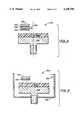
- FIG. 1shows a typical technique for chemi-mechanical polishing.
- a first disc-shaped pad 102having a layer of pressure sensitive adhesive 104 on its back face is adhered (i.e., mounted; shown exploded) to the front face of a rotating platen 106 (PLATEN).
- a second disc-shaped pad 108having a layer of pressure sensitive adhesive 110 on its back face is adhered (shown exploded) to the front face of the first pad 102.
- the platen 106is rotated (typically at tens of revolutions per minute), and a metered stream of slurry 112 (shown as dots) from a slurry supply 114 is delivered via a slurry feed 116 to the front face of PAD B.
- a silicon wafer 120is mounted to a carrier 122 and is lightly pressed (flat) against the front surface of PAD B so that irregular topographical formations (on the pad-confronting face of the wafer) sought to be polished are acted upon by the action of PAD B and the slurry.
- the pads 102 and 108 and the platen 106are on the order of 20-30 inches in diameter, the wafer is 4-6 inches in diameter, and polishing is performed in the center 2/3portion of PAD B.
- a reservoir 130contains the platen, pads, carrier, wafer and polishing slurry.
- Typical pad materialsare: (1) for PAD A, foamed polyurethane; and (2) for PAD B, felt fibrules (fibers), such as polyester felt, stiffened with polyurethane resin.
- PAD Bcan also be glass-impregnated plastic.
- the adhesive backings 104 and 110 for the padsare typically polyurethane based. Generally, it is preferable that PAD B is stiffer than PAD A. In the case that both pads are doped with polyurethane resin, this can be achieved simply by doping PAD B with more polyurethane than PAD A.
- Conditioning the padis a technique wherein the front face of the pad (e.g., PAD B) is "dressed", in a manner similar to dressing a grinding wheel.
- the general objectis that the wafer-confronting face of the pad being conditioned is made to be planar, prior to use.
- conditioningis performed “off-line”, in other words separate from the polishing process.
- polish ratesmay change by 20-50% during the lifetime of the pad, even with the best conditioning techniques. Such a variation introduces an undesirable variable into the polishing process.
- an ultrasonic transducerintroduces vibratory (mechanical) energy into the chemi-mechanical polishing process.
- the ultrasonic transduceris mounted to the platen upon which the pads are mounted.
- the ultrasonic transduceris mounted to carrier, to which the wafer being polished is mounted.
- the ultrasonic transduceris mounted to a carrier, to which the wafer being polished is mounted, and the carrier is resiliently mounted to allow for limited motion in the plane of the polishing pad.
- the transduceris simply mounted within the reservoir containing the polishing process, to vibrate the slurry.
- FIG. 1is an exploded, stylized, cross-sectional view of prior art chemi-mechanical polishing apparatus.
- FIG. 2is an exploded, stylized, cross-sectional view of the chemi-mechanical polishing apparatus of the present invention.
- FIG. 3is an exploded, stylized, cross-sectional view of the chemi-mechanical polishing apparatus of another embodiment of the present invention.
- FIG. 4is an exploded, stylized, cross-sectional view of the chemi-mechanical polishing apparatus of yet another embodiment of the present invention.
- FIG. 5is an exploded, stylized, cross-sectional view of the chemi-mechanical polishing apparatus of yet another embodiment of the present invention.
- FIG. 1shows chemi-mechanical polishing apparatus 100 of the prior art, and has been discussed above.
- chemi-mechanical polishingsuffers from low polish rates, poor repeatability and sensitivity to pad use history, and frequent conditioning of the pads "off-line" is required.
- chemi-mechanical polishingis the subject of ongoing inquiry, although some usable theories have evolved. Practitioners are in general agreement that the process is not strictly mechanical (abrasive) in nature, where grit in the polishing slurry simply knocks off elevated topological features on the wafer. It is also generally agreed that the process is not strictly chemical in nature, which would amount to a wet etching model. Some other, synergistic mechanism is likely active.
- a useful theory for chemi-mechanical polishingis that the chemical action of the polishing slurry creates a "sol" on the wafer surface being polished.
- a solis a highly hydrated material in a state just prior to going into solution.
- the theorycontinues that the mechanical action of polishing (pad rotation) may enhance sol creation by adding mechanical energy to the system, but almost certainly enhances removal of the sol from the surface of the wafer.
- the mechanical action of the suspended grit (silica, silica/cesium) particles in the slurry impacting the surface of the waferhas an effect.
- the present inventiondemonstrably improves upon existing chemi-mechanical polishing techniques.
- FIG. 2shows the chemi-mechanical polishing apparatus 200 of the present invention.
- a disc-shaped polishing pad 202which may be a composite pad (i.e., PAD A and PAD B) is mounted to a rotating platen 206.
- the platenhas a flat front surface 206a.
- the pad 202has a front face 202a oriented towards a wafer to be polished, and a back face 202b. The back face of the pad is mounted (typically adhered) to the front face of the platen.
- a silicon wafer 220is mounted to a carrier 222.
- the waferhas a front face 220a containing in-process and/or completed circuit structures (i.e., layers and circuit elements).
- the front face of the waferis oriented towards the front face of the pad.
- the platen surface 206a, pad face 202a and wafer face 220aare co-planar (but spaced apart).
- a slurryis introduced to the front face of the pad (see FIG. 1), and the wafer is urged (lightly pressed) against the pad. In this manner, irregular topographical features on the front face of the wafer are removed, and the front face of the wafer becomes planarized.
- a mechanical, vibratory, preferably ultrasonic (e.g., 15-30 kilohertz) transducer 250is mounted to the underside 206b of the platen.
- the transduceris energized during polishing, hence "on-line". This may be accomplished with suitable slip rings, or the like, providing electrical energy from a stationary source to the rotating platen.
- suitable slip rings, or the likeOne skilled in the art to which this invention most nearly pertains will readily understand how to energize the transducer.
- the platen/transducer combinationis preferably balanced. This may be accomplished by removing a suitable amount of material from the platen in the area of the transducer, or (as shown) by mounting a suitable counterweight 252 to the underside 206b of the platen at a location diametrically opposed to the transducer.
- the transducer 250is preferably oriented to establish a limited degree of pad motion (oscillation), in the plane of the platen, as illustrated by the two-headed arrow "v". Or, the transducer may be oriented to establish a limited degree of pad motion (oscillation) normal to the plane of the platen.
- the slurry itselfparticularly the grit in the slurry, will also become agitated.
- These pad motions, and the agitation of the slurryin any case, represent mechanical energy added to the system (in addition to the rotation of the platen) which improve polishing rates. It is also evident that the pad will be, to some extent, "self-conditioning" in that less frequent off-line conditioning of the pad is required.
- the frequency of the transduceris selected to be approximately two or more orders of magnitude (powers of ten) higher than the rotational frequency of the platen.
- the frequency of the transduceris on the order of tens of kilohertz, and the frequency of the platen is on the order of tens of hertz.
- the chemi-mechanical polishing process 200 described aboveis performed in a suitable reservoir with a suitable supply of slurry. Compare FIG. 1.
- FIG. 3shows an alternate embodiment 300 of the invention.
- the transducer 350(comparable to the transducer 250) is mounted to the wafer carrier 222. Since the wafer carrier does not rotate, it is a simple matter to energize the transducer 350. Again, the transducer introduces an additional, discrete mechanical energy into the system, which improves etch rate and repeatability, and which tends to self-condition the polishing pad. In this case, the wafer itself oscillates.
- the transduceris preferably oriented so that the wafer oscillates in the plane of the platen, as indicated by the two-headed arrow "v". However, the transducer can be oriented so that the wafer oscillates normal to the platen.
- the chemi-mechanical polishing process 300 described aboveis performed in a suitable reservoir with a suitable supply of slurry. Compare FIG. 1.
- FIG. 4shows another alternate embodiment 400 of the invention.
- the waferrather than the pad, is oscillated (vibrated) by the transducer.
- the wafer 220is mounted indirectly to a sub-carrier 424, which in turn is resiliently mounted to the carrier 422.
- a suitable resilient mountingis an elastomeric layer 426 disposed between the carrier 422 and the sub-carrier 424.
- This elastomeric mounting of the waferhas the advantage of preferably allowing movement (oscillation) of the wafer in the plane of the platen, due to the relatively low in-plane shear modulus of common elastomeric material.
- the transducer 450(comparable to 250, 350) is mounted to the side of the wafer carrier 422.
- the chemi-mechanical polishing process 400 described aboveis performed in a suitable reservoir with a suitable supply of slurry. Compare FIG. 1.
- FIG. 5shows yet another alternate embodiment 500 of the invention.
- the transducer 550is disposed in the system, at any suitable location, to agitate the slurry itself.
- the transducer 550(comparable to 250, 350, 450) is not mounted to the platen or to the carrier. As shown, the transducer 550 is mounted to an inner wall of the reservoir 530.
- chemi-mechanical polishingusually involves feeding slurry 112 to the face of the polishing pad, and letting the slurry run off, rather than accumulate.
- polish ratewill increase with this embodiment, in that the slurry itself is agitated, it is not expected to demonstrate the same degree of self-conditioning (of the pad) as in the other embodiments.
- polish rates and repeatabilityare enhanced. There is less sensitivity to pad use history. Less slurry may be consumed in the process.
- the vibratory motion of the pad relative to the wafercauses the pad to condition itself in-situ, or "on-line".
Landscapes
- Engineering & Computer Science (AREA)
- Mechanical Engineering (AREA)
- Chemical & Material Sciences (AREA)
- Ceramic Engineering (AREA)
- Inorganic Chemistry (AREA)
- Crystallography & Structural Chemistry (AREA)
- Materials Engineering (AREA)
- Metallurgy (AREA)
- Organic Chemistry (AREA)
- Mechanical Treatment Of Semiconductor (AREA)
- Finish Polishing, Edge Sharpening, And Grinding By Specific Grinding Devices (AREA)
- Grinding-Machine Dressing And Accessory Apparatuses (AREA)
Abstract
Description
The present invention relates to techniques for polishing semiconductor devices, more particularly to techniques of chemical-mechanical ("chemi-mechanical " or "chem-mech") polishing wafers.
Chemi-mechanical polishing of semiconductor wafers is useful, at various stages of device fabrication, for planarizing irregular top surface topography, inter alia. For example, in the process of fabricating modern semiconductor integrated circuits, it is necessary to form conductive lines or other structures above previously formed structures. However, prior structure formation often leaves the top surface topography of the silicon wafer highly irregular, with bumps, areas of unequal elevation, troughs, trenches and/or other surface irregularities. As a result of these irregularities, deposition of subsequent layers of materials could easily result in incomplete coverage, breaks in the deposited material, voids, etc., if it were deposited directly over the aforementioned highly irregular surfaces. If the irregularities are not alleviated at each major processing step, the top surface topography of the surface irregularities will tend to become even more irregular, causing further problems as layers stack up in further processing of the semiconductor structure.
Depending upon the type of materials used and their intended purposes, numerous undesirable characteristics are produced when these deposition irregularities occur. Incomplete coverage of an insulating oxide layer can lead to short circuits between metallization layers. Voids can trap air or processing gases, either contaminating further processing steps or simply lowering overall device reliability. Sharp points on conductors can result in unusual, undesirable field effects. In general, processing high density circuits over highly irregular structures can lead to very poor yield and/or device performance.
Consequently, it is desirable to effect some type of planarization, or flattening, of integrated circuit structures in order to facilitate the processing of multi-layer integrated circuits and to improve their yield, performance, and reliability. In fact, all of today's high-density integrated circuit fabrication techniques make use of some method of forming planarized structures at critical points in the fabrication process.
Planarization techniques generally fall into one of several categories: chemical/mechanical polishing techniques; leveling with a filler material then etching back in a controlled environment; and various reflow techniques. Etching techniques can include wet etching, dry or plasma etching, electro-polishing, and ion milling, among others. A few less common planarization techniques exist, such as direct deposition of material into a trench by condensing material from a gaseous phase in the presence of laser light. Most of the differences between modern planarization techniques exist in the points in processing that the different techniques are applied, and in which methods and materials are used.
The present invention is directed to chemi-mechanical polishing process, which generally involves "rubbing" a wafer with a polishing pad in a slurry containing both an abrasive and chemicals. Typical slurry chemistry is KOH (Potassium Hydroxide), having a pH of about 11. Generally, polishing slurry is expensive, and cannot be recovered or reused. A typical silica-based slurry is "SC-1" available from Cabot Industries. Another, more expensive slurry based on silica and cerium (oxide) is Rodel "WS-2000".
Chemi-mechanical polishing is described in U.S. Pat. Nos. 4,671,851, 4,910,155, 4,944,836, all of which patents are incorporated by reference herein. When chemi-mechanical polishing is referred to hereinafter, it should be understood to be performed with a suitable slurry, such as Cabot SC-1.
The current state of the art in dielectric film chemi-mechanical polishing for silicon wafers typically involves the use of more than one polishing pad. For example, two pads are secured into a "stack", which may be termed a "composite polishing pad". The top pad, which performs polishing, is typically stiffer than the more compliant bottom pad, which is mounted to a rotating platen. A pressure sensitive adhesive is typically used to adhere the pads together and to the platen.
FIG. 1. shows a typical technique for chemi-mechanical polishing. A first disc-shaped pad 102 (PAD A) having a layer of pressuresensitive adhesive 104 on its back face is adhered (i.e., mounted; shown exploded) to the front face of a rotating platen 106 (PLATEN). A second disc-shaped pad 108 (PAD B) having a layer of pressuresensitive adhesive 110 on its back face is adhered (shown exploded) to the front face of thefirst pad 102. Theplaten 106 is rotated (typically at tens of revolutions per minute), and a metered stream of slurry 112 (shown as dots) from aslurry supply 114 is delivered via a slurry feed 116 to the front face of PAD B.
Asilicon wafer 120 is mounted to acarrier 122 and is lightly pressed (flat) against the front surface of PAD B so that irregular topographical formations (on the pad-confronting face of the wafer) sought to be polished are acted upon by the action of PAD B and the slurry. Typically, thepads platen 106 are on the order of 20-30 inches in diameter, the wafer is 4-6 inches in diameter, and polishing is performed in the center 2/3portion of PAD B.
Areservoir 130 contains the platen, pads, carrier, wafer and polishing slurry.
Typical pad materials are: (1) for PAD A, foamed polyurethane; and (2) for PAD B, felt fibrules (fibers), such as polyester felt, stiffened with polyurethane resin. PAD B can also be glass-impregnated plastic. Theadhesive backings
Current chemi-mechanical polishing techniques suffer from low polish rates, poor repeatability, and sensitivity to pad use history. Pads must be "conditioned" prior to use, and during use the pads wear and change properties. The pads must be reconditioned after use, which only marginally improves polishing repeatability.
Conditioning the pad is a technique wherein the front face of the pad (e.g., PAD B) is "dressed", in a manner similar to dressing a grinding wheel. The general object is that the wafer-confronting face of the pad being conditioned is made to be planar, prior to use. Generally, such conditioning is performed "off-line", in other words separate from the polishing process.
Despite repeated conditioning of the polishing pads, polish rates may change by 20-50% during the lifetime of the pad, even with the best conditioning techniques. Such a variation introduces an undesirable variable into the polishing process.
It is an object of the present invention to provide improved techniques for chemi-mechanical polishing.
It is another object of the present invention to provide a technique for improving polish rate and repeatability.
It is another object of the present invention to provide a technique for reducing sensitivity to pad use history.
It is another object of the present invention to provide a technique for "on-line" conditioning of polishing pads.
According to the invention, an ultrasonic transducer introduces vibratory (mechanical) energy into the chemi-mechanical polishing process.
In one embodiment of the invention, the ultrasonic transducer is mounted to the platen upon which the pads are mounted.
In another embodiment of the invention, the ultrasonic transducer is mounted to carrier, to which the wafer being polished is mounted.
In yet another embodiment of the invention, the ultrasonic transducer is mounted to a carrier, to which the wafer being polished is mounted, and the carrier is resiliently mounted to allow for limited motion in the plane of the polishing pad.
In yet another embodiment of the invention, the transducer is simply mounted within the reservoir containing the polishing process, to vibrate the slurry.
Other objects, features and advantages of the present invention will become apparent in light of the following description thereof.
FIG. 1 is an exploded, stylized, cross-sectional view of prior art chemi-mechanical polishing apparatus.
FIG. 2 is an exploded, stylized, cross-sectional view of the chemi-mechanical polishing apparatus of the present invention.
FIG. 3 is an exploded, stylized, cross-sectional view of the chemi-mechanical polishing apparatus of another embodiment of the present invention.
FIG. 4 is an exploded, stylized, cross-sectional view of the chemi-mechanical polishing apparatus of yet another embodiment of the present invention.
FIG. 5 is an exploded, stylized, cross-sectional view of the chemi-mechanical polishing apparatus of yet another embodiment of the present invention.
FIG. 1 shows chemi-mechanical polishing apparatus 100 of the prior art, and has been discussed above.
As discussed above, chemi-mechanical polishing suffers from low polish rates, poor repeatability and sensitivity to pad use history, and frequent conditioning of the pads "off-line" is required.
The mechanism of chemi-mechanical polishing is the subject of ongoing inquiry, although some usable theories have evolved. Practitioners are in general agreement that the process is not strictly mechanical (abrasive) in nature, where grit in the polishing slurry simply knocks off elevated topological features on the wafer. It is also generally agreed that the process is not strictly chemical in nature, which would amount to a wet etching model. Some other, synergistic mechanism is likely active.
A useful theory for chemi-mechanical polishing is that the chemical action of the polishing slurry creates a "sol" on the wafer surface being polished. A sol is a highly hydrated material in a state just prior to going into solution. The theory continues that the mechanical action of polishing (pad rotation) may enhance sol creation by adding mechanical energy to the system, but almost certainly enhances removal of the sol from the surface of the wafer. Certainly, the mechanical action of the suspended grit (silica, silica/cesium) particles in the slurry impacting the surface of the wafer has an effect. Whatever the actual mechanism of chemi-mechanical polishing may be, the present invention demonstrably improves upon existing chemi-mechanical polishing techniques.
FIG. 2 shows the chemi-mechanical polishing apparatus 200 of the present invention.
In a manner consistent with the prior art, a disc-shapedpolishing pad 202, which may be a composite pad (i.e., PAD A and PAD B) is mounted to arotating platen 206. The platen has a flatfront surface 206a. Thepad 202 has a front face 202a oriented towards a wafer to be polished, and aback face 202b. The back face of the pad is mounted (typically adhered) to the front face of the platen.
In a manner consistent with the prior art, asilicon wafer 220 is mounted to acarrier 222. The wafer has a front face 220a containing in-process and/or completed circuit structures (i.e., layers and circuit elements). The front face of the wafer is oriented towards the front face of the pad. Theplaten surface 206a, pad face 202a and wafer face 220a are co-planar (but spaced apart).
In the process of chemi-mechanical polishing, a slurry is introduced to the front face of the pad (see FIG. 1), and the wafer is urged (lightly pressed) against the pad. In this manner, irregular topographical features on the front face of the wafer are removed, and the front face of the wafer becomes planarized.
According to an embodiment of the invention, a mechanical, vibratory, preferably ultrasonic (e.g., 15-30 kilohertz)transducer 250 is mounted to theunderside 206b of the platen. The transducer is energized during polishing, hence "on-line". This may be accomplished with suitable slip rings, or the like, providing electrical energy from a stationary source to the rotating platen. One skilled in the art to which this invention most nearly pertains will readily understand how to energize the transducer.
Since the platen rotates at tens of rpm (revolutions per minute), the platen/transducer combination is preferably balanced. This may be accomplished by removing a suitable amount of material from the platen in the area of the transducer, or (as shown) by mounting asuitable counterweight 252 to theunderside 206b of the platen at a location diametrically opposed to the transducer.
Thetransducer 250 is preferably oriented to establish a limited degree of pad motion (oscillation), in the plane of the platen, as illustrated by the two-headed arrow "v". Or, the transducer may be oriented to establish a limited degree of pad motion (oscillation) normal to the plane of the platen. In either case, the slurry itself, particularly the grit in the slurry, will also become agitated. These pad motions, and the agitation of the slurry, in any case, represent mechanical energy added to the system (in addition to the rotation of the platen) which improve polishing rates. It is also evident that the pad will be, to some extent, "self-conditioning" in that less frequent off-line conditioning of the pad is required. This is due, in part, to the fact that the frequency of the transducer is selected to be approximately two or more orders of magnitude (powers of ten) higher than the rotational frequency of the platen. In the example given above, the frequency of the transducer is on the order of tens of kilohertz, and the frequency of the platen is on the order of tens of hertz.
The chemi-mechanical polishing process 200 described above is performed in a suitable reservoir with a suitable supply of slurry. Compare FIG. 1.
FIG. 3 shows analternate embodiment 300 of the invention. In this case, the transducer 350 (comparable to the transducer 250) is mounted to thewafer carrier 222. Since the wafer carrier does not rotate, it is a simple matter to energize the transducer 350. Again, the transducer introduces an additional, discrete mechanical energy into the system, which improves etch rate and repeatability, and which tends to self-condition the polishing pad. In this case, the wafer itself oscillates. Again, the transducer is preferably oriented so that the wafer oscillates in the plane of the platen, as indicated by the two-headed arrow "v". However, the transducer can be oriented so that the wafer oscillates normal to the platen.
The chemi-mechanical polishing process 300 described above is performed in a suitable reservoir with a suitable supply of slurry. Compare FIG. 1.
FIG. 4 shows anotheralternate embodiment 400 of the invention. As with the embodiment of FIG. 3, the wafer, rather than the pad, is oscillated (vibrated) by the transducer. However, in this case, thewafer 220 is mounted indirectly to asub-carrier 424, which in turn is resiliently mounted to the carrier 422. A suitable resilient mounting is anelastomeric layer 426 disposed between the carrier 422 and thesub-carrier 424. This elastomeric mounting of the wafer has the advantage of preferably allowing movement (oscillation) of the wafer in the plane of the platen, due to the relatively low in-plane shear modulus of common elastomeric material.
In this embodiment, the transducer 450 (comparable to 250, 350) is mounted to the side of the wafer carrier 422.
The chemi-mechanical polishing process 400 described above is performed in a suitable reservoir with a suitable supply of slurry. Compare FIG. 1.
FIG. 5 shows yet anotheralternate embodiment 500 of the invention. In this case, thetransducer 550 is disposed in the system, at any suitable location, to agitate the slurry itself. The transducer 550 (comparable to 250, 350, 450) is not mounted to the platen or to the carrier. As shown, thetransducer 550 is mounted to an inner wall of thereservoir 530.
This is perhaps the simplest of the embodiments, in that the fewest modifications to existing systems are involved. However, this embodiment requires that the reservoir fill substantially with slurry, which is not the common mode of chemi-mechanical polishing. As shown more clearly in FIG. 1, chemi-mechanical polishing usually involves feedingslurry 112 to the face of the polishing pad, and letting the slurry run off, rather than accumulate.
While it is expected that polish rate will increase with this embodiment, in that the slurry itself is agitated, it is not expected to demonstrate the same degree of self-conditioning (of the pad) as in the other embodiments.
The disclosed techniques of introducing mechanical vibratory energy into the chemi-mechanical polishing system has been demonstrated to be useful in polishing oxide and glass layers on silicon wafers, and would appear to be useful in polishing tungsten films and other semiconductor structures. Polish rates and repeatability are enhanced. There is less sensitivity to pad use history. Less slurry may be consumed in the process.
In the embodiments of FIGS. 2, 3 and 4, the vibratory motion of the pad relative to the wafer (and vice-versa), causes the pad to condition itself in-situ, or "on-line".
Claims (5)
1. Apparatus for chemi-mechanical polishing of semiconductor wafers, comprising:
a rotating platen having a planar front face;
at least one polishing pad mounted to the front face of the platen and rotating with the platen; the pad having a front face for polishing a wafer;
means for delivering slurry to the front face of the pad;
a carrier having a front surface facing the polishing pad, and a back surface facing away from the polishing pad;
means for mounting a wafer to the pad-facing surface of the carrier; and
means for causing relative vibration between the pad and the wafer;
further comprising;
a sub-carrier having a surface facing the back surface of the carrier; and
an elastomeric layer interposed between the back surface of the carrier-facing surface of the sub-carrier for allowing movement of the wafer in the plane of the carrier;
wherein;
the means for vibrating is an ultrasonic transducer mounted to the carrier.
2. Apparatus, according the claim 1, wherein:
the transducer is oriented to vibrate the wafer in the plane of the platen.
3. Apparatus, according to claim 1, wherein:
the platen rotates at a first frequency;
the means for vibrating is a transducer vibrating at a second frequency; and
the second frequency is two or more orders of magnitude greater that the first frequency.
4. Apparatus according to claim 1, wherein:
two polishing pads are provided, a first polishing pad adhered to the platen and a second polishing pad adhered to the first polishing pad.
5. Apparatus according to claim 4, wherein:
the second polishing pad is stiffer than the first polishing pad.
Priority Applications (3)
| Application Number | Priority Date | Filing Date | Title |
|---|---|---|---|
| US07/837,444US5245790A (en) | 1992-02-14 | 1992-02-14 | Ultrasonic energy enhanced chemi-mechanical polishing of silicon wafers |
| JP4450093AJPH0621029A (en) | 1992-02-14 | 1993-02-09 | Apparatus and method for chemical- mechanical polishing of semiconductor wafer |
| DE4304429ADE4304429A1 (en) | 1992-02-14 | 1993-02-14 |
Applications Claiming Priority (1)
| Application Number | Priority Date | Filing Date | Title |
|---|---|---|---|
| US07/837,444US5245790A (en) | 1992-02-14 | 1992-02-14 | Ultrasonic energy enhanced chemi-mechanical polishing of silicon wafers |
Publications (1)
| Publication Number | Publication Date |
|---|---|
| US5245790Atrue US5245790A (en) | 1993-09-21 |
Family
ID=25274456
Family Applications (1)
| Application Number | Title | Priority Date | Filing Date |
|---|---|---|---|
| US07/837,444Expired - LifetimeUS5245790A (en) | 1992-02-14 | 1992-02-14 | Ultrasonic energy enhanced chemi-mechanical polishing of silicon wafers |
Country Status (3)
| Country | Link |
|---|---|
| US (1) | US5245790A (en) |
| JP (1) | JPH0621029A (en) |
| DE (1) | DE4304429A1 (en) |
Cited By (115)
| Publication number | Priority date | Publication date | Assignee | Title |
|---|---|---|---|---|
| US5522965A (en)* | 1994-12-12 | 1996-06-04 | Texas Instruments Incorporated | Compact system and method for chemical-mechanical polishing utilizing energy coupled to the polishing pad/water interface |
| US5527423A (en)* | 1994-10-06 | 1996-06-18 | Cabot Corporation | Chemical mechanical polishing slurry for metal layers |
| US5551907A (en)* | 1994-03-14 | 1996-09-03 | Hughes Aircraft Company | System for ultrasonic lap grinding and polishing |
| US5562530A (en)* | 1994-08-02 | 1996-10-08 | Sematech, Inc. | Pulsed-force chemical mechanical polishing |
| US5607341A (en) | 1994-08-08 | 1997-03-04 | Leach; Michael A. | Method and structure for polishing a wafer during manufacture of integrated circuits |
| US5624304A (en)* | 1992-07-10 | 1997-04-29 | Lsi Logic, Inc. | Techniques for assembling polishing pads for chemi-mechanical polishing of silicon wafers |
| US5688364A (en)* | 1994-12-22 | 1997-11-18 | Sony Corporation | Chemical-mechanical polishing method and apparatus using ultrasound applied to the carrier and platen |
| US5733175A (en) | 1994-04-25 | 1998-03-31 | Leach; Michael A. | Polishing a workpiece using equal velocity at all points overlapping a polisher |
| US5772780A (en)* | 1994-09-30 | 1998-06-30 | Hitachi, Ltd. | Polishing agent and polishing method |
| US5783497A (en)* | 1994-08-02 | 1998-07-21 | Sematech, Inc. | Forced-flow wafer polisher |
| US5868608A (en)* | 1996-08-13 | 1999-02-09 | Lsi Logic Corporation | Subsonic to supersonic and ultrasonic conditioning of a polishing pad in a chemical mechanical polishing apparatus |
| EP0849778A3 (en)* | 1996-12-19 | 1999-03-31 | Texas Instruments Incorporated | Improvements in or relating to wafer polishing |
| US5890951A (en)* | 1996-04-15 | 1999-04-06 | Lsi Logic Corporation | Utility wafer for chemical-mechanical planarization |
| US5895550A (en)* | 1996-12-16 | 1999-04-20 | Micron Technology, Inc. | Ultrasonic processing of chemical mechanical polishing slurries |
| US5899801A (en)* | 1996-10-31 | 1999-05-04 | Applied Materials, Inc. | Method and apparatus for removing a substrate from a polishing pad in a chemical mechanical polishing system |
| US5913712A (en)* | 1995-08-09 | 1999-06-22 | Cypress Semiconductor Corp. | Scratch reduction in semiconductor circuit fabrication using chemical-mechanical polishing |
| US5945347A (en)* | 1995-06-02 | 1999-08-31 | Micron Technology, Inc. | Apparatus and method for polishing a semiconductor wafer in an overhanging position |
| US5957754A (en)* | 1997-08-29 | 1999-09-28 | Applied Materials, Inc. | Cavitational polishing pad conditioner |
| US5967881A (en)* | 1997-05-29 | 1999-10-19 | Tucker; Thomas N. | Chemical mechanical planarization tool having a linear polishing roller |
| US5968851A (en)* | 1997-03-19 | 1999-10-19 | Cypress Semiconductor Corp. | Controlled isotropic etch process and method of forming an opening in a dielectric layer |
| US5968841A (en)* | 1997-05-06 | 1999-10-19 | International Business Machines Corporation | Device and method for preventing settlement of particles on a chemical-mechanical polishing pad |
| US5975994A (en)* | 1997-06-11 | 1999-11-02 | Micron Technology, Inc. | Method and apparatus for selectively conditioning a polished pad used in planarizng substrates |
| US6024829A (en)* | 1998-05-21 | 2000-02-15 | Lucent Technologies Inc. | Method of reducing agglomerate particles in a polishing slurry |
| US6060370A (en)* | 1998-06-16 | 2000-05-09 | Lsi Logic Corporation | Method for shallow trench isolations with chemical-mechanical polishing |
| US6066266A (en)* | 1998-07-08 | 2000-05-23 | Lsi Logic Corporation | In-situ chemical-mechanical polishing slurry formulation for compensation of polish pad degradation |
| US6071818A (en)* | 1998-06-30 | 2000-06-06 | Lsi Logic Corporation | Endpoint detection method and apparatus which utilize an endpoint polishing layer of catalyst material |
| US6074517A (en)* | 1998-07-08 | 2000-06-13 | Lsi Logic Corporation | Method and apparatus for detecting an endpoint polishing layer by transmitting infrared light signals through a semiconductor wafer |
| US6077783A (en)* | 1998-06-30 | 2000-06-20 | Lsi Logic Corporation | Method and apparatus for detecting a polishing endpoint based upon heat conducted through a semiconductor wafer |
| US6080670A (en)* | 1998-08-10 | 2000-06-27 | Lsi Logic Corporation | Method of detecting a polishing endpoint layer of a semiconductor wafer which includes a non-reactive reporting specie |
| US6080042A (en)* | 1997-10-31 | 2000-06-27 | Virginia Semiconductor, Inc. | Flatness and throughput of single side polishing of wafers |
| US6093280A (en)* | 1997-08-18 | 2000-07-25 | Lsi Logic Corporation | Chemical-mechanical polishing pad conditioning systems |
| US6106371A (en)* | 1997-10-30 | 2000-08-22 | Lsi Logic Corporation | Effective pad conditioning |
| US6108093A (en)* | 1997-06-04 | 2000-08-22 | Lsi Logic Corporation | Automated inspection system for residual metal after chemical-mechanical polishing |
| US6115233A (en)* | 1996-06-28 | 2000-09-05 | Lsi Logic Corporation | Integrated circuit device having a capacitor with the dielectric peripheral region being greater than the dielectric central region |
| US6117779A (en)* | 1998-12-15 | 2000-09-12 | Lsi Logic Corporation | Endpoint detection method and apparatus which utilize a chelating agent to detect a polishing endpoint |
| US6121147A (en)* | 1998-12-11 | 2000-09-19 | Lsi Logic Corporation | Apparatus and method of detecting a polishing endpoint layer of a semiconductor wafer which includes a metallic reporting substance |
| US6124207A (en)* | 1998-08-31 | 2000-09-26 | Micron Technology, Inc. | Slurries for mechanical or chemical-mechanical planarization of microelectronic-device substrate assemblies, and methods and apparatuses for making and using such slurries |
| US6135863A (en)* | 1999-04-20 | 2000-10-24 | Memc Electronic Materials, Inc. | Method of conditioning wafer polishing pads |
| US6168508B1 (en) | 1997-08-25 | 2001-01-02 | Lsi Logic Corporation | Polishing pad surface for improved process control |
| US6179956B1 (en) | 1998-01-09 | 2001-01-30 | Lsi Logic Corporation | Method and apparatus for using across wafer back pressure differentials to influence the performance of chemical mechanical polishing |
| US6201253B1 (en) | 1998-10-22 | 2001-03-13 | Lsi Logic Corporation | Method and apparatus for detecting a planarized outer layer of a semiconductor wafer with a confocal optical system |
| US6234883B1 (en) | 1997-10-01 | 2001-05-22 | Lsi Logic Corporation | Method and apparatus for concurrent pad conditioning and wafer buff in chemical mechanical polishing |
| US6241847B1 (en) | 1998-06-30 | 2001-06-05 | Lsi Logic Corporation | Method and apparatus for detecting a polishing endpoint based upon infrared signals |
| US6264532B1 (en)* | 2000-03-28 | 2001-07-24 | Speedfam-Ipec Corporation | Ultrasonic methods and apparatus for the in-situ detection of workpiece loss |
| US6268224B1 (en) | 1998-06-30 | 2001-07-31 | Lsi Logic Corporation | Method and apparatus for detecting an ion-implanted polishing endpoint layer within a semiconductor wafer |
| US6276842B1 (en)* | 1997-12-16 | 2001-08-21 | The Furukawa Electric Co. Ltd. | Optical component, method for polishing the end faces of optical component, and apparatus for polishing the same |
| US6285035B1 (en) | 1998-07-08 | 2001-09-04 | Lsi Logic Corporation | Apparatus for detecting an endpoint polishing layer of a semiconductor wafer having a wafer carrier with independent concentric sub-carriers and associated method |
| US6297558B1 (en) | 1997-07-23 | 2001-10-02 | Lsi Logic Corporation | Slurry filling a recess formed during semiconductor fabrication |
| US6340434B1 (en) | 1997-09-05 | 2002-01-22 | Lsi Logic Corporation | Method and apparatus for chemical-mechanical polishing |
| US6350691B1 (en)* | 1997-12-22 | 2002-02-26 | Micron Technology, Inc. | Method and apparatus for planarizing microelectronic substrates and conditioning planarizing media |
| US6372524B1 (en) | 2001-03-06 | 2002-04-16 | Lsi Logic Corporation | Method for CMP endpoint detection |
| US6375550B1 (en) | 2000-06-05 | 2002-04-23 | Lsi Logic Corporation | Method and apparatus for enhancing uniformity during polishing of a semiconductor wafer |
| US6406364B1 (en) | 1997-08-12 | 2002-06-18 | Ebara Corporation | Polishing solution feeder |
| US6451699B1 (en) | 1999-07-30 | 2002-09-17 | Lsi Logic Corporation | Method and apparatus for planarizing a wafer surface of a semiconductor wafer having an elevated portion extending therefrom |
| US6464566B1 (en) | 2000-06-29 | 2002-10-15 | Lsi Logic Corporation | Apparatus and method for linearly planarizing a surface of a semiconductor wafer |
| US6503828B1 (en) | 2001-06-14 | 2003-01-07 | Lsi Logic Corporation | Process for selective polishing of metal-filled trenches of integrated circuit structures |
| US6511576B2 (en) | 1999-11-17 | 2003-01-28 | Micron Technology, Inc. | System for planarizing microelectronic substrates having apertures |
| US6528389B1 (en) | 1998-12-17 | 2003-03-04 | Lsi Logic Corporation | Substrate planarization with a chemical mechanical polishing stop layer |
| US6533893B2 (en) | 1999-09-02 | 2003-03-18 | Micron Technology, Inc. | Method and apparatus for chemical-mechanical planarization of microelectronic substrates with selected planarizing liquids |
| US6541383B1 (en) | 2000-06-29 | 2003-04-01 | Lsi Logic Corporation | Apparatus and method for planarizing the surface of a semiconductor wafer |
| US6548407B1 (en) | 2000-04-26 | 2003-04-15 | Micron Technology, Inc. | Method and apparatus for controlling chemical interactions during planarization of microelectronic substrates |
| US6554688B2 (en) | 2001-01-04 | 2003-04-29 | Lam Research Corporation | Method and apparatus for conditioning a polishing pad with sonic energy |
| US6555475B1 (en)* | 2000-12-28 | 2003-04-29 | Lsi Logic Corporation | Arrangement and method for polishing a surface of a semiconductor wafer |
| US6666749B2 (en) | 2001-08-30 | 2003-12-23 | Micron Technology, Inc. | Apparatus and method for enhanced processing of microelectronic workpieces |
| US20040029490A1 (en)* | 2000-06-07 | 2004-02-12 | Agarwal Vishnu K. | Apparatuses and methods for in-situ optical endpointing on web-format planarizing machines in mechanical or chemical-mechanical planarization of microelectronic-device substrate assemblies |
| US20040038623A1 (en)* | 2002-08-26 | 2004-02-26 | Nagasubramaniyan Chandrasekaran | Methods and systems for conditioning planarizing pads used in planarizing substrates |
| US20040041556A1 (en)* | 2002-08-29 | 2004-03-04 | Martin Michael H. | Planarity diagnostic system, E.G., for microelectronic component test systems |
| US20040043699A1 (en)* | 2002-08-29 | 2004-03-04 | Nagasubramaniyan Chandrasekaran | Apparatus and method for mechanical and/or chemical-mechanical planarization of micro-device workpieces |
| US6705930B2 (en) | 2000-01-28 | 2004-03-16 | Lam Research Corporation | System and method for polishing and planarizing semiconductor wafers using reduced surface area polishing pads and variable partial pad-wafer overlapping techniques |
| US6722943B2 (en) | 2001-08-24 | 2004-04-20 | Micron Technology, Inc. | Planarizing machines and methods for dispensing planarizing solutions in the processing of microelectronic workpieces |
| US6729943B2 (en) | 2000-01-28 | 2004-05-04 | Lam Research Corporation | System and method for controlled polishing and planarization of semiconductor wafers |
| US20040092106A1 (en)* | 2002-11-12 | 2004-05-13 | Nicholas Martyak | Copper chemical mechanical polishing solutions using sulfonated amphiprotic agents |
| US20040116313A1 (en)* | 2002-12-02 | 2004-06-17 | Martin Nosowitz | Composition and method for copper chemical mechanical planarization |
| US6833046B2 (en) | 2000-05-04 | 2004-12-21 | Micron Technology, Inc. | Planarizing machines and methods for mechanical and/or chemical-mechanical planarization of microelectronic-device substrate assemblies |
| US20050014457A1 (en)* | 2001-08-24 | 2005-01-20 | Taylor Theodore M. | Apparatus and method for conditioning a contact surface of a processing pad used in processing microelectronic workpieces |
| US20050026555A1 (en)* | 2002-08-08 | 2005-02-03 | Terry Castor | Carrier assemblies, planarizing apparatuses including carrier assemblies, and methods for planarizing micro-device workpieces |
| US20050037694A1 (en)* | 2002-07-08 | 2005-02-17 | Taylor Theodore M. | Retaining rings, planarizing apparatuses including retaining rings, and methods for planarizing micro-device workpieces |
| US6872132B2 (en) | 2003-03-03 | 2005-03-29 | Micron Technology, Inc. | Systems and methods for monitoring characteristics of a polishing pad used in polishing micro-device workpieces |
| US6875091B2 (en)* | 2001-01-04 | 2005-04-05 | Lam Research Corporation | Method and apparatus for conditioning a polishing pad with sonic energy |
| US6884152B2 (en) | 2003-02-11 | 2005-04-26 | Micron Technology, Inc. | Apparatuses and methods for conditioning polishing pads used in polishing micro-device workpieces |
| US6935929B2 (en) | 2003-04-28 | 2005-08-30 | Micron Technology, Inc. | Polishing machines including under-pads and methods for mechanical and/or chemical-mechanical polishing of microfeature workpieces |
| US6958001B2 (en) | 2002-08-23 | 2005-10-25 | Micron Technology, Inc. | Carrier assemblies, planarizing apparatuses including carrier assemblies, and methods for planarizing micro-device workpieces |
| US6964924B1 (en) | 2001-09-11 | 2005-11-15 | Lsi Logic Corporation | Integrated circuit process monitoring and metrology system |
| US6969306B2 (en) | 2002-03-04 | 2005-11-29 | Micron Technology, Inc. | Apparatus for planarizing microelectronic workpieces |
| US7030603B2 (en) | 2003-08-21 | 2006-04-18 | Micron Technology, Inc. | Apparatuses and methods for monitoring rotation of a conductive microfeature workpiece |
| US7033253B2 (en) | 2004-08-12 | 2006-04-25 | Micron Technology, Inc. | Polishing pad conditioners having abrasives and brush elements, and associated systems and methods |
| US7033251B2 (en) | 2003-01-16 | 2006-04-25 | Micron Technology, Inc. | Carrier assemblies, polishing machines including carrier assemblies, and methods for polishing micro-device workpieces |
| US7066792B2 (en) | 2004-08-06 | 2006-06-27 | Micron Technology, Inc. | Shaped polishing pads for beveling microfeature workpiece edges, and associate system and methods |
| US7086927B2 (en) | 2004-03-09 | 2006-08-08 | Micron Technology, Inc. | Methods and systems for planarizing workpieces, e.g., microelectronic workpieces |
| US7094695B2 (en) | 2002-08-21 | 2006-08-22 | Micron Technology, Inc. | Apparatus and method for conditioning a polishing pad used for mechanical and/or chemical-mechanical planarization |
| US7131891B2 (en) | 2003-04-28 | 2006-11-07 | Micron Technology, Inc. | Systems and methods for mechanical and/or chemical-mechanical polishing of microfeature workpieces |
| US7182669B2 (en) | 2002-07-18 | 2007-02-27 | Micron Technology, Inc. | Methods and systems for planarizing workpieces, e.g., microelectronic workpieces |
| US20070049172A1 (en)* | 2005-08-31 | 2007-03-01 | Micron Technology, Inc. | Apparatus and method for removing material from microfeature workpieces |
| US20070077871A1 (en)* | 2005-07-28 | 2007-04-05 | Moo-Yong Park | Chemical mechanical polishing devices, pad conditioner assembly and polishing pad conditioning method thereof |
| US20070163677A1 (en)* | 2003-04-10 | 2007-07-19 | Yair Ein-Eli | Copper cmp slurry composition |
| US7264539B2 (en) | 2005-07-13 | 2007-09-04 | Micron Technology, Inc. | Systems and methods for removing microfeature workpiece surface defects |
| US7294049B2 (en) | 2005-09-01 | 2007-11-13 | Micron Technology, Inc. | Method and apparatus for removing material from microfeature workpieces |
| US7326105B2 (en) | 2005-08-31 | 2008-02-05 | Micron Technology, Inc. | Retaining rings, and associated planarizing apparatuses, and related methods for planarizing micro-device workpieces |
| US20090127231A1 (en)* | 2007-11-08 | 2009-05-21 | Chien-Min Sung | Methods of Forming Superhard Cutters and Superhard Cutters Formed Thereby |
| US20100132687A1 (en)* | 2007-01-16 | 2010-06-03 | John Budiac | Adjustable material cutting guide system |
| US7751609B1 (en) | 2000-04-20 | 2010-07-06 | Lsi Logic Corporation | Determination of film thickness during chemical mechanical polishing |
| US7754612B2 (en) | 2007-03-14 | 2010-07-13 | Micron Technology, Inc. | Methods and apparatuses for removing polysilicon from semiconductor workpieces |
| US20110003538A1 (en)* | 2006-02-06 | 2011-01-06 | Chien-Min Sung | Pad Conditioner Dresser |
| CN102179732A (en)* | 2009-12-31 | 2011-09-14 | 宋健民 | Chemical mechanical polishing system and related method |
| US8142261B1 (en)* | 2006-11-27 | 2012-03-27 | Chien-Min Sung | Methods for enhancing chemical mechanical polishing pad processes |
| CN103802018A (en)* | 2012-11-01 | 2014-05-21 | 罗门哈斯电子材料Cmp控股股份有限公司 | Soft and conditionable chemical mechanical polishing pad |
| US20140220864A1 (en)* | 2013-02-05 | 2014-08-07 | Ebara Corporation | Polishing apparatus |
| US20140357163A1 (en)* | 2013-05-31 | 2014-12-04 | Dow Global Technologies Llc | Multilayer Chemical Mechanical Polishing Pad Stack With Soft And Conditionable Polishing Layer |
| US20140357169A1 (en)* | 2013-05-31 | 2014-12-04 | Dow Global Technologies Llc | Soft And Conditionable Chemical Mechanical Polishing Pad Stack |
| CN104416453A (en)* | 2013-08-30 | 2015-03-18 | 罗门哈斯电子材料Cmp控股股份有限公司 | Method of chemical mechanical polishing a substrate |
| CN105014528A (en)* | 2014-04-25 | 2015-11-04 | 陶氏环球技术有限公司 | Chemical mechanical polishing pad |
| CN107363649A (en)* | 2017-08-08 | 2017-11-21 | 北京交通大学 | A kind of electrostriction ultrasonic vibration burnishing device |
| US10199242B2 (en) | 2014-12-31 | 2019-02-05 | Osaka University | Planarizing processing method and planarizing processing device |
| US10770301B2 (en) | 2016-03-11 | 2020-09-08 | Toho Engineering Co., Ltd. | Planarization processing device |
| CN114310627A (en)* | 2021-12-30 | 2022-04-12 | 西安奕斯伟材料科技有限公司 | Polishing pad and polishing equipment for polishing silicon wafer |
Families Citing this family (7)
| Publication number | Priority date | Publication date | Assignee | Title |
|---|---|---|---|---|
| US5245796A (en)* | 1992-04-02 | 1993-09-21 | At&T Bell Laboratories | Slurry polisher using ultrasonic agitation |
| EP0779655A3 (en)* | 1995-12-14 | 1997-07-16 | International Business Machines Corporation | A method of chemically-mechanically polishing an electronic component |
| JPH09185095A (en)* | 1995-12-28 | 1997-07-15 | Olympus Optical Co Ltd | Image pickup device |
| DE19928950A1 (en)* | 1999-06-24 | 2000-12-07 | Wacker Siltronic Halbleitermat | Semiconductor disc surface polishing method has perpendicular oscillating movement superimposed on relative displacement of rotary polishing tool and rotating semiconductor disc |
| DE10060696A1 (en)* | 2000-12-07 | 2002-06-27 | Wacker Chemie Gmbh | Method by which edges of brittle hard materials may be ground has the tool subjected to ultrasonic frequencies |
| CN102962756B (en)* | 2012-12-12 | 2015-01-21 | 天津中环领先材料技术有限公司 | Monocrystal silicon wafer polishing process capable of obtaining high polishing rate |
| CN113118966B (en)* | 2019-12-31 | 2022-08-16 | 清华大学 | Bearing head for chemical mechanical polishing and using method thereof |
Citations (10)
| Publication number | Priority date | Publication date | Assignee | Title |
|---|---|---|---|---|
| US2967381A (en)* | 1958-04-07 | 1961-01-10 | Bendix Corp | Means for cutting |
| US3093937A (en)* | 1962-11-30 | 1963-06-18 | Cavitron Ultrasonics Inc | Ultrasonic lapping machines |
| US3841031A (en)* | 1970-10-21 | 1974-10-15 | Monsanto Co | Process for polishing thin elements |
| US4258508A (en)* | 1979-09-04 | 1981-03-31 | Rca Corporation | Free hold down of wafers for material removal |
| US4519168A (en)* | 1979-09-18 | 1985-05-28 | Speedfam Corporation | Liquid waxless fixturing of microsize wafers |
| US4671851A (en)* | 1985-10-28 | 1987-06-09 | International Business Machines Corporation | Method for removing protuberances at the surface of a semiconductor wafer using a chem-mech polishing technique |
| US4910155A (en)* | 1988-10-28 | 1990-03-20 | International Business Machines Corporation | Wafer flood polishing |
| US4944836A (en)* | 1985-10-28 | 1990-07-31 | International Business Machines Corporation | Chem-mech polishing method for producing coplanar metal/insulator films on a substrate |
| US5036015A (en)* | 1990-09-24 | 1991-07-30 | Micron Technology, Inc. | Method of endpoint detection during chemical/mechanical planarization of semiconductor wafers |
| US5165205A (en)* | 1987-06-24 | 1992-11-24 | Research Development Corporation Of Japan | Device for vibrating materials to be ground |
- 1992
- 1992-02-14USUS07/837,444patent/US5245790A/ennot_activeExpired - Lifetime
- 1993
- 1993-02-09JPJP4450093Apatent/JPH0621029A/ennot_activeWithdrawn
- 1993-02-14DEDE4304429Apatent/DE4304429A1/denot_activeWithdrawn
Patent Citations (10)
| Publication number | Priority date | Publication date | Assignee | Title |
|---|---|---|---|---|
| US2967381A (en)* | 1958-04-07 | 1961-01-10 | Bendix Corp | Means for cutting |
| US3093937A (en)* | 1962-11-30 | 1963-06-18 | Cavitron Ultrasonics Inc | Ultrasonic lapping machines |
| US3841031A (en)* | 1970-10-21 | 1974-10-15 | Monsanto Co | Process for polishing thin elements |
| US4258508A (en)* | 1979-09-04 | 1981-03-31 | Rca Corporation | Free hold down of wafers for material removal |
| US4519168A (en)* | 1979-09-18 | 1985-05-28 | Speedfam Corporation | Liquid waxless fixturing of microsize wafers |
| US4671851A (en)* | 1985-10-28 | 1987-06-09 | International Business Machines Corporation | Method for removing protuberances at the surface of a semiconductor wafer using a chem-mech polishing technique |
| US4944836A (en)* | 1985-10-28 | 1990-07-31 | International Business Machines Corporation | Chem-mech polishing method for producing coplanar metal/insulator films on a substrate |
| US5165205A (en)* | 1987-06-24 | 1992-11-24 | Research Development Corporation Of Japan | Device for vibrating materials to be ground |
| US4910155A (en)* | 1988-10-28 | 1990-03-20 | International Business Machines Corporation | Wafer flood polishing |
| US5036015A (en)* | 1990-09-24 | 1991-07-30 | Micron Technology, Inc. | Method of endpoint detection during chemical/mechanical planarization of semiconductor wafers |
Cited By (210)
| Publication number | Priority date | Publication date | Assignee | Title |
|---|---|---|---|---|
| US5624304A (en)* | 1992-07-10 | 1997-04-29 | Lsi Logic, Inc. | Techniques for assembling polishing pads for chemi-mechanical polishing of silicon wafers |
| US5551907A (en)* | 1994-03-14 | 1996-09-03 | Hughes Aircraft Company | System for ultrasonic lap grinding and polishing |
| US5733175A (en) | 1994-04-25 | 1998-03-31 | Leach; Michael A. | Polishing a workpiece using equal velocity at all points overlapping a polisher |
| US5783497A (en)* | 1994-08-02 | 1998-07-21 | Sematech, Inc. | Forced-flow wafer polisher |
| US5562530A (en)* | 1994-08-02 | 1996-10-08 | Sematech, Inc. | Pulsed-force chemical mechanical polishing |
| US5607341A (en) | 1994-08-08 | 1997-03-04 | Leach; Michael A. | Method and structure for polishing a wafer during manufacture of integrated circuits |
| US5702290A (en) | 1994-08-08 | 1997-12-30 | Leach; Michael A. | Block for polishing a wafer during manufacture of integrated circuits |
| US5836807A (en) | 1994-08-08 | 1998-11-17 | Leach; Michael A. | Method and structure for polishing a wafer during manufacture of integrated circuits |
| US5772780A (en)* | 1994-09-30 | 1998-06-30 | Hitachi, Ltd. | Polishing agent and polishing method |
| US6043155A (en)* | 1994-09-30 | 2000-03-28 | Hitachi, Ltd. | Polishing agent and polishing method |
| US5527423A (en)* | 1994-10-06 | 1996-06-18 | Cabot Corporation | Chemical mechanical polishing slurry for metal layers |
| US5522965A (en)* | 1994-12-12 | 1996-06-04 | Texas Instruments Incorporated | Compact system and method for chemical-mechanical polishing utilizing energy coupled to the polishing pad/water interface |
| US5688364A (en)* | 1994-12-22 | 1997-11-18 | Sony Corporation | Chemical-mechanical polishing method and apparatus using ultrasound applied to the carrier and platen |
| US6251785B1 (en) | 1995-06-02 | 2001-06-26 | Micron Technology, Inc. | Apparatus and method for polishing a semiconductor wafer in an overhanging position |
| US5945347A (en)* | 1995-06-02 | 1999-08-31 | Micron Technology, Inc. | Apparatus and method for polishing a semiconductor wafer in an overhanging position |
| US5913712A (en)* | 1995-08-09 | 1999-06-22 | Cypress Semiconductor Corp. | Scratch reduction in semiconductor circuit fabrication using chemical-mechanical polishing |
| US5890951A (en)* | 1996-04-15 | 1999-04-06 | Lsi Logic Corporation | Utility wafer for chemical-mechanical planarization |
| US6115233A (en)* | 1996-06-28 | 2000-09-05 | Lsi Logic Corporation | Integrated circuit device having a capacitor with the dielectric peripheral region being greater than the dielectric central region |
| US6168502B1 (en) | 1996-08-13 | 2001-01-02 | Lsi Logic Corporation | Subsonic to supersonic and ultrasonic conditioning of a polishing pad in a chemical mechanical polishing apparatus |
| US5868608A (en)* | 1996-08-13 | 1999-02-09 | Lsi Logic Corporation | Subsonic to supersonic and ultrasonic conditioning of a polishing pad in a chemical mechanical polishing apparatus |
| US5899801A (en)* | 1996-10-31 | 1999-05-04 | Applied Materials, Inc. | Method and apparatus for removing a substrate from a polishing pad in a chemical mechanical polishing system |
| US5895550A (en)* | 1996-12-16 | 1999-04-20 | Micron Technology, Inc. | Ultrasonic processing of chemical mechanical polishing slurries |
| US6077785A (en)* | 1996-12-16 | 2000-06-20 | Micron Technology, Inc. | Ultrasonic processing of chemical mechanical polishing slurries |
| US6387812B1 (en) | 1996-12-16 | 2002-05-14 | Micron Technology, Inc. | Ultrasonic processing of chemical mechanical polishing slurries |
| EP0849778A3 (en)* | 1996-12-19 | 1999-03-31 | Texas Instruments Incorporated | Improvements in or relating to wafer polishing |
| US5968851A (en)* | 1997-03-19 | 1999-10-19 | Cypress Semiconductor Corp. | Controlled isotropic etch process and method of forming an opening in a dielectric layer |
| US5968841A (en)* | 1997-05-06 | 1999-10-19 | International Business Machines Corporation | Device and method for preventing settlement of particles on a chemical-mechanical polishing pad |
| US5967881A (en)* | 1997-05-29 | 1999-10-19 | Tucker; Thomas N. | Chemical mechanical planarization tool having a linear polishing roller |
| US6108093A (en)* | 1997-06-04 | 2000-08-22 | Lsi Logic Corporation | Automated inspection system for residual metal after chemical-mechanical polishing |
| US5975994A (en)* | 1997-06-11 | 1999-11-02 | Micron Technology, Inc. | Method and apparatus for selectively conditioning a polished pad used in planarizng substrates |
| US6297558B1 (en) | 1997-07-23 | 2001-10-02 | Lsi Logic Corporation | Slurry filling a recess formed during semiconductor fabrication |
| US6406364B1 (en) | 1997-08-12 | 2002-06-18 | Ebara Corporation | Polishing solution feeder |
| US6093280A (en)* | 1997-08-18 | 2000-07-25 | Lsi Logic Corporation | Chemical-mechanical polishing pad conditioning systems |
| US6168508B1 (en) | 1997-08-25 | 2001-01-02 | Lsi Logic Corporation | Polishing pad surface for improved process control |
| US5957754A (en)* | 1997-08-29 | 1999-09-28 | Applied Materials, Inc. | Cavitational polishing pad conditioner |
| US6149505A (en)* | 1997-08-29 | 2000-11-21 | Applied Materials, Inc. | Cavitational polishing pad conditioner |
| US6340434B1 (en) | 1997-09-05 | 2002-01-22 | Lsi Logic Corporation | Method and apparatus for chemical-mechanical polishing |
| US6234883B1 (en) | 1997-10-01 | 2001-05-22 | Lsi Logic Corporation | Method and apparatus for concurrent pad conditioning and wafer buff in chemical mechanical polishing |
| US6106371A (en)* | 1997-10-30 | 2000-08-22 | Lsi Logic Corporation | Effective pad conditioning |
| US6080042A (en)* | 1997-10-31 | 2000-06-27 | Virginia Semiconductor, Inc. | Flatness and throughput of single side polishing of wafers |
| US6276842B1 (en)* | 1997-12-16 | 2001-08-21 | The Furukawa Electric Co. Ltd. | Optical component, method for polishing the end faces of optical component, and apparatus for polishing the same |
| US6354923B1 (en) | 1997-12-22 | 2002-03-12 | Micron Technology, Inc. | Apparatus for planarizing microelectronic substrates and conditioning planarizing media |
| US6350691B1 (en)* | 1997-12-22 | 2002-02-26 | Micron Technology, Inc. | Method and apparatus for planarizing microelectronic substrates and conditioning planarizing media |
| US6531397B1 (en) | 1998-01-09 | 2003-03-11 | Lsi Logic Corporation | Method and apparatus for using across wafer back pressure differentials to influence the performance of chemical mechanical polishing |
| US6179956B1 (en) | 1998-01-09 | 2001-01-30 | Lsi Logic Corporation | Method and apparatus for using across wafer back pressure differentials to influence the performance of chemical mechanical polishing |
| US6024829A (en)* | 1998-05-21 | 2000-02-15 | Lucent Technologies Inc. | Method of reducing agglomerate particles in a polishing slurry |
| US6424019B1 (en) | 1998-06-16 | 2002-07-23 | Lsi Logic Corporation | Shallow trench isolation chemical-mechanical polishing process |
| US6060370A (en)* | 1998-06-16 | 2000-05-09 | Lsi Logic Corporation | Method for shallow trench isolations with chemical-mechanical polishing |
| US6071818A (en)* | 1998-06-30 | 2000-06-06 | Lsi Logic Corporation | Endpoint detection method and apparatus which utilize an endpoint polishing layer of catalyst material |
| US6258205B1 (en) | 1998-06-30 | 2001-07-10 | Lsi Logic Corporation | Endpoint detection method and apparatus which utilize an endpoint polishing layer of catalyst material |
| US6268224B1 (en) | 1998-06-30 | 2001-07-31 | Lsi Logic Corporation | Method and apparatus for detecting an ion-implanted polishing endpoint layer within a semiconductor wafer |
| US6077783A (en)* | 1998-06-30 | 2000-06-20 | Lsi Logic Corporation | Method and apparatus for detecting a polishing endpoint based upon heat conducted through a semiconductor wafer |
| US6241847B1 (en) | 1998-06-30 | 2001-06-05 | Lsi Logic Corporation | Method and apparatus for detecting a polishing endpoint based upon infrared signals |
| US6066266A (en)* | 1998-07-08 | 2000-05-23 | Lsi Logic Corporation | In-situ chemical-mechanical polishing slurry formulation for compensation of polish pad degradation |
| US6074517A (en)* | 1998-07-08 | 2000-06-13 | Lsi Logic Corporation | Method and apparatus for detecting an endpoint polishing layer by transmitting infrared light signals through a semiconductor wafer |
| US6285035B1 (en) | 1998-07-08 | 2001-09-04 | Lsi Logic Corporation | Apparatus for detecting an endpoint polishing layer of a semiconductor wafer having a wafer carrier with independent concentric sub-carriers and associated method |
| US6080670A (en)* | 1998-08-10 | 2000-06-27 | Lsi Logic Corporation | Method of detecting a polishing endpoint layer of a semiconductor wafer which includes a non-reactive reporting specie |
| US6124207A (en)* | 1998-08-31 | 2000-09-26 | Micron Technology, Inc. | Slurries for mechanical or chemical-mechanical planarization of microelectronic-device substrate assemblies, and methods and apparatuses for making and using such slurries |
| US6354908B2 (en) | 1998-10-22 | 2002-03-12 | Lsi Logic Corp. | Method and apparatus for detecting a planarized outer layer of a semiconductor wafer with a confocal optical system |
| US6201253B1 (en) | 1998-10-22 | 2001-03-13 | Lsi Logic Corporation | Method and apparatus for detecting a planarized outer layer of a semiconductor wafer with a confocal optical system |
| US6121147A (en)* | 1998-12-11 | 2000-09-19 | Lsi Logic Corporation | Apparatus and method of detecting a polishing endpoint layer of a semiconductor wafer which includes a metallic reporting substance |
| US6117779A (en)* | 1998-12-15 | 2000-09-12 | Lsi Logic Corporation | Endpoint detection method and apparatus which utilize a chelating agent to detect a polishing endpoint |
| US6383332B1 (en) | 1998-12-15 | 2002-05-07 | Lsi Logic Corporation | Endpoint detection method and apparatus which utilize a chelating agent to detect a polishing endpoint |
| US6528389B1 (en) | 1998-12-17 | 2003-03-04 | Lsi Logic Corporation | Substrate planarization with a chemical mechanical polishing stop layer |
| US6135863A (en)* | 1999-04-20 | 2000-10-24 | Memc Electronic Materials, Inc. | Method of conditioning wafer polishing pads |
| US6451699B1 (en) | 1999-07-30 | 2002-09-17 | Lsi Logic Corporation | Method and apparatus for planarizing a wafer surface of a semiconductor wafer having an elevated portion extending therefrom |
| US6533893B2 (en) | 1999-09-02 | 2003-03-18 | Micron Technology, Inc. | Method and apparatus for chemical-mechanical planarization of microelectronic substrates with selected planarizing liquids |
| US6511576B2 (en) | 1999-11-17 | 2003-01-28 | Micron Technology, Inc. | System for planarizing microelectronic substrates having apertures |
| US6729943B2 (en) | 2000-01-28 | 2004-05-04 | Lam Research Corporation | System and method for controlled polishing and planarization of semiconductor wafers |
| US6869337B2 (en) | 2000-01-28 | 2005-03-22 | Lam Research Corporation | System and method for polishing and planarizing semiconductor wafers using reduced surface area polishing pads and variable partial pad-wafer overlapping techniques |
| US20040166782A1 (en)* | 2000-01-28 | 2004-08-26 | Lam Research Corporation. | System and method for polishing and planarizing semiconductor wafers using reduced surface area polishing pads and variable partial pad-wafer overlapping techniques |
| US6705930B2 (en) | 2000-01-28 | 2004-03-16 | Lam Research Corporation | System and method for polishing and planarizing semiconductor wafers using reduced surface area polishing pads and variable partial pad-wafer overlapping techniques |
| US6264532B1 (en)* | 2000-03-28 | 2001-07-24 | Speedfam-Ipec Corporation | Ultrasonic methods and apparatus for the in-situ detection of workpiece loss |
| US7751609B1 (en) | 2000-04-20 | 2010-07-06 | Lsi Logic Corporation | Determination of film thickness during chemical mechanical polishing |
| US6548407B1 (en) | 2000-04-26 | 2003-04-15 | Micron Technology, Inc. | Method and apparatus for controlling chemical interactions during planarization of microelectronic substrates |
| US6579799B2 (en) | 2000-04-26 | 2003-06-17 | Micron Technology, Inc. | Method and apparatus for controlling chemical interactions during planarization of microelectronic substrates |
| US6833046B2 (en) | 2000-05-04 | 2004-12-21 | Micron Technology, Inc. | Planarizing machines and methods for mechanical and/or chemical-mechanical planarization of microelectronic-device substrate assemblies |
| US6375550B1 (en) | 2000-06-05 | 2002-04-23 | Lsi Logic Corporation | Method and apparatus for enhancing uniformity during polishing of a semiconductor wafer |
| US20040029490A1 (en)* | 2000-06-07 | 2004-02-12 | Agarwal Vishnu K. | Apparatuses and methods for in-situ optical endpointing on web-format planarizing machines in mechanical or chemical-mechanical planarization of microelectronic-device substrate assemblies |
| US6986700B2 (en) | 2000-06-07 | 2006-01-17 | Micron Technology, Inc. | Apparatuses for in-situ optical endpointing on web-format planarizing machines in mechanical or chemical-mechanical planarization of microelectronic-device substrate assemblies |
| US7229338B2 (en) | 2000-06-07 | 2007-06-12 | Micron Technology, Inc. | Apparatuses and methods for in-situ optical endpointing on web-format planarizing machines in mechanical or chemical-mechanical planarization of microelectronic-device substrate assemblies |
| US6541383B1 (en) | 2000-06-29 | 2003-04-01 | Lsi Logic Corporation | Apparatus and method for planarizing the surface of a semiconductor wafer |
| US6464566B1 (en) | 2000-06-29 | 2002-10-15 | Lsi Logic Corporation | Apparatus and method for linearly planarizing a surface of a semiconductor wafer |
| US6555475B1 (en)* | 2000-12-28 | 2003-04-29 | Lsi Logic Corporation | Arrangement and method for polishing a surface of a semiconductor wafer |
| US6554688B2 (en) | 2001-01-04 | 2003-04-29 | Lam Research Corporation | Method and apparatus for conditioning a polishing pad with sonic energy |
| US6875091B2 (en)* | 2001-01-04 | 2005-04-05 | Lam Research Corporation | Method and apparatus for conditioning a polishing pad with sonic energy |
| US6372524B1 (en) | 2001-03-06 | 2002-04-16 | Lsi Logic Corporation | Method for CMP endpoint detection |
| US6503828B1 (en) | 2001-06-14 | 2003-01-07 | Lsi Logic Corporation | Process for selective polishing of metal-filled trenches of integrated circuit structures |
| US7210989B2 (en) | 2001-08-24 | 2007-05-01 | Micron Technology, Inc. | Planarizing machines and methods for dispensing planarizing solutions in the processing of microelectronic workpieces |
| US7001254B2 (en) | 2001-08-24 | 2006-02-21 | Micron Technology, Inc. | Apparatus and method for conditioning a contact surface of a processing pad used in processing microelectronic workpieces |
| US20050208884A1 (en)* | 2001-08-24 | 2005-09-22 | Micron Technology, Inc. | Apparatus and method for conditioning a contact surface of a processing pad used in processing microelectronic workpieces |
| US20050181712A1 (en)* | 2001-08-24 | 2005-08-18 | Taylor Theodore M. | Apparatus and method for conditioning a contact surface of a processing pad used in processing microelectronic workpieces |
| US20050014457A1 (en)* | 2001-08-24 | 2005-01-20 | Taylor Theodore M. | Apparatus and method for conditioning a contact surface of a processing pad used in processing microelectronic workpieces |
| US7163447B2 (en) | 2001-08-24 | 2007-01-16 | Micron Technology, Inc. | Apparatus and method for conditioning a contact surface of a processing pad used in processing microelectronic workpieces |
| US7134944B2 (en) | 2001-08-24 | 2006-11-14 | Micron Technology, Inc. | Apparatus and method for conditioning a contact surface of a processing pad used in processing microelectronic workpieces |
| US7021996B2 (en) | 2001-08-24 | 2006-04-04 | Micron Technology, Inc. | Apparatus and method for conditioning a contact surface of a processing pad used in processing microelectronic workpieces |
| US6722943B2 (en) | 2001-08-24 | 2004-04-20 | Micron Technology, Inc. | Planarizing machines and methods for dispensing planarizing solutions in the processing of microelectronic workpieces |
| US6866566B2 (en) | 2001-08-24 | 2005-03-15 | Micron Technology, Inc. | Apparatus and method for conditioning a contact surface of a processing pad used in processing microelectronic workpieces |
| US6666749B2 (en) | 2001-08-30 | 2003-12-23 | Micron Technology, Inc. | Apparatus and method for enhanced processing of microelectronic workpieces |
| US6964924B1 (en) | 2001-09-11 | 2005-11-15 | Lsi Logic Corporation | Integrated circuit process monitoring and metrology system |
| US6969306B2 (en) | 2002-03-04 | 2005-11-29 | Micron Technology, Inc. | Apparatus for planarizing microelectronic workpieces |
| US7131889B1 (en) | 2002-03-04 | 2006-11-07 | Micron Technology, Inc. | Method for planarizing microelectronic workpieces |
| US7121921B2 (en) | 2002-03-04 | 2006-10-17 | Micron Technology, Inc. | Methods for planarizing microelectronic workpieces |
| US20050037694A1 (en)* | 2002-07-08 | 2005-02-17 | Taylor Theodore M. | Retaining rings, planarizing apparatuses including retaining rings, and methods for planarizing micro-device workpieces |
| US7189153B2 (en) | 2002-07-08 | 2007-03-13 | Micron Technology, Inc. | Retaining rings, planarizing apparatuses including retaining rings, and methods for planarizing micro-device workpieces |
| US6869335B2 (en) | 2002-07-08 | 2005-03-22 | Micron Technology, Inc. | Retaining rings, planarizing apparatuses including retaining rings, and methods for planarizing micro-device workpieces |
| US20050266783A1 (en)* | 2002-07-08 | 2005-12-01 | Micron Technology, Inc. | Retaining rings, planarizing apparatuses including retaining rings, and methods for planarizing micro-device workpieces |
| US6962520B2 (en) | 2002-07-08 | 2005-11-08 | Micron Technology, Inc. | Retaining rings, planarizing apparatuses including retaining rings, and methods for planarizing micro-device workpieces |
| US7341502B2 (en) | 2002-07-18 | 2008-03-11 | Micron Technology, Inc. | Methods and systems for planarizing workpieces, e.g., microelectronic workpieces |
| US7182669B2 (en) | 2002-07-18 | 2007-02-27 | Micron Technology, Inc. | Methods and systems for planarizing workpieces, e.g., microelectronic workpieces |
| US7604527B2 (en) | 2002-07-18 | 2009-10-20 | Micron Technology, Inc. | Methods and systems for planarizing workpieces, e.g., microelectronic workpieces |
| US6893332B2 (en) | 2002-08-08 | 2005-05-17 | Micron Technology, Inc. | Carrier assemblies, planarizing apparatuses including carrier assemblies, and methods for planarizing micro-device workpieces |
| US20050026555A1 (en)* | 2002-08-08 | 2005-02-03 | Terry Castor | Carrier assemblies, planarizing apparatuses including carrier assemblies, and methods for planarizing micro-device workpieces |
| US6860798B2 (en) | 2002-08-08 | 2005-03-01 | Micron Technology, Inc. | Carrier assemblies, planarizing apparatuses including carrier assemblies, and methods for planarizing micro-device workpieces |
| US7094695B2 (en) | 2002-08-21 | 2006-08-22 | Micron Technology, Inc. | Apparatus and method for conditioning a polishing pad used for mechanical and/or chemical-mechanical planarization |
| US6958001B2 (en) | 2002-08-23 | 2005-10-25 | Micron Technology, Inc. | Carrier assemblies, planarizing apparatuses including carrier assemblies, and methods for planarizing micro-device workpieces |
| US7147543B2 (en) | 2002-08-23 | 2006-12-12 | Micron Technology, Inc. | Carrier assemblies, planarizing apparatuses including carrier assemblies, and methods for planarizing micro-device workpieces |
| US7004817B2 (en) | 2002-08-23 | 2006-02-28 | Micron Technology, Inc. | Carrier assemblies, planarizing apparatuses including carrier assemblies, and methods for planarizing micro-device workpieces |
| US7235000B2 (en) | 2002-08-26 | 2007-06-26 | Micron Technology, Inc. | Methods and systems for conditioning planarizing pads used in planarizing substrates |
| US7201635B2 (en) | 2002-08-26 | 2007-04-10 | Micron Technology, Inc. | Methods and systems for conditioning planarizing pads used in planarizing substrates |
| US7163439B2 (en) | 2002-08-26 | 2007-01-16 | Micron Technology, Inc. | Methods and systems for conditioning planarizing pads used in planarizing substrates |
| US7314401B2 (en) | 2002-08-26 | 2008-01-01 | Micron Technology, Inc. | Methods and systems for conditioning planarizing pads used in planarizing substrates |
| US20040038623A1 (en)* | 2002-08-26 | 2004-02-26 | Nagasubramaniyan Chandrasekaran | Methods and systems for conditioning planarizing pads used in planarizing substrates |
| US7011566B2 (en) | 2002-08-26 | 2006-03-14 | Micron Technology, Inc. | Methods and systems for conditioning planarizing pads used in planarizing substrates |
| US7115016B2 (en) | 2002-08-29 | 2006-10-03 | Micron Technology, Inc. | Apparatus and method for mechanical and/or chemical-mechanical planarization of micro-device workpieces |
| US20060125471A1 (en)* | 2002-08-29 | 2006-06-15 | Micron Technology, Inc. | Planarity diagnostic system, E.G., for microelectronic component test systems |
| US6841991B2 (en) | 2002-08-29 | 2005-01-11 | Micron Technology, Inc. | Planarity diagnostic system, E.G., for microelectronic component test systems |
| US20070108965A1 (en)* | 2002-08-29 | 2007-05-17 | Micron Technology, Inc. | Planarity diagnostic system, e.g., for microelectronic component test systems |
| US7253608B2 (en) | 2002-08-29 | 2007-08-07 | Micron Technology, Inc. | Planarity diagnostic system, e.g., for microelectronic component test systems |
| US20040041556A1 (en)* | 2002-08-29 | 2004-03-04 | Martin Michael H. | Planarity diagnostic system, E.G., for microelectronic component test systems |
| US7211997B2 (en) | 2002-08-29 | 2007-05-01 | Micron Technology, Inc. | Planarity diagnostic system, E.G., for microelectronic component test systems |
| US7008299B2 (en) | 2002-08-29 | 2006-03-07 | Micron Technology, Inc. | Apparatus and method for mechanical and/or chemical-mechanical planarization of micro-device workpieces |
| US20040043699A1 (en)* | 2002-08-29 | 2004-03-04 | Nagasubramaniyan Chandrasekaran | Apparatus and method for mechanical and/or chemical-mechanical planarization of micro-device workpieces |
| US20050024040A1 (en)* | 2002-08-29 | 2005-02-03 | Martin Michael H. | Planarity diagnostic system, e.g., for microelectronic component test systems |
| US7019512B2 (en) | 2002-08-29 | 2006-03-28 | Micron Technology, Inc. | Planarity diagnostic system, e.g., for microelectronic component test systems |
| US6803353B2 (en) | 2002-11-12 | 2004-10-12 | Atofina Chemicals, Inc. | Copper chemical mechanical polishing solutions using sulfonated amphiprotic agents |
| US20040092106A1 (en)* | 2002-11-12 | 2004-05-13 | Nicholas Martyak | Copper chemical mechanical polishing solutions using sulfonated amphiprotic agents |
| US20040116313A1 (en)* | 2002-12-02 | 2004-06-17 | Martin Nosowitz | Composition and method for copper chemical mechanical planarization |
| US6911393B2 (en) | 2002-12-02 | 2005-06-28 | Arkema Inc. | Composition and method for copper chemical mechanical planarization |
| US7074114B2 (en) | 2003-01-16 | 2006-07-11 | Micron Technology, Inc. | Carrier assemblies, polishing machines including carrier assemblies, and methods for polishing micro-device workpieces |
| US7033251B2 (en) | 2003-01-16 | 2006-04-25 | Micron Technology, Inc. | Carrier assemblies, polishing machines including carrier assemblies, and methods for polishing micro-device workpieces |
| US7255630B2 (en) | 2003-01-16 | 2007-08-14 | Micron Technology, Inc. | Methods of manufacturing carrier heads for polishing micro-device workpieces |
| US7997958B2 (en) | 2003-02-11 | 2011-08-16 | Micron Technology, Inc. | Apparatuses and methods for conditioning polishing pads used in polishing micro-device workpieces |
| US7708622B2 (en) | 2003-02-11 | 2010-05-04 | Micron Technology, Inc. | Apparatuses and methods for conditioning polishing pads used in polishing micro-device workpieces |
| US6884152B2 (en) | 2003-02-11 | 2005-04-26 | Micron Technology, Inc. | Apparatuses and methods for conditioning polishing pads used in polishing micro-device workpieces |
| US20100197204A1 (en)* | 2003-02-11 | 2010-08-05 | Micron Technology, Inc. | Apparatuses and methods for conditioning polishing pads used in polishing micro-device workpieces |
| US7033248B2 (en) | 2003-03-03 | 2006-04-25 | Micron Technology, Inc. | Systems and methods for monitoring characteristics of a polishing pad used in polishing micro-device workpieces |
| US7258596B2 (en) | 2003-03-03 | 2007-08-21 | Micron Technology, Inc. | Systems and methods for monitoring characteristics of a polishing pad used in polishing micro-device workpieces |
| US7033246B2 (en) | 2003-03-03 | 2006-04-25 | Micron Technology, Inc. | Systems and methods for monitoring characteristics of a polishing pad used in polishing micro-device workpieces |
| US6872132B2 (en) | 2003-03-03 | 2005-03-29 | Micron Technology, Inc. | Systems and methods for monitoring characteristics of a polishing pad used in polishing micro-device workpieces |
| US7070478B2 (en) | 2003-03-03 | 2006-07-04 | Micron Technology, Inc. | Systems and methods for monitoring characteristics of a polishing pad used in polishing micro-device workpieces |
| US20070163677A1 (en)* | 2003-04-10 | 2007-07-19 | Yair Ein-Eli | Copper cmp slurry composition |
| US7964005B2 (en) | 2003-04-10 | 2011-06-21 | Technion Research & Development Foundation Ltd. | Copper CMP slurry composition |
| US7357695B2 (en) | 2003-04-28 | 2008-04-15 | Micron Technology, Inc. | Systems and methods for mechanical and/or chemical-mechanical polishing of microfeature workpieces |
| US7131891B2 (en) | 2003-04-28 | 2006-11-07 | Micron Technology, Inc. | Systems and methods for mechanical and/or chemical-mechanical polishing of microfeature workpieces |
| US6935929B2 (en) | 2003-04-28 | 2005-08-30 | Micron Technology, Inc. | Polishing machines including under-pads and methods for mechanical and/or chemical-mechanical polishing of microfeature workpieces |
| US7176676B2 (en) | 2003-08-21 | 2007-02-13 | Micron Technology, Inc. | Apparatuses and methods for monitoring rotation of a conductive microfeature workpiece |
| US7030603B2 (en) | 2003-08-21 | 2006-04-18 | Micron Technology, Inc. | Apparatuses and methods for monitoring rotation of a conductive microfeature workpiece |
| US7086927B2 (en) | 2004-03-09 | 2006-08-08 | Micron Technology, Inc. | Methods and systems for planarizing workpieces, e.g., microelectronic workpieces |
| US7413500B2 (en) | 2004-03-09 | 2008-08-19 | Micron Technology, Inc. | Methods for planarizing workpieces, e.g., microelectronic workpieces |
| US7416472B2 (en) | 2004-03-09 | 2008-08-26 | Micron Technology, Inc. | Systems for planarizing workpieces, e.g., microelectronic workpieces |
| US7066792B2 (en) | 2004-08-06 | 2006-06-27 | Micron Technology, Inc. | Shaped polishing pads for beveling microfeature workpiece edges, and associate system and methods |
| US7210985B2 (en) | 2004-08-06 | 2007-05-01 | Micron Technology, Inc. | Shaped polishing pads for beveling microfeature workpiece edges, and associated systems and methods |
| US7210984B2 (en) | 2004-08-06 | 2007-05-01 | Micron Technology, Inc. | Shaped polishing pads for beveling microfeature workpiece edges, and associated systems and methods |
| US7033253B2 (en) | 2004-08-12 | 2006-04-25 | Micron Technology, Inc. | Polishing pad conditioners having abrasives and brush elements, and associated systems and methods |
| US7264539B2 (en) | 2005-07-13 | 2007-09-04 | Micron Technology, Inc. | Systems and methods for removing microfeature workpiece surface defects |
| US7854644B2 (en) | 2005-07-13 | 2010-12-21 | Micron Technology, Inc. | Systems and methods for removing microfeature workpiece surface defects |
| US20070077871A1 (en)* | 2005-07-28 | 2007-04-05 | Moo-Yong Park | Chemical mechanical polishing devices, pad conditioner assembly and polishing pad conditioning method thereof |
| US7559824B2 (en)* | 2005-07-28 | 2009-07-14 | Samsung Electronics Co., Ltd. | Chemical mechanical polishing devices, pad conditioner assembly and polishing pad conditioning method thereof |
| US7326105B2 (en) | 2005-08-31 | 2008-02-05 | Micron Technology, Inc. | Retaining rings, and associated planarizing apparatuses, and related methods for planarizing micro-device workpieces |
| US7347767B2 (en) | 2005-08-31 | 2008-03-25 | Micron Technology, Inc. | Retaining rings, and associated planarizing apparatuses, and related methods for planarizing micro-device workpieces |
| US20070049172A1 (en)* | 2005-08-31 | 2007-03-01 | Micron Technology, Inc. | Apparatus and method for removing material from microfeature workpieces |
| US7927181B2 (en) | 2005-08-31 | 2011-04-19 | Micron Technology, Inc. | Apparatus for removing material from microfeature workpieces |
| US7438626B2 (en) | 2005-08-31 | 2008-10-21 | Micron Technology, Inc. | Apparatus and method for removing material from microfeature workpieces |
| US20090004951A1 (en)* | 2005-08-31 | 2009-01-01 | Micron Technology, Inc. | Apparatus and method for removing material from microfeature workpieces |
| US7294049B2 (en) | 2005-09-01 | 2007-11-13 | Micron Technology, Inc. | Method and apparatus for removing material from microfeature workpieces |
| US7628680B2 (en) | 2005-09-01 | 2009-12-08 | Micron Technology, Inc. | Method and apparatus for removing material from microfeature workpieces |
| US20100059705A1 (en)* | 2005-09-01 | 2010-03-11 | Micron Technology, Inc. | Method and apparatus for removing material from microfeature workpieces |
| US8105131B2 (en) | 2005-09-01 | 2012-01-31 | Micron Technology, Inc. | Method and apparatus for removing material from microfeature workpieces |
| US20110003538A1 (en)* | 2006-02-06 | 2011-01-06 | Chien-Min Sung | Pad Conditioner Dresser |
| US8298043B2 (en) | 2006-02-06 | 2012-10-30 | Chien-Min Sung | Pad conditioner dresser |
| US8142261B1 (en)* | 2006-11-27 | 2012-03-27 | Chien-Min Sung | Methods for enhancing chemical mechanical polishing pad processes |
| US20100132687A1 (en)* | 2007-01-16 | 2010-06-03 | John Budiac | Adjustable material cutting guide system |
| US20100267239A1 (en)* | 2007-03-14 | 2010-10-21 | Micron Technology, Inc. | Method and apparatuses for removing polysilicon from semiconductor workpieces |
| US7754612B2 (en) | 2007-03-14 | 2010-07-13 | Micron Technology, Inc. | Methods and apparatuses for removing polysilicon from semiconductor workpieces |
| US8071480B2 (en) | 2007-03-14 | 2011-12-06 | Micron Technology, Inc. | Method and apparatuses for removing polysilicon from semiconductor workpieces |
| US20090127231A1 (en)* | 2007-11-08 | 2009-05-21 | Chien-Min Sung | Methods of Forming Superhard Cutters and Superhard Cutters Formed Thereby |
| CN102179732A (en)* | 2009-12-31 | 2011-09-14 | 宋健民 | Chemical mechanical polishing system and related method |
| CN103802018B (en)* | 2012-11-01 | 2016-09-21 | 罗门哈斯电子材料Cmp控股股份有限公司 | Soft open-ended chemical mechanical polishing pads |
| CN103802018A (en)* | 2012-11-01 | 2014-05-21 | 罗门哈斯电子材料Cmp控股股份有限公司 | Soft and conditionable chemical mechanical polishing pad |
| US20140220864A1 (en)* | 2013-02-05 | 2014-08-07 | Ebara Corporation | Polishing apparatus |
| US9211629B2 (en)* | 2013-02-05 | 2015-12-15 | Ebara Corporation | Polishing apparatus |
| US9238296B2 (en)* | 2013-05-31 | 2016-01-19 | Rohm And Haas Electronic Materials Cmp Holdings, Inc. | Multilayer chemical mechanical polishing pad stack with soft and conditionable polishing layer |
| US20140357163A1 (en)* | 2013-05-31 | 2014-12-04 | Dow Global Technologies Llc | Multilayer Chemical Mechanical Polishing Pad Stack With Soft And Conditionable Polishing Layer |
| US20140357169A1 (en)* | 2013-05-31 | 2014-12-04 | Dow Global Technologies Llc | Soft And Conditionable Chemical Mechanical Polishing Pad Stack |
| KR20140141492A (en)* | 2013-05-31 | 2014-12-10 | 롬 앤드 하스 일렉트로닉 머티리얼스 씨엠피 홀딩스, 인코포레이티드 | Multilayer chemical mechanical polishing pad stack with soft and conditionable polishing layer |
| KR20140141490A (en)* | 2013-05-31 | 2014-12-10 | 롬 앤드 하스 일렉트로닉 머티리얼스 씨엠피 홀딩스, 인코포레이티드 | Soft and conditionable chemical mechanical polishing pad stack |
| TWI560070B (en)* | 2013-05-31 | 2016-12-01 | Rohm & Haas Elect Mat | Multilayer chemical mechanical polishing pad stack with soft and conditionable polishing layer |
| US9233451B2 (en)* | 2013-05-31 | 2016-01-12 | Rohm And Haas Electronic Materials Cmp Holdings, Inc. | Soft and conditionable chemical mechanical polishing pad stack |
| CN104416453A (en)* | 2013-08-30 | 2015-03-18 | 罗门哈斯电子材料Cmp控股股份有限公司 | Method of chemical mechanical polishing a substrate |
| US9102034B2 (en)* | 2013-08-30 | 2015-08-11 | Rohm And Haas Electronic Materials Cmp Holdings, Inc. | Method of chemical mechanical polishing a substrate |
| CN104416453B (en)* | 2013-08-30 | 2017-07-28 | 罗门哈斯电子材料Cmp控股股份有限公司 | The method chemically-mechanicapolish polished to base material |
| TWI630066B (en)* | 2013-08-30 | 2018-07-21 | 羅門哈斯電子材料Cmp控股公司 | A method of chemical mechanical polishing a substrate |
| CN105014528A (en)* | 2014-04-25 | 2015-11-04 | 陶氏环球技术有限公司 | Chemical mechanical polishing pad |
| CN105014528B (en)* | 2014-04-25 | 2018-09-25 | 陶氏环球技术有限公司 | Chemical mechanical polishing pads |
| US10199242B2 (en) | 2014-12-31 | 2019-02-05 | Osaka University | Planarizing processing method and planarizing processing device |
| US10665480B2 (en) | 2014-12-31 | 2020-05-26 | Osaka University | Planarizing processing method and planarizing processing device |
| US10770301B2 (en) | 2016-03-11 | 2020-09-08 | Toho Engineering Co., Ltd. | Planarization processing device |
| CN107363649A (en)* | 2017-08-08 | 2017-11-21 | 北京交通大学 | A kind of electrostriction ultrasonic vibration burnishing device |
| CN114310627A (en)* | 2021-12-30 | 2022-04-12 | 西安奕斯伟材料科技有限公司 | Polishing pad and polishing equipment for polishing silicon wafer |
Also Published As
| Publication number | Publication date |
|---|---|
| JPH0621029A (en) | 1994-01-28 |
| DE4304429A1 (en) | 1993-09-16 |
Similar Documents
| Publication | Publication Date | Title |
|---|---|---|
| US5245790A (en) | Ultrasonic energy enhanced chemi-mechanical polishing of silicon wafers | |
| US5522965A (en) | Compact system and method for chemical-mechanical polishing utilizing energy coupled to the polishing pad/water interface | |
| US5403228A (en) | Techniques for assembling polishing pads for silicon wafer polishing | |
| US7951718B2 (en) | Edge removal of silicon-on-insulator transfer wafer | |
| KR100750771B1 (en) | Vacuum-assisted pad conditioning method utilizing an apertured conditioning disk | |
| US5547417A (en) | Method and apparatus for conditioning a semiconductor polishing pad | |
| US5516400A (en) | Techniques for assembling polishing pads for chemical-mechanical polishing of silicon wafers | |
| KR100566787B1 (en) | Semiconductor polishing method and apparatus | |
| US6152805A (en) | Polishing machine | |
| US7559824B2 (en) | Chemical mechanical polishing devices, pad conditioner assembly and polishing pad conditioning method thereof | |
| US6612912B2 (en) | Method for fabricating semiconductor device and processing apparatus for processing semiconductor device | |
| US6666749B2 (en) | Apparatus and method for enhanced processing of microelectronic workpieces | |
| US20050107010A1 (en) | Planarizing solutions, planarizing machines and methods for mechanical or chemical-mechanical planarization of microelectronic-device substrate assemblies | |
| US6241588B1 (en) | Cavitational polishing pad conditioner | |
| JPH068134A (en) | Device for grinding articce in plane form | |
| US6394886B1 (en) | Conformal disk holder for CMP pad conditioner | |
| JP2001121403A (en) | Chemical mechanical polishing equipment with pressure control circuit | |
| US7121921B2 (en) | Methods for planarizing microelectronic workpieces | |
| US6120361A (en) | Polishing apparatus, polishing member | |
| US6682396B1 (en) | Apparatus and method for linear polishing | |
| JP3788035B2 (en) | Polishing cloth dressing method | |
| JP2002252189A (en) | Polishing liquid for semiconductor wafer | |
| US6857942B1 (en) | Apparatus and method for pre-conditioning a conditioning disc | |
| JPH10277923A (en) | Polishing device and polishing method | |
| JPH1126404A (en) | Polishing equipment |
Legal Events
| Date | Code | Title | Description |
|---|---|---|---|
| AS | Assignment | Owner name:LSI LOGIC CORPORATION, CALIFORNIA Free format text:ASSIGNMENT OF ASSIGNORS INTEREST.;ASSIGNOR:JERBIC, CHRIS;REEL/FRAME:006023/0675 Effective date:19920214 | |
| STCF | Information on status: patent grant | Free format text:PATENTED CASE | |
| FEPP | Fee payment procedure | Free format text:PAT HOLDER CLAIMS SMALL ENTITY STATUS - SMALL BUSINESS (ORIGINAL EVENT CODE: SM02); ENTITY STATUS OF PATENT OWNER: LARGE ENTITY | |
| FPAY | Fee payment | Year of fee payment:4 | |
| FEPP | Fee payment procedure | Free format text:PAT HLDR NO LONGER CLAIMS SMALL ENT STAT AS SMALL BUSINESS (ORIGINAL EVENT CODE: LSM2); ENTITY STATUS OF PATENT OWNER: LARGE ENTITY | |
| FPAY | Fee payment | Year of fee payment:8 | |
| FPAY | Fee payment | Year of fee payment:12 |