US5245646A - Tuning circuit for use with an integrated continuous time analog filter - Google Patents
Tuning circuit for use with an integrated continuous time analog filterDownload PDFInfo
- Publication number
- US5245646A US5245646AUS07/891,082US89108292AUS5245646AUS 5245646 AUS5245646 AUS 5245646AUS 89108292 AUS89108292 AUS 89108292AUS 5245646 AUS5245646 AUS 5245646A
- Authority
- US
- United States
- Prior art keywords
- input
- signal
- output
- tuning circuit
- reference voltage
- Prior art date
- Legal status (The legal status is an assumption and is not a legal conclusion. Google has not performed a legal analysis and makes no representation as to the accuracy of the status listed.)
- Expired - Lifetime
Links
- 238000000034methodMethods0.000claimsabstractdescription15
- 239000003990capacitorSubstances0.000claimsdescription63
- 230000004044responseEffects0.000claimsdescription8
- 230000010354integrationEffects0.000claimsdescription5
- 230000008569processEffects0.000claimsdescription5
- 230000006870functionEffects0.000description9
- 230000000694effectsEffects0.000description8
- 230000008901benefitEffects0.000description3
- 230000008859changeEffects0.000description3
- 238000004519manufacturing processMethods0.000description3
- 238000012986modificationMethods0.000description2
- 230000004048modificationEffects0.000description2
- 238000005070samplingMethods0.000description2
- 230000015556catabolic processEffects0.000description1
- 238000006731degradation reactionMethods0.000description1
- 239000011532electronic conductorSubstances0.000description1
- 238000001914filtrationMethods0.000description1
- 238000009499grossingMethods0.000description1
- 239000004065semiconductorSubstances0.000description1
- 238000009966trimmingMethods0.000description1
Images

Classifications
- H—ELECTRICITY
- H03—ELECTRONIC CIRCUITRY
- H03H—IMPEDANCE NETWORKS, e.g. RESONANT CIRCUITS; RESONATORS
- H03H11/00—Networks using active elements
- H03H11/02—Multiple-port networks
- H03H11/04—Frequency selective two-port networks
- H03H11/12—Frequency selective two-port networks using amplifiers with feedback
- H03H11/1291—Current or voltage controlled filters
Definitions
- the present inventiongenerally relates to filters, and more specifically to analog filter tuner circuitry.
- Analog electronic filter circuitsare an integral part of a wide variety of electronic and semiconductor products. Filter circuits generally perform a predetermined function of preventing and permitting certain signal frequencies to be communicated. Analog filter circuits are characterized by being implemented with components such as resistors and capacitors. Resistors and capacitors can each be chosen to have one of a wide variety of component values. However, all integrated circuit analog component values, including resistors and capacitors, are subject to variation of the component value as a function primarily of temperature and processing (i.e. manufacturing) variations. Therefore, tuning circuits may be used with analog filter circuits in order to fine tune or adjust the filter to compensate for variation in the filter's analog components.
- switched capacitor filterOne well known category of analog filters is the switched capacitor filter, so called because only switches and capacitors are used with an amplifier.
- An advantage of the switched capacitor filteris that resistors, which can vary in value, are not used. Also, the time constant is proportional to capacitor ratios as opposed to absolute analog capacitance values. Although capacitors also vary in value, capacitors can be ratioed and matched in a manner to minimize the effects of variation.
- amplifier frequency bandwidthmust be much greater than an input signal sampling frequency, and the filter's input signal sampling frequency must be at least twice greater than the filter's pole frequency.
- switched capacitor filtersare subject to frequency aliasing errors, require an additional filter stage known as an anti-aliasing filter and a smoothing filter, and have performance degradations at higher frequencies.
- Another known category of analog filtersis the continuous time filter.
- One known implementation of the continuous time filteruses both capacitors and resistors and an amplifier.
- the frequency responseis directly proportional to variation of the values of resistors and capacitors. Since these values vary greatly, the frequency response also varies. Therefore, a tuning circuit is often required for a continuous time filter.
- OTA-Coperational transconductance amplifier-capacitor
- An operational transconductance amplifier filteruses the transconductance (gm) of an operational amplifier as the resistance required to implement the filter.
- Gmtransconductance of an operational amplifier
- the transconductance of an amplifieris subject to nonlinear variation.
- Operational transconductance amplifiersalso have relatively poor dynamic range and must be tunable.
- a wide variety of known filter tuning circuitsexists.
- a common method of filter tuningis to laser trim the resistors or capacitors, or both.
- a primary disadvantage with circuits having components which must be trimmedis the cost associated with the additional manufacturing and production.
- Another common tuning circuit which is used in connection with analog filtersis the use of off-chip external discrete resistors and capacitors which are less susceptible to variation and which may be readily adjusted to tune the filter.
- a disadvantage with this methodis the requirement for components external to a filter integrated circuit. External components add cost, increase integrated circuit pin count and provide opportunities for noise and error to be introduced into the filter operation.
- a further common tuning circuitis integrated with the filter, but uses switched capacitors to simulate resistors. Capacitors can be ratioed with one another to minimize the effects of varying capacitances.
- phase lock loopuses a phase detector, a loop filter, and a voltage controlled oscillator (VCO) to tune the filter.
- VCOvoltage controlled oscillator
- Phase lock loopsrequire a large amount of circuitry in relation to the filter and typically introduce noise at a reference frequency provided for the phase lock loop.
- the reference frequencymust also be equal to the filter's pole frequency. Therefore, additional clock frequency circuitry may be required to provide a specific reference frequency.
- a circuitcomprising input means for receiving an analog input signal.
- the input meanshas a resistive/capacitive (RC) time constant and provides an intermediate signal having a value which varies between a first predetermined signal value and a second predetermined signal value during a time period determined by the resistive/capacitive time constant.
- An output meansis coupled to the input means for receiving the intermediate signal and providing a digital equivalent of the analog input signal by providing a digital count value of cycles of a predetermined clock signal which are counted during the time period.
- a tuning circuit and method of operation for an analog filteris provided.
- the tuning circuitcomprises an integrator having an input for receiving a first reference voltage and an output for providing an integration signal which varies from a first predetermined value to a second predetermined value within a time period.
- the time periodis proportional to a time constant of the analog filter.
- a comparatorhas a first input coupled to the output of the integrator, a second input for receiving a second reference voltage which is greater in magnitude than the first reference voltage, and an output for providing an enable signal which maintains a predetermined logic value during the time period.
- a counterhas a first input for receiving the output of the comparator, a second input for receiving a reference clock signal, and an output for providing an output count value of the time period.
- a decoderhas an input coupled to the output of the counter. The decoder converts the output count value to a control signal for controlling and selectively modifying a component value of the analog filter to control the time constant of the analog filter to compensate for process variations affecting the time constant of the analog filter.
- FIG. 1illustrates in partial schematic form a tuning circuit in accordance with the present invention
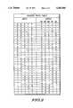
- FIG. 2illustrates in table form a truth table of a decoder in the tuning circuit of FIG. 1;
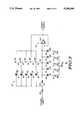
- FIG. 3illustrates in partial schematic form an analog filter for use with the tuning circuit of FIG. 1.
- a tuning circuit 10generally having an integrator with an input portion 12 and a comparator portion 14, a count portion 16, and a decode portion 18.
- a resistor 24has a first terminal connected to a first reference voltage, labeled "V REF 1 ".
- a second terminal of resistor 24is connected to an inverting or negative input of an operational amplifier 21.
- a noninverting or positive input of operational amplifier 21is connected to a second reference voltage labeled "V REF 2.”
- a capacitor 26has a first electrode connected to the negative input of operational amplifier 21.
- a second electrode of capacitor 26is connected to an output of operational amplifier 21.
- a switch 28has a first terminal connected to the first electrode of capacitor 26 and a second terminal connected to the output of operational amplifier 21.
- Switch 28has a control terminal for receiving a control signal labeled " ⁇ 1".
- Comparator portion 14has an operational amplifier 30 having an inverting or negative input connected to the output of operational amplifier 21.
- a noninverting or positive input of operational amplifier 30is connected to a third reference voltage labeled "V REF 3."
- V REF 3may have a voltage value which is either greater than or less than V REF 2.
- Each of the three reference voltagesare referenced with respect to some predetermined voltage, preferably a supply voltage V SS .
- An output of operational amplifier 30is connected to an enable input of a counter 32 of the count portion 16.
- Control signal ⁇ 1is connected to a Reset input of counter 32, and a system clock signal labeled "CLOCK” is connected to a clock input of counter 32.
- Counter 32provides a multi-bit count output. In the illustrated form, each of a plurality of five single-bit outputs is connected to one of a plurality of five inputs of a decoder 34 of decode portion 18. Decoder 34 provides five outputs respectively labeled "B0", “B1", “B2”, “B3”, and "B4".
- tuning circuit 10functions to provide a decoded output signal for use by an analog filter in adjusting the resistive/capacitive time constant of the filter to an optimum value. Because analog filters are made with analog components which vary in value over processing and temperature variations, adjustment of the analog components is desirable.
- Input portion 12 and comparator portion 14function to provide an enable signal to counter 32 for a predetermined amount of time. However, this predetermined amount of time will vary primarily as the values of capacitor 26 and resistor 24 vary with respect to processing and temperature.
- Input portion 12functions to integrate a fixed input current signal conducted at the negative input of operational amplifier 21. The time to perform this integration is proportional to the amount of time required to change capacitor 26 to substantially the V REF 2 voltage. Accordingly, switch 28 functions to periodically discharge capacitor 26 or autozero the operational amplifier 21.
- a ramp time, T ramp, of the integratormay be represented in equation one below as:
- Comparator portion 14functions to compare the output of input portion 12 with the value of V REF 3. Until the output of input portion 12 is greater than V REF 3 in value, counter 32 remains enabled. Once the output of input portion 12 equals V REF 3, counter 32 is disabled. During the time period which counter 32 is enabled, counter 32 is counting the number of clock cycles of the system CLOCK signal. The number of clock cycles which are counted while input portion 12 is integrating is provided by counter 32 as an output.
- the output of counter 32may be represented in equation two below as:
- T clockis the clock frequency period of the CLOCK signal connected to counter 32.
- the output of counter 32is decoded into a binary output value represented by bits B0 thru B4.
- Bits B0 thru B4are an encoded time constant variation compensation code of the RC time constant of input portion 12.
- FIG. 2Illustrated in FIG. 2 is a truth table for decoder 34.
- five input bits and five output bitsare discussed. It should be readily apparent that any number of decoder inputs/outputs may be utilized depending upon the amount of tuning resolution desired for the analog filtering.
- For a five-bit inputthere are 2 5 or thirty-two possible binary values.
- For each five-bit binary valuethere is an assigned predetermined binary output. As may be readily noted in FIG. 2, some of the binary inputs are assigned to the same binary output value for controlling the analog filter. Before an analysis of the assignment of output values for bits B0-B4 is made, a discussion of the effect which control bits B0-B4 have on an analog filter is desirable.
- Analog filter 40generally has a resistive/capacitive portion 42 and an amplifier portion 44. Within resistive/capacitive portion 42 there is provided an input terminal labeled "Filter input" for receiving a filter input. The input terminal is connected to a first terminal of a resistor 50. A second terminal of resistor 50 is connected at a node 51 to a first terminal of a resistor 52. A second terminal of resistor 52 is connected at a node 53 to a positive or noninverting input of an operational amplifier 54. Connected to node 53 is a first electrode of each of a plurality of binary weighted capacitors 60-64.
- capacitor 60has a designated unit weight of "C”
- capacitor 61has a designated weight of 2C
- capacitor 62has a designated weight of "4C”
- Each of capacitors 60-64has a second electrode connected to a first terminal of a respective one of a plurality of switches 70-74.
- the second electrode of capacitor 60is connected to the first terminal of switch 70, and so forth for capacitors 61-64 and switches 71-74.
- Each of switches 70-74has a second terminal connected to a reference voltage terminal for receiving a supply voltage labeled "V SS ".
- Each of switches 70-74has a control terminal for receiving a respective one of a plurality of control signals B0-B4 from the output of decoder 34 of FIG. 1.
- the control terminal of switch 70is connected to control signal B0
- the control terminal of switch 71is connected to control signal B1, and so forth.
- a first electrode of each of a plurality of binarily weighted capacitors 80-84is connected to node 51.
- capacitor 80has a designated unit weight of "C”
- capacitor 81has a designated weight of "2C”
- capacitor 82has a designated weight of "4C”
- Each of capacitors 80-84has a second electrode connected to a first terminal of a respective one of a plurality of switches 90-94.
- the second electrode capacitor 80is connected to the first terminal of switch 90, and so forth for capacitors 81-84 and switches 91-94.
- Each of switches 90-94has a second terminal connected to an inverting or negative input of operational amplifier 54.
- Each of switches 90-94has a control terminal for respectively receiving control signals B0-B4 from decoder 34 of FIG. 1.
- An output of operational amplifier 54is connected to the negative input thereof and to the second terminals of switches 90-94.
- the output of operational amplifier 54provides an output of analog filter 40 labeled "Filter Output.”
- an analog filter input signalis coupled to filter 40 at the filter input and filtered by operational amplifier 54 in combination with the net capacitive effect of capacitors 60-64 and 80-84 and resistors 50, 52.
- Resistors 50, 52 and capacitors 60-64 and 80-84function as a resistive/capacitive (RC) network having an effective RC time constant.
- the RC time constantestablishes a frequency pole of filter 40.
- Each of the resistors 50, 52 and capacitors 60-64, 80-84is subject to processing and temperature variation which can vary the frequency pole of filter 40 and otherwise vary the frequency response of the filter.
- the present inventionfunctions to use tuner circuit 10 to vary the capacitance of resistance/capacitance portion 42 to compensate for variations in both the resistance and capacitance of resistance/capacitance portion 42.
- the output of tuner 10may be readily modified to also directly control only resistive values in analog filter 40 or a combination of both resistive and capacitive values.
- variations in resistors 50, 52 and capacitors 60-64 and 80-84will generally directly track with variations in resistor 24 and capacitor 26 provided all of the resistors are fabricated to be of the same type and physical orientation (i.e. circuit layout) and all of the capacitors are fabricated to be of the same type and physical orientation.
- decoder 34can provide a dynamic signal which will control the amount of effective capacitance in the resistance/capacitance portion 42. Therefore, an effective method exists to maintain a constant frequency pole for analog filter 40 by selecting a variable number of capacitors in a bank of capacitors.
- the output valuecan assume a B0-B4 signal value which has the effect of switching in all of capacitors 60-64 and capacitors 80-84 in resistance/capacitance portion 42.
- the B0-B4 signal valuemay have the effect of switching only capacitors 60, 61 and 80-81 in resistance/capacitance portion 42.
- there is no B0-B4 output signalwhich has the effect of switching from only capacitor 60 to capacitor 61 and from capacitor 80 to capacitor 81. The reason to avoid switching from one unit of capacitance (i.e. capacitor 60) to two units of capacitance (i.e.
- capacitor 61is to avoid a two-to-one or one hundred percent change which creates very poor tuning resolution. It should be noted that the lowest valued output signal provided by decoder 34 is equivalent to three units of capacitance. The next highest increment is to increase to four units of capacitance which is an increase having a less negative effect on resolution.
- a predetermined input valueis chosen as being the value which represents the desired value of capacitance assuming that no error in the component values exists. The predetermined input value representing the desired value of capacitance should not preferably be in the middle of the input values. The predetermined input value representing the desired value of capacitance should be in the upper third of the range, i.e. in the lower value range of the inputs in order to permit better resolution at the low end of the capacitive switching range.
- the switching of capacitors having capacitive units between fifteen, sixteen, seventeen, eighteen, nineteen, twenty, etc. units of capacitanceis a much smaller change in percentage than when changing between one, three, four, etc., units of capacitance.
- the truth table of FIG. 2represents an efficient decoding which permits a deviation in the count value of counter 32 to be corrected with optimum resolution when using a five-bit count signal.
- the present inventionprovides a circuit which: (1) receives an analog input signal; (2) integrates the input signal with input portion 12; and (3) provides a digital equivalent of the analog input signal with count portion 16.
- the integrationis related to a predetermined RC time constant, where the resistance may also be implemented as a transconductance rather than a resistance.
- the known RC time constantis utilized to adjust another RC time constant having the same physical and electrical properties of another circuit.
- the digital equivalentmay be directly used if only a digital equivalent of the analog input signal is desired. In other forms, other decodings of the resulting digital equivalent of the analog input signal may be implemented.
- the tuning circuit and method taught hereinrequire no trimming or adjusting of component values. Also, no components which are external to an integrated circuit containing the filter are required.
- the tuner circuit taught hereindoes not rely on feedback and is therefore more stable than a phase lock loop.
- the decoder 34may be implemented as a programmable logic device (PLA), by conventional logic circuitry, or by a memory, as well as in other known forms. Similarly, many known counter circuits may be utilized as counter 32 of the inventive tuner. Although capacitors having a binary weighting have been discussed, it should be readily apparent that capacitors having other weighting factors (i.e.nary or logarithmic) may be used. Although a specific decoding has been provided for decoder 34, it should be noted that other decodings which implement a nonlinear relationship between the input and the output of decoder 34 may be used.
- an integratoris illustrated in the disclosed tuning circuit, other circuits which do not integrate but which have an RC time constant may be used.
- a filter stage having an RC networkmay be used rather than an integrator.
- the output of the filter stageis exponential rather than linear when an integrator is used.
- An implementation with an integratoris generally preferable because the linear output of the integrator ensures that the response time of comparator portion 14 will not be variable. If an exponential signal is input into comparator portion 14, the response time of the comparator will be variable.
Landscapes
- Networks Using Active Elements (AREA)
Abstract
Description
T ramp=[(V.sub.REF 3 -V.sub.REF 2)/(V.sub.REF 2 -V.sub.REF 1)]* R.sub.24 * C.sub.26 (1)
Output ofCounter 32=[T ramp]/[T clock] (2)
Claims (11)
Priority Applications (1)
| Application Number | Priority Date | Filing Date | Title |
|---|---|---|---|
| US07/891,082US5245646A (en) | 1992-06-01 | 1992-06-01 | Tuning circuit for use with an integrated continuous time analog filter |
Applications Claiming Priority (1)
| Application Number | Priority Date | Filing Date | Title |
|---|---|---|---|
| US07/891,082US5245646A (en) | 1992-06-01 | 1992-06-01 | Tuning circuit for use with an integrated continuous time analog filter |
Publications (1)
| Publication Number | Publication Date |
|---|---|
| US5245646Atrue US5245646A (en) | 1993-09-14 |
Family
ID=25397583
Family Applications (1)
| Application Number | Title | Priority Date | Filing Date |
|---|---|---|---|
| US07/891,082Expired - LifetimeUS5245646A (en) | 1992-06-01 | 1992-06-01 | Tuning circuit for use with an integrated continuous time analog filter |
Country Status (1)
| Country | Link |
|---|---|
| US (1) | US5245646A (en) |
Cited By (39)
| Publication number | Priority date | Publication date | Assignee | Title |
|---|---|---|---|---|
| US5416438A (en)* | 1992-03-18 | 1995-05-16 | Nec Corporation | Active filter circuit suited to integration on IC chip |
| US5473278A (en)* | 1993-02-15 | 1995-12-05 | Nec Corporation | Filter circuit including a switch circuit inserted between input terminal and RC filter |
| EP0851378A1 (en)* | 1996-12-30 | 1998-07-01 | Datalogic S.P.A. | Method and device for measuring and regulating a time constant of an electronic circuit forming part of an optical code reader |
| US5883545A (en)* | 1998-01-14 | 1999-03-16 | Pmc-Sierra Ltd. | Training method for GM-C or MOS-C Circuits |
| US5914633A (en)* | 1997-08-08 | 1999-06-22 | Lucent Technologies Inc. | Method and apparatus for tuning a continuous time filter |
| US5966047A (en)* | 1997-03-27 | 1999-10-12 | Motorola, Inc. | Programmable analog array and method |
| US5966054A (en)* | 1998-01-29 | 1999-10-12 | Motorola, Inc. | Method and apparatus for providing a clocking signal |
| US5994951A (en)* | 1997-01-21 | 1999-11-30 | Vtc Inc. | Automatic-tuning circuit for integrated continuous-time MOSFET-C filters |
| US6356142B1 (en)* | 2000-09-20 | 2002-03-12 | Motorola, Inc. | Digital filter tune loop |
| US6452444B1 (en) | 2001-02-13 | 2002-09-17 | Analog Devices, Inc. | Method and apparatus for background calibration of active RC filters |
| WO2002073801A1 (en)* | 2001-03-09 | 2002-09-19 | National Semiconductor Corporation | Filter trimming |
| US6509792B2 (en)* | 2000-06-27 | 2003-01-21 | Infineon Technologies Ag | Circuit and method for attenuating or eliminating undesired properties of an operational amplifier |
| US20030086516A1 (en)* | 2000-05-08 | 2003-05-08 | Elmar Wagner | Compensation circuit and method for compensating for an offset |
| WO2003063352A1 (en)* | 2002-01-17 | 2003-07-31 | Microtune (San Diego), Inc. | Method and apparatus for filter tuning |
| US6628163B2 (en)* | 2001-11-15 | 2003-09-30 | Advanced Micro Devices, Inc. | Circuit for tuning an active filter |
| WO2003005583A3 (en)* | 2001-06-29 | 2003-11-06 | Koninkl Philips Electronics Nv | A reconfigurable analog cell and an arrangement comprising a plurality of such cell |
| US20040124911A1 (en)* | 2001-05-03 | 2004-07-01 | Christian Fleischhacker | Method and apparatus for adjusting an active filter |
| US20050024252A1 (en)* | 2003-07-28 | 2005-02-03 | Microtune (Texas), L.P. | Method and system for filter tuning using a digital trim value |
| US20050040831A1 (en)* | 2003-08-21 | 2005-02-24 | Ibrahim Brima B. | Filter calibration and applications thereof |
| US20050046487A1 (en)* | 2003-08-27 | 2005-03-03 | Nokia Corporation | Calibrating a loop-filter of a phase locked loop |
| US6891436B2 (en) | 2002-09-30 | 2005-05-10 | Integrant Technologies Inc. | Transconductance varying circuit of transconductor circuit, varying bandwidth filter circuit using the same and digital tuning circuit of transconductor-capacitor filter |
| US6937089B2 (en)* | 2003-12-30 | 2005-08-30 | Freescale Semiconductor, Inc. | Offset, delay and parasitically immune resister-capacitor (RC) tracking loop and method of using same |
| US7002404B2 (en)* | 2003-02-27 | 2006-02-21 | Infineon Technologies Ag | Tuning circuit for a filter |
| US7019586B2 (en)* | 2004-03-23 | 2006-03-28 | Silicon Laboratories Inc. | High-speed Gm-C tuning |
| US20070109063A1 (en)* | 2005-11-14 | 2007-05-17 | Wai Lau | On-chip R-C time constant calibration |
| US7313201B2 (en) | 2003-07-28 | 2007-12-25 | Microtune (Texas), L.P. | Multi-range transconductor and method of operation |
| US20080096514A1 (en)* | 2006-10-18 | 2008-04-24 | Freescale Semiconductor, Inc. | Controlling the bandwidth of an analog filter |
| US20080180300A1 (en)* | 2007-01-31 | 2008-07-31 | Hynix Semiconductor Inc. | Analog-digital converter and on-die thermal sensor including the same |
| US20080191794A1 (en)* | 2007-02-08 | 2008-08-14 | Mediatek Inc. | Method and apparatus for tuning an active filter |
| US20080191795A1 (en)* | 2007-02-08 | 2008-08-14 | Mediatek Singapore Pte Ltd | Method and apparatus for tuning an active filter |
| US20090108858A1 (en)* | 2007-10-24 | 2009-04-30 | Industrial Technology Research Institute | Methods and systems for calibrating rc circuits |
| US20100013546A1 (en)* | 2006-12-01 | 2010-01-21 | Jung-Hoon Yoo | Systems and methods for filter tuning using binary search algorithm |
| US20100073048A1 (en)* | 2008-09-24 | 2010-03-25 | Mediatek Inc. | Phase locked loop and calibration method |
| US20100323651A1 (en)* | 2009-06-23 | 2010-12-23 | Qualcomm Incorporated | Tunable adaptive filter with variable gain trans-conductance stage |
| US20110128071A1 (en)* | 2009-11-27 | 2011-06-02 | Masaru Fukusen | Filter automatic adjustment circuit and method for adjusting characteristic frequency of filter, and wireless communication apparatus provided with the same |
| US20110169591A1 (en)* | 2010-01-08 | 2011-07-14 | Fci Inc. | Filter cut-off frequency correction circuit |
| US20110221503A1 (en)* | 2010-03-09 | 2011-09-15 | Renesas Electronics Corporation | Semiconductor integrated circuit including constant adjusting circuit |
| US9030213B2 (en) | 2009-01-28 | 2015-05-12 | St-Ericsson Sa | Method and system for measuring a time constant of an integrated circuit, and integrated circuit provided with such a system |
| US10367478B2 (en)* | 2016-04-01 | 2019-07-30 | Shenzhen GOODIX Technology Co., Ltd. | Window function processing module |
Citations (14)
| Publication number | Priority date | Publication date | Assignee | Title |
|---|---|---|---|---|
| US3818246A (en)* | 1971-04-06 | 1974-06-18 | Ibm | Switching circuits particularly useful for analog-to-digital converters |
| US4352010A (en)* | 1980-02-13 | 1982-09-28 | R. L. Drake Company | Variable rate tuning for radio transmitters and receivers |
| US4661803A (en)* | 1985-04-27 | 1987-04-28 | Tokyo Electric Co., Ltd. | Analog/digital converter |
| US4672361A (en)* | 1984-09-07 | 1987-06-09 | Hitachi, Ltd. | Linear interpolative analog-to-digital converter |
| US4675649A (en)* | 1985-09-11 | 1987-06-23 | Halliburton Company | Apparatus and method for interfacing a transducer |
| US4733205A (en)* | 1986-04-30 | 1988-03-22 | U.S. Philips Corporation | Electrical filter |
| US4783644A (en)* | 1985-04-11 | 1988-11-08 | Amdahl Corporation | Continuously variable slope delta modulation using digital vector for slope control |
| US4791379A (en)* | 1985-02-13 | 1988-12-13 | U.S. Philips Corporation | Electrical filter with adjustable RC product |
| US4939519A (en)* | 1986-02-03 | 1990-07-03 | Thaler Corporation | Apparatus for method and a high precision analog-to-digital converter |
| US4965578A (en)* | 1987-10-21 | 1990-10-23 | Commissariat A L'energie Atomique | High dynamic analog to digital counter |
| US5059836A (en)* | 1988-12-09 | 1991-10-22 | Dallas Semiconductor Corporation | Differential-time-constant bandpass filter using the analog properties of digital circuits |
| US5124593A (en)* | 1990-09-26 | 1992-06-23 | National Semiconductor Corporation | Continuous-time filter tuning circuit and method |
| US5128676A (en)* | 1990-06-05 | 1992-07-07 | Blh Electronics, Inc. | Variable conversion rate analog-to-digital converter |
| US5187445A (en)* | 1991-10-28 | 1993-02-16 | Motorola, Inc. | Tuning circuit for continuous-time filters and method therefor |
- 1992
- 1992-06-01USUS07/891,082patent/US5245646A/ennot_activeExpired - Lifetime
Patent Citations (14)
| Publication number | Priority date | Publication date | Assignee | Title |
|---|---|---|---|---|
| US3818246A (en)* | 1971-04-06 | 1974-06-18 | Ibm | Switching circuits particularly useful for analog-to-digital converters |
| US4352010A (en)* | 1980-02-13 | 1982-09-28 | R. L. Drake Company | Variable rate tuning for radio transmitters and receivers |
| US4672361A (en)* | 1984-09-07 | 1987-06-09 | Hitachi, Ltd. | Linear interpolative analog-to-digital converter |
| US4791379A (en)* | 1985-02-13 | 1988-12-13 | U.S. Philips Corporation | Electrical filter with adjustable RC product |
| US4783644A (en)* | 1985-04-11 | 1988-11-08 | Amdahl Corporation | Continuously variable slope delta modulation using digital vector for slope control |
| US4661803A (en)* | 1985-04-27 | 1987-04-28 | Tokyo Electric Co., Ltd. | Analog/digital converter |
| US4675649A (en)* | 1985-09-11 | 1987-06-23 | Halliburton Company | Apparatus and method for interfacing a transducer |
| US4939519A (en)* | 1986-02-03 | 1990-07-03 | Thaler Corporation | Apparatus for method and a high precision analog-to-digital converter |
| US4733205A (en)* | 1986-04-30 | 1988-03-22 | U.S. Philips Corporation | Electrical filter |
| US4965578A (en)* | 1987-10-21 | 1990-10-23 | Commissariat A L'energie Atomique | High dynamic analog to digital counter |
| US5059836A (en)* | 1988-12-09 | 1991-10-22 | Dallas Semiconductor Corporation | Differential-time-constant bandpass filter using the analog properties of digital circuits |
| US5128676A (en)* | 1990-06-05 | 1992-07-07 | Blh Electronics, Inc. | Variable conversion rate analog-to-digital converter |
| US5124593A (en)* | 1990-09-26 | 1992-06-23 | National Semiconductor Corporation | Continuous-time filter tuning circuit and method |
| US5187445A (en)* | 1991-10-28 | 1993-02-16 | Motorola, Inc. | Tuning circuit for continuous-time filters and method therefor |
Non-Patent Citations (2)
| Title |
|---|
| IEEE Transactions On Circuits and Systems, vol. 33, No. 2, Feb. 1986, New York, U.S., Tsividis, "Continuous-Time MOSFET-C Filters In VLSI", pp. 125-140. |
| IEEE Transactions On Circuits and Systems, vol. 33, No. 2, Feb. 1986, New York, U.S., Tsividis, Continuous Time MOSFET C Filters In VLSI , pp. 125 140.* |
Cited By (67)
| Publication number | Priority date | Publication date | Assignee | Title |
|---|---|---|---|---|
| US5416438A (en)* | 1992-03-18 | 1995-05-16 | Nec Corporation | Active filter circuit suited to integration on IC chip |
| US5473278A (en)* | 1993-02-15 | 1995-12-05 | Nec Corporation | Filter circuit including a switch circuit inserted between input terminal and RC filter |
| EP0851378A1 (en)* | 1996-12-30 | 1998-07-01 | Datalogic S.P.A. | Method and device for measuring and regulating a time constant of an electronic circuit forming part of an optical code reader |
| US5994951A (en)* | 1997-01-21 | 1999-11-30 | Vtc Inc. | Automatic-tuning circuit for integrated continuous-time MOSFET-C filters |
| US5966047A (en)* | 1997-03-27 | 1999-10-12 | Motorola, Inc. | Programmable analog array and method |
| US5914633A (en)* | 1997-08-08 | 1999-06-22 | Lucent Technologies Inc. | Method and apparatus for tuning a continuous time filter |
| US5883545A (en)* | 1998-01-14 | 1999-03-16 | Pmc-Sierra Ltd. | Training method for GM-C or MOS-C Circuits |
| US5966054A (en)* | 1998-01-29 | 1999-10-12 | Motorola, Inc. | Method and apparatus for providing a clocking signal |
| US20030086516A1 (en)* | 2000-05-08 | 2003-05-08 | Elmar Wagner | Compensation circuit and method for compensating for an offset |
| US6823024B2 (en)* | 2000-05-08 | 2004-11-23 | Infineon Technologies Ag | Compensation circuit and method for compensating for an offset |
| US6509792B2 (en)* | 2000-06-27 | 2003-01-21 | Infineon Technologies Ag | Circuit and method for attenuating or eliminating undesired properties of an operational amplifier |
| US6356142B1 (en)* | 2000-09-20 | 2002-03-12 | Motorola, Inc. | Digital filter tune loop |
| US6452444B1 (en) | 2001-02-13 | 2002-09-17 | Analog Devices, Inc. | Method and apparatus for background calibration of active RC filters |
| US6686809B2 (en)* | 2001-03-09 | 2004-02-03 | National Semiconductor Corporation | Filter trimming |
| WO2002073801A1 (en)* | 2001-03-09 | 2002-09-19 | National Semiconductor Corporation | Filter trimming |
| US7002427B2 (en) | 2001-03-09 | 2006-02-21 | National Semiconductor Corporation | Filter trimming |
| US20040212447A1 (en)* | 2001-03-09 | 2004-10-28 | Christian Nystrom | Filter trimming |
| US20040124911A1 (en)* | 2001-05-03 | 2004-07-01 | Christian Fleischhacker | Method and apparatus for adjusting an active filter |
| US7116159B2 (en)* | 2001-05-03 | 2006-10-03 | Infineon Technologies Ag | Method and apparatus for adjusting an active filter |
| WO2003005583A3 (en)* | 2001-06-29 | 2003-11-06 | Koninkl Philips Electronics Nv | A reconfigurable analog cell and an arrangement comprising a plurality of such cell |
| US6628163B2 (en)* | 2001-11-15 | 2003-09-30 | Advanced Micro Devices, Inc. | Circuit for tuning an active filter |
| DE10156027B4 (en)* | 2001-11-15 | 2012-02-09 | Globalfoundries Inc. | Adjustable filter circuit |
| US6677814B2 (en)* | 2002-01-17 | 2004-01-13 | Microtune (San Diego), Inc. | Method and apparatus for filter tuning |
| WO2003063352A1 (en)* | 2002-01-17 | 2003-07-31 | Microtune (San Diego), Inc. | Method and apparatus for filter tuning |
| US6958652B2 (en) | 2002-09-30 | 2005-10-25 | Integrant Technologies Inc. | Transconductance varying circuit of transconductor circuit, varying bandwidth filter circuit using the same and digital tuning circuit of transconductor-capacitor filter |
| US6891436B2 (en) | 2002-09-30 | 2005-05-10 | Integrant Technologies Inc. | Transconductance varying circuit of transconductor circuit, varying bandwidth filter circuit using the same and digital tuning circuit of transconductor-capacitor filter |
| US20050162194A1 (en)* | 2002-09-30 | 2005-07-28 | Integrant Technologies Inc. | Transconductance varying circuit of transconductor circuit, varying bandwidth filter circuit using the same and digital tuning circuit of transconductor-capacitor filter |
| US7002404B2 (en)* | 2003-02-27 | 2006-02-21 | Infineon Technologies Ag | Tuning circuit for a filter |
| US7078960B2 (en) | 2003-07-28 | 2006-07-18 | Microtune (Texas), L.P. | Method and system for filter tuning using a digital trim value |
| WO2005013483A3 (en)* | 2003-07-28 | 2005-04-28 | Microtune Texas Lp | Method and system for filter tuning using a digital trim value |
| US20050024252A1 (en)* | 2003-07-28 | 2005-02-03 | Microtune (Texas), L.P. | Method and system for filter tuning using a digital trim value |
| US7313201B2 (en) | 2003-07-28 | 2007-12-25 | Microtune (Texas), L.P. | Multi-range transconductor and method of operation |
| US6914437B2 (en)* | 2003-08-21 | 2005-07-05 | Broadcom Corp. | Filter calibration and applications thereof |
| US20050189951A1 (en)* | 2003-08-21 | 2005-09-01 | Ibrahim Brima B. | Filter calibration |
| US7345490B2 (en)* | 2003-08-21 | 2008-03-18 | Broadcom Corporation | Filter calibration |
| US20050040831A1 (en)* | 2003-08-21 | 2005-02-24 | Ibrahim Brima B. | Filter calibration and applications thereof |
| WO2005022753A1 (en)* | 2003-08-27 | 2005-03-10 | Nokia Corporation | Calibrating a loop-filter of a phase locked loop |
| CN1813407B (en)* | 2003-08-27 | 2011-10-26 | 诺基亚公司 | Method and device for automatically calibrating a loop-filter of a phase locked loop |
| KR100831651B1 (en)* | 2003-08-27 | 2008-05-22 | 노키아 코포레이션 | Calibrating a loop-filter of a phase locked loop |
| US20050046487A1 (en)* | 2003-08-27 | 2005-03-03 | Nokia Corporation | Calibrating a loop-filter of a phase locked loop |
| US6972633B2 (en) | 2003-08-27 | 2005-12-06 | Nokia Corporation | Calibrating a loop-filter of a phase locked loop |
| US6937089B2 (en)* | 2003-12-30 | 2005-08-30 | Freescale Semiconductor, Inc. | Offset, delay and parasitically immune resister-capacitor (RC) tracking loop and method of using same |
| US7019586B2 (en)* | 2004-03-23 | 2006-03-28 | Silicon Laboratories Inc. | High-speed Gm-C tuning |
| US20070109063A1 (en)* | 2005-11-14 | 2007-05-17 | Wai Lau | On-chip R-C time constant calibration |
| US7548129B2 (en) | 2005-11-14 | 2009-06-16 | Quantek, Inc. | On-chip R-C time constant calibration |
| US20080096514A1 (en)* | 2006-10-18 | 2008-04-24 | Freescale Semiconductor, Inc. | Controlling the bandwidth of an analog filter |
| US7937058B2 (en) | 2006-10-18 | 2011-05-03 | Freescale Semiconductor, Inc. | Controlling the bandwidth of an analog filter |
| US7944286B2 (en)* | 2006-12-01 | 2011-05-17 | Xronet Corporation | Systems and methods for filter tuning using binary search algorithm |
| US20100013546A1 (en)* | 2006-12-01 | 2010-01-21 | Jung-Hoon Yoo | Systems and methods for filter tuning using binary search algorithm |
| US20080180300A1 (en)* | 2007-01-31 | 2008-07-31 | Hynix Semiconductor Inc. | Analog-digital converter and on-die thermal sensor including the same |
| US7880661B2 (en)* | 2007-01-31 | 2011-02-01 | Hynix Semiconductor Inc. | Analog-digital converter and on-die thermal sensor including the same |
| US20080191795A1 (en)* | 2007-02-08 | 2008-08-14 | Mediatek Singapore Pte Ltd | Method and apparatus for tuning an active filter |
| US7477098B2 (en) | 2007-02-08 | 2009-01-13 | Mediatek Singapore Pte Ltd | Method and apparatus for tuning an active filter |
| US20080191794A1 (en)* | 2007-02-08 | 2008-08-14 | Mediatek Inc. | Method and apparatus for tuning an active filter |
| US20090108858A1 (en)* | 2007-10-24 | 2009-04-30 | Industrial Technology Research Institute | Methods and systems for calibrating rc circuits |
| US20100073048A1 (en)* | 2008-09-24 | 2010-03-25 | Mediatek Inc. | Phase locked loop and calibration method |
| EP2382709B1 (en)* | 2009-01-28 | 2016-08-17 | ST-Ericsson SA | Method and system for measuring a time constant of an integrated circuit, and integrated circuit provided with such a system |
| US9030213B2 (en) | 2009-01-28 | 2015-05-12 | St-Ericsson Sa | Method and system for measuring a time constant of an integrated circuit, and integrated circuit provided with such a system |
| JP2012531819A (en)* | 2009-06-23 | 2012-12-10 | クゥアルコム・インコーポレイテッド | Adaptive filter tunable with variable gain transconductance stage |
| US20100323651A1 (en)* | 2009-06-23 | 2010-12-23 | Qualcomm Incorporated | Tunable adaptive filter with variable gain trans-conductance stage |
| US9602079B2 (en)* | 2009-06-23 | 2017-03-21 | Qualcomm Incorporated | Tunable adaptive filter with variable gain trans-conductance stage |
| KR20120030154A (en)* | 2009-06-23 | 2012-03-27 | 퀄컴 인코포레이티드 | Tunable adaptive filter with variable gain trans-conductance stage |
| US20110128071A1 (en)* | 2009-11-27 | 2011-06-02 | Masaru Fukusen | Filter automatic adjustment circuit and method for adjusting characteristic frequency of filter, and wireless communication apparatus provided with the same |
| US8044710B2 (en)* | 2010-01-08 | 2011-10-25 | Fci Inc. | Filter cut-off frequency correction circuit |
| US20110169591A1 (en)* | 2010-01-08 | 2011-07-14 | Fci Inc. | Filter cut-off frequency correction circuit |
| US20110221503A1 (en)* | 2010-03-09 | 2011-09-15 | Renesas Electronics Corporation | Semiconductor integrated circuit including constant adjusting circuit |
| US10367478B2 (en)* | 2016-04-01 | 2019-07-30 | Shenzhen GOODIX Technology Co., Ltd. | Window function processing module |
Similar Documents
| Publication | Publication Date | Title |
|---|---|---|
| US5245646A (en) | Tuning circuit for use with an integrated continuous time analog filter | |
| US5187445A (en) | Tuning circuit for continuous-time filters and method therefor | |
| US5914633A (en) | Method and apparatus for tuning a continuous time filter | |
| US4764750A (en) | Analog-to-digital converter | |
| CN1120267A (en) | A tuning circuit | |
| US7626449B2 (en) | Apparatus and method for tuning center frequency of a filter | |
| US5621355A (en) | Sampled data-biasing of continuous time integrated circuit | |
| EP1755218B1 (en) | Tunable resonator for use in active-RC continuous-time filters | |
| US6097244A (en) | Highly-linear continuous-time filter for a 3-volt supply with PLL-controlled resistor and digitally-controlled capacitor | |
| US6646498B2 (en) | High frequency tunable filter | |
| US5543754A (en) | Capacitor and resistor controlled oscillator timing lock loop for precision time constants | |
| US4429285A (en) | Frequency-controlled variable-gain amplifiers | |
| US4595910A (en) | Digital-to-analog converter useful in a television receiver | |
| CN113098522A (en) | Multiplying digital-to-analog converter with increased multiplication bandwidth | |
| US4462021A (en) | Digital-to-analog converter that compensates for integrated circuit resistor variations | |
| US7098730B1 (en) | Process variation trim/tuning for continuous time filters and Δ-Σ analog to digital converters | |
| CA2603897C (en) | Network with muliple adjustment elements and sensitivities, and digital-to-analog converter implementing same | |
| JP4723215B2 (en) | Filter circuit that enables adjustment of cut-off frequency | |
| US6919759B2 (en) | Digitally controlled tuner circuit | |
| US4352206A (en) | Comparison arrangement for a digital tuning system | |
| US5243548A (en) | Integratable circuit configuration with an analog network | |
| GB2073981A (en) | Frequency comparison arrangement for a digital tuning system | |
| KR100252961B1 (en) | frequency compensating circuit | |
| Xia et al. | An auto-tuning structure for continuous time sigma-delta AD converter and high precision filters | |
| Pun et al. | Current-division-based digital frequency tuning for active RC filters |
Legal Events
| Date | Code | Title | Description |
|---|---|---|---|
| AS | Assignment | Owner name:MOTOROLA, INC. A CORP. OF DELAWARE, ILLINOIS Free format text:ASSIGNMENT OF ASSIGNORS INTEREST.;ASSIGNORS:JACKSON, H. SPENCE;WHATLEY, ROGER A.;REEL/FRAME:006141/0629 Effective date:19920527 | |
| STCF | Information on status: patent grant | Free format text:PATENTED CASE | |
| FPAY | Fee payment | Year of fee payment:4 | |
| FPAY | Fee payment | Year of fee payment:8 | |
| AS | Assignment | Owner name:FREESCALE SEMICONDUCTOR, INC., TEXAS Free format text:ASSIGNMENT OF ASSIGNORS INTEREST;ASSIGNOR:MOTOROLA, INC.;REEL/FRAME:015698/0657 Effective date:20040404 Owner name:FREESCALE SEMICONDUCTOR, INC.,TEXAS Free format text:ASSIGNMENT OF ASSIGNORS INTEREST;ASSIGNOR:MOTOROLA, INC.;REEL/FRAME:015698/0657 Effective date:20040404 | |
| FPAY | Fee payment | Year of fee payment:12 | |
| AS | Assignment | Owner name:CITIBANK, N.A. AS COLLATERAL AGENT, NEW YORK Free format text:SECURITY AGREEMENT;ASSIGNORS:FREESCALE SEMICONDUCTOR, INC.;FREESCALE ACQUISITION CORPORATION;FREESCALE ACQUISITION HOLDINGS CORP.;AND OTHERS;REEL/FRAME:018855/0129 Effective date:20061201 Owner name:CITIBANK, N.A. AS COLLATERAL AGENT,NEW YORK Free format text:SECURITY AGREEMENT;ASSIGNORS:FREESCALE SEMICONDUCTOR, INC.;FREESCALE ACQUISITION CORPORATION;FREESCALE ACQUISITION HOLDINGS CORP.;AND OTHERS;REEL/FRAME:018855/0129 Effective date:20061201 | |
| AS | Assignment | Owner name:CITIBANK, N.A., AS COLLATERAL AGENT,NEW YORK Free format text:SECURITY AGREEMENT;ASSIGNOR:FREESCALE SEMICONDUCTOR, INC.;REEL/FRAME:024397/0001 Effective date:20100413 Owner name:CITIBANK, N.A., AS COLLATERAL AGENT, NEW YORK Free format text:SECURITY AGREEMENT;ASSIGNOR:FREESCALE SEMICONDUCTOR, INC.;REEL/FRAME:024397/0001 Effective date:20100413 | |
| AS | Assignment | Owner name:FREESCALE SEMICONDUCTOR, INC., TEXAS Free format text:PATENT RELEASE;ASSIGNOR:CITIBANK, N.A., AS COLLATERAL AGENT;REEL/FRAME:037356/0143 Effective date:20151207 Owner name:FREESCALE SEMICONDUCTOR, INC., TEXAS Free format text:PATENT RELEASE;ASSIGNOR:CITIBANK, N.A., AS COLLATERAL AGENT;REEL/FRAME:037356/0553 Effective date:20151207 Owner name:FREESCALE SEMICONDUCTOR, INC., TEXAS Free format text:PATENT RELEASE;ASSIGNOR:CITIBANK, N.A., AS COLLATERAL AGENT;REEL/FRAME:037354/0225 Effective date:20151207 |