US5244554A - Method of producing recording media and its apparatus - Google Patents
Method of producing recording media and its apparatusDownload PDFInfo
- Publication number
- US5244554A US5244554AUS07/716,927US71692791AUS5244554AUS 5244554 AUS5244554 AUS 5244554AUS 71692791 AUS71692791 AUS 71692791AUS 5244554 AUS5244554 AUS 5244554A
- Authority
- US
- United States
- Prior art keywords
- recording media
- chamber
- substrate carrier
- substrates
- plasma
- Prior art date
- Legal status (The legal status is an assumption and is not a legal conclusion. Google has not performed a legal analysis and makes no representation as to the accuracy of the status listed.)
- Expired - Lifetime
Links
Images


Classifications
- C—CHEMISTRY; METALLURGY
- C23—COATING METALLIC MATERIAL; COATING MATERIAL WITH METALLIC MATERIAL; CHEMICAL SURFACE TREATMENT; DIFFUSION TREATMENT OF METALLIC MATERIAL; COATING BY VACUUM EVAPORATION, BY SPUTTERING, BY ION IMPLANTATION OR BY CHEMICAL VAPOUR DEPOSITION, IN GENERAL; INHIBITING CORROSION OF METALLIC MATERIAL OR INCRUSTATION IN GENERAL
- C23C—COATING METALLIC MATERIAL; COATING MATERIAL WITH METALLIC MATERIAL; SURFACE TREATMENT OF METALLIC MATERIAL BY DIFFUSION INTO THE SURFACE, BY CHEMICAL CONVERSION OR SUBSTITUTION; COATING BY VACUUM EVAPORATION, BY SPUTTERING, BY ION IMPLANTATION OR BY CHEMICAL VAPOUR DEPOSITION, IN GENERAL
- C23C14/00—Coating by vacuum evaporation, by sputtering or by ion implantation of the coating forming material
- C23C14/22—Coating by vacuum evaporation, by sputtering or by ion implantation of the coating forming material characterised by the process of coating
- C23C14/56—Apparatus specially adapted for continuous coating; Arrangements for maintaining the vacuum, e.g. vacuum locks
- C23C14/564—Means for minimising impurities in the coating chamber such as dust, moisture, residual gases
- C—CHEMISTRY; METALLURGY
- C23—COATING METALLIC MATERIAL; COATING MATERIAL WITH METALLIC MATERIAL; CHEMICAL SURFACE TREATMENT; DIFFUSION TREATMENT OF METALLIC MATERIAL; COATING BY VACUUM EVAPORATION, BY SPUTTERING, BY ION IMPLANTATION OR BY CHEMICAL VAPOUR DEPOSITION, IN GENERAL; INHIBITING CORROSION OF METALLIC MATERIAL OR INCRUSTATION IN GENERAL
- C23C—COATING METALLIC MATERIAL; COATING MATERIAL WITH METALLIC MATERIAL; SURFACE TREATMENT OF METALLIC MATERIAL BY DIFFUSION INTO THE SURFACE, BY CHEMICAL CONVERSION OR SUBSTITUTION; COATING BY VACUUM EVAPORATION, BY SPUTTERING, BY ION IMPLANTATION OR BY CHEMICAL VAPOUR DEPOSITION, IN GENERAL
- C23C14/00—Coating by vacuum evaporation, by sputtering or by ion implantation of the coating forming material
- C23C14/22—Coating by vacuum evaporation, by sputtering or by ion implantation of the coating forming material characterised by the process of coating
- C23C14/56—Apparatus specially adapted for continuous coating; Arrangements for maintaining the vacuum, e.g. vacuum locks
- C23C14/568—Transferring the substrates through a series of coating stations
Definitions
- This inventionrelates to a method of producing recording media having high recording density and high coercivity and its apparatus.
- chromium sublayeris formed on a substrate for recording media (hereinafter substrate), and a magnetic layer is formed on the sublayer by sputtering magnetic alloy such as Co-Ni-Cr.
- substratea substrate for recording media
- sputtering magnetic alloysuch as Co-Ni-Cr.
- One sputtering methodis called the stationary opposing type in which a disk-like target and a substrate are disposed with those centers aligned, and one method is called The passing by type or in-line type in which a magnetic film is sputtered on the substrate while a carrier arranged with many substrates passes between the targets.
- the sputtered particles adhered to the carrier of substrates and the impurities adhered to the sputtered particlesare detrimental to magnetic properties, and in particular, to the coercivity of the magnetic recording media.
- the inventorsto achieve the purpose, have made an intensive study on a method of removing impurities adhered to the carrier arranged with substrates. As a result, the inventors found a magnetic recording media having high coercivity and excellent in recording property is obtained by arranging substrates on a carrier which is purified by etching with a plasma state gas. (hereinafter etching by a plasma state gas is called plasma etching).
- This inventionprovides the following:
- a method of producing recording mediain which substrates for recording media are arranged on the carrier which has been purified by etching with a plasma state gas, and sputtering layers onto the substrates.
- An apparatus for producing recording mediawhich is composed of at least a sputtering chamber for forming the recording media, and a treatment chamber for purifying the carrier for substrates, using a plasma state gas before the sputtering.
- An etching treatment devicehaving a treatment chamber for purifying the carrier using plasma state gas, having an intake hole and an exhaust hole, and electrodes which are electrically insulated from the walls of the treatment chamber, for applying an electric voltage between the walls and the carrier.
- FIG. 1is a sectional top view showing an embodiment of the device according to the invention.
- FIG. 2is a total view showing and embodiment of a carrier
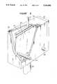
- FIG. 3is a perspective view showing an embodiment of an etching treatment device according the invention.
- FIG. 4is a longitudinal sectional view of an embodiment of an etching treatment device according to the present invention.
- a numeral 1designates a substrate removal chamber, 2, an etching chamber, 3, a substrate arranging chamber, 4, a heating chamber, 5, a sublayer and magnetic layer sputtering chamber, 6, a separation chamber, 7, a protection layer sputtering chamber, 8, a removal chamber, 9 to 16, gates, 17, a target for sputtering sublayer, 18, a target for sputtering magnetic layer, 19, a target for sputtering protection layer, 20 to 25, cryopumps, 26, a heater, 27, a differential exhaust device, 28, a carrier, 29, substrate arranging portion, 30, a treatment chamber, 31, a gas intake pipe, 32, a gas distribution pipe, 33, a gas exhaust pipe, 34, an electrode for carrier, 35, a gate, 36, an opposing electrode, 37, a carrier conveyor, 38, a rail for carrier conveyor, 39, a driving device for carrier conveyor, 40, a ceramic insulation material.
- the carrier of the substratesutilizes, as its material, aluminum, aluminum alloy, stainless steel, ceramic such as alumina, and heat resistant resin such as polyimide.
- the unit of degassing quantityis ⁇ 10 -5 torr ⁇ l/sec.
- Cosignifies an alloy having an atomic percentage of CoNi 30 Cr 7 .5.
- Cr+Co+C+Cr+Cosignifies that Co, C, Cr, and Co are successively formed on Cr.
- the degassing quantity of the filmmay reach about three times as large as that in the case wherein the sample has only chromium sublayer and cobalt alloy layer.
- the gascontains more than 80% of water. Accordingly, it is found that by removing the impurity particles, above all, carbon adhered by sputtering, by a plasma etching, the adhesion of water molecule is prevented, and the undesirable influence on the magnetic property can be extinguished.
- a magnetic recording mediais produced by forming a chromium sublayer, a magnetic layer and a carbon protective layer on substrates for magnetic recording media by sputtering, components constituting the respective layers are adhered to the carrier arranged with the substrates, and impurities such as H 2 O are also adhered to them.
- impuritiessuch as H 2 O are also adhered to them.
- This inventionis a method of producing recording media and its apparatus in which sputtered layers are formed on a substrate by arranging the substrate on a carrier which is purified by etching with a plasma state gas, by which recording media having excellent recording property is produced.
- argonAs a gas for the plasma etching, argon, nitrogen, and oxygen, and the mixtures of these gases are desirable. However gasses such as CF 4 and CCl 2 can be utilized.
- the pressure of the plasma etching gasis disirable to be in the range of 10 -3 to 10 -2 . However in case of argon, the pressure range of 0.01 to 0.1 torr is desirable, in case of argon+oxygen, 0.05 to 0.5 torr, and in case of oxygen, 0.1 to 5 torr. Compared with inert gas such as argon, in case of a reactive gas, the higher the pressure the better.
- the power source generating the plasma state gas to perform the plasma etchingmay be of high frequency current, or of alternative current, or of direct current.
- the voltageis desirable to be in the range of 200 to 800 V in alternative current, and 300 to 1,000 V for direct current.
- the electric current densityis desirable to be in the range of 0.2 to 5 W/cm 2 .
- FIG. 1is a sectional top view of an embodiment of the device according to the present invention.
- FIG. 2is a total view showing an embodiment of the carrier according to the present invention.
- FIG. 3is a perspective view showing an embodiment of the etching treatment device according to invention.
- FIG. 4is a longitudinal side view showing an embodiment of an etching treatment device according to the present invention.
- Substratesare arranged at a plurality of substrate arranging portions of the carrier 28. Sputtering is performed. The carrier is repeatedly utilized. In the substrate removal chamber 1, the magnetic recording media which is finished with all the processes, is removed from the carrier. The carrier is transferred to the etching chamber 2 by opening the entrance gate 9 of the etching chamber 2, and then the gate is closed.
- the etching chamber 2is a treatment device composed of the structure as shown in FIGS. 3 and 4.
- the pressure of the atmosphere of the deviceis controlled to 0.02 torr, by supplying argon gas in very small quantity through the gas intake pipe 31, and by exhausting the gas through the exhaust pipe 33 by the cryopump 20.
- a high frequency power sourceis utilized at an ambient temperature, which generates an output of 350 V in voltage and 0.3 W/cm 2 in current density, and argon plasma etching is performed.
- the outlet gate 10is opened and the carrier is moved to the substrate arranging chamber 3.
- 16 Ni-P plate aluminum alloy substrates(outer diameter 95 mm, inner diameter 25 mm, thickness 1.3 mm) are arranged on the substrate arranging portions 29 of the carrier.
- This carrieris transferred to the heating room 4, by opening the entrance gate 11. After the gate 11 is closed, the pressure of the chamber is controlled to 10 -5 torr by the cryopump 21, the temperature of the chamber is controlled to 300° C. by the heater 26, and substrates are heated for one minute.
- the charging and the removal of the carrier to and from the respective chambers and the pressure of these chambersare successively controlled as in the operation of the heating chamber 4, in the following condition.
- the pressureis controlled to 2 ⁇ 10 -3 torr, the chromium sublayer is formed by sputtering for one minute.
- the magnetic layer of CoNi 30 Cr 7 .5 (atomic percentage)is formed on the sublayer by sputtering for one minute.
- the pressureis controlled to 1 ⁇ 10 -5 torr, and the substrates stay for one minute, by which the mutual influence of this sputtering particles of the sputtering chamber 5 and the protective layer sputtering chamber 7, are shut off.
- the pressureis controlled to 5 ⁇ 10 -3 torr, the temperature of the chamber is controlled to 100° C. and the substrates are sputtered with a carbon protection layer for one minute.
- the gate 15is opened, and the carrier is transferred to the removal chamber 8.
- the carrieris transferred to the substrate removal chamber 1, and the magnetic recording media are obtained.
- the carrieris repeatedly utilized through whole of the processes. After the carrier is utilized for 20, 40, 60, and 80 times, the partial pressure of the impurity gas from the carrier and the coercivity of the magnetic recording media obtained this time, are measured. The measurement result is shown in Table 2.
- the impurity gas pressure from the carrieris measured by a quadrapole mass filter, by placing the carrier which is not arranged with the substrates, in the etching chamber, and by exhausting the impurity gas by the differential exhaust device 27.
- the coercivityis measured by using a sample oscillation type magnetic force meter.
- the etching treatment devicewhich is the etching chamber, has the structure as shown in FIGS. 3 and 4. The details will be explained in the followings.
- the treatment chamber 30is made of stainless steel.
- the chamberIn front and rear of the chamber, the chamber has gates 35 which open and close when the carrier is transferred in and transferred out.
- the gas distribution pipe 32is installed, which is connected to the intake pipe 31 for the gas for the plasma etching.
- the gas exhaust gas 33is connected.
- the carrier 28is placed at the center of the chamber.
- the electrode 34is connected to the carrier, which applies a voltage between the walls of the treatment chamber and the carrier. This electrode is extended to the outside of the chamber and is connected to the power source 41, being insulated with the walls of the treatment chamber. As shown in FIG. 4, the walls of the treatment chamber are grounded by ground 42.
- the opposing electrode 36which is grounded to the walls of the treatment chamber, is installed opposing to the carrier 28.
- the carrier 28is attached to the carrier conveyor 37 through the ceramic insulation material 40.
- This carrier conveyoris transferred on the rail 38, by the driving device 39, which enables transferring in and transferring out of the carrier to the inside or to the outside of the etching chamber.
- the magnetic recording mediais produced by the same condition as in Example 1 except the power source and that the kind, the pressure, and the temperature of the atmospheric gas in the device, and the treatment time are changed as shown in Table 3.
- voltage of 500 Vis supplied by an alternative power source.
- voltage of 600 Vis supplied by a direct power source.
- Magnetic recording mediaare produced in which the sputtering is performed in the same condition with Example 1 except that argon is utilized as an atmospheric gas in the device, and the etching treatment of the carrier is not performed.
- the impurity gas pressure from the carrier and coercivity of the magnetic recording media obtained at that timeis measured by the measurement methods which are the same with those in Example 1.
- the impurity gas pressure from the carrier after 80 times productionis 5.3 ⁇ 10 -5 torr, which is about 6 times as much as that in the former Examples, and the coercive force of the magnetic recording media obtained at that time is 900 oersted (Oe) which is inferior to that in the case of the former Examples.
- the kind of the impurity gasis analyzed by the quadrapole mass filter. As the result, as shown in Table 4, the composition of the water molecule having mass of 18 g is more than 80%.
- the plasma etching treatmentcan effectively and easily be performed.
- the carrier purified by this methodthe influence of the impurity adhered to the carrier, particularly water can be removed, by which magnetic recording media having exllent magnetic properties are stably produced.
Landscapes
- Chemical & Material Sciences (AREA)
- Chemical Kinetics & Catalysis (AREA)
- Engineering & Computer Science (AREA)
- Materials Engineering (AREA)
- Mechanical Engineering (AREA)
- Metallurgy (AREA)
- Organic Chemistry (AREA)
- Manufacturing Of Magnetic Record Carriers (AREA)
Abstract
Description
TABLE 1 ______________________________________ Substrate Degassing quantity temp- Film composition of film erature thickness Cr + Cr + Co + C + (°C.) (Å) Cr + Co Co + C Cr + Co ______________________________________ 1 200 300 1.5 5.0 3.0 2 200 2000 1.5 10.0 5.0 3 250 300 2.1 9.0 5.0 4 250 2000 2.1 11.0 4.0 ______________________________________
TABLE 2 ______________________________________ Iteration No. ofusage 20 40 60 80 ______________________________________ Coercivity Example 1 1100 1100 1090 1060 Hc(Oe) Example 2 1100 1100 1080 1050 Example 3 1100 1100 1090 1070 Comparative 1100 1070 1020 900 Example Impurity gas Example 1 0.80 0.84 0.88 0.90 pressure Example 2 0.82 0.87 0.89 0.92 (× 10.sup.-5 torr) Example 3 0.82 0.86 0.88 0.89 Comparative 0.95 1.70 2.50 5.30 Example ______________________________________
TABLE 3 ______________________________________ Examples 1 2 3 ______________________________________ Kind of Ar Ar + O.sub.2 O.sub.2 etching gas (1:1) Pressure of 0.02 0.1 0.5 etching gas (torr) Temperature Ambient Ambient Ambient Treatment time 0.5 0.5 1 (min.) ______________________________________
TABLE 4 ______________________________________ Ratio of Mass No. Atom No. inclusion ______________________________________ 2 3.2 × 10.sup.-9 2.4 4 .sup. 2.4 × 10.sup.-13 0 16 5.1 × 10.sup.-9 5.0 18 8.3 × 10.sup.-8 81.3 28 1.1 × 10.sup.-8 8.9 32 .sup. 5.2 × 10.sup.-10 0 44 3.8 × 10.sup.-9 2.4 ______________________________________
Claims (11)
Applications Claiming Priority (2)
| Application Number | Priority Date | Filing Date | Title |
|---|---|---|---|
| JP2159433AJPH0449523A (en) | 1990-06-18 | 1990-06-18 | Method and device for production of magnetic recording medium |
| JP2-159433 | 1990-06-18 |
Publications (1)
| Publication Number | Publication Date |
|---|---|
| US5244554Atrue US5244554A (en) | 1993-09-14 |
Family
ID=15693645
Family Applications (1)
| Application Number | Title | Priority Date | Filing Date |
|---|---|---|---|
| US07/716,927Expired - LifetimeUS5244554A (en) | 1990-06-18 | 1991-06-18 | Method of producing recording media and its apparatus |
Country Status (2)
| Country | Link |
|---|---|
| US (1) | US5244554A (en) |
| JP (1) | JPH0449523A (en) |
Cited By (27)
| Publication number | Priority date | Publication date | Assignee | Title |
|---|---|---|---|---|
| US5380420A (en)* | 1992-05-26 | 1995-01-10 | Kabushiki Kaisha Kobe Seiko Sho | Arc ion plating system |
| WO1996017971A1 (en)* | 1994-12-08 | 1996-06-13 | Materials Research Corporation | Sputtering apparatus having an on board service module |
| US5538610A (en)* | 1994-08-09 | 1996-07-23 | Leybold Aktiengesellschaft | Vacuum coating system |
| WO1997006287A1 (en)* | 1995-08-07 | 1997-02-20 | Akashic Memories Corporation | A modular deposition system having batch processing and serial thin film deposition |
| US5693197A (en)* | 1994-10-06 | 1997-12-02 | Hmt Technology Corporation | DC magnetron sputtering method and apparatus |
| US5714044A (en)* | 1995-08-07 | 1998-02-03 | Hmt Technology Corporation | Method for forming a thin carbon overcoat in a magnetic recording medium |
| US5746893A (en)* | 1994-12-19 | 1998-05-05 | Hoya Corporation | Method of manufacturing magnetic recording medium |
| US5855746A (en)* | 1996-02-28 | 1999-01-05 | Western Digital Corporation | Buffered nitrogenated carbon overcoat for data recording disks and method for manufacturing the same |
| US5972184A (en)* | 1991-04-04 | 1999-10-26 | Seagate Technology, Inc. | Heating system for high throughput sputtering |
| US6117281A (en)* | 1998-01-08 | 2000-09-12 | Seagate Technology, Inc. | Magnetron sputtering target for reduced contamination |
| US6338777B1 (en)* | 1998-10-23 | 2002-01-15 | International Business Machines Corporation | Method and apparatus for sputtering thin films |
| US20030033983A1 (en)* | 2001-08-14 | 2003-02-20 | Song Hee Soo | Apparatus and method for depositing thin films on a glass substrate |
| WO2003085156A1 (en)* | 2002-03-29 | 2003-10-16 | D2 In-Line Solutions, Llc | Gravity-fed in-line continuous processing system and method |
| US20040089541A1 (en)* | 2001-08-07 | 2004-05-13 | Toshiyuki Matsumoto | Sputtering device |
| US20040094410A1 (en)* | 2000-01-12 | 2004-05-20 | Parent Donald G. | System for coating insulative substrates |
| US20040112291A1 (en)* | 2000-04-12 | 2004-06-17 | Stirniman Michael Joseph | Single disc vapor lubrication |
| US20040191980A1 (en)* | 2003-03-27 | 2004-09-30 | Rafael Rios | Multi-corner FET for better immunity from short channel effects |
| US20080011599A1 (en)* | 2006-07-12 | 2008-01-17 | Brabender Dennis M | Sputtering apparatus including novel target mounting and/or control |
| US7491301B2 (en) | 1998-12-21 | 2009-02-17 | Cardinal Cg Company | Methods and apparatuses for depositing film on both sides of a pane |
| US20090145879A1 (en)* | 2007-12-06 | 2009-06-11 | Intevac, Inc. | System and method for commercial fabrication of patterned media |
| US20100108495A1 (en)* | 2008-10-31 | 2010-05-06 | Canon Anelva Corporation | Thin film formation apparatus and magnetic recording medium manufacturing method |
| US20110014363A1 (en)* | 2008-02-27 | 2011-01-20 | Showa Denko K.K. | Apparatus and method for manufacturing magnetic recording medium |
| US20120043198A1 (en)* | 2010-08-18 | 2012-02-23 | Semiconductor Energy Laboratory Co., Ltd. | Film formation apparatus and film formation method |
| US20120240856A1 (en)* | 2011-03-25 | 2012-09-27 | Junggeun Oh | Plasma enhanced chemical vapor deposition apparatus and method for controlling the same |
| US9928866B2 (en)* | 2012-01-19 | 2018-03-27 | Fuji Electric Co., Ltd. | Method for manufacturing magnetic recording medium |
| US10604442B2 (en) | 2016-11-17 | 2020-03-31 | Cardinal Cg Company | Static-dissipative coating technology |
| US12012652B2 (en)* | 2018-05-21 | 2024-06-18 | Applied Materials, Inc. | Single process volume to perform high-pressure and low-pressure processes with features to reduce cross-contamination |
Families Citing this family (2)
| Publication number | Priority date | Publication date | Assignee | Title |
|---|---|---|---|---|
| KR20030078454A (en)* | 2002-03-29 | 2003-10-08 | 주식회사 엘지이아이 | Surface treatment device, surface treatment method, surface treated prouct |
| KR100455425B1 (en)* | 2002-03-29 | 2004-11-06 | 주식회사 엘지이아이 | Surface treatment device of heat exchanger |
Citations (14)
| Publication number | Priority date | Publication date | Assignee | Title |
|---|---|---|---|---|
| JPS5877239A (en)* | 1981-11-04 | 1983-05-10 | Ulvac Corp | Continuous vacuum processor |
| US4384938A (en)* | 1982-05-03 | 1983-05-24 | International Business Machines Corporation | Reactive ion etching chamber |
| JPS5950179A (en)* | 1982-09-16 | 1984-03-23 | Ulvac Corp | Cleaning method of vacuum vessel |
| US4474659A (en)* | 1982-05-28 | 1984-10-02 | Fazal Fazlin | Plated-through-hole method |
| US4500407A (en)* | 1983-07-19 | 1985-02-19 | Varian Associates, Inc. | Disk or wafer handling and coating system |
| US4595481A (en)* | 1984-08-21 | 1986-06-17 | Komag, Inc. | Disk carrier |
| US4595484A (en)* | 1985-12-02 | 1986-06-17 | International Business Machines Corporation | Reactive ion etching apparatus |
| US4601807A (en)* | 1985-01-17 | 1986-07-22 | International Business Machines Corporation | Reactor for plasma desmear of high aspect ratio hole |
| US4620893A (en)* | 1983-07-05 | 1986-11-04 | Nextral | Apparatus for the plasma treatment of disk-shaped substrates |
| US4663009A (en)* | 1985-02-08 | 1987-05-05 | Hewlett-Packard Company | System and method for depositing plural thin film layers on a substrate |
| US4749465A (en)* | 1985-05-09 | 1988-06-07 | Seagate Technology | In-line disk sputtering system |
| US4767648A (en)* | 1987-06-25 | 1988-08-30 | Spencer R&D Inc. | Method of accomplishing rapid and durable french manicure |
| US4786564A (en)* | 1987-02-25 | 1988-11-22 | Komag, Inc. | Method for manufacturing a magnetic disk having reduced bit shift, minimized noise, increased resolution and uniform magnetic characteristics, and the resulting disk |
| US4894133A (en)* | 1985-11-12 | 1990-01-16 | Virgle L. Hedgcoth | Method and apparatus making magnetic recording disk |
- 1990
- 1990-06-18JPJP2159433Apatent/JPH0449523A/enactivePending
- 1991
- 1991-06-18USUS07/716,927patent/US5244554A/ennot_activeExpired - Lifetime
Patent Citations (14)
| Publication number | Priority date | Publication date | Assignee | Title |
|---|---|---|---|---|
| JPS5877239A (en)* | 1981-11-04 | 1983-05-10 | Ulvac Corp | Continuous vacuum processor |
| US4384938A (en)* | 1982-05-03 | 1983-05-24 | International Business Machines Corporation | Reactive ion etching chamber |
| US4474659A (en)* | 1982-05-28 | 1984-10-02 | Fazal Fazlin | Plated-through-hole method |
| JPS5950179A (en)* | 1982-09-16 | 1984-03-23 | Ulvac Corp | Cleaning method of vacuum vessel |
| US4620893A (en)* | 1983-07-05 | 1986-11-04 | Nextral | Apparatus for the plasma treatment of disk-shaped substrates |
| US4500407A (en)* | 1983-07-19 | 1985-02-19 | Varian Associates, Inc. | Disk or wafer handling and coating system |
| US4595481A (en)* | 1984-08-21 | 1986-06-17 | Komag, Inc. | Disk carrier |
| US4601807A (en)* | 1985-01-17 | 1986-07-22 | International Business Machines Corporation | Reactor for plasma desmear of high aspect ratio hole |
| US4663009A (en)* | 1985-02-08 | 1987-05-05 | Hewlett-Packard Company | System and method for depositing plural thin film layers on a substrate |
| US4749465A (en)* | 1985-05-09 | 1988-06-07 | Seagate Technology | In-line disk sputtering system |
| US4894133A (en)* | 1985-11-12 | 1990-01-16 | Virgle L. Hedgcoth | Method and apparatus making magnetic recording disk |
| US4595484A (en)* | 1985-12-02 | 1986-06-17 | International Business Machines Corporation | Reactive ion etching apparatus |
| US4786564A (en)* | 1987-02-25 | 1988-11-22 | Komag, Inc. | Method for manufacturing a magnetic disk having reduced bit shift, minimized noise, increased resolution and uniform magnetic characteristics, and the resulting disk |
| US4767648A (en)* | 1987-06-25 | 1988-08-30 | Spencer R&D Inc. | Method of accomplishing rapid and durable french manicure |
Cited By (49)
| Publication number | Priority date | Publication date | Assignee | Title |
|---|---|---|---|---|
| US5972184A (en)* | 1991-04-04 | 1999-10-26 | Seagate Technology, Inc. | Heating system for high throughput sputtering |
| US5380420A (en)* | 1992-05-26 | 1995-01-10 | Kabushiki Kaisha Kobe Seiko Sho | Arc ion plating system |
| US5538610A (en)* | 1994-08-09 | 1996-07-23 | Leybold Aktiengesellschaft | Vacuum coating system |
| US5693197A (en)* | 1994-10-06 | 1997-12-02 | Hmt Technology Corporation | DC magnetron sputtering method and apparatus |
| WO1996017971A1 (en)* | 1994-12-08 | 1996-06-13 | Materials Research Corporation | Sputtering apparatus having an on board service module |
| US5620578A (en)* | 1994-12-08 | 1997-04-15 | Sony Corporation | Sputtering apparatus having an on board service module |
| US5746893A (en)* | 1994-12-19 | 1998-05-05 | Hoya Corporation | Method of manufacturing magnetic recording medium |
| US5954927A (en)* | 1994-12-19 | 1999-09-21 | Hoya Corporation | Method of manufacturing magnetic recording medium |
| US5705044A (en)* | 1995-08-07 | 1998-01-06 | Akashic Memories Corporation | Modular sputtering machine having batch processing and serial thin film sputtering |
| US5714044A (en)* | 1995-08-07 | 1998-02-03 | Hmt Technology Corporation | Method for forming a thin carbon overcoat in a magnetic recording medium |
| US6315879B1 (en) | 1995-08-07 | 2001-11-13 | United Module Corporation | Modular deposition system having batch processing and serial thin film deposition |
| WO1997006287A1 (en)* | 1995-08-07 | 1997-02-20 | Akashic Memories Corporation | A modular deposition system having batch processing and serial thin film deposition |
| US6139695A (en)* | 1995-08-07 | 2000-10-31 | Akashic Memories Corporation | Modular deposition system having batch processing and serial thin film deposition |
| US5855746A (en)* | 1996-02-28 | 1999-01-05 | Western Digital Corporation | Buffered nitrogenated carbon overcoat for data recording disks and method for manufacturing the same |
| US6136403A (en)* | 1996-02-28 | 2000-10-24 | Western Digital Corporation | Buffered nitrogenated carbon overcoat for data recording disks and method for manufacturing the same |
| US6117281A (en)* | 1998-01-08 | 2000-09-12 | Seagate Technology, Inc. | Magnetron sputtering target for reduced contamination |
| US6338777B1 (en)* | 1998-10-23 | 2002-01-15 | International Business Machines Corporation | Method and apparatus for sputtering thin films |
| US7491301B2 (en) | 1998-12-21 | 2009-02-17 | Cardinal Cg Company | Methods and apparatuses for depositing film on both sides of a pane |
| US20040094410A1 (en)* | 2000-01-12 | 2004-05-20 | Parent Donald G. | System for coating insulative substrates |
| US8382902B2 (en)* | 2000-04-12 | 2013-02-26 | Seagate Technology Llc | Single disc vapor lubrication |
| US20040112291A1 (en)* | 2000-04-12 | 2004-06-17 | Stirniman Michael Joseph | Single disc vapor lubrication |
| US20040089541A1 (en)* | 2001-08-07 | 2004-05-13 | Toshiyuki Matsumoto | Sputtering device |
| US20030033983A1 (en)* | 2001-08-14 | 2003-02-20 | Song Hee Soo | Apparatus and method for depositing thin films on a glass substrate |
| US6893544B2 (en)* | 2001-08-14 | 2005-05-17 | Samsung Corning Co., Ltd. | Apparatus and method for depositing thin films on a glass substrate |
| US20050058776A1 (en)* | 2002-03-29 | 2005-03-17 | Parent Donald G. | Gravity-fed in-line continuous processing system and method |
| US6983925B2 (en) | 2002-03-29 | 2006-01-10 | D2 In-Line Solutions, Llc | Rotary barrel gate valve |
| US20060251814A1 (en)* | 2002-03-29 | 2006-11-09 | Parent Donald G | Gravity-fed in-line continuous processing system and method |
| US20060283391A1 (en)* | 2002-03-29 | 2006-12-21 | Parent Donald G | Gravity-fed in-line continuous processing system and method |
| US20030213432A1 (en)* | 2002-03-29 | 2003-11-20 | Parent Donald G. | Gravity-fed in-line continuous processing system and method |
| WO2003085156A1 (en)* | 2002-03-29 | 2003-10-16 | D2 In-Line Solutions, Llc | Gravity-fed in-line continuous processing system and method |
| US20040191980A1 (en)* | 2003-03-27 | 2004-09-30 | Rafael Rios | Multi-corner FET for better immunity from short channel effects |
| US20080011599A1 (en)* | 2006-07-12 | 2008-01-17 | Brabender Dennis M | Sputtering apparatus including novel target mounting and/or control |
| US9738967B2 (en) | 2006-07-12 | 2017-08-22 | Cardinal Cg Company | Sputtering apparatus including target mounting and control |
| US20120090992A1 (en)* | 2007-12-06 | 2012-04-19 | Intevac, Inc. | System and method for commercial fabrication of patterned media |
| US20090145752A1 (en)* | 2007-12-06 | 2009-06-11 | Intevac, Inc. | System and method for dual-sided sputter etch of substrates |
| US20090145879A1 (en)* | 2007-12-06 | 2009-06-11 | Intevac, Inc. | System and method for commercial fabrication of patterned media |
| US9165587B2 (en) | 2007-12-06 | 2015-10-20 | Intevac, Inc. | System and method for dual-sided sputter etch of substrates |
| US20090145881A1 (en)* | 2007-12-06 | 2009-06-11 | Intevac, Inc. | System and method for dual-sided sputter etch of substrates |
| US8784622B2 (en) | 2007-12-06 | 2014-07-22 | Intevac, Inc. | System and method for dual-sided sputter etch of substrates |
| US8349196B2 (en) | 2007-12-06 | 2013-01-08 | Intevac, Inc. | System and method for commercial fabrication of patterned media |
| US20110014363A1 (en)* | 2008-02-27 | 2011-01-20 | Showa Denko K.K. | Apparatus and method for manufacturing magnetic recording medium |
| US20100108495A1 (en)* | 2008-10-31 | 2010-05-06 | Canon Anelva Corporation | Thin film formation apparatus and magnetic recording medium manufacturing method |
| US20120043198A1 (en)* | 2010-08-18 | 2012-02-23 | Semiconductor Energy Laboratory Co., Ltd. | Film formation apparatus and film formation method |
| US20120240856A1 (en)* | 2011-03-25 | 2012-09-27 | Junggeun Oh | Plasma enhanced chemical vapor deposition apparatus and method for controlling the same |
| US9169561B2 (en)* | 2011-03-25 | 2015-10-27 | Lg Electronics Inc. | Plasma enhanced chemical vapor deposition apparatus and method for controlling the same |
| US9928866B2 (en)* | 2012-01-19 | 2018-03-27 | Fuji Electric Co., Ltd. | Method for manufacturing magnetic recording medium |
| US10604442B2 (en) | 2016-11-17 | 2020-03-31 | Cardinal Cg Company | Static-dissipative coating technology |
| US11325859B2 (en) | 2016-11-17 | 2022-05-10 | Cardinal Cg Company | Static-dissipative coating technology |
| US12012652B2 (en)* | 2018-05-21 | 2024-06-18 | Applied Materials, Inc. | Single process volume to perform high-pressure and low-pressure processes with features to reduce cross-contamination |
Also Published As
| Publication number | Publication date |
|---|---|
| JPH0449523A (en) | 1992-02-18 |
Similar Documents
| Publication | Publication Date | Title |
|---|---|---|
| US5244554A (en) | Method of producing recording media and its apparatus | |
| US6063248A (en) | Process chamber isolation system in a deposition apparatus | |
| US6228439B1 (en) | Thin film deposition apparatus | |
| US5065698A (en) | Film forming apparatus capable of preventing adhesion of film deposits | |
| JP3589467B2 (en) | Apparatus and method for sputtering carbon | |
| US8070926B2 (en) | Multi-chamber workpiece processing | |
| JPH03120362A (en) | Plasma processing equipment and plasma processing method | |
| JP2002541604A (en) | Method and apparatus for depositing a diamond-like carbon coating from a Hall current ion source | |
| EP0538855B1 (en) | Magnetic recording medium | |
| JPH073449A (en) | Process and apparatus for coating workpiece made of plastic material with metallic layer | |
| JP4268234B2 (en) | Information recording disk deposition system | |
| US5746893A (en) | Method of manufacturing magnetic recording medium | |
| US6392244B1 (en) | Ion beam deposition of diamond-like carbon overcoats by hydrocarbon source gas pulsing | |
| JPH08209352A (en) | Plasma processing apparatus and method | |
| JPH06279998A (en) | Dry coating method for inside surface of cylinder | |
| WO2010044237A1 (en) | Sputtering apparatus, thin film forming method and method for manufacturing field effect transistor | |
| JP3213029B2 (en) | Plasma processing apparatus for disk substrate and processing method thereof | |
| JPH01277350A (en) | Manufacturing equipment for magneto-optical recording media | |
| US20140242268A1 (en) | Magnetic recording medium fabrication method and apparatus | |
| RU2059294C1 (en) | Method for production of coating for magnetic record carriers | |
| US20050132960A1 (en) | Small volume environmental chamber and multi-chamber processing apparatus comprising same | |
| JPH05140730A (en) | Roller for tape running and method of manufacturing the same | |
| JP3136664B2 (en) | Magnetic recording medium and method of manufacturing the same | |
| JPH05295552A (en) | Plasma treating device | |
| JP2003342739A (en) | Plasma enhanced chemical vapor deposition system |
Legal Events
| Date | Code | Title | Description |
|---|---|---|---|
| AS | Assignment | Owner name:DENKI KAGAKU KOGYO KABUSHIKI KAISHA, JAPAN Free format text:ASSIGNMENT OF ASSIGNORS INTEREST.;ASSIGNORS:YAMAGATA, NORIAKI;YOSHINO, NOBUYUKI;HIRAI, SHUICHI;REEL/FRAME:005744/0606 Effective date:19910606 | |
| STCF | Information on status: patent grant | Free format text:PATENTED CASE | |
| FEPP | Fee payment procedure | Free format text:PAYOR NUMBER ASSIGNED (ORIGINAL EVENT CODE: ASPN); ENTITY STATUS OF PATENT OWNER: LARGE ENTITY | |
| AS | Assignment | Owner name:MITSUBISHI CHEMICAL CORPORATION, JAPAN Free format text:ASSIGNMENT OF ASSIGNORS INTEREST;ASSIGNOR:DENKI KAGAKU KOGYO KABUSHIKI KAISHA;REEL/FRAME:007453/0467 Effective date:19950328 | |
| FPAY | Fee payment | Year of fee payment:4 | |
| FPAY | Fee payment | Year of fee payment:8 | |
| AS | Assignment | Owner name:SHOWA DENKO KABUSHIKI KAISHA, JAPAN Free format text:ASSIGNMENT OF ASSIGNORS INTEREST;ASSIGNOR:MITSUBISHI CHEMICAL CORPORATION;REEL/FRAME:014277/0850 Effective date:20030704 | |
| FPAY | Fee payment | Year of fee payment:12 |