US5241133A - Leadless pad array chip carrier - Google Patents
Leadless pad array chip carrierDownload PDFInfo
- Publication number
- US5241133A US5241133AUS07/976,720US97672092AUS5241133AUS 5241133 AUS5241133 AUS 5241133AUS 97672092 AUS97672092 AUS 97672092AUS 5241133 AUS5241133 AUS 5241133A
- Authority
- US
- United States
- Prior art keywords
- leadless
- semiconductor device
- substrate
- chip carrier
- array chip
- Prior art date
- Legal status (The legal status is an assumption and is not a legal conclusion. Google has not performed a legal analysis and makes no representation as to the accuracy of the status listed.)
- Expired - Lifetime
Links
Images


Classifications
- H—ELECTRICITY
- H01—ELECTRIC ELEMENTS
- H01L—SEMICONDUCTOR DEVICES NOT COVERED BY CLASS H10
- H01L24/00—Arrangements for connecting or disconnecting semiconductor or solid-state bodies; Methods or apparatus related thereto
- H01L24/01—Means for bonding being attached to, or being formed on, the surface to be connected, e.g. chip-to-package, die-attach, "first-level" interconnects; Manufacturing methods related thereto
- H01L24/26—Layer connectors, e.g. plate connectors, solder or adhesive layers; Manufacturing methods related thereto
- H01L24/31—Structure, shape, material or disposition of the layer connectors after the connecting process
- H01L24/32—Structure, shape, material or disposition of the layer connectors after the connecting process of an individual layer connector
- H—ELECTRICITY
- H01—ELECTRIC ELEMENTS
- H01L—SEMICONDUCTOR DEVICES NOT COVERED BY CLASS H10
- H01L23/00—Details of semiconductor or other solid state devices
- H01L23/28—Encapsulations, e.g. encapsulating layers, coatings, e.g. for protection
- H01L23/31—Encapsulations, e.g. encapsulating layers, coatings, e.g. for protection characterised by the arrangement or shape
- H01L23/3107—Encapsulations, e.g. encapsulating layers, coatings, e.g. for protection characterised by the arrangement or shape the device being completely enclosed
- H01L23/3121—Encapsulations, e.g. encapsulating layers, coatings, e.g. for protection characterised by the arrangement or shape the device being completely enclosed a substrate forming part of the encapsulation
- H—ELECTRICITY
- H01—ELECTRIC ELEMENTS
- H01L—SEMICONDUCTOR DEVICES NOT COVERED BY CLASS H10
- H01L23/00—Details of semiconductor or other solid state devices
- H01L23/48—Arrangements for conducting electric current to or from the solid state body in operation, e.g. leads, terminal arrangements ; Selection of materials therefor
- H01L23/488—Arrangements for conducting electric current to or from the solid state body in operation, e.g. leads, terminal arrangements ; Selection of materials therefor consisting of soldered or bonded constructions
- H01L23/498—Leads, i.e. metallisations or lead-frames on insulating substrates, e.g. chip carriers
- H01L23/49827—Via connections through the substrates, e.g. pins going through the substrate, coaxial cables
- H—ELECTRICITY
- H01—ELECTRIC ELEMENTS
- H01L—SEMICONDUCTOR DEVICES NOT COVERED BY CLASS H10
- H01L24/00—Arrangements for connecting or disconnecting semiconductor or solid-state bodies; Methods or apparatus related thereto
- H01L24/80—Methods for connecting semiconductor or other solid state bodies using means for bonding being attached to, or being formed on, the surface to be connected
- H01L24/83—Methods for connecting semiconductor or other solid state bodies using means for bonding being attached to, or being formed on, the surface to be connected using a layer connector
- H—ELECTRICITY
- H01—ELECTRIC ELEMENTS
- H01L—SEMICONDUCTOR DEVICES NOT COVERED BY CLASS H10
- H01L2224/00—Indexing scheme for arrangements for connecting or disconnecting semiconductor or solid-state bodies and methods related thereto as covered by H01L24/00
- H01L2224/01—Means for bonding being attached to, or being formed on, the surface to be connected, e.g. chip-to-package, die-attach, "first-level" interconnects; Manufacturing methods related thereto
- H01L2224/26—Layer connectors, e.g. plate connectors, solder or adhesive layers; Manufacturing methods related thereto
- H01L2224/2612—Auxiliary members for layer connectors, e.g. spacers
- H—ELECTRICITY
- H01—ELECTRIC ELEMENTS
- H01L—SEMICONDUCTOR DEVICES NOT COVERED BY CLASS H10
- H01L2224/00—Indexing scheme for arrangements for connecting or disconnecting semiconductor or solid-state bodies and methods related thereto as covered by H01L24/00
- H01L2224/01—Means for bonding being attached to, or being formed on, the surface to be connected, e.g. chip-to-package, die-attach, "first-level" interconnects; Manufacturing methods related thereto
- H01L2224/26—Layer connectors, e.g. plate connectors, solder or adhesive layers; Manufacturing methods related thereto
- H01L2224/28—Structure, shape, material or disposition of the layer connectors prior to the connecting process
- H01L2224/29—Structure, shape, material or disposition of the layer connectors prior to the connecting process of an individual layer connector
- H01L2224/29001—Core members of the layer connector
- H01L2224/29005—Structure
- H01L2224/29007—Layer connector smaller than the underlying bonding area
- H—ELECTRICITY
- H01—ELECTRIC ELEMENTS
- H01L—SEMICONDUCTOR DEVICES NOT COVERED BY CLASS H10
- H01L2224/00—Indexing scheme for arrangements for connecting or disconnecting semiconductor or solid-state bodies and methods related thereto as covered by H01L24/00
- H01L2224/01—Means for bonding being attached to, or being formed on, the surface to be connected, e.g. chip-to-package, die-attach, "first-level" interconnects; Manufacturing methods related thereto
- H01L2224/26—Layer connectors, e.g. plate connectors, solder or adhesive layers; Manufacturing methods related thereto
- H01L2224/28—Structure, shape, material or disposition of the layer connectors prior to the connecting process
- H01L2224/29—Structure, shape, material or disposition of the layer connectors prior to the connecting process of an individual layer connector
- H01L2224/29001—Core members of the layer connector
- H01L2224/29099—Material
- H01L2224/2919—Material with a principal constituent of the material being a polymer, e.g. polyester, phenolic based polymer, epoxy
- H—ELECTRICITY
- H01—ELECTRIC ELEMENTS
- H01L—SEMICONDUCTOR DEVICES NOT COVERED BY CLASS H10
- H01L2224/00—Indexing scheme for arrangements for connecting or disconnecting semiconductor or solid-state bodies and methods related thereto as covered by H01L24/00
- H01L2224/01—Means for bonding being attached to, or being formed on, the surface to be connected, e.g. chip-to-package, die-attach, "first-level" interconnects; Manufacturing methods related thereto
- H01L2224/26—Layer connectors, e.g. plate connectors, solder or adhesive layers; Manufacturing methods related thereto
- H01L2224/31—Structure, shape, material or disposition of the layer connectors after the connecting process
- H01L2224/32—Structure, shape, material or disposition of the layer connectors after the connecting process of an individual layer connector
- H01L2224/3201—Structure
- H01L2224/32012—Structure relative to the bonding area, e.g. bond pad
- H01L2224/32014—Structure relative to the bonding area, e.g. bond pad the layer connector being smaller than the bonding area, e.g. bond pad
- H—ELECTRICITY
- H01—ELECTRIC ELEMENTS
- H01L—SEMICONDUCTOR DEVICES NOT COVERED BY CLASS H10
- H01L2224/00—Indexing scheme for arrangements for connecting or disconnecting semiconductor or solid-state bodies and methods related thereto as covered by H01L24/00
- H01L2224/01—Means for bonding being attached to, or being formed on, the surface to be connected, e.g. chip-to-package, die-attach, "first-level" interconnects; Manufacturing methods related thereto
- H01L2224/26—Layer connectors, e.g. plate connectors, solder or adhesive layers; Manufacturing methods related thereto
- H01L2224/31—Structure, shape, material or disposition of the layer connectors after the connecting process
- H01L2224/32—Structure, shape, material or disposition of the layer connectors after the connecting process of an individual layer connector
- H01L2224/321—Disposition
- H01L2224/32151—Disposition the layer connector connecting between a semiconductor or solid-state body and an item not being a semiconductor or solid-state body, e.g. chip-to-substrate, chip-to-passive
- H01L2224/32221—Disposition the layer connector connecting between a semiconductor or solid-state body and an item not being a semiconductor or solid-state body, e.g. chip-to-substrate, chip-to-passive the body and the item being stacked
- H01L2224/32225—Disposition the layer connector connecting between a semiconductor or solid-state body and an item not being a semiconductor or solid-state body, e.g. chip-to-substrate, chip-to-passive the body and the item being stacked the item being non-metallic, e.g. insulating substrate with or without metallisation
- H—ELECTRICITY
- H01—ELECTRIC ELEMENTS
- H01L—SEMICONDUCTOR DEVICES NOT COVERED BY CLASS H10
- H01L2224/00—Indexing scheme for arrangements for connecting or disconnecting semiconductor or solid-state bodies and methods related thereto as covered by H01L24/00
- H01L2224/01—Means for bonding being attached to, or being formed on, the surface to be connected, e.g. chip-to-package, die-attach, "first-level" interconnects; Manufacturing methods related thereto
- H01L2224/42—Wire connectors; Manufacturing methods related thereto
- H01L2224/44—Structure, shape, material or disposition of the wire connectors prior to the connecting process
- H01L2224/45—Structure, shape, material or disposition of the wire connectors prior to the connecting process of an individual wire connector
- H01L2224/45001—Core members of the connector
- H01L2224/45099—Material
- H01L2224/451—Material with a principal constituent of the material being a metal or a metalloid, e.g. boron (B), silicon (Si), germanium (Ge), arsenic (As), antimony (Sb), tellurium (Te) and polonium (Po), and alloys thereof
- H01L2224/45117—Material with a principal constituent of the material being a metal or a metalloid, e.g. boron (B), silicon (Si), germanium (Ge), arsenic (As), antimony (Sb), tellurium (Te) and polonium (Po), and alloys thereof the principal constituent melting at a temperature of greater than or equal to 400°C and less than 950°C
- H01L2224/45124—Aluminium (Al) as principal constituent
- H—ELECTRICITY
- H01—ELECTRIC ELEMENTS
- H01L—SEMICONDUCTOR DEVICES NOT COVERED BY CLASS H10
- H01L2224/00—Indexing scheme for arrangements for connecting or disconnecting semiconductor or solid-state bodies and methods related thereto as covered by H01L24/00
- H01L2224/01—Means for bonding being attached to, or being formed on, the surface to be connected, e.g. chip-to-package, die-attach, "first-level" interconnects; Manufacturing methods related thereto
- H01L2224/42—Wire connectors; Manufacturing methods related thereto
- H01L2224/44—Structure, shape, material or disposition of the wire connectors prior to the connecting process
- H01L2224/45—Structure, shape, material or disposition of the wire connectors prior to the connecting process of an individual wire connector
- H01L2224/45001—Core members of the connector
- H01L2224/45099—Material
- H01L2224/451—Material with a principal constituent of the material being a metal or a metalloid, e.g. boron (B), silicon (Si), germanium (Ge), arsenic (As), antimony (Sb), tellurium (Te) and polonium (Po), and alloys thereof
- H01L2224/45138—Material with a principal constituent of the material being a metal or a metalloid, e.g. boron (B), silicon (Si), germanium (Ge), arsenic (As), antimony (Sb), tellurium (Te) and polonium (Po), and alloys thereof the principal constituent melting at a temperature of greater than or equal to 950°C and less than 1550°C
- H01L2224/45144—Gold (Au) as principal constituent
- H—ELECTRICITY
- H01—ELECTRIC ELEMENTS
- H01L—SEMICONDUCTOR DEVICES NOT COVERED BY CLASS H10
- H01L2224/00—Indexing scheme for arrangements for connecting or disconnecting semiconductor or solid-state bodies and methods related thereto as covered by H01L24/00
- H01L2224/01—Means for bonding being attached to, or being formed on, the surface to be connected, e.g. chip-to-package, die-attach, "first-level" interconnects; Manufacturing methods related thereto
- H01L2224/42—Wire connectors; Manufacturing methods related thereto
- H01L2224/47—Structure, shape, material or disposition of the wire connectors after the connecting process
- H01L2224/48—Structure, shape, material or disposition of the wire connectors after the connecting process of an individual wire connector
- H01L2224/4805—Shape
- H01L2224/4809—Loop shape
- H01L2224/48091—Arched
- H—ELECTRICITY
- H01—ELECTRIC ELEMENTS
- H01L—SEMICONDUCTOR DEVICES NOT COVERED BY CLASS H10
- H01L2224/00—Indexing scheme for arrangements for connecting or disconnecting semiconductor or solid-state bodies and methods related thereto as covered by H01L24/00
- H01L2224/01—Means for bonding being attached to, or being formed on, the surface to be connected, e.g. chip-to-package, die-attach, "first-level" interconnects; Manufacturing methods related thereto
- H01L2224/42—Wire connectors; Manufacturing methods related thereto
- H01L2224/47—Structure, shape, material or disposition of the wire connectors after the connecting process
- H01L2224/48—Structure, shape, material or disposition of the wire connectors after the connecting process of an individual wire connector
- H01L2224/481—Disposition
- H01L2224/48151—Connecting between a semiconductor or solid-state body and an item not being a semiconductor or solid-state body, e.g. chip-to-substrate, chip-to-passive
- H01L2224/48221—Connecting between a semiconductor or solid-state body and an item not being a semiconductor or solid-state body, e.g. chip-to-substrate, chip-to-passive the body and the item being stacked
- H01L2224/48225—Connecting between a semiconductor or solid-state body and an item not being a semiconductor or solid-state body, e.g. chip-to-substrate, chip-to-passive the body and the item being stacked the item being non-metallic, e.g. insulating substrate with or without metallisation
- H01L2224/48227—Connecting between a semiconductor or solid-state body and an item not being a semiconductor or solid-state body, e.g. chip-to-substrate, chip-to-passive the body and the item being stacked the item being non-metallic, e.g. insulating substrate with or without metallisation connecting the wire to a bond pad of the item
- H—ELECTRICITY
- H01—ELECTRIC ELEMENTS
- H01L—SEMICONDUCTOR DEVICES NOT COVERED BY CLASS H10
- H01L2224/00—Indexing scheme for arrangements for connecting or disconnecting semiconductor or solid-state bodies and methods related thereto as covered by H01L24/00
- H01L2224/01—Means for bonding being attached to, or being formed on, the surface to be connected, e.g. chip-to-package, die-attach, "first-level" interconnects; Manufacturing methods related thereto
- H01L2224/42—Wire connectors; Manufacturing methods related thereto
- H01L2224/47—Structure, shape, material or disposition of the wire connectors after the connecting process
- H01L2224/49—Structure, shape, material or disposition of the wire connectors after the connecting process of a plurality of wire connectors
- H01L2224/491—Disposition
- H01L2224/4912—Layout
- H01L2224/49175—Parallel arrangements
- H—ELECTRICITY
- H01—ELECTRIC ELEMENTS
- H01L—SEMICONDUCTOR DEVICES NOT COVERED BY CLASS H10
- H01L2224/00—Indexing scheme for arrangements for connecting or disconnecting semiconductor or solid-state bodies and methods related thereto as covered by H01L24/00
- H01L2224/73—Means for bonding being of different types provided for in two or more of groups H01L2224/10, H01L2224/18, H01L2224/26, H01L2224/34, H01L2224/42, H01L2224/50, H01L2224/63, H01L2224/71
- H01L2224/732—Location after the connecting process
- H01L2224/73251—Location after the connecting process on different surfaces
- H01L2224/73265—Layer and wire connectors
- H—ELECTRICITY
- H01—ELECTRIC ELEMENTS
- H01L—SEMICONDUCTOR DEVICES NOT COVERED BY CLASS H10
- H01L2224/00—Indexing scheme for arrangements for connecting or disconnecting semiconductor or solid-state bodies and methods related thereto as covered by H01L24/00
- H01L2224/80—Methods for connecting semiconductor or other solid state bodies using means for bonding being attached to, or being formed on, the surface to be connected
- H01L2224/83—Methods for connecting semiconductor or other solid state bodies using means for bonding being attached to, or being formed on, the surface to be connected using a layer connector
- H01L2224/8319—Arrangement of the layer connectors prior to mounting
- H—ELECTRICITY
- H01—ELECTRIC ELEMENTS
- H01L—SEMICONDUCTOR DEVICES NOT COVERED BY CLASS H10
- H01L2224/00—Indexing scheme for arrangements for connecting or disconnecting semiconductor or solid-state bodies and methods related thereto as covered by H01L24/00
- H01L2224/80—Methods for connecting semiconductor or other solid state bodies using means for bonding being attached to, or being formed on, the surface to be connected
- H01L2224/83—Methods for connecting semiconductor or other solid state bodies using means for bonding being attached to, or being formed on, the surface to be connected using a layer connector
- H01L2224/838—Bonding techniques
- H—ELECTRICITY
- H01—ELECTRIC ELEMENTS
- H01L—SEMICONDUCTOR DEVICES NOT COVERED BY CLASS H10
- H01L24/00—Arrangements for connecting or disconnecting semiconductor or solid-state bodies; Methods or apparatus related thereto
- H01L24/01—Means for bonding being attached to, or being formed on, the surface to be connected, e.g. chip-to-package, die-attach, "first-level" interconnects; Manufacturing methods related thereto
- H01L24/42—Wire connectors; Manufacturing methods related thereto
- H01L24/44—Structure, shape, material or disposition of the wire connectors prior to the connecting process
- H01L24/45—Structure, shape, material or disposition of the wire connectors prior to the connecting process of an individual wire connector
- H—ELECTRICITY
- H01—ELECTRIC ELEMENTS
- H01L—SEMICONDUCTOR DEVICES NOT COVERED BY CLASS H10
- H01L24/00—Arrangements for connecting or disconnecting semiconductor or solid-state bodies; Methods or apparatus related thereto
- H01L24/01—Means for bonding being attached to, or being formed on, the surface to be connected, e.g. chip-to-package, die-attach, "first-level" interconnects; Manufacturing methods related thereto
- H01L24/42—Wire connectors; Manufacturing methods related thereto
- H01L24/47—Structure, shape, material or disposition of the wire connectors after the connecting process
- H01L24/48—Structure, shape, material or disposition of the wire connectors after the connecting process of an individual wire connector
- H—ELECTRICITY
- H01—ELECTRIC ELEMENTS
- H01L—SEMICONDUCTOR DEVICES NOT COVERED BY CLASS H10
- H01L24/00—Arrangements for connecting or disconnecting semiconductor or solid-state bodies; Methods or apparatus related thereto
- H01L24/01—Means for bonding being attached to, or being formed on, the surface to be connected, e.g. chip-to-package, die-attach, "first-level" interconnects; Manufacturing methods related thereto
- H01L24/42—Wire connectors; Manufacturing methods related thereto
- H01L24/47—Structure, shape, material or disposition of the wire connectors after the connecting process
- H01L24/49—Structure, shape, material or disposition of the wire connectors after the connecting process of a plurality of wire connectors
- H—ELECTRICITY
- H01—ELECTRIC ELEMENTS
- H01L—SEMICONDUCTOR DEVICES NOT COVERED BY CLASS H10
- H01L2924/00—Indexing scheme for arrangements or methods for connecting or disconnecting semiconductor or solid-state bodies as covered by H01L24/00
- H01L2924/0001—Technical content checked by a classifier
- H01L2924/00014—Technical content checked by a classifier the subject-matter covered by the group, the symbol of which is combined with the symbol of this group, being disclosed without further technical details
- H—ELECTRICITY
- H01—ELECTRIC ELEMENTS
- H01L—SEMICONDUCTOR DEVICES NOT COVERED BY CLASS H10
- H01L2924/00—Indexing scheme for arrangements or methods for connecting or disconnecting semiconductor or solid-state bodies as covered by H01L24/00
- H01L2924/01—Chemical elements
- H01L2924/01013—Aluminum [Al]
- H—ELECTRICITY
- H01—ELECTRIC ELEMENTS
- H01L—SEMICONDUCTOR DEVICES NOT COVERED BY CLASS H10
- H01L2924/00—Indexing scheme for arrangements or methods for connecting or disconnecting semiconductor or solid-state bodies as covered by H01L24/00
- H01L2924/01—Chemical elements
- H01L2924/01029—Copper [Cu]
- H—ELECTRICITY
- H01—ELECTRIC ELEMENTS
- H01L—SEMICONDUCTOR DEVICES NOT COVERED BY CLASS H10
- H01L2924/00—Indexing scheme for arrangements or methods for connecting or disconnecting semiconductor or solid-state bodies as covered by H01L24/00
- H01L2924/01—Chemical elements
- H01L2924/01033—Arsenic [As]
- H—ELECTRICITY
- H01—ELECTRIC ELEMENTS
- H01L—SEMICONDUCTOR DEVICES NOT COVERED BY CLASS H10
- H01L2924/00—Indexing scheme for arrangements or methods for connecting or disconnecting semiconductor or solid-state bodies as covered by H01L24/00
- H01L2924/01—Chemical elements
- H01L2924/01078—Platinum [Pt]
- H—ELECTRICITY
- H01—ELECTRIC ELEMENTS
- H01L—SEMICONDUCTOR DEVICES NOT COVERED BY CLASS H10
- H01L2924/00—Indexing scheme for arrangements or methods for connecting or disconnecting semiconductor or solid-state bodies as covered by H01L24/00
- H01L2924/01—Chemical elements
- H01L2924/01079—Gold [Au]
- H—ELECTRICITY
- H01—ELECTRIC ELEMENTS
- H01L—SEMICONDUCTOR DEVICES NOT COVERED BY CLASS H10
- H01L2924/00—Indexing scheme for arrangements or methods for connecting or disconnecting semiconductor or solid-state bodies as covered by H01L24/00
- H01L2924/01—Chemical elements
- H01L2924/01082—Lead [Pb]
- H—ELECTRICITY
- H01—ELECTRIC ELEMENTS
- H01L—SEMICONDUCTOR DEVICES NOT COVERED BY CLASS H10
- H01L2924/00—Indexing scheme for arrangements or methods for connecting or disconnecting semiconductor or solid-state bodies as covered by H01L24/00
- H01L2924/013—Alloys
- H01L2924/0132—Binary Alloys
- H01L2924/01322—Eutectic Alloys, i.e. obtained by a liquid transforming into two solid phases
- H—ELECTRICITY
- H01—ELECTRIC ELEMENTS
- H01L—SEMICONDUCTOR DEVICES NOT COVERED BY CLASS H10
- H01L2924/00—Indexing scheme for arrangements or methods for connecting or disconnecting semiconductor or solid-state bodies as covered by H01L24/00
- H01L2924/013—Alloys
- H01L2924/014—Solder alloys
- H—ELECTRICITY
- H01—ELECTRIC ELEMENTS
- H01L—SEMICONDUCTOR DEVICES NOT COVERED BY CLASS H10
- H01L2924/00—Indexing scheme for arrangements or methods for connecting or disconnecting semiconductor or solid-state bodies as covered by H01L24/00
- H01L2924/06—Polymers
- H01L2924/0665—Epoxy resin
- H—ELECTRICITY
- H01—ELECTRIC ELEMENTS
- H01L—SEMICONDUCTOR DEVICES NOT COVERED BY CLASS H10
- H01L2924/00—Indexing scheme for arrangements or methods for connecting or disconnecting semiconductor or solid-state bodies as covered by H01L24/00
- H01L2924/06—Polymers
- H01L2924/078—Adhesive characteristics other than chemical
- H01L2924/0781—Adhesive characteristics other than chemical being an ohmic electrical conductor
- H—ELECTRICITY
- H01—ELECTRIC ELEMENTS
- H01L—SEMICONDUCTOR DEVICES NOT COVERED BY CLASS H10
- H01L2924/00—Indexing scheme for arrangements or methods for connecting or disconnecting semiconductor or solid-state bodies as covered by H01L24/00
- H01L2924/10—Details of semiconductor or other solid state devices to be connected
- H01L2924/102—Material of the semiconductor or solid state bodies
- H01L2924/1025—Semiconducting materials
- H01L2924/10251—Elemental semiconductors, i.e. Group IV
- H01L2924/10253—Silicon [Si]
- H—ELECTRICITY
- H01—ELECTRIC ELEMENTS
- H01L—SEMICONDUCTOR DEVICES NOT COVERED BY CLASS H10
- H01L2924/00—Indexing scheme for arrangements or methods for connecting or disconnecting semiconductor or solid-state bodies as covered by H01L24/00
- H01L2924/10—Details of semiconductor or other solid state devices to be connected
- H01L2924/11—Device type
- H01L2924/14—Integrated circuits
- H—ELECTRICITY
- H01—ELECTRIC ELEMENTS
- H01L—SEMICONDUCTOR DEVICES NOT COVERED BY CLASS H10
- H01L2924/00—Indexing scheme for arrangements or methods for connecting or disconnecting semiconductor or solid-state bodies as covered by H01L24/00
- H01L2924/15—Details of package parts other than the semiconductor or other solid state devices to be connected
- H01L2924/151—Die mounting substrate
- H01L2924/153—Connection portion
- H01L2924/1531—Connection portion the connection portion being formed only on the surface of the substrate opposite to the die mounting surface
- H01L2924/15311—Connection portion the connection portion being formed only on the surface of the substrate opposite to the die mounting surface being a ball array, e.g. BGA
- H—ELECTRICITY
- H01—ELECTRIC ELEMENTS
- H01L—SEMICONDUCTOR DEVICES NOT COVERED BY CLASS H10
- H01L2924/00—Indexing scheme for arrangements or methods for connecting or disconnecting semiconductor or solid-state bodies as covered by H01L24/00
- H01L2924/15—Details of package parts other than the semiconductor or other solid state devices to be connected
- H01L2924/151—Die mounting substrate
- H01L2924/156—Material
- H01L2924/15786—Material with a principal constituent of the material being a non metallic, non metalloid inorganic material
- H01L2924/15787—Ceramics, e.g. crystalline carbides, nitrides or oxides
- H—ELECTRICITY
- H01—ELECTRIC ELEMENTS
- H01L—SEMICONDUCTOR DEVICES NOT COVERED BY CLASS H10
- H01L2924/00—Indexing scheme for arrangements or methods for connecting or disconnecting semiconductor or solid-state bodies as covered by H01L24/00
- H01L2924/15—Details of package parts other than the semiconductor or other solid state devices to be connected
- H01L2924/181—Encapsulation
Definitions
- This inventionrelates generally to electronic devices, and in particular to packages for semiconductor devices, and most particularly to transfer molded leadless semiconductor packages.
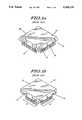
- Pin grid array packageshave become a popular form of integrated circuit packaging, as they provide for a large number of pins in a plug-in type package.
- An array of pins having a standard spacing(for example, 100 mils center to center) is located on a ceramic substrate so that the pins extends outward from one face of the substrate to join with sockets on a main printed circuit board.
- An integrated circuit or semiconductor deviceis mounted on the top side of the ceramic substrate and wire bonds are made between the bonding pads of the integrated circuit and the traces on the substrate. The integrated circuit, the leads, and the wire bonds are then covered with an encapsulant to complete the package.
- the integrated circuit chip and associated interconnectionsare encapsulated in a plastic resin, as in glob top or chip-on-board technology.
- the assemblyis encapsulated by transfer molding a thermoset plastic composition over the device and the ceramic substrate.
- transfer moldingthe assembly to be encapsulated is located inside a metal mold which has recesses defining the shape of the cover to be produced. Solid plastic is heated and forced under pressure through gates into the mold. The heat and pressure causes the plastic to liquify and flow into the mold cavities surrounding the integrated circuit. The mold is heated to cure the plastic and the molded assembly is then removed from the mold.
- the basic characteristics of transfer moldingare taught in U.S. Pat. No. 4,460,537.
- the structure of a plastic pin grid array assemblyis similar to its ceramic equivalent. Instead of using a ceramic substrate, low-cost materials such as epoxy-glass or polyester-glass printed circuit boards are used for the substrate. The fabrication of these substrates shares most of the same assembly processes and techniques with conventional printed circuit board manufacturing processes. The pins of the package are inserted into plated-through holes in the circuit board and either press-fit or reflow soldered.
- plastic molded pin grid arrays 10are formed about a substrate 12 containing an array of pins 14 extending from the bottom of the substrate 12.
- a plastic compound 16is transfer-molded about the substrate to form a completed package.
- the substrateis registered in the mold by locating the edges of the substrate 12 against registration bumps in the mold. After the molding is completed, the registration bumps appear in the finished pin grid array package as indentations or ribs 13.
- Alternate methods and configurations of forming molded pin grid array packagesemploy slanted side walls 18 to aid in removal of the molded part from the molding press. Such a transfer-molded plastic pin grid array package is taught in U.S. Pat. No. 4,935,581.
- a pad array chip carrier packagecomprising a resinous circuit carrying substrate having an array of solder pads on the bottom side and a semiconductor device electrically and mechanically mounted on the top side.
- a protective plastic coveris transfer molded about the semiconductor device, covering substantially all of the top side of the circuit carrying substrate.
- solder bumpsare formed on the solder pads in order to provide a pad array chip carrier package that is easily soldered to a main circuit board.
- a metal stiffeneris bonded to the circuit carrying substrate under the semiconductor device.
- the semiconductor deviceis electrically connected to the substrate and a cover is transfer molded about the semiconductor device, covering substantially all of the top side of the circuit carrying substrate.
- FIG. 1ais a perspective view of a prior art pin grid array package.
- FIG. 1bis a perspective view of a prior art pin grid array package.
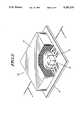
- FIG. 2is a perspective cut-away view of a resin-molded pad array chip carrier in accordance with the present invention.
- FIG. 3is a plan view of the bottom of a pad array chip carrier in accordance with the present invention.
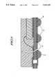
- FIG. 4is a fragmentary sectional view of FIGS. 2 and 3 through section AA.
- FIG. 5is the same fragmentary sectional view of an alternate embodiment of the invention.
- FIG. 6is the same fragmentary sectional view of another embodiment of the invention.
- a leadless, transfer-molded, pad array chip carrier 20is made by placing an integrated circuit chip or semiconductor device 24 on a circuit-carrying substrate 22.
- the circuit carrying substrateis a resinous printed circuit board such as epoxy-glass or polyimide-glass, but may also consist of other materials such as flexible circuitry made from polyimide, polyester, or polyetherimide film.
- the substrate 22has a metallization pattern 25 on the upper surface of the substrate.
- the integrated circuit 24is adhesively bonded or eutectic bonded to the substrate 22 and wire-bonded to the metallization pattern 25.
- the integrated circuit 24may also be attached to the substrate 22 by flip-chip bonding or by tape-automated-bonding (TAB). The substrate and chip assembly is then placed into a molding machine.
- TABtape-automated-bonding
- a transfer molding machineis used, but other methods of molding such as injection molding or reaction injection molding (RIM) may be employed, depending on the materials selected.
- Transfer moldingutilizes thermosetting materials
- injection moldingutilizes thermoplastic materials
- RIMutilizes materials that are thermoplastic but react within the mold to form thermosets.
- a cover 26is molded about the chip in order to encapsulate and cover the chip and all the associated interconnections.
- the molding compound 26may extend to the edges of the substrate 22 but will preferably terminate at a distance from the edges of the substrate 22 in order to provide a means for holding or securing the substrate while it is in the mold. By extending the substrate 22 beyond the body of the molding compound 26, the need to have notches or ribs in the molded body (as in the prior art) is obviated.
- the bottom side of the substrate 22contains an array 35 of solder pads 34 arranged in a particular configuration (see FIG. 3).
- the solder padsare typically circular but may assume other shapes.
- the solder pads 34serve to provide the electrical interconnection between the pad array chip carrier and a main circuit board (not shown).
- the solder pads 34are made from the same metallization as the remainder of the circuit board, typically copper, and may be coated with another material such as gold to prevent oxidation of the solder pads. If the pad array chip carrier is to be soldered to the main printed circuit board, the solder pads may be coated with solder plating or reflowed with solder paste, solder spheres, or other methods to create solder bumps on the solder pads.
- the substrate 22contains a chip bonding metallization pad 43 to which the chip 24 is attached using a conductive adhesive 47. Other means of attachment, such as eutectic bonding, may also be used.
- the chipis electrically wire-bonded by thin metal wires 49, typically gold or aluminum, to the metallization pattern 25.
- the electrical connection from the metallization pattern 25 to the solder pads 34is effected with plated-through-holes 42.
- the metallization pattern 25 on the top surface of the printed circuit boardterminates as an annular ring at a plated-through-hole 42.
- the electrical connection on the bottom side of the printed circuit boardis made by connecting the plated-through-hole 42 to another annular ring and extending the metallization pattern to the solder pads 34.
- a solder mask 41is placed over the metallization patterns and plated-through-holes 42, but may be eliminated or only partially employed as required.
- the assemblyis transfer-molded using a thermoplastic or thermoset molding compound, preferably a thermoset epoxy.
- the molding compound 26encapsulates the chip 24 and wire-bonds 49, and covers nearly all the top surface of the printed circuit board 22. It can be seen that the upper surface of the printed circuit board is not totally covered by the molding compound, but a small portion around the peripheral edge of the molding compound is left exposed in order to facilitate fixturing the assembly in the mold and subsequent handling during assembly operations.
- the exposed portion of the circuit boardcan be on one, two, three, or all four sides of the cover.
- FIG. 5An alternate embodiment of the invention (FIG. 5) employs solder bumps 52 on the solder pads 54 to create a array of bumped solder pads.
- solder bumpsallows the pad array chip carrier to be easily soldered to the solder pads on the main circuit board (not shown).
- the height of the solder bumpmust be sufficient to effect a surface mount interconnect, typically from about 3 to about 30 mils high, and of about the same diameter as the solder pad 54.
- a further embodiment of the inventionemploys a metal member or stiffener 60 made from a thin sheet of a material such as steel, nickel, copper clad invar, alloy 42, or other materials having a flexural modulus in excess of about 2,000,000 psi.
- the thickness of the stiffenervaries from about 3 to about 10 mils depending of the type of material used.
- the stiffeneris adhesively bonded to the pad 63 of the printed circuit board 62 using an adhesive material 68.
- the chip 64is then attached to the stiffener 60 using a conductive adhesive 67 as in the previous example.
- the metal stiffeneracts to reduce the mechanical stress imparted by the mismatch between the thermal expansion coefficients of the printed circuit board and the silicon chip.
- a cover 66is molded as in the previous example to encapsulate the integrated circuit 64, the wire bonds 69, the stiffener 60, and the top surface of the printed circuit board 62.
Landscapes
- Engineering & Computer Science (AREA)
- Microelectronics & Electronic Packaging (AREA)
- Computer Hardware Design (AREA)
- Power Engineering (AREA)
- Physics & Mathematics (AREA)
- Condensed Matter Physics & Semiconductors (AREA)
- General Physics & Mathematics (AREA)
- Wire Bonding (AREA)
Abstract
Description
Claims (11)
Priority Applications (1)
| Application Number | Priority Date | Filing Date | Title |
|---|---|---|---|
| US07/976,720US5241133A (en) | 1990-12-21 | 1992-11-16 | Leadless pad array chip carrier |
Applications Claiming Priority (2)
| Application Number | Priority Date | Filing Date | Title |
|---|---|---|---|
| US63184890A | 1990-12-21 | 1990-12-21 | |
| US07/976,720US5241133A (en) | 1990-12-21 | 1992-11-16 | Leadless pad array chip carrier |
Related Parent Applications (1)
| Application Number | Title | Priority Date | Filing Date |
|---|---|---|---|
| US63184890AContinuation | 1990-12-21 | 1990-12-21 |
Publications (1)
| Publication Number | Publication Date |
|---|---|
| US5241133Atrue US5241133A (en) | 1993-08-31 |
Family
ID=27091492
Family Applications (1)
| Application Number | Title | Priority Date | Filing Date |
|---|---|---|---|
| US07/976,720Expired - LifetimeUS5241133A (en) | 1990-12-21 | 1992-11-16 | Leadless pad array chip carrier |
Country Status (1)
| Country | Link |
|---|---|
| US (1) | US5241133A (en) |
Cited By (174)
| Publication number | Priority date | Publication date | Assignee | Title |
|---|---|---|---|---|
| US5355283A (en)* | 1993-04-14 | 1994-10-11 | Amkor Electronics, Inc. | Ball grid array with via interconnection |
| US5396032A (en)* | 1993-05-04 | 1995-03-07 | Alcatel Network Systems, Inc. | Method and apparatus for providing electrical access to devices in a multi-chip module |
| US5426263A (en)* | 1993-12-23 | 1995-06-20 | Motorola, Inc. | Electronic assembly having a double-sided leadless component |
| EP0664562A1 (en)* | 1994-01-12 | 1995-07-26 | AT&T Corp. | Ball grid array plastic package |
| US5442230A (en)* | 1994-09-16 | 1995-08-15 | National Semiconductor Corporation | High density integrated circuit assembly combining leadframe leads with conductive traces |
| US5444303A (en)* | 1994-08-10 | 1995-08-22 | Motorola, Inc. | Wire bond pad arrangement having improved pad density |
| US5446625A (en)* | 1993-11-10 | 1995-08-29 | Motorola, Inc. | Chip carrier having copper pattern plated with gold on one surface and devoid of gold on another surface |
| NL9500511A (en)* | 1994-03-16 | 1995-11-01 | Amkor Electronics | Mold runner removal of a substrate-based, encapsulated, electronic building block. |
| US5471011A (en)* | 1994-05-26 | 1995-11-28 | Ak Technology, Inc. | Homogeneous thermoplastic semi-conductor chip carrier package |
| US5473512A (en)* | 1993-12-16 | 1995-12-05 | At&T Corp. | Electronic device package having electronic device boonded, at a localized region thereof, to circuit board |
| US5512710A (en)* | 1992-08-21 | 1996-04-30 | Cts Corporation | Multilayer package with second layer via test connections |
| US5535101A (en)* | 1992-11-03 | 1996-07-09 | Motorola, Inc. | Leadless integrated circuit package |
| US5552636A (en)* | 1993-06-01 | 1996-09-03 | Motorola, Inc. | Discrete transitor assembly |
| FR2734948A1 (en)* | 1995-05-31 | 1996-12-06 | Sgs Thomson Microelectronics | ENCAPSULATION BOX WITH WELDING BALL ARRAY AND ENCAPSULATION METHOD. |
| FR2734947A1 (en)* | 1995-05-31 | 1996-12-06 | Sgs Thomson Microelectronics | ENCAPSULATION BOX WITH WELDING BALL ARRAY AND ENCAPSULATION METHOD. |
| US5583378A (en)* | 1994-05-16 | 1996-12-10 | Amkor Electronics, Inc. | Ball grid array integrated circuit package with thermal conductor |
| US5583747A (en)* | 1993-11-01 | 1996-12-10 | Baird; John H. | Thermoplastic interconnect for electronic device and method for making |
| US5591941A (en)* | 1993-10-28 | 1997-01-07 | International Business Machines Corporation | Solder ball interconnected assembly |
| US5596485A (en)* | 1995-03-16 | 1997-01-21 | Amkor Electronics, Inc. | Plastic packaged integrated circuit with heat spreader |
| EP0729182A3 (en)* | 1995-02-23 | 1997-02-19 | Matsushita Electric Industrial Co Ltd | Chip carrier, associated manufacturing and assembly |
| US5609889A (en)* | 1995-05-26 | 1997-03-11 | Hestia Technologies, Inc. | Apparatus for encapsulating electronic packages |
| US5615089A (en)* | 1994-07-26 | 1997-03-25 | Fujitsu Limited | BGA semiconductor device including a plurality of semiconductor chips located on upper and lower surfaces of a first substrate |
| US5625224A (en)* | 1994-08-10 | 1997-04-29 | Motorola, Inc. | Method and apparatus for an integrated circuit chip carrier having improved mounting pad density |
| EP0772233A1 (en) | 1995-10-30 | 1997-05-07 | STMicroelectronics S.A. | A solder ball array package |
| US5628919A (en)* | 1993-12-13 | 1997-05-13 | Matsushita Electric Industrial Co., Ltd. | Methods for producing a chip carrier and terminal electrode for a circuit substrate |
| US5629835A (en)* | 1994-07-19 | 1997-05-13 | Olin Corporation | Metal ball grid array package with improved thermal conductivity |
| EP0778616A2 (en) | 1995-12-05 | 1997-06-11 | Lucent Technologies Inc. | Method of packaging devices with a gel medium confined by a rim member |
| EP0778617A2 (en) | 1995-12-05 | 1997-06-11 | Lucent Technologies Inc. | Electronic device package enclosed by pliant medium laterally confined by a plastic rim member |
| US5640047A (en)* | 1995-09-25 | 1997-06-17 | Mitsui High-Tec, Inc. | Ball grid assembly type semiconductor device having a heat diffusion function and an electric and magnetic shielding function |
| US5650593A (en)* | 1994-05-26 | 1997-07-22 | Amkor Electronics, Inc. | Thermally enhanced chip carrier package |
| US5652463A (en)* | 1995-05-26 | 1997-07-29 | Hestia Technologies, Inc. | Transfer modlded electronic package having a passage means |
| KR970053689A (en)* | 1995-12-30 | 1997-07-31 | 황인길 | Structure and Manufacturing Method of Chip Size Package |
| US5686699A (en)* | 1995-10-10 | 1997-11-11 | Acc Microelectronics Corporation | Semiconductor board providing high signal pin utilization |
| US5696666A (en)* | 1995-10-11 | 1997-12-09 | Motorola, Inc. | Low profile exposed die chip carrier package |
| US5703402A (en)* | 1995-11-13 | 1997-12-30 | Acc Microelectronics Corporation | Output mapping of die pad bonds in a ball grid array |
| US5729438A (en)* | 1996-06-07 | 1998-03-17 | Motorola, Inc. | Discrete component pad array carrier |
| US5748452A (en)* | 1996-07-23 | 1998-05-05 | International Business Machines Corporation | Multi-electronic device package |
| EP0840374A1 (en) | 1996-10-30 | 1998-05-06 | STMicroelectronics S.A. | A semiconductor package having mechanically and electrically bonded supportive elements |
| US5796163A (en)* | 1997-05-23 | 1998-08-18 | Amkor Technology, Inc. | Solder ball joint |
| US5796589A (en)* | 1995-12-20 | 1998-08-18 | Intel Corporation | Ball grid array integrated circuit package that has vias located within the solder pads of a package |
| US5801440A (en)* | 1995-10-10 | 1998-09-01 | Acc Microelectronics Corporation | Chip package board having utility rings |
| US5820014A (en) | 1993-11-16 | 1998-10-13 | Form Factor, Inc. | Solder preforms |
| US5827999A (en)* | 1994-05-26 | 1998-10-27 | Amkor Electronics, Inc. | Homogeneous chip carrier package |
| US5829988A (en)* | 1996-11-14 | 1998-11-03 | Amkor Electronics, Inc. | Socket assembly for integrated circuit chip carrier package |
| US5844315A (en)* | 1996-03-26 | 1998-12-01 | Motorola Corporation | Low-profile microelectronic package |
| US5854512A (en)* | 1996-09-20 | 1998-12-29 | Vlsi Technology, Inc. | High density leaded ball-grid array package |
| US5856912A (en)* | 1997-03-04 | 1999-01-05 | Motorola Inc. | Microelectronic assembly for connection to an embedded electrical element, and method for forming same |
| US5866949A (en)* | 1996-12-02 | 1999-02-02 | Minnesota Mining And Manufacturing Company | Chip scale ball grid array for integrated circuit packaging |
| US5875011A (en)* | 1997-04-10 | 1999-02-23 | International Business Machines Corporation | Liquid crystal display tile interconnected to a tile carrier and method |
| US5895976A (en)* | 1996-06-03 | 1999-04-20 | Motorola Corporation | Microelectronic assembly including polymeric reinforcement on an integrated circuit die, and method for forming same |
| US5898215A (en)* | 1996-12-16 | 1999-04-27 | Motorola, Inc. | Microelectronic assembly with connection to a buried electrical element, and method for forming same |
| US5904497A (en)* | 1997-08-22 | 1999-05-18 | Micron Technology, Inc. | Method and apparatus for semiconductor assembly which includes testing of chips and replacement of bad chips prior to final assembly |
| US5920117A (en)* | 1994-08-02 | 1999-07-06 | Fujitsu Limited | Semiconductor device and method of forming the device |
| US5950074A (en)* | 1997-04-18 | 1999-09-07 | Amkor Technology, Inc. | Method of making an integrated circuit package |
| US5952719A (en)* | 1995-07-14 | 1999-09-14 | Advanced Interconnect Technologies, Inc. | Metal ball grid electronic package having improved solder joint |
| US5962810A (en)* | 1997-09-09 | 1999-10-05 | Amkor Technology, Inc. | Integrated circuit package employing a transparent encapsulant |
| US5962917A (en)* | 1997-03-31 | 1999-10-05 | Nec Corporation | Semiconductor device package having end-face halved through-holes and inside-area through-holes |
| US5981314A (en)* | 1996-10-31 | 1999-11-09 | Amkor Technology, Inc. | Near chip size integrated circuit package |
| US5990545A (en)* | 1996-12-02 | 1999-11-23 | 3M Innovative Properties Company | Chip scale ball grid array for integrated circuit package |
| US5994152A (en) | 1996-02-21 | 1999-11-30 | Formfactor, Inc. | Fabricating interconnects and tips using sacrificial substrates |
| US6002169A (en)* | 1998-06-15 | 1999-12-14 | Lsi Logic Corporation | Thermally enhanced tape ball grid array package |
| US6002178A (en)* | 1997-11-12 | 1999-12-14 | Lin; Paul T. | Multiple chip module configuration to simplify testing process and reuse of known-good chip-size package (CSP) |
| US6004833A (en)* | 1998-04-21 | 1999-12-21 | Atmel Corporation | Method for constructing a leadless array package |
| US6015955A (en)* | 1997-06-20 | 2000-01-18 | International Business Machines Corporation | Reworkability solution for wirebound chips using high performance capacitor |
| US6031284A (en)* | 1997-03-14 | 2000-02-29 | Lg Semicon Co., Ltd. | Package body and semiconductor chip package using same |
| US6054338A (en)* | 1996-05-17 | 2000-04-25 | National Semiconductor Corporation | Low cost ball grid array device and method of manufacture thereof |
| US6100597A (en)* | 1996-11-15 | 2000-08-08 | Nec Corporation | Semiconductor device and method for manufacturing the same |
| US6100596A (en)* | 1996-03-19 | 2000-08-08 | Methode Electronics, Inc. | Connectorized substrate and method of connectorizing a substrate |
| US6111324A (en)* | 1998-02-05 | 2000-08-29 | Asat, Limited | Integrated carrier ring/stiffener and method for manufacturing a flexible integrated circuit package |
| US6114770A (en)* | 1998-07-22 | 2000-09-05 | Micron Technology, Inc. | Low profile semiconductor package |
| US6117705A (en)* | 1997-04-18 | 2000-09-12 | Amkor Technology, Inc. | Method of making integrated circuit package having adhesive bead supporting planar lid above planar substrate |
| US6120885A (en)* | 1997-07-10 | 2000-09-19 | International Business Machines Corporation | Structure, materials, and methods for socketable ball grid |
| US6130383A (en)* | 1995-05-31 | 2000-10-10 | Sgs-Thomson Microelectronics, S.A. | Solder ball array package and a method of encapsulation |
| US6133627A (en) | 1990-09-24 | 2000-10-17 | Tessera, Inc. | Semiconductor chip package with center contacts |
| US6150193A (en)* | 1996-10-31 | 2000-11-21 | Amkor Technology, Inc. | RF shielded device |
| US6158116A (en)* | 1996-06-13 | 2000-12-12 | Matsushita Electric Industrial Co., Ltd. | Radio frequency module and method for fabricating the radio frequency module |
| US6172423B1 (en) | 1997-11-15 | 2001-01-09 | Hyundai Electronics Industries Co., Ltd. | Layer-type ball grid array semiconductor package and fabrication method thereof |
| US6177726B1 (en)* | 1999-02-11 | 2001-01-23 | Philips Electronics North America Corporation | SiO2 wire bond insulation in semiconductor assemblies |
| US6194250B1 (en) | 1998-09-14 | 2001-02-27 | Motorola, Inc. | Low-profile microelectronic package |
| EP0926730A3 (en)* | 1997-12-19 | 2001-03-21 | Texas Instruments Incorporated | Ball grid array package and method of construction thereof |
| KR20010045373A (en)* | 1999-11-04 | 2001-06-05 | 마이클 디. 오브라이언 | Semiconductor |
| US6262477B1 (en) | 1993-03-19 | 2001-07-17 | Advanced Interconnect Technologies | Ball grid array electronic package |
| US6274823B1 (en) | 1993-11-16 | 2001-08-14 | Formfactor, Inc. | Interconnection substrates with resilient contact structures on both sides |
| US6281096B1 (en) | 1999-04-22 | 2001-08-28 | International Rectifier Corp. | Chip scale packaging process |
| US6297559B1 (en) | 1997-07-10 | 2001-10-02 | International Business Machines Corporation | Structure, materials, and applications of ball grid array interconnections |
| US20010030370A1 (en)* | 1990-09-24 | 2001-10-18 | Khandros Igor Y. | Microelectronic assembly having encapsulated wire bonding leads |
| US6316837B1 (en) | 1997-12-04 | 2001-11-13 | Hyundai Electronics Industries Co., Ltd. | Area array type semiconductor package and fabrication method |
| US6337522B1 (en) | 1997-07-10 | 2002-01-08 | International Business Machines Corporation | Structure employing electrically conductive adhesives |
| USD453142S1 (en) | 2000-04-24 | 2002-01-29 | Tamura Corporation | Circuit block for power supply |
| USD453141S1 (en) | 2000-04-24 | 2002-01-29 | Tamura Coroportion | Circuit block for power supply |
| US6355199B1 (en) | 1999-02-12 | 2002-03-12 | St. Assembly Test Services Pte Ltd | Method of molding flexible circuit with molded stiffener |
| US6365979B1 (en)* | 1998-03-06 | 2002-04-02 | Kabushiki Kaisha Toshiba | Semiconductor device and manufacturing method thereof |
| US6373139B1 (en) | 1999-10-06 | 2002-04-16 | Motorola, Inc. | Layout for a ball grid array |
| US6388887B1 (en) | 1993-12-27 | 2002-05-14 | Hitachi, Ltd. | Surface mount type package unit |
| US6418029B1 (en) | 2000-02-28 | 2002-07-09 | Mckee James S. | Interconnect system having vertically mounted passive components on an underside of a substrate |
| US6429530B1 (en) | 1998-11-02 | 2002-08-06 | International Business Machines Corporation | Miniaturized chip scale ball grid array semiconductor package |
| US6441498B1 (en) | 1997-12-02 | 2002-08-27 | Hyundai Electronics Industries Co., Ltd. | Semiconductor substrate and land grid array semiconductor package using same |
| US6448635B1 (en) | 1999-08-30 | 2002-09-10 | Amkor Technology, Inc. | Surface acoustical wave flip chip |
| US20020124392A1 (en)* | 1998-10-15 | 2002-09-12 | Chung Kevin Kwong-Tai | Method for making an article having an embedded electronic device |
| US6472598B1 (en) | 1998-08-28 | 2002-10-29 | Amkor Technology, Inc. | Electromagnetic interference shield device with conductive encapsulant and dam |
| US6479901B1 (en) | 1998-12-21 | 2002-11-12 | Oki Electric Industry Co., Ltd. | Semiconductor device having interconnected external electrode pads and wire bonding pads |
| US20020168798A1 (en)* | 1996-10-31 | 2002-11-14 | Glenn Thomas P. | Method of making near chip size integrated circuit package |
| US6538307B1 (en)* | 2000-06-28 | 2003-03-25 | Advanced Micro Devices, Inc. | Packaging substrate comprising staggered vias |
| US6551862B2 (en)* | 2000-11-02 | 2003-04-22 | Hitachi, Ltd. | Semiconductor device and method of manufacturing the same |
| US6551112B1 (en) | 2002-03-18 | 2003-04-22 | High Connection Density, Inc. | Test and burn-in connector |
| DE19719983C2 (en)* | 1996-05-17 | 2003-05-15 | Nat Semiconductor Corp | Mounting plate for semiconductor devices and method for the production thereof |
| US20030137039A1 (en)* | 2001-11-16 | 2003-07-24 | Tdk Corporation | Packaging substrate and manufacturing method thereof, integrated circuit device and manufacturing method thereof, and saw device |
| US6624005B1 (en) | 2000-09-06 | 2003-09-23 | Amkor Technology, Inc. | Semiconductor memory cards and method of making same |
| US6634726B1 (en) | 2001-05-30 | 2003-10-21 | Snap-On Technologies, Inc. | Multiple drawer cabinet allowing one drawer opened at a time |
| US6653740B2 (en) | 2000-02-10 | 2003-11-25 | International Rectifier Corporation | Vertical conduction flip-chip device with bump contacts on single surface |
| US20040005733A1 (en)* | 1997-07-30 | 2004-01-08 | Atsushi Fujisawa | Method of manufacturing semiconductor device |
| US6686226B1 (en)* | 1994-02-10 | 2004-02-03 | Hitachi, Ltd. | Method of manufacturing a semiconductor device a ball grid array package structure using a supporting frame |
| US20040022043A1 (en)* | 2002-07-16 | 2004-02-05 | Murata Manufacturing Co., Ltd. | Laminated ceramic electronic component and method of producing the same |
| US20040041248A1 (en)* | 2002-09-04 | 2004-03-04 | Kieran Harney | Packaged microchip with isolation |
| US20040041254A1 (en)* | 2002-09-04 | 2004-03-04 | Lewis Long | Packaged microchip |
| US6716670B1 (en) | 2002-01-09 | 2004-04-06 | Bridge Semiconductor Corporation | Method of forming a three-dimensional stacked semiconductor package device |
| US20040119143A1 (en)* | 2002-12-19 | 2004-06-24 | Karpman Maurice S. | Packaged microchip with isolator having selected modulus of elasticity |
| US20040150083A1 (en)* | 2000-05-10 | 2004-08-05 | Samsung Electronic Co., Ltd. | Method for manufacturing digital micro-mirror device (DMD) |
| US20040164411A1 (en)* | 1999-05-07 | 2004-08-26 | Amkor Technology, Inc. | Semiconductor package and method for fabricating the same |
| US20040175916A1 (en)* | 1999-05-20 | 2004-09-09 | Amkor Technology, Inc. | Stackable semiconductor package having semiconductor chip within central through hole of substrate |
| US20050035446A1 (en)* | 2002-09-04 | 2005-02-17 | Karpman Maurice S. | Packaged microchip with premolded-type package |
| US20050056870A1 (en)* | 2002-12-19 | 2005-03-17 | Karpman Maurice S. | Stress sensitive microchip with premolded-type package |
| US20050127498A1 (en)* | 2001-11-13 | 2005-06-16 | Masazumi Amagai | Copper-based chip attach for chip-scale semiconductor packages |
| US6936495B1 (en) | 2002-01-09 | 2005-08-30 | Bridge Semiconductor Corporation | Method of making an optoelectronic semiconductor package device |
| US6987034B1 (en) | 2002-01-09 | 2006-01-17 | Bridge Semiconductor Corporation | Method of making a semiconductor package device that includes singulating and trimming a lead |
| US20060040488A1 (en)* | 1994-12-29 | 2006-02-23 | Tessera, Inc. | Method of electrically connecting a microelectronic component |
| US20060079027A1 (en)* | 2002-05-16 | 2006-04-13 | Renesas Technology Corporation | Semiconductor device and its manufacturing method |
| US7098078B2 (en) | 1990-09-24 | 2006-08-29 | Tessera, Inc. | Microelectronic component and assembly having leads with offset portions |
| US7190060B1 (en) | 2002-01-09 | 2007-03-13 | Bridge Semiconductor Corporation | Three-dimensional stacked semiconductor package device with bent and flat leads and method of making same |
| US20070134843A1 (en)* | 2005-12-12 | 2007-06-14 | Fujitsu Limited | Semiconductor device and method for fabricating the same |
| US20070145548A1 (en)* | 2003-12-22 | 2007-06-28 | Amkor Technology, Inc. | Stack-type semiconductor package and manufacturing method thereof |
| US20070158841A1 (en)* | 2006-01-12 | 2007-07-12 | Powertech Technology Inc. | Structure of Ball Grid Array package |
| US20070205496A1 (en)* | 2004-06-25 | 2007-09-06 | Tessera, Inc. | Microelectronic packages and methods therefor |
| US20070235886A1 (en)* | 2006-04-06 | 2007-10-11 | Hamza Yilmaz | Semiconductor die packages using thin dies and metal substrates |
| US20080029207A1 (en)* | 2006-07-20 | 2008-02-07 | Smith Timothy J | Insert Molded Actuator Components |
| US20080042252A1 (en)* | 1998-06-30 | 2008-02-21 | Micron Technology, Inc. | Stackable ceramic fbga for high thermal applications |
| USRE40112E1 (en) | 1999-05-20 | 2008-02-26 | Amkor Technology, Inc. | Semiconductor package and method for fabricating the same |
| EP1041628A3 (en)* | 1999-03-29 | 2008-05-28 | Interuniversitair Microelektronica Centrum Vzw | An image sensor ball grid array package and the fabrication thereof |
| US20080150101A1 (en)* | 2006-12-20 | 2008-06-26 | Tessera, Inc. | Microelectronic packages having improved input/output connections and methods therefor |
| US20080157298A1 (en)* | 2006-06-29 | 2008-07-03 | Analog Devices, Inc. | Stress Mitigation in Packaged Microchips |
| US20090000428A1 (en)* | 2007-06-27 | 2009-01-01 | Siemens Medical Solution Usa, Inc. | Photo-Multiplier Tube Removal Tool |
| US20090145641A1 (en)* | 2007-12-11 | 2009-06-11 | Palo Alto Research Center Incorporated | Combining discrete electronic elements with printed electronic circuits |
| US7601039B2 (en) | 1993-11-16 | 2009-10-13 | Formfactor, Inc. | Microelectronic contact structure and method of making same |
| US20090267171A1 (en)* | 2008-04-24 | 2009-10-29 | Micron Technology, Inc. | Pre-encapsulated cavity interposer |
| US20090284941A1 (en)* | 2008-05-15 | 2009-11-19 | Kouji Oomori | Semiconductor package, mounting circuit board, and mounting structure |
| US20100187557A1 (en)* | 2009-01-28 | 2010-07-29 | Samoilov Arkadii V | Light Sensor Using Wafer-Level Packaging |
| US8033838B2 (en) | 1996-02-21 | 2011-10-11 | Formfactor, Inc. | Microelectronic contact structure |
| US20120161306A1 (en)* | 2010-12-23 | 2012-06-28 | Atmel Corporation | Semiconductor Package |
| US20120287582A1 (en)* | 2011-05-11 | 2012-11-15 | Patrizio Vinciarelli | Panel-Molded Electronic Assemblies |
| US20130277847A1 (en)* | 2012-04-18 | 2013-10-24 | Hon Hai Precision Industry Co., Ltd. | Chip package and method for assembling chip package |
| US8588017B2 (en) | 2010-10-20 | 2013-11-19 | Samsung Electronics Co., Ltd. | Memory circuits, systems, and modules for performing DRAM refresh operations and methods of operating the same |
| US8940629B2 (en) | 2010-09-22 | 2015-01-27 | Seiko Instruments Inc. | Ball grid array semiconductor package and method of manufacturing the same |
| US20150092356A1 (en)* | 2013-10-02 | 2015-04-02 | Ibiden Co., Ltd. | Printed wiring board, method for manufacturing printed wiring board and package-on-package |
| US9006880B1 (en) | 2000-11-28 | 2015-04-14 | Knowles Electronics, Llc | Top port multi-part surface mount silicon condenser microphone |
| US9040360B1 (en) | 2000-11-28 | 2015-05-26 | Knowles Electronics, Llc | Methods of manufacture of bottom port multi-part surface mount MEMS microphones |
| US9078063B2 (en) | 2012-08-10 | 2015-07-07 | Knowles Electronics, Llc | Microphone assembly with barrier to prevent contaminant infiltration |
| US9137903B2 (en) | 2010-12-21 | 2015-09-15 | Tessera, Inc. | Semiconductor chip assembly and method for making same |
| US9374643B2 (en) | 2011-11-04 | 2016-06-21 | Knowles Electronics, Llc | Embedded dielectric as a barrier in an acoustic device and method of manufacture |
| US9402319B2 (en) | 2011-05-11 | 2016-07-26 | Vlt, Inc. | Panel-molded electronic assemblies |
| US9466545B1 (en) | 2007-02-21 | 2016-10-11 | Amkor Technology, Inc. | Semiconductor package in package |
| US20170053884A1 (en)* | 2015-08-17 | 2017-02-23 | Mediatek Inc. | Structure and layout of ball grid array packages |
| US9676614B2 (en) | 2013-02-01 | 2017-06-13 | Analog Devices, Inc. | MEMS device with stress relief structures |
| US9794661B2 (en) | 2015-08-07 | 2017-10-17 | Knowles Electronics, Llc | Ingress protection for reducing particle infiltration into acoustic chamber of a MEMS microphone package |
| US9936580B1 (en) | 2015-01-14 | 2018-04-03 | Vlt, Inc. | Method of forming an electrical connection to an electronic module |
| US9967984B1 (en) | 2015-01-14 | 2018-05-08 | Vlt, Inc. | Power adapter packaging |
| US10131538B2 (en) | 2015-09-14 | 2018-11-20 | Analog Devices, Inc. | Mechanically isolated MEMS device |
| US10167189B2 (en) | 2014-09-30 | 2019-01-01 | Analog Devices, Inc. | Stress isolation platform for MEMS devices |
| US10264664B1 (en) | 2015-06-04 | 2019-04-16 | Vlt, Inc. | Method of electrically interconnecting circuit assemblies |
| US20210082871A1 (en)* | 2019-09-17 | 2021-03-18 | Taiwan Semiconductor Manufacturing Company, Ltd. | Semiconductor devices and methods of manufacturing |
| US20210219418A1 (en)* | 2020-01-13 | 2021-07-15 | Juniper Networks, Inc. | Apparatus, system, and method for increased current distribution on high-density circuit boards |
| US11137241B2 (en)* | 2019-03-27 | 2021-10-05 | Vishay Advanced Technologies, Ltd. | Three dimensional strain gage |
| US20210323813A1 (en)* | 2018-03-01 | 2021-10-21 | Infineon Technologies Ag | MEMS-Sensor |
| US11417611B2 (en) | 2020-02-25 | 2022-08-16 | Analog Devices International Unlimited Company | Devices and methods for reducing stress on circuit components |
| US11981560B2 (en) | 2020-06-09 | 2024-05-14 | Analog Devices, Inc. | Stress-isolated MEMS device comprising substrate having cavity and method of manufacture |
Citations (13)
| Publication number | Priority date | Publication date | Assignee | Title |
|---|---|---|---|---|
| JPS5779652A (en)* | 1980-11-05 | 1982-05-18 | Nec Corp | Resin-sealed semiconductor device |
| US4460537A (en)* | 1982-07-26 | 1984-07-17 | Motorola, Inc. | Slot transfer molding apparatus and methods |
| US4688152A (en)* | 1986-08-11 | 1987-08-18 | National Semiconductor Corporation | Molded pin grid array package GPT |
| JPS62274735A (en)* | 1986-05-23 | 1987-11-28 | Hitachi Ltd | Tape carrier type package mountable in hole |
| JPS63283147A (en)* | 1987-05-15 | 1988-11-21 | Seiko Keiyo Kogyo Kk | Semiconductor device |
| US4822550A (en)* | 1986-04-17 | 1989-04-18 | Citizen Watch Co., Ltd. | Method of molding a protective cover on a pin grid array |
| JPH0251165A (en)* | 1988-08-15 | 1990-02-21 | Mitsui Toatsu Chem Inc | Magenta color toner composition |
| JPH02128453A (en)* | 1988-11-08 | 1990-05-16 | Toppan Printing Co Ltd | IC module for IC card and its manufacturing method |
| US4935581A (en)* | 1986-04-17 | 1990-06-19 | Citizen Watch Co., Ltd. | Pin grid array package |
| US4961105A (en)* | 1986-02-06 | 1990-10-02 | Hitachi Maxell, Ltd | Arrangement of a semiconductor device for use in a card |
| US4975765A (en)* | 1988-07-22 | 1990-12-04 | Contraves Ag | Highly integrated circuit and method for the production thereof |
| US5019673A (en)* | 1990-08-22 | 1991-05-28 | Motorola, Inc. | Flip-chip package for integrated circuits |
| US5107329A (en)* | 1988-02-26 | 1992-04-21 | Hitachi, Ltd. | Pin-grid array semiconductor device |
- 1992
- 1992-11-16USUS07/976,720patent/US5241133A/ennot_activeExpired - Lifetime
Patent Citations (13)
| Publication number | Priority date | Publication date | Assignee | Title |
|---|---|---|---|---|
| JPS5779652A (en)* | 1980-11-05 | 1982-05-18 | Nec Corp | Resin-sealed semiconductor device |
| US4460537A (en)* | 1982-07-26 | 1984-07-17 | Motorola, Inc. | Slot transfer molding apparatus and methods |
| US4961105A (en)* | 1986-02-06 | 1990-10-02 | Hitachi Maxell, Ltd | Arrangement of a semiconductor device for use in a card |
| US4822550A (en)* | 1986-04-17 | 1989-04-18 | Citizen Watch Co., Ltd. | Method of molding a protective cover on a pin grid array |
| US4935581A (en)* | 1986-04-17 | 1990-06-19 | Citizen Watch Co., Ltd. | Pin grid array package |
| JPS62274735A (en)* | 1986-05-23 | 1987-11-28 | Hitachi Ltd | Tape carrier type package mountable in hole |
| US4688152A (en)* | 1986-08-11 | 1987-08-18 | National Semiconductor Corporation | Molded pin grid array package GPT |
| JPS63283147A (en)* | 1987-05-15 | 1988-11-21 | Seiko Keiyo Kogyo Kk | Semiconductor device |
| US5107329A (en)* | 1988-02-26 | 1992-04-21 | Hitachi, Ltd. | Pin-grid array semiconductor device |
| US4975765A (en)* | 1988-07-22 | 1990-12-04 | Contraves Ag | Highly integrated circuit and method for the production thereof |
| JPH0251165A (en)* | 1988-08-15 | 1990-02-21 | Mitsui Toatsu Chem Inc | Magenta color toner composition |
| JPH02128453A (en)* | 1988-11-08 | 1990-05-16 | Toppan Printing Co Ltd | IC module for IC card and its manufacturing method |
| US5019673A (en)* | 1990-08-22 | 1991-05-28 | Motorola, Inc. | Flip-chip package for integrated circuits |
Cited By (295)
| Publication number | Priority date | Publication date | Assignee | Title |
|---|---|---|---|---|
| US6372527B1 (en) | 1990-09-24 | 2002-04-16 | Tessera, Inc. | Methods of making semiconductor chip assemblies |
| US6465893B1 (en) | 1990-09-24 | 2002-10-15 | Tessera, Inc. | Stacked chip assembly |
| US6392306B1 (en) | 1990-09-24 | 2002-05-21 | Tessera, Inc. | Semiconductor chip assembly with anisotropic conductive adhesive connections |
| US6133627A (en) | 1990-09-24 | 2000-10-17 | Tessera, Inc. | Semiconductor chip package with center contacts |
| US7291910B2 (en) | 1990-09-24 | 2007-11-06 | Tessera, Inc. | Semiconductor chip assemblies, methods of making same and components for same |
| US7271481B2 (en) | 1990-09-24 | 2007-09-18 | Tessera, Inc. | Microelectronic component and assembly having leads with offset portions |
| US7098078B2 (en) | 1990-09-24 | 2006-08-29 | Tessera, Inc. | Microelectronic component and assembly having leads with offset portions |
| US20010030370A1 (en)* | 1990-09-24 | 2001-10-18 | Khandros Igor Y. | Microelectronic assembly having encapsulated wire bonding leads |
| US7198969B1 (en) | 1990-09-24 | 2007-04-03 | Tessera, Inc. | Semiconductor chip assemblies, methods of making same and components for same |
| US5512710A (en)* | 1992-08-21 | 1996-04-30 | Cts Corporation | Multilayer package with second layer via test connections |
| US5535101A (en)* | 1992-11-03 | 1996-07-09 | Motorola, Inc. | Leadless integrated circuit package |
| US6262477B1 (en) | 1993-03-19 | 2001-07-17 | Advanced Interconnect Technologies | Ball grid array electronic package |
| US5355283A (en)* | 1993-04-14 | 1994-10-11 | Amkor Electronics, Inc. | Ball grid array with via interconnection |
| US5396032A (en)* | 1993-05-04 | 1995-03-07 | Alcatel Network Systems, Inc. | Method and apparatus for providing electrical access to devices in a multi-chip module |
| US5552636A (en)* | 1993-06-01 | 1996-09-03 | Motorola, Inc. | Discrete transitor assembly |
| US5591941A (en)* | 1993-10-28 | 1997-01-07 | International Business Machines Corporation | Solder ball interconnected assembly |
| US5675889A (en)* | 1993-10-28 | 1997-10-14 | International Business Machines Corporation | Solder ball connections and assembly process |
| US5583747A (en)* | 1993-11-01 | 1996-12-10 | Baird; John H. | Thermoplastic interconnect for electronic device and method for making |
| US5446625A (en)* | 1993-11-10 | 1995-08-29 | Motorola, Inc. | Chip carrier having copper pattern plated with gold on one surface and devoid of gold on another surface |
| US6274823B1 (en) | 1993-11-16 | 2001-08-14 | Formfactor, Inc. | Interconnection substrates with resilient contact structures on both sides |
| US5820014A (en) | 1993-11-16 | 1998-10-13 | Form Factor, Inc. | Solder preforms |
| US7601039B2 (en) | 1993-11-16 | 2009-10-13 | Formfactor, Inc. | Microelectronic contact structure and method of making same |
| US5628919A (en)* | 1993-12-13 | 1997-05-13 | Matsushita Electric Industrial Co., Ltd. | Methods for producing a chip carrier and terminal electrode for a circuit substrate |
| US5640051A (en)* | 1993-12-13 | 1997-06-17 | Matsushita Electric Industrial Co., Ltd. | Chip package, a chip carrier, a terminal electrode for a circuit substrate and a chip package-mounted complex |
| US5473512A (en)* | 1993-12-16 | 1995-12-05 | At&T Corp. | Electronic device package having electronic device boonded, at a localized region thereof, to circuit board |
| US5426263A (en)* | 1993-12-23 | 1995-06-20 | Motorola, Inc. | Electronic assembly having a double-sided leadless component |
| US6566742B1 (en)* | 1993-12-27 | 2003-05-20 | Hitachi, Ltd. | Structure for mounting components |
| US6388887B1 (en) | 1993-12-27 | 2002-05-14 | Hitachi, Ltd. | Surface mount type package unit |
| US6561030B2 (en) | 1993-12-27 | 2003-05-13 | Hitachi, Ltd. | Acceleration sensor |
| US6463804B2 (en) | 1993-12-27 | 2002-10-15 | Hitachi, Ltd. | Acceleration sensor |
| EP0664562A1 (en)* | 1994-01-12 | 1995-07-26 | AT&T Corp. | Ball grid array plastic package |
| US5926696A (en)* | 1994-01-12 | 1999-07-20 | Lucent Technologies Inc. | Ball grid array plastic package |
| US6861294B2 (en) | 1994-02-10 | 2005-03-01 | Renesas Technology Corp. | Semiconductor devices and methods of making the devices |
| US6686226B1 (en)* | 1994-02-10 | 2004-02-03 | Hitachi, Ltd. | Method of manufacturing a semiconductor device a ball grid array package structure using a supporting frame |
| NL9500511A (en)* | 1994-03-16 | 1995-11-01 | Amkor Electronics | Mold runner removal of a substrate-based, encapsulated, electronic building block. |
| US5635671A (en)* | 1994-03-16 | 1997-06-03 | Amkor Electronics, Inc. | Mold runner removal from a substrate-based packaged electronic device |
| US5583378A (en)* | 1994-05-16 | 1996-12-10 | Amkor Electronics, Inc. | Ball grid array integrated circuit package with thermal conductor |
| US5471011A (en)* | 1994-05-26 | 1995-11-28 | Ak Technology, Inc. | Homogeneous thermoplastic semi-conductor chip carrier package |
| US5650593A (en)* | 1994-05-26 | 1997-07-22 | Amkor Electronics, Inc. | Thermally enhanced chip carrier package |
| US5827999A (en)* | 1994-05-26 | 1998-10-27 | Amkor Electronics, Inc. | Homogeneous chip carrier package |
| US5629835A (en)* | 1994-07-19 | 1997-05-13 | Olin Corporation | Metal ball grid array package with improved thermal conductivity |
| US5615089A (en)* | 1994-07-26 | 1997-03-25 | Fujitsu Limited | BGA semiconductor device including a plurality of semiconductor chips located on upper and lower surfaces of a first substrate |
| US5920117A (en)* | 1994-08-02 | 1999-07-06 | Fujitsu Limited | Semiconductor device and method of forming the device |
| US5625224A (en)* | 1994-08-10 | 1997-04-29 | Motorola, Inc. | Method and apparatus for an integrated circuit chip carrier having improved mounting pad density |
| US5444303A (en)* | 1994-08-10 | 1995-08-22 | Motorola, Inc. | Wire bond pad arrangement having improved pad density |
| US5442230A (en)* | 1994-09-16 | 1995-08-15 | National Semiconductor Corporation | High density integrated circuit assembly combining leadframe leads with conductive traces |
| US8148205B2 (en) | 1994-12-29 | 2012-04-03 | Tessera, Inc. | Method of electrically connecting a microelectronic component |
| US7531894B2 (en) | 1994-12-29 | 2009-05-12 | Tessera, Inc. | Method of electrically connecting a microelectronic component |
| US20060040488A1 (en)* | 1994-12-29 | 2006-02-23 | Tessera, Inc. | Method of electrically connecting a microelectronic component |
| US20090200655A1 (en)* | 1994-12-29 | 2009-08-13 | Tessera, Inc. | Method of electrically connecting a microelectronic component |
| US20090200654A1 (en)* | 1994-12-29 | 2009-08-13 | Tessera, Inc. | Method of electrically connecting a microelectronic component |
| US20090236406A1 (en)* | 1994-12-29 | 2009-09-24 | Tessera, Inc. | Method of electrically connecting a microelectronic component |
| US8148199B2 (en) | 1994-12-29 | 2012-04-03 | Tessera, Inc. | Method of electrically connecting a microelectronic component |
| US8114711B2 (en) | 1994-12-29 | 2012-02-14 | Tessera, Inc. | Method of electrically connecting a microelectronic component |
| US8513799B2 (en) | 1994-12-29 | 2013-08-20 | Tessera, Inc. | Method of electrically connecting a microelectronic component |
| US20110017704A1 (en)* | 1994-12-29 | 2011-01-27 | Tessera, Inc. | Method of electrically connecting a microelectronic component |
| EP0729182A3 (en)* | 1995-02-23 | 1997-02-19 | Matsushita Electric Industrial Co Ltd | Chip carrier, associated manufacturing and assembly |
| US6372547B2 (en) | 1995-02-23 | 2002-04-16 | Matsushita Electric Industrial Co., Ltd. | Method for manufacturing electronic device with resin layer between chip carrier and circuit wiring board |
| US6365499B1 (en)* | 1995-02-23 | 2002-04-02 | Matsushita Electric Industrial Co., Ltd. | Chip carrier and method of manufacturing and mounting the same |
| US6229209B1 (en) | 1995-02-23 | 2001-05-08 | Matsushita Electric Industrial Co., Ltd. | Chip carrier |
| US5596485A (en)* | 1995-03-16 | 1997-01-21 | Amkor Electronics, Inc. | Plastic packaged integrated circuit with heat spreader |
| US5776512A (en)* | 1995-05-26 | 1998-07-07 | Hestia Technologies, Inc. | Apparatus for encapsulating electronic packages |
| US5652463A (en)* | 1995-05-26 | 1997-07-29 | Hestia Technologies, Inc. | Transfer modlded electronic package having a passage means |
| US5609889A (en)* | 1995-05-26 | 1997-03-11 | Hestia Technologies, Inc. | Apparatus for encapsulating electronic packages |
| US5766986A (en)* | 1995-05-26 | 1998-06-16 | Hestia Technologies, Inc. | Method of transfer molding electronic packages and packages produced thereby |
| US6130383A (en)* | 1995-05-31 | 2000-10-10 | Sgs-Thomson Microelectronics, S.A. | Solder ball array package and a method of encapsulation |
| FR2734948A1 (en)* | 1995-05-31 | 1996-12-06 | Sgs Thomson Microelectronics | ENCAPSULATION BOX WITH WELDING BALL ARRAY AND ENCAPSULATION METHOD. |
| FR2734947A1 (en)* | 1995-05-31 | 1996-12-06 | Sgs Thomson Microelectronics | ENCAPSULATION BOX WITH WELDING BALL ARRAY AND ENCAPSULATION METHOD. |
| US5952719A (en)* | 1995-07-14 | 1999-09-14 | Advanced Interconnect Technologies, Inc. | Metal ball grid electronic package having improved solder joint |
| US5640047A (en)* | 1995-09-25 | 1997-06-17 | Mitsui High-Tec, Inc. | Ball grid assembly type semiconductor device having a heat diffusion function and an electric and magnetic shielding function |
| US5686699A (en)* | 1995-10-10 | 1997-11-11 | Acc Microelectronics Corporation | Semiconductor board providing high signal pin utilization |
| US5801440A (en)* | 1995-10-10 | 1998-09-01 | Acc Microelectronics Corporation | Chip package board having utility rings |
| US5696666A (en)* | 1995-10-11 | 1997-12-09 | Motorola, Inc. | Low profile exposed die chip carrier package |
| EP0772233A1 (en) | 1995-10-30 | 1997-05-07 | STMicroelectronics S.A. | A solder ball array package |
| US5703402A (en)* | 1995-11-13 | 1997-12-30 | Acc Microelectronics Corporation | Output mapping of die pad bonds in a ball grid array |
| EP0778616A2 (en) | 1995-12-05 | 1997-06-11 | Lucent Technologies Inc. | Method of packaging devices with a gel medium confined by a rim member |
| EP0778617A2 (en) | 1995-12-05 | 1997-06-11 | Lucent Technologies Inc. | Electronic device package enclosed by pliant medium laterally confined by a plastic rim member |
| US5796589A (en)* | 1995-12-20 | 1998-08-18 | Intel Corporation | Ball grid array integrated circuit package that has vias located within the solder pads of a package |
| KR970053689A (en)* | 1995-12-30 | 1997-07-31 | 황인길 | Structure and Manufacturing Method of Chip Size Package |
| US5994152A (en) | 1996-02-21 | 1999-11-30 | Formfactor, Inc. | Fabricating interconnects and tips using sacrificial substrates |
| US8033838B2 (en) | 1996-02-21 | 2011-10-11 | Formfactor, Inc. | Microelectronic contact structure |
| US6100596A (en)* | 1996-03-19 | 2000-08-08 | Methode Electronics, Inc. | Connectorized substrate and method of connectorizing a substrate |
| US5844315A (en)* | 1996-03-26 | 1998-12-01 | Motorola Corporation | Low-profile microelectronic package |
| US6054338A (en)* | 1996-05-17 | 2000-04-25 | National Semiconductor Corporation | Low cost ball grid array device and method of manufacture thereof |
| DE19719983C2 (en)* | 1996-05-17 | 2003-05-15 | Nat Semiconductor Corp | Mounting plate for semiconductor devices and method for the production thereof |
| US5895976A (en)* | 1996-06-03 | 1999-04-20 | Motorola Corporation | Microelectronic assembly including polymeric reinforcement on an integrated circuit die, and method for forming same |
| US5729438A (en)* | 1996-06-07 | 1998-03-17 | Motorola, Inc. | Discrete component pad array carrier |
| US6158116A (en)* | 1996-06-13 | 2000-12-12 | Matsushita Electric Industrial Co., Ltd. | Radio frequency module and method for fabricating the radio frequency module |
| US6301122B1 (en)* | 1996-06-13 | 2001-10-09 | Matsushita Electric Industrial Co., Ltd. | Radio frequency module with thermally and electrically coupled metal film on insulating substrate |
| US6101100A (en)* | 1996-07-23 | 2000-08-08 | International Business Machines Corporation | Multi-electronic device package |
| US5748452A (en)* | 1996-07-23 | 1998-05-05 | International Business Machines Corporation | Multi-electronic device package |
| US5854512A (en)* | 1996-09-20 | 1998-12-29 | Vlsi Technology, Inc. | High density leaded ball-grid array package |
| EP0840374A1 (en) | 1996-10-30 | 1998-05-06 | STMicroelectronics S.A. | A semiconductor package having mechanically and electrically bonded supportive elements |
| US20020168798A1 (en)* | 1996-10-31 | 2002-11-14 | Glenn Thomas P. | Method of making near chip size integrated circuit package |
| US6962829B2 (en) | 1996-10-31 | 2005-11-08 | Amkor Technology, Inc. | Method of making near chip size integrated circuit package |
| US6150193A (en)* | 1996-10-31 | 2000-11-21 | Amkor Technology, Inc. | RF shielded device |
| US6228676B1 (en) | 1996-10-31 | 2001-05-08 | Amkor Technology, Inc. | Near chip size integrated circuit package |
| US5981314A (en)* | 1996-10-31 | 1999-11-09 | Amkor Technology, Inc. | Near chip size integrated circuit package |
| US5829988A (en)* | 1996-11-14 | 1998-11-03 | Amkor Electronics, Inc. | Socket assembly for integrated circuit chip carrier package |
| US6100597A (en)* | 1996-11-15 | 2000-08-08 | Nec Corporation | Semiconductor device and method for manufacturing the same |
| US6326234B1 (en) | 1996-11-15 | 2001-12-04 | Nec Corporation | Semiconductor device and method for manufacturing the same |
| US5866949A (en)* | 1996-12-02 | 1999-02-02 | Minnesota Mining And Manufacturing Company | Chip scale ball grid array for integrated circuit packaging |
| US5990545A (en)* | 1996-12-02 | 1999-11-23 | 3M Innovative Properties Company | Chip scale ball grid array for integrated circuit package |
| US6200829B1 (en) | 1996-12-16 | 2001-03-13 | Motorola, Inc. | Microelectronic assembly with connection to a buried electrical element, and method for forming same |
| US5898215A (en)* | 1996-12-16 | 1999-04-27 | Motorola, Inc. | Microelectronic assembly with connection to a buried electrical element, and method for forming same |
| US5856912A (en)* | 1997-03-04 | 1999-01-05 | Motorola Inc. | Microelectronic assembly for connection to an embedded electrical element, and method for forming same |
| US6031284A (en)* | 1997-03-14 | 2000-02-29 | Lg Semicon Co., Ltd. | Package body and semiconductor chip package using same |
| US5962917A (en)* | 1997-03-31 | 1999-10-05 | Nec Corporation | Semiconductor device package having end-face halved through-holes and inside-area through-holes |
| US5875011A (en)* | 1997-04-10 | 1999-02-23 | International Business Machines Corporation | Liquid crystal display tile interconnected to a tile carrier and method |
| US6268654B1 (en) | 1997-04-18 | 2001-07-31 | Ankor Technology, Inc. | Integrated circuit package having adhesive bead supporting planar lid above planar substrate |
| US6034429A (en)* | 1997-04-18 | 2000-03-07 | Amkor Technology, Inc. | Integrated circuit package |
| US6117705A (en)* | 1997-04-18 | 2000-09-12 | Amkor Technology, Inc. | Method of making integrated circuit package having adhesive bead supporting planar lid above planar substrate |
| US5950074A (en)* | 1997-04-18 | 1999-09-07 | Amkor Technology, Inc. | Method of making an integrated circuit package |
| US5796163A (en)* | 1997-05-23 | 1998-08-18 | Amkor Technology, Inc. | Solder ball joint |
| WO1998053498A1 (en)* | 1997-05-23 | 1998-11-26 | Amkor Technology, Inc. | Improved solder ball joint |
| US6226863B1 (en) | 1997-06-20 | 2001-05-08 | International Business Machines Corporation | Reworkability method for wirebond chips using high performance capacitor |
| US6015955A (en)* | 1997-06-20 | 2000-01-18 | International Business Machines Corporation | Reworkability solution for wirebound chips using high performance capacitor |
| US6300164B1 (en) | 1997-07-10 | 2001-10-09 | International Business Machines Corporation | Structure, materials, and methods for socketable ball grid |
| US6337522B1 (en) | 1997-07-10 | 2002-01-08 | International Business Machines Corporation | Structure employing electrically conductive adhesives |
| US6120885A (en)* | 1997-07-10 | 2000-09-19 | International Business Machines Corporation | Structure, materials, and methods for socketable ball grid |
| US6297559B1 (en) | 1997-07-10 | 2001-10-02 | International Business Machines Corporation | Structure, materials, and applications of ball grid array interconnections |
| US6887739B2 (en)* | 1997-07-30 | 2005-05-03 | Renesas Technology Corp. | Method of manufacturing semiconductor package including forming a resin sealing member |
| US20040005733A1 (en)* | 1997-07-30 | 2004-01-08 | Atsushi Fujisawa | Method of manufacturing semiconductor device |
| US5904497A (en)* | 1997-08-22 | 1999-05-18 | Micron Technology, Inc. | Method and apparatus for semiconductor assembly which includes testing of chips and replacement of bad chips prior to final assembly |
| US5962810A (en)* | 1997-09-09 | 1999-10-05 | Amkor Technology, Inc. | Integrated circuit package employing a transparent encapsulant |
| US6143588A (en)* | 1997-09-09 | 2000-11-07 | Amkor Technology, Inc. | Method of making an integrated circuit package employing a transparent encapsulant |
| US6002178A (en)* | 1997-11-12 | 1999-12-14 | Lin; Paul T. | Multiple chip module configuration to simplify testing process and reuse of known-good chip-size package (CSP) |
| US6172423B1 (en) | 1997-11-15 | 2001-01-09 | Hyundai Electronics Industries Co., Ltd. | Layer-type ball grid array semiconductor package and fabrication method thereof |
| US6441498B1 (en) | 1997-12-02 | 2002-08-27 | Hyundai Electronics Industries Co., Ltd. | Semiconductor substrate and land grid array semiconductor package using same |
| US6682957B2 (en) | 1997-12-02 | 2004-01-27 | Hyundai Electromics Industries Co., Ltd. | Semiconductor substrate and land grid array semiconductor package using same and fabrication methods thereof |
| US7122401B2 (en) | 1997-12-04 | 2006-10-17 | Hyundai Electronics Industries Co., Ltd. | Area array type semiconductor package fabrication method |
| US6316837B1 (en) | 1997-12-04 | 2001-11-13 | Hyundai Electronics Industries Co., Ltd. | Area array type semiconductor package and fabrication method |
| EP0926730A3 (en)* | 1997-12-19 | 2001-03-21 | Texas Instruments Incorporated | Ball grid array package and method of construction thereof |
| US6111324A (en)* | 1998-02-05 | 2000-08-29 | Asat, Limited | Integrated carrier ring/stiffener and method for manufacturing a flexible integrated circuit package |
| US6365979B1 (en)* | 1998-03-06 | 2002-04-02 | Kabushiki Kaisha Toshiba | Semiconductor device and manufacturing method thereof |
| US6004833A (en)* | 1998-04-21 | 1999-12-21 | Atmel Corporation | Method for constructing a leadless array package |
| US6002169A (en)* | 1998-06-15 | 1999-12-14 | Lsi Logic Corporation | Thermally enhanced tape ball grid array package |
| US7829991B2 (en) | 1998-06-30 | 2010-11-09 | Micron Technology, Inc. | Stackable ceramic FBGA for high thermal applications |
| US20080042252A1 (en)* | 1998-06-30 | 2008-02-21 | Micron Technology, Inc. | Stackable ceramic fbga for high thermal applications |
| US6495400B1 (en) | 1998-07-22 | 2002-12-17 | Micron Technology, Inc. | Method of forming low profile semiconductor package |
| US6669738B2 (en) | 1998-07-22 | 2003-12-30 | Micron Technology, Inc. | Low profile semiconductor package |
| US6114770A (en)* | 1998-07-22 | 2000-09-05 | Micron Technology, Inc. | Low profile semiconductor package |
| US6601293B1 (en) | 1998-08-28 | 2003-08-05 | Amkor Technology, Inc. | Method of making an electromagnetic interference shield device |
| US6472598B1 (en) | 1998-08-28 | 2002-10-29 | Amkor Technology, Inc. | Electromagnetic interference shield device with conductive encapsulant and dam |
| US6194250B1 (en) | 1998-09-14 | 2001-02-27 | Motorola, Inc. | Low-profile microelectronic package |
| US20020124392A1 (en)* | 1998-10-15 | 2002-09-12 | Chung Kevin Kwong-Tai | Method for making an article having an embedded electronic device |
| US6886246B2 (en)* | 1998-10-15 | 2005-05-03 | Amerasia International Technology, Inc. | Method for making an article having an embedded electronic device |
| US6429530B1 (en) | 1998-11-02 | 2002-08-06 | International Business Machines Corporation | Miniaturized chip scale ball grid array semiconductor package |
| US6479901B1 (en) | 1998-12-21 | 2002-11-12 | Oki Electric Industry Co., Ltd. | Semiconductor device having interconnected external electrode pads and wire bonding pads |
| US6177726B1 (en)* | 1999-02-11 | 2001-01-23 | Philips Electronics North America Corporation | SiO2 wire bond insulation in semiconductor assemblies |
| US6355199B1 (en) | 1999-02-12 | 2002-03-12 | St. Assembly Test Services Pte Ltd | Method of molding flexible circuit with molded stiffener |
| US6617525B2 (en) | 1999-02-12 | 2003-09-09 | St. Assembly Test Services Ltd. | Molded stiffener for flexible circuit molding |
| EP1041628A3 (en)* | 1999-03-29 | 2008-05-28 | Interuniversitair Microelektronica Centrum Vzw | An image sensor ball grid array package and the fabrication thereof |
| US6396091B2 (en) | 1999-04-22 | 2002-05-28 | International Rectifier Corporation | Chip scale package |
| US6281096B1 (en) | 1999-04-22 | 2001-08-28 | International Rectifier Corp. | Chip scale packaging process |
| US20040164411A1 (en)* | 1999-05-07 | 2004-08-26 | Amkor Technology, Inc. | Semiconductor package and method for fabricating the same |
| US7190071B2 (en) | 1999-05-07 | 2007-03-13 | Amkor Technology, Inc. | Semiconductor package and method for fabricating the same |
| US20040175916A1 (en)* | 1999-05-20 | 2004-09-09 | Amkor Technology, Inc. | Stackable semiconductor package having semiconductor chip within central through hole of substrate |
| US7061120B2 (en) | 1999-05-20 | 2006-06-13 | Amkor Technology, Inc. | Stackable semiconductor package having semiconductor chip within central through hole of substrate |
| USRE40112E1 (en) | 1999-05-20 | 2008-02-26 | Amkor Technology, Inc. | Semiconductor package and method for fabricating the same |
| US6448635B1 (en) | 1999-08-30 | 2002-09-10 | Amkor Technology, Inc. | Surface acoustical wave flip chip |
| US6373139B1 (en) | 1999-10-06 | 2002-04-16 | Motorola, Inc. | Layout for a ball grid array |
| KR20010045373A (en)* | 1999-11-04 | 2001-06-05 | 마이클 디. 오브라이언 | Semiconductor |
| US6653740B2 (en) | 2000-02-10 | 2003-11-25 | International Rectifier Corporation | Vertical conduction flip-chip device with bump contacts on single surface |
| US6418029B1 (en) | 2000-02-28 | 2002-07-09 | Mckee James S. | Interconnect system having vertically mounted passive components on an underside of a substrate |
| USD453141S1 (en) | 2000-04-24 | 2002-01-29 | Tamura Coroportion | Circuit block for power supply |
| USD453142S1 (en) | 2000-04-24 | 2002-01-29 | Tamura Corporation | Circuit block for power supply |
| US20040150083A1 (en)* | 2000-05-10 | 2004-08-05 | Samsung Electronic Co., Ltd. | Method for manufacturing digital micro-mirror device (DMD) |
| US6538307B1 (en)* | 2000-06-28 | 2003-03-25 | Advanced Micro Devices, Inc. | Packaging substrate comprising staggered vias |
| US8258613B1 (en) | 2000-09-06 | 2012-09-04 | Amkor Technology, Inc. | Semiconductor memory card |
| US6624005B1 (en) | 2000-09-06 | 2003-09-23 | Amkor Technology, Inc. | Semiconductor memory cards and method of making same |
| US6551862B2 (en)* | 2000-11-02 | 2003-04-22 | Hitachi, Ltd. | Semiconductor device and method of manufacturing the same |
| US9023689B1 (en) | 2000-11-28 | 2015-05-05 | Knowles Electronics, Llc | Top port multi-part surface mount MEMS microphone |
| US9150409B1 (en) | 2000-11-28 | 2015-10-06 | Knowles Electronics, Llc | Methods of manufacture of bottom port surface mount MEMS microphones |
| US9067780B1 (en) | 2000-11-28 | 2015-06-30 | Knowles Electronics, Llc | Methods of manufacture of top port surface mount MEMS microphones |
| US10321226B2 (en) | 2000-11-28 | 2019-06-11 | Knowles Electronics, Llc | Top port multi-part surface mount MEMS microphone |
| US9133020B1 (en) | 2000-11-28 | 2015-09-15 | Knowles Electronics, Llc | Methods of manufacture of bottom port surface mount MEMS microphones |
| US9139421B1 (en) | 2000-11-28 | 2015-09-22 | Knowles Electronics, Llc | Top port surface mount MEMS microphone |
| US9980038B2 (en) | 2000-11-28 | 2018-05-22 | Knowles Electronics, Llc | Top port multi-part surface mount silicon condenser microphone |
| US9148731B1 (en) | 2000-11-28 | 2015-09-29 | Knowles Electronics, Llc | Top port surface mount MEMS microphone |
| US9061893B1 (en) | 2000-11-28 | 2015-06-23 | Knowles Electronics, Llc | Methods of manufacture of top port multi-part surface mount silicon condenser microphones |
| US9338560B1 (en) | 2000-11-28 | 2016-05-10 | Knowles Electronics, Llc | Top port multi-part surface mount silicon condenser microphone |
| US9156684B1 (en) | 2000-11-28 | 2015-10-13 | Knowles Electronics, Llc | Methods of manufacture of top port surface mount MEMS microphones |
| US9006880B1 (en) | 2000-11-28 | 2015-04-14 | Knowles Electronics, Llc | Top port multi-part surface mount silicon condenser microphone |
| US9051171B1 (en) | 2000-11-28 | 2015-06-09 | Knowles Electronics, Llc | Bottom port surface mount MEMS microphone |
| US9040360B1 (en) | 2000-11-28 | 2015-05-26 | Knowles Electronics, Llc | Methods of manufacture of bottom port multi-part surface mount MEMS microphones |
| US9024432B1 (en) | 2000-11-28 | 2015-05-05 | Knowles Electronics, Llc | Bottom port multi-part surface mount MEMS microphone |
| US9096423B1 (en) | 2000-11-28 | 2015-08-04 | Knowles Electronics, Llc | Methods of manufacture of top port multi-part surface mount MEMS microphones |
| US9139422B1 (en) | 2000-11-28 | 2015-09-22 | Knowles Electronics, Llc | Bottom port surface mount MEMS microphone |
| US6634726B1 (en) | 2001-05-30 | 2003-10-21 | Snap-On Technologies, Inc. | Multiple drawer cabinet allowing one drawer opened at a time |
| US20050127498A1 (en)* | 2001-11-13 | 2005-06-16 | Masazumi Amagai | Copper-based chip attach for chip-scale semiconductor packages |
| US20030137039A1 (en)* | 2001-11-16 | 2003-07-24 | Tdk Corporation | Packaging substrate and manufacturing method thereof, integrated circuit device and manufacturing method thereof, and saw device |
| US7132310B2 (en) | 2001-11-16 | 2006-11-07 | Tdk Corporation | Packaging substrate and manufacturing method thereof, integrated circuit device and manufacturing method thereof, and SAW device |
| US20060134834A1 (en)* | 2001-11-16 | 2006-06-22 | Tdk Corporation | Packaging substrate and manufacturing method thereof, integrated circuit device and manufacturing method thereof, and SAW device |
| US6987034B1 (en) | 2002-01-09 | 2006-01-17 | Bridge Semiconductor Corporation | Method of making a semiconductor package device that includes singulating and trimming a lead |
| US6891276B1 (en) | 2002-01-09 | 2005-05-10 | Bridge Semiconductor Corporation | Semiconductor package device |
| US6803651B1 (en) | 2002-01-09 | 2004-10-12 | Bridge Semiconductor Corporation | Optoelectronic semiconductor package device |
| US6774659B1 (en) | 2002-01-09 | 2004-08-10 | Bridge Semiconductor Corporation | Method of testing a semiconductor package device |
| US6908794B1 (en) | 2002-01-09 | 2005-06-21 | Bridge Semiconductor Corporation | Method of making a semiconductor package device that includes a conductive trace with recessed and non-recessed portions |
| US6744126B1 (en) | 2002-01-09 | 2004-06-01 | Bridge Semiconductor Corporation | Multichip semiconductor package device |
| US6716670B1 (en) | 2002-01-09 | 2004-04-06 | Bridge Semiconductor Corporation | Method of forming a three-dimensional stacked semiconductor package device |
| US6936495B1 (en) | 2002-01-09 | 2005-08-30 | Bridge Semiconductor Corporation | Method of making an optoelectronic semiconductor package device |
| US7190060B1 (en) | 2002-01-09 | 2007-03-13 | Bridge Semiconductor Corporation | Three-dimensional stacked semiconductor package device with bent and flat leads and method of making same |
| US7009309B1 (en) | 2002-01-09 | 2006-03-07 | Bridge Semiconductor Corporation | Semiconductor package device that includes an insulative housing with a protruding peripheral portion |
| US6989584B1 (en) | 2002-01-09 | 2006-01-24 | Bridge Semiconductor Corporation | Semiconductor package device that includes a conductive trace with a routing line, a terminal and a lead |
| US6989295B1 (en) | 2002-01-09 | 2006-01-24 | Bridge Semiconductor Corporation | Method of making a semiconductor package device that includes an insulative housing with first and second housing portions |
| US6722893B2 (en) | 2002-03-18 | 2004-04-20 | High Connection Density, Inc. | Test and burn-in connector |
| US6551112B1 (en) | 2002-03-18 | 2003-04-22 | High Connection Density, Inc. | Test and burn-in connector |
| US20060079027A1 (en)* | 2002-05-16 | 2006-04-13 | Renesas Technology Corporation | Semiconductor device and its manufacturing method |
| US20040022043A1 (en)* | 2002-07-16 | 2004-02-05 | Murata Manufacturing Co., Ltd. | Laminated ceramic electronic component and method of producing the same |
| US6861588B2 (en)* | 2002-07-16 | 2005-03-01 | Murata Manufacturing Co., Ltd. | Laminated ceramic electronic component and method of producing the same |
| US20040041248A1 (en)* | 2002-09-04 | 2004-03-04 | Kieran Harney | Packaged microchip with isolation |
| WO2004022477A1 (en)* | 2002-09-04 | 2004-03-18 | Analog Devices, Inc. | Microchip with thermal stress relief means |
| US20040041254A1 (en)* | 2002-09-04 | 2004-03-04 | Lewis Long | Packaged microchip |
| US20050035446A1 (en)* | 2002-09-04 | 2005-02-17 | Karpman Maurice S. | Packaged microchip with premolded-type package |
| CN100408470C (en)* | 2002-09-04 | 2008-08-06 | 模拟设备公司 | Microchip with thermal stress relief |
| US7166911B2 (en) | 2002-09-04 | 2007-01-23 | Analog Devices, Inc. | Packaged microchip with premolded-type package |
| US20040119143A1 (en)* | 2002-12-19 | 2004-06-24 | Karpman Maurice S. | Packaged microchip with isolator having selected modulus of elasticity |
| US20050056870A1 (en)* | 2002-12-19 | 2005-03-17 | Karpman Maurice S. | Stress sensitive microchip with premolded-type package |
| US6946742B2 (en) | 2002-12-19 | 2005-09-20 | Analog Devices, Inc. | Packaged microchip with isolator having selected modulus of elasticity |
| US20070145548A1 (en)* | 2003-12-22 | 2007-06-28 | Amkor Technology, Inc. | Stack-type semiconductor package and manufacturing method thereof |
| US20100258956A1 (en)* | 2004-06-25 | 2010-10-14 | Tessera, Inc. | Microelectronic packages and methods therefor |
| US20070205496A1 (en)* | 2004-06-25 | 2007-09-06 | Tessera, Inc. | Microelectronic packages and methods therefor |
| US7999397B2 (en) | 2004-06-25 | 2011-08-16 | Tessera, Inc. | Microelectronic packages and methods therefor |
| US8329581B2 (en) | 2004-06-25 | 2012-12-11 | Tessera, Inc. | Microelectronic packages and methods therefor |
| US7745943B2 (en) | 2004-06-25 | 2010-06-29 | Tessera, Inc. | Microelectonic packages and methods therefor |
| US20070134843A1 (en)* | 2005-12-12 | 2007-06-14 | Fujitsu Limited | Semiconductor device and method for fabricating the same |
| US7602055B2 (en)* | 2005-12-12 | 2009-10-13 | Fujitsu Microelectronics Limited | Semiconductor device and method for fabricating the same |
| US20070158841A1 (en)* | 2006-01-12 | 2007-07-12 | Powertech Technology Inc. | Structure of Ball Grid Array package |
| US20070235886A1 (en)* | 2006-04-06 | 2007-10-11 | Hamza Yilmaz | Semiconductor die packages using thin dies and metal substrates |
| US7768075B2 (en) | 2006-04-06 | 2010-08-03 | Fairchild Semiconductor Corporation | Semiconductor die packages using thin dies and metal substrates |
| US20090230521A2 (en)* | 2006-06-29 | 2009-09-17 | Analog Devices, Inc. | Stress Mitigation in Packaged Microchips |
| US8344487B2 (en) | 2006-06-29 | 2013-01-01 | Analog Devices, Inc. | Stress mitigation in packaged microchips |
| US20080157298A1 (en)* | 2006-06-29 | 2008-07-03 | Analog Devices, Inc. | Stress Mitigation in Packaged Microchips |
| US20100013067A9 (en)* | 2006-06-29 | 2010-01-21 | Analog Devices, Inc. | Stress Mitigation in Packaged Microchips |
| US20080029207A1 (en)* | 2006-07-20 | 2008-02-07 | Smith Timothy J | Insert Molded Actuator Components |
| US8007704B2 (en) | 2006-07-20 | 2011-08-30 | Honeywell International Inc. | Insert molded actuator components |
| US20080150101A1 (en)* | 2006-12-20 | 2008-06-26 | Tessera, Inc. | Microelectronic packages having improved input/output connections and methods therefor |
| US9466545B1 (en) | 2007-02-21 | 2016-10-11 | Amkor Technology, Inc. | Semiconductor package in package |
| US9768124B2 (en) | 2007-02-21 | 2017-09-19 | Amkor Technology, Inc. | Semiconductor package in package |
| US20090000428A1 (en)* | 2007-06-27 | 2009-01-01 | Siemens Medical Solution Usa, Inc. | Photo-Multiplier Tube Removal Tool |
| US20090145641A1 (en)* | 2007-12-11 | 2009-06-11 | Palo Alto Research Center Incorporated | Combining discrete electronic elements with printed electronic circuits |
| US8399297B2 (en) | 2008-04-24 | 2013-03-19 | Micron Technology, Inc. | Methods of forming and assembling pre-encapsulated assemblies and of forming associated semiconductor device packages |
| US8072082B2 (en) | 2008-04-24 | 2011-12-06 | Micron Technology, Inc. | Pre-encapsulated cavity interposer |
| US20090267171A1 (en)* | 2008-04-24 | 2009-10-29 | Micron Technology, Inc. | Pre-encapsulated cavity interposer |
| US20090284941A1 (en)* | 2008-05-15 | 2009-11-19 | Kouji Oomori | Semiconductor package, mounting circuit board, and mounting structure |
| US8405115B2 (en)* | 2009-01-28 | 2013-03-26 | Maxim Integrated Products, Inc. | Light sensor using wafer-level packaging |
| US20100187557A1 (en)* | 2009-01-28 | 2010-07-29 | Samoilov Arkadii V | Light Sensor Using Wafer-Level Packaging |
| US8940629B2 (en) | 2010-09-22 | 2015-01-27 | Seiko Instruments Inc. | Ball grid array semiconductor package and method of manufacturing the same |
| US9245864B2 (en) | 2010-09-22 | 2016-01-26 | Seiko Instruments Inc. | Ball grid array semiconductor package and method of manufacturing the same |
| US8588017B2 (en) | 2010-10-20 | 2013-11-19 | Samsung Electronics Co., Ltd. | Memory circuits, systems, and modules for performing DRAM refresh operations and methods of operating the same |
| US9716075B2 (en) | 2010-12-21 | 2017-07-25 | Tessera, Inc. | Semiconductor chip assembly and method for making same |
| US9137903B2 (en) | 2010-12-21 | 2015-09-15 | Tessera, Inc. | Semiconductor chip assembly and method for making same |
| US20120161306A1 (en)* | 2010-12-23 | 2012-06-28 | Atmel Corporation | Semiconductor Package |
| US8933552B2 (en)* | 2010-12-23 | 2015-01-13 | Atmel Corporation | Semiconductor package |
| US11751338B1 (en) | 2011-05-11 | 2023-09-05 | Vicor Corporation | Panel-molded electronic assemblies |
| US10791645B1 (en) | 2011-05-11 | 2020-09-29 | Vlt, Inc. | Panel-molded electronic assemblies |
| US9402319B2 (en) | 2011-05-11 | 2016-07-26 | Vlt, Inc. | Panel-molded electronic assemblies |
| US9439297B2 (en) | 2011-05-11 | 2016-09-06 | Vlt, Inc. | Method of making a plurality of electronic assemblies |
| US20120287582A1 (en)* | 2011-05-11 | 2012-11-15 | Patrizio Vinciarelli | Panel-Molded Electronic Assemblies |
| US9516761B2 (en) | 2011-05-11 | 2016-12-06 | Vlt, Inc. | Encapsulated modular power converter with symmetric heat distribution |
| US10701828B1 (en) | 2011-05-11 | 2020-06-30 | Vlt, Inc. | Panel-molded electronic assemblies |
| US10757816B2 (en) | 2011-05-11 | 2020-08-25 | Vlt, Inc. | Panel-molded electronic assemblies |
| US8966747B2 (en)* | 2011-05-11 | 2015-03-03 | Vlt, Inc. | Method of forming an electrical contact |
| US9374643B2 (en) | 2011-11-04 | 2016-06-21 | Knowles Electronics, Llc | Embedded dielectric as a barrier in an acoustic device and method of manufacture |
| US8736078B2 (en)* | 2012-04-18 | 2014-05-27 | Hon Hai Precision Industry Co., Ltd. | Chip package and method for assembling chip package |
| US20130277847A1 (en)* | 2012-04-18 | 2013-10-24 | Hon Hai Precision Industry Co., Ltd. | Chip package and method for assembling chip package |
| US9078063B2 (en) | 2012-08-10 | 2015-07-07 | Knowles Electronics, Llc | Microphone assembly with barrier to prevent contaminant infiltration |
| US9676614B2 (en) | 2013-02-01 | 2017-06-13 | Analog Devices, Inc. | MEMS device with stress relief structures |
| US20150092356A1 (en)* | 2013-10-02 | 2015-04-02 | Ibiden Co., Ltd. | Printed wiring board, method for manufacturing printed wiring board and package-on-package |
| US9578745B2 (en)* | 2013-10-02 | 2017-02-21 | Ibiden Co., Ltd. | Printed wiring board, method for manufacturing printed wiring board and package-on-package |
| US10759659B2 (en) | 2014-09-30 | 2020-09-01 | Analog Devices, Inc. | Stress isolation platform for MEMS devices |
| US10167189B2 (en) | 2014-09-30 | 2019-01-01 | Analog Devices, Inc. | Stress isolation platform for MEMS devices |
| US9967984B1 (en) | 2015-01-14 | 2018-05-08 | Vlt, Inc. | Power adapter packaging |
| US10398040B1 (en) | 2015-01-14 | 2019-08-27 | Vlt, Inc. | Power adapter packaging |
| US11266020B1 (en) | 2015-01-14 | 2022-03-01 | Vicor Corporation | Electronic assemblies having components with edge connectors |
| US9936580B1 (en) | 2015-01-14 | 2018-04-03 | Vlt, Inc. | Method of forming an electrical connection to an electronic module |
| USRE50365E1 (en) | 2015-01-14 | 2025-04-08 | Vicor Corporation | Power adapter packaging |
| US11006523B1 (en) | 2015-01-14 | 2021-05-11 | Vicor Corporation | Electronic assemblies having components with edge connectors |
| US10537015B1 (en) | 2015-06-04 | 2020-01-14 | Vlt, Inc. | Methods of forming modular assemblies |
| US10264664B1 (en) | 2015-06-04 | 2019-04-16 | Vlt, Inc. | Method of electrically interconnecting circuit assemblies |
| US12096549B1 (en) | 2015-06-04 | 2024-09-17 | Vicor Corporation | Panel molded electronic assemblies with multi-surface conductive contacts |
| US11324107B1 (en) | 2015-06-04 | 2022-05-03 | Vicor Corporation | Panel molded electronic assemblies with multi-surface conductive contacts |
| US9794661B2 (en) | 2015-08-07 | 2017-10-17 | Knowles Electronics, Llc | Ingress protection for reducing particle infiltration into acoustic chamber of a MEMS microphone package |
| US20170053884A1 (en)* | 2015-08-17 | 2017-02-23 | Mediatek Inc. | Structure and layout of ball grid array packages |
| US10131538B2 (en) | 2015-09-14 | 2018-11-20 | Analog Devices, Inc. | Mechanically isolated MEMS device |
| US20210323813A1 (en)* | 2018-03-01 | 2021-10-21 | Infineon Technologies Ag | MEMS-Sensor |
| US11137241B2 (en)* | 2019-03-27 | 2021-10-05 | Vishay Advanced Technologies, Ltd. | Three dimensional strain gage |
| US11133283B2 (en)* | 2019-09-17 | 2021-09-28 | Taiwan Semiconductor Manufacturing Company, Ltd. | Integrated fan-out device |
| US20210082871A1 (en)* | 2019-09-17 | 2021-03-18 | Taiwan Semiconductor Manufacturing Company, Ltd. | Semiconductor devices and methods of manufacturing |
| US11605602B2 (en)* | 2020-01-13 | 2023-03-14 | Juniper Networks, Inc. | Apparatus, system, and method for increased current distribution on high-density circuit boards |
| US20210219418A1 (en)* | 2020-01-13 | 2021-07-15 | Juniper Networks, Inc. | Apparatus, system, and method for increased current distribution on high-density circuit boards |
| US11417611B2 (en) | 2020-02-25 | 2022-08-16 | Analog Devices International Unlimited Company | Devices and methods for reducing stress on circuit components |
| US12300631B2 (en) | 2020-02-25 | 2025-05-13 | Analog Devices International Unlimited Company | Devices and methods for reducing stress on circuit components |
| US11981560B2 (en) | 2020-06-09 | 2024-05-14 | Analog Devices, Inc. | Stress-isolated MEMS device comprising substrate having cavity and method of manufacture |
Similar Documents
| Publication | Publication Date | Title |
|---|---|---|
| US5241133A (en) | Leadless pad array chip carrier | |
| KR970000214B1 (en) | Semiconductor device and method of producing the same | |
| US6228683B1 (en) | High density leaded ball-grid array package | |
| US5684330A (en) | Chip-sized package having metal circuit substrate | |
| US6445077B1 (en) | Semiconductor chip package | |
| EP0563264B1 (en) | Leadless pad array chip carrier | |
| KR20040062764A (en) | Chip scale stack package | |
| US20020003308A1 (en) | Semiconductor chip package and method for fabricating the same | |
| KR19980068343A (en) | Chip scale semiconductor package using flexible circuit board and manufacturing method thereof | |
| KR100437821B1 (en) | semiconductor package and metod for fabricating the same | |
| KR100390453B1 (en) | semiconductor package with such circuit board and method for fabricating the same | |
| KR100520443B1 (en) | Chip scale package and its manufacturing method | |
| KR100218633B1 (en) | Ball Grid Array Semiconductor Package with Carrier Frame | |
| KR0173930B1 (en) | Ball grid array for lead frame | |
| KR100462373B1 (en) | Chip scale package and method for fabricating the same | |
| KR100216845B1 (en) | Structure and manufacturing method of CSP (Chip Scale Package) | |
| KR100542672B1 (en) | Semiconductor Package | |
| KR100356808B1 (en) | chip scale semiconductor package | |
| KR19990056764A (en) | Ball grid array package | |
| US20020005592A1 (en) | Semiconductor device having substrate with die-bonding area and wire-bonding areas | |
| KR200162892Y1 (en) | Ball grid array package | |
| KR19990061323A (en) | Semiconductor package | |
| KR19980015389A (en) | TAB (TAPE AUTOMATED BONDING) LGA (LAND GRID ARRAY) package using support ring | |
| KR20010054002A (en) | stack type semiconductor package and method for manucture of the same | |
| KR19980025893A (en) | Manufacturing method of high heat dissipation package for multi chip mounting |
Legal Events
| Date | Code | Title | Description |
|---|---|---|---|
| AS | Assignment | Owner name:MOTOROLA, INC., ILLINOIS Free format text:ASSIGNMENT OF ASSIGNORS INTEREST;ASSIGNORS:MULLEN, WILLIAM B.;URBISH, GLENN F.;FREYMAN, BRUCE J.;AND OTHERS;REEL/FRAME:006796/0174;SIGNING DATES FROM 19930517 TO 19930528 | |
| STCF | Information on status: patent grant | Free format text:PATENTED CASE | |
| AS | Assignment | Owner name:CITIZEN WATCH CO., LTD., A CORP. OF JAPAN, JAPAN Free format text:ASSIGNMENT OF ASSIGNORS INTEREST;ASSIGNOR:MOTOROLA, INC.;REEL/FRAME:007815/0414 Effective date:19960125 | |
| FPAY | Fee payment | Year of fee payment:4 | |
| FPAY | Fee payment | Year of fee payment:8 | |
| AS | Assignment | Owner name:AMKOR TECHNOLOGY, INC., ARIZONA Free format text:ASSIGNMENT OF ASSIGNORS INTEREST;ASSIGNOR:CITIZEN WATCH CO., LTD.;REEL/FRAME:012928/0490 Effective date:20020430 | |
| AS | Assignment | Owner name:CITICORP USA, INC. AS "COLLATERAL AGENT", DELAWARE Free format text:SECURITY INTEREST;ASSIGNORS:AMKOR TECHNOLOGY, INC.;GUARDIAN ASSETS, INC.;REEL/FRAME:013974/0893 Effective date:20030422 | |
| AS | Assignment | Owner name:FREESCALE SEMICONDUCTOR, INC., TEXAS Free format text:ASSIGNMENT OF ASSIGNORS INTEREST;ASSIGNOR:MOTOROLA, INC.;REEL/FRAME:015698/0657 Effective date:20040404 Owner name:FREESCALE SEMICONDUCTOR, INC.,TEXAS Free format text:ASSIGNMENT OF ASSIGNORS INTEREST;ASSIGNOR:MOTOROLA, INC.;REEL/FRAME:015698/0657 Effective date:20040404 | |
| AS | Assignment | Owner name:CITICORP NORTH AMERICA, INC. AS ADMINISTRATIVE AGE Free format text:SECURITY AGREEMENT;ASSIGNORS:AMKOR TECHNOLOGY, INC.;GUARDIAN ASSETS, INC.;REEL/FRAME:014885/0691 Effective date:20040629 | |
| AS | Assignment | Owner name:AMKOR TECHNOLOGY, INC., PENNSYLVANIA Free format text:RELEASE OF LIEN ON PATENTS;ASSIGNOR:CITICORP USA, INC. AS COLLATERAL AGENT;REEL/FRAME:015603/0572 Effective date:20040629 | |
| AS | Assignment | Owner name:CITICORP NORTH AMERICA, INC. AS "AGENT", NEW YORK Free format text:SECURITY AGREEMENT;ASSIGNORS:AMKOR TECHNOLOGY, INC.;GUARDIAN ASSETS, INC.;REEL/FRAME:015942/0521 Effective date:20041027 | |
| FPAY | Fee payment | Year of fee payment:12 | |
| AS | Assignment | Owner name:AMKOR TECHNOLOGY, INC., ARIZONA Free format text:TERMINATION & RELEASE OF PATENT SECURITY AGREEMENT;ASSIGNOR:CITICORP NORTH AMERICA, INC.;REEL/FRAME:017388/0868 Effective date:20051128 Owner name:BANK OF AMERICA, N.A., TEXAS Free format text:SECURITY AGREEMENT;ASSIGNOR:AMKOR TECHNOLOGY, INC.;REEL/FRAME:017379/0630 Effective date:20051123 | |
| AS | Assignment | Owner name:CITIBANK, N.A. AS COLLATERAL AGENT, NEW YORK Free format text:SECURITY AGREEMENT;ASSIGNORS:FREESCALE SEMICONDUCTOR, INC.;FREESCALE ACQUISITION CORPORATION;FREESCALE ACQUISITION HOLDINGS CORP.;AND OTHERS;REEL/FRAME:018855/0129 Effective date:20061201 Owner name:CITIBANK, N.A. AS COLLATERAL AGENT,NEW YORK Free format text:SECURITY AGREEMENT;ASSIGNORS:FREESCALE SEMICONDUCTOR, INC.;FREESCALE ACQUISITION CORPORATION;FREESCALE ACQUISITION HOLDINGS CORP.;AND OTHERS;REEL/FRAME:018855/0129 Effective date:20061201 | |
| AS | Assignment | Owner name:FREESCALE SEMICONDUCTOR, INC., TEXAS Free format text:PATENT RELEASE;ASSIGNOR:CITIBANK, N.A., AS COLLATERAL AGENT;REEL/FRAME:037354/0225 Effective date:20151207 | |
| AS | Assignment | Owner name:BANK OF AMERICA, N.A., AS AGENT, CALIFORNIA Free format text:SECURITY INTEREST;ASSIGNOR:AMKOR TECHNOLOGY, INC.;REEL/FRAME:046683/0139 Effective date:20180713 | |
| AS | Assignment | Owner name:AMKOR TECHNOLOGY SINGAPORE HOLDING PTE.LTD., SINGAPORE Free format text:ASSIGNMENT OF ASSIGNORS INTEREST;ASSIGNOR:AMKOR TECHNOLOGY, INC.;REEL/FRAME:054036/0599 Effective date:20191119 |