US5239206A - Synchronous circuit with clock skew compensating function and circuits utilizing same - Google Patents
Synchronous circuit with clock skew compensating function and circuits utilizing sameDownload PDFInfo
- Publication number
- US5239206A US5239206AUS07/914,053US91405392AUS5239206AUS 5239206 AUS5239206 AUS 5239206AUS 91405392 AUS91405392 AUS 91405392AUS 5239206 AUS5239206 AUS 5239206A
- Authority
- US
- United States
- Prior art keywords
- signal
- output
- clock signal
- clock
- synchronous circuit
- Prior art date
- Legal status (The legal status is an assumption and is not a legal conclusion. Google has not performed a legal analysis and makes no representation as to the accuracy of the status listed.)
- Expired - Lifetime
Links
Images


Classifications
- G—PHYSICS
- G11—INFORMATION STORAGE
- G11C—STATIC STORES
- G11C19/00—Digital stores in which the information is moved stepwise, e.g. shift registers
- G11C19/28—Digital stores in which the information is moved stepwise, e.g. shift registers using semiconductor elements
- G—PHYSICS
- G11—INFORMATION STORAGE
- G11C—STATIC STORES
- G11C19/00—Digital stores in which the information is moved stepwise, e.g. shift registers
Definitions
- the inventionrelates generally to delay circuits, and more particularly, to a delay circuit for delaying the supplied signal in response to the clock signal with high reliability.
- CADcomputer aided design
- a circuit block cell having standard featuresis previously prepared to be previously registered in a library under the standard cell method.
- the desired circuit block cellsare automatically arranged and wired in accordance with an automatic arrangement wiring program.
- the area for arrangement of the wiringis used as effectively as possible to minimize the occupying area of the circuit. As a result, it is seldom that the length of the wiring is designed to be minimum.
- D-type flipflopa delay type (hereinafter referred to as "D-type") flipflop is adopted as an example of a master slave type flipflop.
- FIG. 8is a simplified block diagram of a gate array.
- the gate arraycomprises an input/output pad 30 for externally inputting/outputting signals, and base cell columns 31 and 32.
- Five D-type flipflops 91-95are implemented using the base cell column.
- the five flipflops 91-95are connected in cascade to each other by a wiring (not shown) to construct a shift register having five stages.
- the wiring path to interconnect each of the flipflopsis determined by carrying out the automatic arrangement wiring program provided within the CAD system.
- FIG. 9is a circuit diagram of a conventional D-type flipflop.
- a D-type flipflophas the most simple circuit configuration among the numerous master slave type flipflops.
- the D-type flipflopcomprises inverters 2 and 3 forming the master latch, and inverters 6 and 7 forming the slave latch.
- a PMOS transistor 1is connected for the purpose of input control of the master latch.
- a NMOS transistor 4is connected.
- Transistors 1 and 4operate in response to clock signal CK.
- Data D applied to the D-type flipflopis provided as the output data Q with a delay defined by the frequency of the clock signal CK.
- FIG. 10is a timing diagram for explaining the operation of the circuit shown in FIG. 9.
- input data Dis sampled and held in the master latch formed by inverters 2 and 3 in response to the fall and subsequent rise of the clock signal CK. Since the transistor 4 is turned on in response to the high level of the clock signal CK, the data signal held within the master latch is provided to the slave latch formed by inverters 6 and 7. As a result, the output data signal Q is provided via the slave latch.
- FIG. 11is a circuit diagram showing the circuit connection when two D-type flipflops are cascaded.
- FIG. 12is a timing diagram for explaining the operation. It should be noted in FIG. 12 that the clock signal CK2 applied to the flipflop 92 is delayed by ⁇ t with respect to the clock signal CK1 applied to flipflop 91 by clock skew. This delay time ⁇ t may be caused by arranging and wiring the two flipflops 9 and 92 in accordance with the automatic arrangement wiring program of the above mentioned CAD system. That is, the flipflop 92 is connected so as to receive the clock signal CK via a wiring W longer than the flipflop 91 to cause the delay time at called clock skew.
- the flipflop 91establishes an output data signal Q1 in response to the fall and subsequent rise of the clock signal CK1.
- a high level data signal Q1is provided.
- Q1rises as a result of clock signal CK1 being raised
- the clock signal CK2is not yet raised because, the clock signal CK2 is delayed.
- Thiscauses the raised high data signal Q1 to be sampled in the flipflop 92 clock signal CK2 rises after A1 rises.
- a high data signal Q1 from the flipflop 91is provided as data signal Q2 from the flipflop 92 in response to the same rise of the clock signal CK.
- data Dpasses through two flipflops 91 and 92 within one clock period, i.e., the "passing through of data" is occurring. This means that the desired delaying operation by two D-type flipflops 91 and 92 is suppressed to become the direct cause of malfunction of the circuit comprising these flipflops
- the present inventionis provided to solve the above-described problem with the object of reliably delaying the applied signal in response to the clock signal in the delay circuit.
- the delay circuit in accordance with the present inventioncomprises first and second cascaded holding means each responsive to clock signals for holding applied data signals, signal line means for applying the clock signal provided to the first holding means to the second holding means with delay, and transmitting means for transmitting the data signal held in the first holding means to the second holding means in response to the holding of the second holding means.
- the transmitting meanssupplies the data signal held in the first holding means to the second holding means in response to the holding of the second holding means, the passing through of the data signal is prevented even when the timing of the clock signal applied to each of the first and second holding means deviates from each other.
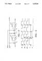
- FIG. 1is a circuit diagram of D-type flipflops shown an embodiment of the present invention.
- FIG. 2is a circuit diagram of the D-type flipflop shown in FIG. 1.
- FIG. 3is a timing diagram for explaining the operation of the circuit shown in FIG. 2.
- FIG. 4is a block diagram of the circuit shown in FIG. 1.
- FIG. 5is a timing diagram for explaining the operation of the circuit shown in FIG. 1.
- FIG. 6is a wiring block diagram of an application of the present invention to standard cells.
- FIG. 7is a circuit diagram showing an embodiment of an application of the present invention to a JK flipflop.
- FIG. 8is a block diagram of a simplified gate array.
- FIG. 9is a circuit diagram of a conventional D-type flipflop.
- FIG. 10is a timing diagram for explaining the operation of the circuit shown in FIG. 9.
- FIG. 11is a circuit diagram showing the circuit connection of conventional cascaded D-type flipflop.
- FIG. 12is a timing diagram for explaining the operation of the circuit shown in FIG. 11.
- 1is a PMOS transistor
- 2, 3, 6, 7are inverters
- 4 and 5are NMOS transistors.
- FIG. 2is a circuit diagram showing an improved D-type flipflop employed in one embodiment of the invention.
- the D-type flipflop shown in FIG. 2has a NMOS transistor 5 provided between the transistor 4 and the slave latch in comparison with the conventional flipflop shown in FIG. 9.
- the transistor 5operates in response to the signal CTI which indicates the holding in the next stage circuit connected to receive the output data signal Q.
- FIG. 3is a timing diagram for explaining the operation of the circuit shown in FIG. 2.
- the PMOS transistor 1is turned on in response to the fall of the clock signal CK
- the input data signal Dis held within the master latch formed by the inverters 2 and 3.
- the transistor 4is also turned on in response to the rise of the clock signal CK.
- a transistor 5is connected between the transistor 4 and the slave latch, the timing of the application of the data signal held in the master latch to the slave latch is controlled by the signal CTI. Therefore, the data signal held in the master latch is applied to the slave latch via transistors 4 and 5 in response to the rise of the signal CTI.
- FIG.is a circuit diagram of a cascaded D-type flipflop showing an embodiment of the invention.
- flipflops 10 and 20having the same circuit configuration of the D-type flipflop shown in FIG. 2 are cascaded.
- Flipflop 10is connected so as to receive the clock signal transmitted via the flipflop 20, i.e., to receive the signal CTO2 as the signal CTI1 via the wiring W3. This causes the transistor 5 in flipflop 10 to be turned on after data is held within the master latch in flipflop 20.
- the circuit connection of FIG. 1is shown as a block diagram in FIG. 4.
- the clock signal CKis provided to each flipflop 10 and 20 via the wiring W of FIG. 4, the clock signal CK2 provided to the flipflop 20 is delayed by ⁇ t with respect to the clock signal CK1 by clock skew. However, the signal CTO2 provided via the flipflop 20 is further delayed than the clock signal CK2. Since the clock signal CTI1 provided to the transistor 5 in flipflop 10 is simultaneous or delayed with respect to the signal CTO2, the rise of the data signal Q1, i.e., the output of the flipflop 10 is provided after the rise of the clock signal CK2.
- FIG. 6An embodiment of a standard cell employed in the present invention is shown in FIG. 6.
- standard cells 11-14 forming a D-type flipflopare cascaded by wiring W1, W2 and W3.
- Each wiring W1connects the input/output of each standard cell 11-14.
- the wiring W2provides the clock signals to each standard cell 11-14.
- Each wiring W3transmits the signal indicating the holding of the master latch in each later stage flipflop to each prior stage flipflop as signal CTI.
- a JK flipflopcomprises a D-type flipflop portion 8 and a logical gate portion 9.
- the logical gate portion 9includes a logical circuit necessary to form a JK flipflop.
- transmitting means for transmitting the data signal held in the first holding means to the second holding means in response to the holding of the second holding meansis provided to obtain a delay circuit which can reliably delay the applied data signal in response to the clock signal.
Landscapes
- Design And Manufacture Of Integrated Circuits (AREA)
Abstract
Description
This application is a continuation of Ser. No. 07/664,212, filed Mar. 4, 1991, now abandoned.
This application claims priority to Japanese Patent Application Serial No. 02-54785, filed Mar. 6, 1990,
inventor Akihiro Yanai.
1. Field of the Invention
The invention relates generally to delay circuits, and more particularly, to a delay circuit for delaying the supplied signal in response to the clock signal with high reliability.
2. Description of the Related Art
In the design of semi-customized LSI such as standard cells and gate arrays, computer aided design (hereinafter referred to as "CAD") is widely used. For example, a circuit block cell having standard features is previously prepared to be previously registered in a library under the standard cell method. With the CAD system, the desired circuit block cells are automatically arranged and wired in accordance with an automatic arrangement wiring program. In the execution of the automatic arrangement wiring program, the area for arrangement of the wiring is used as effectively as possible to minimize the occupying area of the circuit. As a result, it is seldom that the length of the wiring is designed to be minimum.
However, the delay caused by the wiring for connecting elements has recently evolved into a problem that cannot be ignored as the rapid operation of semiconductor integrated circuits advances. Under such a circumstance, the problem set forth hereinafter occurs when more than one master slave type flipflops are cascaded. In the following description, a delay type (hereinafter referred to as "D-type") flipflop is adopted as an example of a master slave type flipflop.
FIG. 8 is a simplified block diagram of a gate array. Referring to FIG. 8, the gate array comprises an input/output pad 30 for externally inputting/outputting signals, andbase cell columns
FIG. 9 is a circuit diagram of a conventional D-type flipflop. A D-type flipflop has the most simple circuit configuration among the numerous master slave type flipflops. Referring to FIG. 9, the D-type flipflop comprisesinverters inverters PMOS transistor 1 is connected for the purpose of input control of the master latch. For the output control of the master latch, a NMOS transistor 4 is connected.Transistors 1 and 4 operate in response to clock signal CK. Data D applied to the D-type flipflop is provided as the output data Q with a delay defined by the frequency of the clock signal CK.
FIG. 10 is a timing diagram for explaining the operation of the circuit shown in FIG. 9. In operation, input data D is sampled and held in the master latch formed byinverters inverters
FIG. 11 is a circuit diagram showing the circuit connection when two D-type flipflops are cascaded. FIG. 12 is a timing diagram for explaining the operation. It should be noted in FIG. 12 that the clock signal CK2 applied to theflipflop 92 is delayed by Δt with respect to the clock signal CK1 applied toflipflop 91 by clock skew. This delay time Δt may be caused by arranging and wiring the twoflipflops flipflop 92 is connected so as to receive the clock signal CK via a wiring W longer than theflipflop 91 to cause the delay time at called clock skew.
As shown in FIG. 12, theflipflop 91 establishes an output data signal Q1 in response to the fall and subsequent rise of the clock signal CK1. In the embodiment, a high level data signal Q1 is provided. When data signal Q1 rises, Q1 rises as a result of clock signal CK1 being raised, the clock signal CK2 is not yet raised because, the clock signal CK2 is delayed. This causes the raised high data signal Q1 to be sampled in theflipflop 92 clock signal CK2 rises after A1 rises. As a result, a high data signal Q1 from theflipflop 91 is provided as data signal Q2 from theflipflop 92 in response to the same rise of the clock signal CK. In other words, data D passes through twoflipflops type flipflops
The present invention is provided to solve the above-described problem with the object of reliably delaying the applied signal in response to the clock signal in the delay circuit.
The delay circuit in accordance with the present invention comprises first and second cascaded holding means each responsive to clock signals for holding applied data signals, signal line means for applying the clock signal provided to the first holding means to the second holding means with delay, and transmitting means for transmitting the data signal held in the first holding means to the second holding means in response to the holding of the second holding means.
In the delay circuit of the present invention, since the transmitting means supplies the data signal held in the first holding means to the second holding means in response to the holding of the second holding means, the passing through of the data signal is prevented even when the timing of the clock signal applied to each of the first and second holding means deviates from each other.
FIG. 1 is a circuit diagram of D-type flipflops shown an embodiment of the present invention.
FIG. 2 is a circuit diagram of the D-type flipflop shown in FIG. 1.
FIG. 3 is a timing diagram for explaining the operation of the circuit shown in FIG. 2.
FIG. 4 is a block diagram of the circuit shown in FIG. 1.
FIG. 5 is a timing diagram for explaining the operation of the circuit shown in FIG. 1.
FIG. 6 is a wiring block diagram of an application of the present invention to standard cells.
FIG. 7 is a circuit diagram showing an embodiment of an application of the present invention to a JK flipflop.
FIG. 8 is a block diagram of a simplified gate array.
FIG. 9 is a circuit diagram of a conventional D-type flipflop.
FIG. 10 is a timing diagram for explaining the operation of the circuit shown in FIG. 9.
FIG. 11 is a circuit diagram showing the circuit connection of conventional cascaded D-type flipflop.
FIG. 12 is a timing diagram for explaining the operation of the circuit shown in FIG. 11.
In the drawings, 1 is a PMOS transistor, 2, 3, 6, 7 are inverters, 4 and 5 are NMOS transistors.
FIG. 2 is a circuit diagram showing an improved D-type flipflop employed in one embodiment of the invention. The D-type flipflop shown in FIG. 2 has a NMOS transistor 5 provided between the transistor 4 and the slave latch in comparison with the conventional flipflop shown in FIG. 9. The transistor 5 operates in response to the signal CTI which indicates the holding in the next stage circuit connected to receive the output data signal Q.
FIG. 3 is a timing diagram for explaining the operation of the circuit shown in FIG. 2. In operation, since thePMOS transistor 1 is turned on in response to the fall of the clock signal CK, the input data signal D is held within the master latch formed by theinverters
FIG. is a circuit diagram of a cascaded D-type flipflop showing an embodiment of the invention. Referring to FIG. 1, flipflops 10 and 20 having the same circuit configuration of the D-type flipflop shown in FIG. 2 are cascaded.Flipflop 10 is connected so as to receive the clock signal transmitted via theflipflop 20, i.e., to receive the signal CTO2 as the signal CTI1 via the wiring W3. This causes the transistor 5 inflipflop 10 to be turned on after data is held within the master latch inflipflop 20. The circuit connection of FIG. 1 is shown as a block diagram in FIG. 4.
Referring to the timing diagram of FIG. 5, the operation of the circuit shown in FIG. will be explained. Since the clock signal CK is provided to eachflipflop flipflop 20 is delayed by Δt with respect to the clock signal CK1 by clock skew. However, the signal CTO2 provided via theflipflop 20 is further delayed than the clock signal CK2. Since the clock signal CTI1 provided to the transistor 5 inflipflop 10 is simultaneous or delayed with respect to the signal CTO2, the rise of the data signal Q1, i.e., the output of theflipflop 10 is provided after the rise of the clock signal CK2. In other words, after the previous data D2 is held within the master latch of theflipflop 20, the transistor 5 of theflipflop 10 is turned on to output the data signal Q1. Consequently, it is understood that the "passing through of data" phenomenon in conventional circuits described in conjunction with FIG. 12 may be reliably prevented.
An embodiment of a standard cell employed in the present invention is shown in FIG. 6. Referring to FIG. 6, standard cells 11-14 forming a D-type flipflop are cascaded by wiring W1, W2 and W3. Each wiring W1 connects the input/output of each standard cell 11-14. The wiring W2 provides the clock signals to each standard cell 11-14. Each wiring W3 transmits the signal indicating the holding of the master latch in each later stage flipflop to each prior stage flipflop as signal CTI.
The above description has been accomplished where the present invention is applied to D-type flipflop as an example. It is noted that a circuit having master slave-type flipflops cascaded is also applicable. For example, an application of the present invention to a JK flipflop is shown in FIG. 7. The JK flipflop comprises a D-type flipflop portion 8 and alogical gate portion 9. Thelogical gate portion 9 includes a logical circuit necessary to form a JK flipflop.
In accordance with the present invention, transmitting means for transmitting the data signal held in the first holding means to the second holding means in response to the holding of the second holding means is provided to obtain a delay circuit which can reliably delay the applied data signal in response to the clock signal.
Claims (14)
1. A synchronous circuit with a clock skew compensating function, said synchronous circuit comprising:
a master latch having a corresponding master data input and master data output;
a slave latch having a corresponding slave data input and slave data output;
first coupling means, responding to a first lock signal, for selectively applying a first data signal to the master data input of the master latch in synchronism with the first clock signal;
second coupling means, for coupling a master output signal developed at the master data output of the master latch to the slave data input of the slave latch;
third coupling means, coupled between the second coupling means and the slave latch responding to a second clock signal, for temporarily blocking the master output signal from reaching the slave data input;
a first wire for coupling a slave output signal developed at the slave data output to a subsequent circuit;
a second wire, receiving said first clock signal for introducing a time delay to the first clock signal thereby developing a delayed version of the first clock signal, said second wire providing the delayed version of the first clock signal to the subsequent circuit; and
a third wire for returning the delayed version of the first clock signal to the third coupling means as said second clock signal.
2. The synchronous circuit of claim 1 wherein the second coupling means includes switch means, responding to the first clock signal, for selectively passing the master output signal developed at the master data output of the master latch to the third coupling means in synchronism with the first clock signal.
3. The synchronous circuit of claim 1 or 2 where said subsequent circuit is a second synchronous circuit according to claim 1.
4. The synchronous circuit of claim 1 where said synchronous circuit and said subsequent circuit are defined on an integrated circuit.
5. The synchronous circuit of claim 1 where said synchronous circuit and a subsequent circuit are cascaded flip flops forming part of a shift register.
6. The synchronous circuit of claim 1 where said synchronous circuit further comprises:
logical gate circuitry receiving J and K inputs and the slave data output, said logical gate circuitry supplying the first data signal to the first coupling means to form a JK type flip flop.
7. The synchronous circuit of claim 1 where said synchronous circuit is a D type flip flop.
8. The synchronous circuit of claim 1 wherein:
the first coupling means includes a first transistor of a first conductivity type controlled by the first clock signal;
the second coupling means includes a second transistor of a second conductivity type controlled by the first clock signal; and
the third coupling means includes a third transistor of said second conductivity type controlled by the second clock signal.
9. The synchronous circuit of claim 8 wherein the first transistor is a PMOS transistor, the second transistor is a NMOS transistor, and the third transistor is a NMOS transistor.
10. The synchronous circuit of claim 8 wherein:
the master latch includes a first inverter having an input and an output, and a second inverter having an input and an output respectively coupled to the output and input of the first inverter; and
the slave latch includes a third inverter having an input and an output, an da fourth inverter having an input and an output respectively coupled to the output and input of the third inverter.
11. A synchronous system with a clock skew compensating function comprising:
a first synchronous circuit unit having a first data input node, a first clock input node, a time-delayed clock input node, and a first data output node, where the first synchronous circuit unit processes a first data signal presented at the first data input node when a first clock signal is received at the corresponding first clock input node;
a second synchronous circuit unit having a second data input node, a second clock input node, a second data output node, and a time-delayed clock output node, where the second synchronous circuit unit processes a second data signal presented at the second data input node when a second clock signal is received at the corresponding second clock input node and where the time-delayed clock output node outputs an indicating signal that indicates receipt of the second clock signal by the second synchronous circuit unit;
a first wire of predetermined length coupling the first data output node to the second data input node;
a second wire of predetermined length coupling the first clock input node to the second clock input node, the length of said second wire causing the second clock signal to be time-delayed relative to the first clock signal; and
a third wire coupling the time-delayed clock output node of the second synchronous circuit unit to the time-delayed clock input node of the first synchronous circuit unit;
wherein said first synchronous circuit unit includes output delay means, responsive to the indicating signal, for delaying production of an output signal at the first data output node until said output delay means receives the indicating signal.
12. A synchronous system according to claim 11 wherein the first synchronous circuit unit and the second synchronous circuit unit are defined in spaced-apart areas of an integrated circuit.
13. A synchronous system according to claim 11 wherein the first synchronous circuit unit and the second synchronous circuit unit define parts of spaced-apart or adjacent cells in a gate array integrated circuit.
14. A clock skew compensating method for a synchronous system having first and second circuit units connected in sequence where the second circuit unit receives a wire-length delayed clock signal after the first circuit unit receives a relatively non-delayed clock signal, and where the first circuit unit has a first circuit output connected to a second circuit input the second circuit unit, said method comprising the steps of:
generating an indicating signal that indicates receipt of the wire-length delayed clock signal by the second circuit unit;
transmitting the indicating signal to the first circuit unit; and
inhibiting the first circuit output from changing until the indicating signal is received by the first circuit unit.
Priority Applications (1)
| Application Number | Priority Date | Filing Date | Title |
|---|---|---|---|
| US07/914,053US5239206A (en) | 1990-03-06 | 1992-07-13 | Synchronous circuit with clock skew compensating function and circuits utilizing same |
Applications Claiming Priority (4)
| Application Number | Priority Date | Filing Date | Title |
|---|---|---|---|
| JP2-54785 | 1990-03-06 | ||
| JP2054785AJPH03257949A (en) | 1990-03-06 | 1990-03-06 | Delay circuit |
| US66421291A | 1991-03-04 | 1991-03-04 | |
| US07/914,053US5239206A (en) | 1990-03-06 | 1992-07-13 | Synchronous circuit with clock skew compensating function and circuits utilizing same |
Related Parent Applications (1)
| Application Number | Title | Priority Date | Filing Date |
|---|---|---|---|
| US66421291AContinuation | 1990-03-06 | 1991-03-04 |
Publications (1)
| Publication Number | Publication Date |
|---|---|
| US5239206Atrue US5239206A (en) | 1993-08-24 |
Family
ID=27295408
Family Applications (1)
| Application Number | Title | Priority Date | Filing Date |
|---|---|---|---|
| US07/914,053Expired - LifetimeUS5239206A (en) | 1990-03-06 | 1992-07-13 | Synchronous circuit with clock skew compensating function and circuits utilizing same |
Country Status (1)
| Country | Link |
|---|---|
| US (1) | US5239206A (en) |
Cited By (64)
| Publication number | Priority date | Publication date | Assignee | Title |
|---|---|---|---|---|
| US5287394A (en)* | 1993-03-22 | 1994-02-15 | Advanced Micro Devices, Inc. | Fast counter with uniform delay structures |
| US5414745A (en)* | 1993-06-01 | 1995-05-09 | Advanced Micro Devices, Inc. | Synchronized clocking disable and enable circuit |
| US5463338A (en)* | 1993-06-07 | 1995-10-31 | Vlsi Technology, Inc. | Dual latch clocked LSSD and method |
| US5497114A (en)* | 1993-12-22 | 1996-03-05 | Fujitsu Limited | Flip-flop circuit |
| US5508648A (en)* | 1994-08-01 | 1996-04-16 | Intel Corporation | Differential latch circuit |
| US5521953A (en)* | 1992-12-04 | 1996-05-28 | Texas Instruments Incorporated | Shift register with transfer gate-inverter arrangement providing stable operation |
| US5576643A (en)* | 1994-12-09 | 1996-11-19 | Fujitsu Limited | Data transfer circuit device |
| US5636165A (en)* | 1995-04-14 | 1997-06-03 | Martin Marietta Corporation | Apparatus for and method of facilitating proper data transfer between two or more digital memory elements |
| US5654659A (en)* | 1994-02-28 | 1997-08-05 | Nec Corporation | Scan circuit having a reduced clock signal delay |
| US5684422A (en)* | 1995-01-25 | 1997-11-04 | Advanced Micro Devices, Inc. | Pipelined microprocessor including a high speed single-clock latch circuit |
| US5699002A (en)* | 1995-01-19 | 1997-12-16 | Mitsubishi Denki Kabushiki Kaisha | Flip-flop circuit, and shift register circuit, serial-parallel converter and parallel-serial converter using the same |
| US5760624A (en)* | 1995-04-28 | 1998-06-02 | Altera Corporation | Power-on reset circuit with hysteresis |
| US5831462A (en)* | 1995-03-08 | 1998-11-03 | Advanced Micro Devices, Inc. | Conditional latching mechanism and pipelined microprocessor employing the same |
| US5838177A (en)* | 1997-01-06 | 1998-11-17 | Micron Technology, Inc. | Adjustable output driver circuit having parallel pull-up and pull-down elements |
| US5852378A (en)* | 1997-02-11 | 1998-12-22 | Micron Technology, Inc. | Low-skew differential signal converter |
| US5870347A (en)* | 1997-03-11 | 1999-02-09 | Micron Technology, Inc. | Multi-bank memory input/output line selection |
| US5872736A (en)* | 1996-10-28 | 1999-02-16 | Micron Technology, Inc. | High speed input buffer |
| US5874843A (en)* | 1997-05-28 | 1999-02-23 | Taiwan Semiconductor Manufacturing Co., Ltd. | Power-on reset circuit without an RC Network |
| US5917758A (en)* | 1996-11-04 | 1999-06-29 | Micron Technology, Inc. | Adjustable output driver circuit |
| US5920518A (en)* | 1997-02-11 | 1999-07-06 | Micron Technology, Inc. | Synchronous clock generator including delay-locked loop |
| US5923594A (en)* | 1998-02-17 | 1999-07-13 | Micron Technology, Inc. | Method and apparatus for coupling data from a memory device using a single ended read data path |
| US5926047A (en)* | 1997-08-29 | 1999-07-20 | Micron Technology, Inc. | Synchronous clock generator including a delay-locked loop signal loss detector |
| US5940608A (en)* | 1997-02-11 | 1999-08-17 | Micron Technology, Inc. | Method and apparatus for generating an internal clock signal that is synchronized to an external clock signal |
| US5946244A (en)* | 1997-03-05 | 1999-08-31 | Micron Technology, Inc. | Delay-locked loop with binary-coupled capacitor |
| US5949254A (en)* | 1996-11-26 | 1999-09-07 | Micron Technology, Inc. | Adjustable output driver circuit |
| US5953284A (en)* | 1997-07-09 | 1999-09-14 | Micron Technology, Inc. | Method and apparatus for adaptively adjusting the timing of a clock signal used to latch digital signals, and memory device using same |
| US5956502A (en)* | 1997-03-05 | 1999-09-21 | Micron Technology, Inc. | Method and circuit for producing high-speed counts |
| US6011732A (en)* | 1997-08-20 | 2000-01-04 | Micron Technology, Inc. | Synchronous clock generator including a compound delay-locked loop |
| US6014759A (en)* | 1997-06-13 | 2000-01-11 | Micron Technology, Inc. | Method and apparatus for transferring test data from a memory array |
| US6016282A (en)* | 1998-05-28 | 2000-01-18 | Micron Technology, Inc. | Clock vernier adjustment |
| US6029250A (en)* | 1998-09-09 | 2000-02-22 | Micron Technology, Inc. | Method and apparatus for adaptively adjusting the timing offset between a clock signal and digital signals transmitted coincident with that clock signal, and memory device and system using same |
| US6044429A (en)* | 1997-07-10 | 2000-03-28 | Micron Technology, Inc. | Method and apparatus for collision-free data transfers in a memory device with selectable data or address paths |
| US6058156A (en)* | 1997-05-29 | 2000-05-02 | Nec Corporation | Shift register device and method of driving the same |
| US6101197A (en)* | 1997-09-18 | 2000-08-08 | Micron Technology, Inc. | Method and apparatus for adjusting the timing of signals over fine and coarse ranges |
| US6105106A (en)* | 1997-12-31 | 2000-08-15 | Micron Technology, Inc. | Computer system, memory device and shift register including a balanced switching circuit with series connected transfer gates which are selectively clocked for fast switching times |
| US6115318A (en)* | 1996-12-03 | 2000-09-05 | Micron Technology, Inc. | Clock vernier adjustment |
| US6173432B1 (en) | 1997-06-20 | 2001-01-09 | Micron Technology, Inc. | Method and apparatus for generating a sequence of clock signals |
| US6212482B1 (en) | 1998-03-06 | 2001-04-03 | Micron Technology, Inc. | Circuit and method for specifying performance parameters in integrated circuits |
| US6218878B1 (en)* | 1997-01-25 | 2001-04-17 | Nippon Precision Circuits, Inc. | D-type flip-flop circiut |
| US6256234B1 (en) | 1997-02-11 | 2001-07-03 | Micron Technology, Inc. | Low skew differential receiver with disable feature |
| US6269451B1 (en) | 1998-02-27 | 2001-07-31 | Micron Technology, Inc. | Method and apparatus for adjusting data timing by delaying clock signal |
| US6279090B1 (en) | 1998-09-03 | 2001-08-21 | Micron Technology, Inc. | Method and apparatus for resynchronizing a plurality of clock signals used in latching respective digital signals applied to a packetized memory device |
| US6338127B1 (en) | 1998-08-28 | 2002-01-08 | Micron Technology, Inc. | Method and apparatus for resynchronizing a plurality of clock signals used to latch respective digital signals, and memory device using same |
| US6349399B1 (en) | 1998-09-03 | 2002-02-19 | Micron Technology, Inc. | Method and apparatus for generating expect data from a captured bit pattern, and memory device using same |
| US6374360B1 (en) | 1998-12-11 | 2002-04-16 | Micron Technology, Inc. | Method and apparatus for bit-to-bit timing correction of a high speed memory bus |
| US6405280B1 (en) | 1998-06-05 | 2002-06-11 | Micron Technology, Inc. | Packet-oriented synchronous DRAM interface supporting a plurality of orderings for data block transfers within a burst sequence |
| US6430696B1 (en) | 1998-11-30 | 2002-08-06 | Micron Technology, Inc. | Method and apparatus for high speed data capture utilizing bit-to-bit timing correction, and memory device using same |
| US6509772B1 (en)* | 2000-10-23 | 2003-01-21 | Intel Corporation | Flip-flop circuit with transmission-gate sampling |
| US6559700B2 (en)* | 2000-11-07 | 2003-05-06 | Sharp Kabushiki Kaisha | Semiconductor integrated circuit |
| US6567338B1 (en) | 1996-04-19 | 2003-05-20 | Integrated Device Technology, Inc. | Fully synchronous pipelined RAM |
| US6591354B1 (en) | 1998-02-23 | 2003-07-08 | Integrated Device Technology, Inc. | Separate byte control on fully synchronous pipelined SRAM |
| US6597225B1 (en)* | 2002-03-22 | 2003-07-22 | Agere Systems Inc. | Data capture circuit with series channel sampling structure |
| US6720815B2 (en)* | 1998-11-10 | 2004-04-13 | Renesas Technology Corp. | Phase adjustor for semiconductor integrated circuit |
| US20040085109A1 (en)* | 2002-11-05 | 2004-05-06 | Ip-First Llc | Method and apparatus for fine tuning clock signals of an integrated circuit |
| US20040113668A1 (en)* | 2002-12-13 | 2004-06-17 | Ip-First Llc | Integrated circuit timing debug apparatus and method |
| US6801989B2 (en) | 2001-06-28 | 2004-10-05 | Micron Technology, Inc. | Method and system for adjusting the timing offset between a clock signal and respective digital signals transmitted along with that clock signal, and memory device and computer system using same |
| US6912680B1 (en) | 1997-02-11 | 2005-06-28 | Micron Technology, Inc. | Memory system with dynamic timing correction |
| US6931086B2 (en) | 1999-03-01 | 2005-08-16 | Micron Technology, Inc. | Method and apparatus for generating a phase dependent control signal |
| US20060119371A1 (en)* | 2004-11-10 | 2006-06-08 | Elpida Memory, Inc | Semiconductor device and evaluation circuit for the same |
| US7069406B2 (en) | 1999-07-02 | 2006-06-27 | Integrated Device Technology, Inc. | Double data rate synchronous SRAM with 100% bus utilization |
| US7168027B2 (en) | 2003-06-12 | 2007-01-23 | Micron Technology, Inc. | Dynamic synchronization of data capture on an optical or other high speed communications link |
| US7234070B2 (en) | 2003-10-27 | 2007-06-19 | Micron Technology, Inc. | System and method for using a learning sequence to establish communications on a high-speed nonsynchronous interface in the absence of clock forwarding |
| WO2014179944A1 (en)* | 2013-05-08 | 2014-11-13 | Qualcomm Incorporated | Flip-flop for reducing dynamic power |
| US20170040068A1 (en)* | 2015-08-05 | 2017-02-09 | Shenzhen China Star Optoelectronics Technology Co. Ltd. | Driving circuits and the shift register circuits |
Citations (19)
| Publication number | Priority date | Publication date | Assignee | Title |
|---|---|---|---|---|
| US3588527A (en)* | 1969-04-04 | 1971-06-28 | Westinghouse Electric Corp | Shift register using complementary induced channel field effect semiconductor devices |
| US3812384A (en)* | 1973-05-17 | 1974-05-21 | Rca Corp | Set-reset flip-flop |
| US4103185A (en)* | 1976-03-04 | 1978-07-25 | Rca Corporation | Memory cells |
| US4275316A (en)* | 1978-11-06 | 1981-06-23 | Rca Corporation | Resettable bistable circuit |
| US4495629A (en)* | 1983-01-25 | 1985-01-22 | Storage Technology Partners | CMOS scannable latch |
| US4554467A (en)* | 1983-06-22 | 1985-11-19 | Motorola, Inc. | CMOS Flip-flop |
| US4667339A (en)* | 1983-12-05 | 1987-05-19 | Texas Instruments Incorporated | Level sensitive latch stage |
| US4691122A (en)* | 1985-03-29 | 1987-09-01 | Advanced Micro Devices, Inc. | CMOS D-type flip-flop circuits |
| JPS62260421A (en)* | 1986-05-06 | 1987-11-12 | Matsushita Electric Ind Co Ltd | Complementary D-type flip-flop circuit |
| JPS6316710A (en)* | 1986-07-09 | 1988-01-23 | Nec Corp | Latch circuit |
| US4733405A (en)* | 1985-10-15 | 1988-03-22 | Sony Corporation | Digital integrated circuit |
| JPS6367011A (en)* | 1986-09-08 | 1988-03-25 | Sharp Corp | Set/reset flip-flop circuit |
| JPS63209212A (en)* | 1987-02-25 | 1988-08-30 | Hitachi Ltd | latch driver circuit |
| JPS644016A (en)* | 1987-06-25 | 1989-01-09 | Mitsubishi Electric Corp | Furnace tube |
| JPS6458817A (en)* | 1987-08-28 | 1989-03-06 | K Seven Kk | Clutch |
| US4843254A (en)* | 1987-03-02 | 1989-06-27 | Oki Electric Industry Co., Ltd. | Master-slave flip-flop circuit with three phase clocking |
| US4974241A (en)* | 1989-03-31 | 1990-11-27 | Sgs-Thomson Microelectronics, Inc. | Counter employing exclusive NOR gate and latches in combination |
| US5015875A (en)* | 1989-12-01 | 1991-05-14 | Motorola, Inc. | Toggle-free scan flip-flop |
| US5118975A (en)* | 1990-03-05 | 1992-06-02 | Thinking Machines Corporation | Digital clock buffer circuit providing controllable delay |
- 1992
- 1992-07-13USUS07/914,053patent/US5239206A/ennot_activeExpired - Lifetime
Patent Citations (19)
| Publication number | Priority date | Publication date | Assignee | Title |
|---|---|---|---|---|
| US3588527A (en)* | 1969-04-04 | 1971-06-28 | Westinghouse Electric Corp | Shift register using complementary induced channel field effect semiconductor devices |
| US3812384A (en)* | 1973-05-17 | 1974-05-21 | Rca Corp | Set-reset flip-flop |
| US4103185A (en)* | 1976-03-04 | 1978-07-25 | Rca Corporation | Memory cells |
| US4275316A (en)* | 1978-11-06 | 1981-06-23 | Rca Corporation | Resettable bistable circuit |
| US4495629A (en)* | 1983-01-25 | 1985-01-22 | Storage Technology Partners | CMOS scannable latch |
| US4554467A (en)* | 1983-06-22 | 1985-11-19 | Motorola, Inc. | CMOS Flip-flop |
| US4667339A (en)* | 1983-12-05 | 1987-05-19 | Texas Instruments Incorporated | Level sensitive latch stage |
| US4691122A (en)* | 1985-03-29 | 1987-09-01 | Advanced Micro Devices, Inc. | CMOS D-type flip-flop circuits |
| US4733405A (en)* | 1985-10-15 | 1988-03-22 | Sony Corporation | Digital integrated circuit |
| JPS62260421A (en)* | 1986-05-06 | 1987-11-12 | Matsushita Electric Ind Co Ltd | Complementary D-type flip-flop circuit |
| JPS6316710A (en)* | 1986-07-09 | 1988-01-23 | Nec Corp | Latch circuit |
| JPS6367011A (en)* | 1986-09-08 | 1988-03-25 | Sharp Corp | Set/reset flip-flop circuit |
| JPS63209212A (en)* | 1987-02-25 | 1988-08-30 | Hitachi Ltd | latch driver circuit |
| US4843254A (en)* | 1987-03-02 | 1989-06-27 | Oki Electric Industry Co., Ltd. | Master-slave flip-flop circuit with three phase clocking |
| JPS644016A (en)* | 1987-06-25 | 1989-01-09 | Mitsubishi Electric Corp | Furnace tube |
| JPS6458817A (en)* | 1987-08-28 | 1989-03-06 | K Seven Kk | Clutch |
| US4974241A (en)* | 1989-03-31 | 1990-11-27 | Sgs-Thomson Microelectronics, Inc. | Counter employing exclusive NOR gate and latches in combination |
| US5015875A (en)* | 1989-12-01 | 1991-05-14 | Motorola, Inc. | Toggle-free scan flip-flop |
| US5118975A (en)* | 1990-03-05 | 1992-06-02 | Thinking Machines Corporation | Digital clock buffer circuit providing controllable delay |
Cited By (129)
| Publication number | Priority date | Publication date | Assignee | Title |
|---|---|---|---|---|
| US5521953A (en)* | 1992-12-04 | 1996-05-28 | Texas Instruments Incorporated | Shift register with transfer gate-inverter arrangement providing stable operation |
| US5287394A (en)* | 1993-03-22 | 1994-02-15 | Advanced Micro Devices, Inc. | Fast counter with uniform delay structures |
| US5414745A (en)* | 1993-06-01 | 1995-05-09 | Advanced Micro Devices, Inc. | Synchronized clocking disable and enable circuit |
| US5463338A (en)* | 1993-06-07 | 1995-10-31 | Vlsi Technology, Inc. | Dual latch clocked LSSD and method |
| US5497114A (en)* | 1993-12-22 | 1996-03-05 | Fujitsu Limited | Flip-flop circuit |
| US5654659A (en)* | 1994-02-28 | 1997-08-05 | Nec Corporation | Scan circuit having a reduced clock signal delay |
| US5508648A (en)* | 1994-08-01 | 1996-04-16 | Intel Corporation | Differential latch circuit |
| US5576643A (en)* | 1994-12-09 | 1996-11-19 | Fujitsu Limited | Data transfer circuit device |
| US5699002A (en)* | 1995-01-19 | 1997-12-16 | Mitsubishi Denki Kabushiki Kaisha | Flip-flop circuit, and shift register circuit, serial-parallel converter and parallel-serial converter using the same |
| US5684422A (en)* | 1995-01-25 | 1997-11-04 | Advanced Micro Devices, Inc. | Pipelined microprocessor including a high speed single-clock latch circuit |
| US5831462A (en)* | 1995-03-08 | 1998-11-03 | Advanced Micro Devices, Inc. | Conditional latching mechanism and pipelined microprocessor employing the same |
| US5636165A (en)* | 1995-04-14 | 1997-06-03 | Martin Marietta Corporation | Apparatus for and method of facilitating proper data transfer between two or more digital memory elements |
| US5760624A (en)* | 1995-04-28 | 1998-06-02 | Altera Corporation | Power-on reset circuit with hysteresis |
| US6567338B1 (en) | 1996-04-19 | 2003-05-20 | Integrated Device Technology, Inc. | Fully synchronous pipelined RAM |
| US6785188B2 (en) | 1996-04-19 | 2004-08-31 | Integrated Device Technology, Inc. | Fully synchronous pipelined RAM |
| US5872736A (en)* | 1996-10-28 | 1999-02-16 | Micron Technology, Inc. | High speed input buffer |
| US5910920A (en)* | 1996-10-28 | 1999-06-08 | Micron Technology, Inc. | High speed input buffer |
| US6437600B1 (en) | 1996-11-04 | 2002-08-20 | Micron Technology, Inc. | Adjustable output driver circuit |
| US5917758A (en)* | 1996-11-04 | 1999-06-29 | Micron Technology, Inc. | Adjustable output driver circuit |
| US6326810B1 (en) | 1996-11-04 | 2001-12-04 | Micron Technology, Inc. | Adjustable output driver circuit |
| US6084434A (en)* | 1996-11-26 | 2000-07-04 | Micron Technology, Inc. | Adjustable output driver circuit |
| US5949254A (en)* | 1996-11-26 | 1999-09-07 | Micron Technology, Inc. | Adjustable output driver circuit |
| US6115318A (en)* | 1996-12-03 | 2000-09-05 | Micron Technology, Inc. | Clock vernier adjustment |
| US5838177A (en)* | 1997-01-06 | 1998-11-17 | Micron Technology, Inc. | Adjustable output driver circuit having parallel pull-up and pull-down elements |
| US6069504A (en)* | 1997-01-06 | 2000-05-30 | Micron Technnology, Inc. | Adjustable output driver circuit having parallel pull-up and pull-down elements |
| US6218878B1 (en)* | 1997-01-25 | 2001-04-17 | Nippon Precision Circuits, Inc. | D-type flip-flop circiut |
| US5920518A (en)* | 1997-02-11 | 1999-07-06 | Micron Technology, Inc. | Synchronous clock generator including delay-locked loop |
| US6256234B1 (en) | 1997-02-11 | 2001-07-03 | Micron Technology, Inc. | Low skew differential receiver with disable feature |
| US6912680B1 (en) | 1997-02-11 | 2005-06-28 | Micron Technology, Inc. | Memory system with dynamic timing correction |
| US5852378A (en)* | 1997-02-11 | 1998-12-22 | Micron Technology, Inc. | Low-skew differential signal converter |
| US6069510A (en)* | 1997-02-11 | 2000-05-30 | Micron Technology, Inc. | Low-skew differential signal converter |
| US6340904B1 (en) | 1997-02-11 | 2002-01-22 | Micron Technology, Inc. | Method and apparatus for generating an internal clock signal that is synchronized to an external clock signal |
| US5940608A (en)* | 1997-02-11 | 1999-08-17 | Micron Technology, Inc. | Method and apparatus for generating an internal clock signal that is synchronized to an external clock signal |
| US6483757B2 (en) | 1997-03-05 | 2002-11-19 | Micron Technology, Inc. | Delay-locked loop with binary-coupled capacitor |
| US6262921B1 (en) | 1997-03-05 | 2001-07-17 | Micron Technology, Inc. | Delay-locked loop with binary-coupled capacitor |
| US5946244A (en)* | 1997-03-05 | 1999-08-31 | Micron Technology, Inc. | Delay-locked loop with binary-coupled capacitor |
| US5956502A (en)* | 1997-03-05 | 1999-09-21 | Micron Technology, Inc. | Method and circuit for producing high-speed counts |
| US6400641B1 (en) | 1997-03-05 | 2002-06-04 | Micron Technology, Inc. | Delay-locked loop with binary-coupled capacitor |
| US6490224B2 (en) | 1997-03-05 | 2002-12-03 | Micron Technology, Inc. | Delay-locked loop with binary-coupled capacitor |
| US6256259B1 (en) | 1997-03-05 | 2001-07-03 | Micron Technology, Inc. | Delay-locked loop with binary-coupled capacitor |
| US6490207B2 (en) | 1997-03-05 | 2002-12-03 | Micron Technology, Inc. | Delay-locked loop with binary-coupled capacitor |
| US5870347A (en)* | 1997-03-11 | 1999-02-09 | Micron Technology, Inc. | Multi-bank memory input/output line selection |
| US6256255B1 (en) | 1997-03-11 | 2001-07-03 | Micron Technology, Inc. | Multi-bank memory input/output line selection |
| US6122217A (en)* | 1997-03-11 | 2000-09-19 | Micron Technology, Inc. | Multi-bank memory input/output line selection |
| US5874843A (en)* | 1997-05-28 | 1999-02-23 | Taiwan Semiconductor Manufacturing Co., Ltd. | Power-on reset circuit without an RC Network |
| US6058156A (en)* | 1997-05-29 | 2000-05-02 | Nec Corporation | Shift register device and method of driving the same |
| US6519719B1 (en) | 1997-06-13 | 2003-02-11 | Micron Technology, Inc. | Method and apparatus for transferring test data from a memory array |
| US6014759A (en)* | 1997-06-13 | 2000-01-11 | Micron Technology, Inc. | Method and apparatus for transferring test data from a memory array |
| US6954097B2 (en) | 1997-06-20 | 2005-10-11 | Micron Technology, Inc. | Method and apparatus for generating a sequence of clock signals |
| US6173432B1 (en) | 1997-06-20 | 2001-01-09 | Micron Technology, Inc. | Method and apparatus for generating a sequence of clock signals |
| US7889593B2 (en) | 1997-06-20 | 2011-02-15 | Round Rock Research, Llc | Method and apparatus for generating a sequence of clock signals |
| US7415404B2 (en) | 1997-06-20 | 2008-08-19 | Micron Technology, Inc. | Method and apparatus for generating a sequence of clock signals |
| US20110122710A1 (en)* | 1997-06-20 | 2011-05-26 | Round Rock Research, Llc | Method and apparatus for generating a sequence of clock signals |
| US8565008B2 (en) | 1997-06-20 | 2013-10-22 | Round Rock Research, Llc | Method and apparatus for generating a sequence of clock signals |
| US5953284A (en)* | 1997-07-09 | 1999-09-14 | Micron Technology, Inc. | Method and apparatus for adaptively adjusting the timing of a clock signal used to latch digital signals, and memory device using same |
| US6026050A (en)* | 1997-07-09 | 2000-02-15 | Micron Technology, Inc. | Method and apparatus for adaptively adjusting the timing of a clock signal used to latch digital signals, and memory device using same |
| US6614698B2 (en) | 1997-07-10 | 2003-09-02 | Micron Technology, Inc. | Method and apparatus for synchronous data transfers in a memory device with selectable data or address paths |
| US6789175B2 (en) | 1997-07-10 | 2004-09-07 | Micron Technology, Inc. | Method and apparatus for synchronous data transfers in a memory device with selectable data or address paths |
| US6272608B1 (en) | 1997-07-10 | 2001-08-07 | Micron Technology, Inc. | Method and apparatus for synchronous data transfers in a memory device with lookahead logic for detecting latency intervals |
| US6044429A (en)* | 1997-07-10 | 2000-03-28 | Micron Technology, Inc. | Method and apparatus for collision-free data transfers in a memory device with selectable data or address paths |
| US6560668B2 (en) | 1997-07-10 | 2003-05-06 | Micron Technology, Inc. | Method and apparatus for reading write-modified read data in memory device providing synchronous data transfers |
| US6611885B2 (en) | 1997-07-10 | 2003-08-26 | Micron Technology, Inc. | Method and apparatus for synchronous data transfers in a memory device with selectable data or address paths |
| US6415340B1 (en) | 1997-07-10 | 2002-07-02 | Micron Technology, Inc. | Method and apparatus for synchronous data transfers in a memory device with selectable data or address paths |
| US6556483B2 (en) | 1997-07-10 | 2003-04-29 | Micron Technology, Inc. | Method and apparatus for synchronous data transfers in a memory device with selectable data or address paths |
| US6011732A (en)* | 1997-08-20 | 2000-01-04 | Micron Technology, Inc. | Synchronous clock generator including a compound delay-locked loop |
| US5926047A (en)* | 1997-08-29 | 1999-07-20 | Micron Technology, Inc. | Synchronous clock generator including a delay-locked loop signal loss detector |
| US6201424B1 (en) | 1997-08-29 | 2001-03-13 | Micron Technology, Inc. | Synchronous clock generator including a delay-locked loop signal loss detector |
| US6101197A (en)* | 1997-09-18 | 2000-08-08 | Micron Technology, Inc. | Method and apparatus for adjusting the timing of signals over fine and coarse ranges |
| US6959016B1 (en) | 1997-09-18 | 2005-10-25 | Micron Technology, Inc. | Method and apparatus for adjusting the timing of signals over fine and coarse ranges |
| US6522163B1 (en) | 1997-12-31 | 2003-02-18 | Micron Technology, Inc. | Apparatus and method for coupling a first node to a second node using switches which are selectively clocked for fast switching times |
| US6516382B2 (en) | 1997-12-31 | 2003-02-04 | Micron Technology, Inc. | Memory device balanced switching circuit and method of controlling an array of transfer gates for fast switching times |
| US6105106A (en)* | 1997-12-31 | 2000-08-15 | Micron Technology, Inc. | Computer system, memory device and shift register including a balanced switching circuit with series connected transfer gates which are selectively clocked for fast switching times |
| US5923594A (en)* | 1998-02-17 | 1999-07-13 | Micron Technology, Inc. | Method and apparatus for coupling data from a memory device using a single ended read data path |
| US6091646A (en)* | 1998-02-17 | 2000-07-18 | Micron Technology, Inc. | Method and apparatus for coupling data from a memory device using a single ended read data path |
| US6591354B1 (en) | 1998-02-23 | 2003-07-08 | Integrated Device Technology, Inc. | Separate byte control on fully synchronous pipelined SRAM |
| US6499111B2 (en) | 1998-02-27 | 2002-12-24 | Micron Technology, Inc. | Apparatus for adjusting delay of a clock signal relative to a data signal |
| US6269451B1 (en) | 1998-02-27 | 2001-07-31 | Micron Technology, Inc. | Method and apparatus for adjusting data timing by delaying clock signal |
| US6327196B1 (en) | 1998-02-27 | 2001-12-04 | Micron Technology, Inc. | Synchronous memory device having an adjustable data clocking circuit |
| US6643789B2 (en) | 1998-02-27 | 2003-11-04 | Micron Technology, Inc. | Computer system having memory device with adjustable data clocking using pass gates |
| US6378079B1 (en) | 1998-02-27 | 2002-04-23 | Micron Technology, Inc. | Computer system having memory device with adjustable data clocking |
| US6212482B1 (en) | 1998-03-06 | 2001-04-03 | Micron Technology, Inc. | Circuit and method for specifying performance parameters in integrated circuits |
| US6393378B2 (en) | 1998-03-06 | 2002-05-21 | Micron Technology, Inc. | Circuit and method for specifying performance parameters in integrated circuits |
| US6016282A (en)* | 1998-05-28 | 2000-01-18 | Micron Technology, Inc. | Clock vernier adjustment |
| US6405280B1 (en) | 1998-06-05 | 2002-06-11 | Micron Technology, Inc. | Packet-oriented synchronous DRAM interface supporting a plurality of orderings for data block transfers within a burst sequence |
| US6338127B1 (en) | 1998-08-28 | 2002-01-08 | Micron Technology, Inc. | Method and apparatus for resynchronizing a plurality of clock signals used to latch respective digital signals, and memory device using same |
| US6477675B2 (en) | 1998-09-03 | 2002-11-05 | Micron Technology, Inc. | Method and apparatus for generating expect data from a captured bit pattern, and memory device using same |
| US6647523B2 (en) | 1998-09-03 | 2003-11-11 | Micron Technology, Inc. | Method for generating expect data from a captured bit pattern, and memory device using same |
| US7954031B2 (en) | 1998-09-03 | 2011-05-31 | Round Rock Research, Llc | Method and apparatus for generating expect data from a captured bit pattern, and memory device using same |
| US6279090B1 (en) | 1998-09-03 | 2001-08-21 | Micron Technology, Inc. | Method and apparatus for resynchronizing a plurality of clock signals used in latching respective digital signals applied to a packetized memory device |
| US7657813B2 (en) | 1998-09-03 | 2010-02-02 | Micron Technology, Inc. | Method and apparatus for generating expect data from a captured bit pattern, and memory device using same |
| US6349399B1 (en) | 1998-09-03 | 2002-02-19 | Micron Technology, Inc. | Method and apparatus for generating expect data from a captured bit pattern, and memory device using same |
| US7373575B2 (en) | 1998-09-03 | 2008-05-13 | Micron Technology, Inc. | Method and apparatus for generating expect data from a captured bit pattern, and memory device using same |
| US7085975B2 (en) | 1998-09-03 | 2006-08-01 | Micron Technology, Inc. | Method and apparatus for generating expect data from a captured bit pattern, and memory device using same |
| US6029250A (en)* | 1998-09-09 | 2000-02-22 | Micron Technology, Inc. | Method and apparatus for adaptively adjusting the timing offset between a clock signal and digital signals transmitted coincident with that clock signal, and memory device and system using same |
| US7084690B2 (en) | 1998-11-10 | 2006-08-01 | Renesas Technology Corp. | Semiconductor integrated circuit device |
| US6906572B2 (en) | 1998-11-10 | 2005-06-14 | Renesas Technology Corp. | Semiconductor integrated circuit device |
| US20050075855A1 (en)* | 1998-11-10 | 2005-04-07 | Hiroyuki Mizuno | Semiconductor integrated circuit device |
| US20040169535A1 (en)* | 1998-11-10 | 2004-09-02 | Hiroyuki Mizuno | Semiconductor integrated circuit device |
| US6720815B2 (en)* | 1998-11-10 | 2004-04-13 | Renesas Technology Corp. | Phase adjustor for semiconductor integrated circuit |
| US6430696B1 (en) | 1998-11-30 | 2002-08-06 | Micron Technology, Inc. | Method and apparatus for high speed data capture utilizing bit-to-bit timing correction, and memory device using same |
| US6662304B2 (en) | 1998-12-11 | 2003-12-09 | Micron Technology, Inc. | Method and apparatus for bit-to-bit timing correction of a high speed memory bus |
| US6374360B1 (en) | 1998-12-11 | 2002-04-16 | Micron Technology, Inc. | Method and apparatus for bit-to-bit timing correction of a high speed memory bus |
| US6931086B2 (en) | 1999-03-01 | 2005-08-16 | Micron Technology, Inc. | Method and apparatus for generating a phase dependent control signal |
| US7016451B2 (en) | 1999-03-01 | 2006-03-21 | Micron Technology, Inc. | Method and apparatus for generating a phase dependent control signal |
| US8433023B2 (en) | 1999-03-01 | 2013-04-30 | Round Rock Research, Llc | Method and apparatus for generating a phase dependent control signal |
| US8107580B2 (en) | 1999-03-01 | 2012-01-31 | Round Rock Research, Llc | Method and apparatus for generating a phase dependent control signal |
| US6952462B2 (en) | 1999-03-01 | 2005-10-04 | Micron Technology, Inc. | Method and apparatus for generating a phase dependent control signal |
| US7602876B2 (en) | 1999-03-01 | 2009-10-13 | Micron Technology, Inc. | Method and apparatus for generating a phase dependent control signal |
| US7418071B2 (en) | 1999-03-01 | 2008-08-26 | Micron Technology, Inc. | Method and apparatus for generating a phase dependent control signal |
| US7069406B2 (en) | 1999-07-02 | 2006-06-27 | Integrated Device Technology, Inc. | Double data rate synchronous SRAM with 100% bus utilization |
| US6509772B1 (en)* | 2000-10-23 | 2003-01-21 | Intel Corporation | Flip-flop circuit with transmission-gate sampling |
| US6559700B2 (en)* | 2000-11-07 | 2003-05-06 | Sharp Kabushiki Kaisha | Semiconductor integrated circuit |
| US7159092B2 (en) | 2001-06-28 | 2007-01-02 | Micron Technology, Inc. | Method and system for adjusting the timing offset between a clock signal and respective digital signals transmitted along with that clock signal, and memory device and computer system using same |
| US6801989B2 (en) | 2001-06-28 | 2004-10-05 | Micron Technology, Inc. | Method and system for adjusting the timing offset between a clock signal and respective digital signals transmitted along with that clock signal, and memory device and computer system using same |
| US6597225B1 (en)* | 2002-03-22 | 2003-07-22 | Agere Systems Inc. | Data capture circuit with series channel sampling structure |
| US7124314B2 (en) | 2002-11-05 | 2006-10-17 | Ip-First, Llc | Method and apparatus for fine tuning clock signals of an integrated circuit |
| US20040085109A1 (en)* | 2002-11-05 | 2004-05-06 | Ip-First Llc | Method and apparatus for fine tuning clock signals of an integrated circuit |
| US6903582B2 (en) | 2002-12-13 | 2005-06-07 | Ip First, Llc | Integrated circuit timing debug apparatus and method |
| US20040113668A1 (en)* | 2002-12-13 | 2004-06-17 | Ip-First Llc | Integrated circuit timing debug apparatus and method |
| US8892974B2 (en) | 2003-06-12 | 2014-11-18 | Round Rock Research, Llc | Dynamic synchronization of data capture on an optical or other high speed communications link |
| US7168027B2 (en) | 2003-06-12 | 2007-01-23 | Micron Technology, Inc. | Dynamic synchronization of data capture on an optical or other high speed communications link |
| US8181092B2 (en) | 2003-06-12 | 2012-05-15 | Round Rock Research, Llc | Dynamic synchronization of data capture on an optical or other high speed communications link |
| US7234070B2 (en) | 2003-10-27 | 2007-06-19 | Micron Technology, Inc. | System and method for using a learning sequence to establish communications on a high-speed nonsynchronous interface in the absence of clock forwarding |
| US7461286B2 (en) | 2003-10-27 | 2008-12-02 | Micron Technology, Inc. | System and method for using a learning sequence to establish communications on a high-speed nonsynchronous interface in the absence of clock forwarding |
| US20060119371A1 (en)* | 2004-11-10 | 2006-06-08 | Elpida Memory, Inc | Semiconductor device and evaluation circuit for the same |
| WO2014179944A1 (en)* | 2013-05-08 | 2014-11-13 | Qualcomm Incorporated | Flip-flop for reducing dynamic power |
| US9742382B2 (en) | 2013-05-08 | 2017-08-22 | Qualcomm Incorporated | Flip-flop for reducing dynamic power |
| US20170040068A1 (en)* | 2015-08-05 | 2017-02-09 | Shenzhen China Star Optoelectronics Technology Co. Ltd. | Driving circuits and the shift register circuits |
| US9672936B2 (en)* | 2015-08-05 | 2017-06-06 | Shenzhen China Star Optoelectronics Technology Co., Ltd | Driving circuits and the shift register circuits |
Similar Documents
| Publication | Publication Date | Title |
|---|---|---|
| US5239206A (en) | Synchronous circuit with clock skew compensating function and circuits utilizing same | |
| US5917356A (en) | Three state phase detector | |
| US5175447A (en) | Multifunctional scan flip-flop | |
| US5555213A (en) | Interface circuit, system and method for interfacing an electronic device and a synchronous state machine having different clock speeds | |
| US6275547B1 (en) | Clock recovery circuit | |
| US3745472A (en) | Synchronous digital system having a clock distribution system | |
| US4797574A (en) | Synchronizing circuit | |
| US6711089B2 (en) | Method and apparatus for performing signal synchronization | |
| US6249149B1 (en) | Apparatus and method for centralized generation of an enabled clock signal for a logic array block of a programmable logic device | |
| JP2002524790A (en) | Synchronous polyphase clock distribution system | |
| EP0445937A2 (en) | Delay circuit | |
| JPH10161769A (en) | Semiconductor device | |
| US6412099B1 (en) | Apparatus and method for converting logical connection information of circuit | |
| JP3320469B2 (en) | Data processing circuit layout | |
| US6218861B1 (en) | Functional block and semiconductor integrated circuit architected by a plurality of functional blocks in combination | |
| USH1796H (en) | Method and circuit for eliminating hold time violations in synchronous circuits | |
| JP3869406B2 (en) | Clock phase difference detection circuit, clock distribution circuit, and large-scale integrated circuit | |
| US6150861A (en) | Flip-flop | |
| US6621353B2 (en) | Phase locked loop reconfiguration | |
| US6041418A (en) | Race free and technology independent flag generating circuitry associated with two asynchronous clocks | |
| JP3178127B2 (en) | Block layout method of semiconductor integrated circuit by automatic layout method | |
| JPH04233014A (en) | Clock generating circuit of multiple-chip computer system | |
| JP2000294737A (en) | Semiconductor integrated circuit and its manufacture | |
| JP3139750B2 (en) | Timing adjustment method | |
| JP2967759B2 (en) | Clock Synchronous LSI Design Method |
Legal Events
| Date | Code | Title | Description |
|---|---|---|---|
| STCF | Information on status: patent grant | Free format text:PATENTED CASE | |
| FPAY | Fee payment | Year of fee payment:4 | |
| FPAY | Fee payment | Year of fee payment:8 | |
| FPAY | Fee payment | Year of fee payment:12 | |
| AS | Assignment | Owner name:AMD TECHNOLOGIES HOLDINGS, INC., CALIFORNIA Free format text:ASSIGNMENT OF ASSIGNORS INTEREST;ASSIGNOR:ADVANCED MICRO DEVICES, INC.;REEL/FRAME:022764/0488 Effective date:20090302 Owner name:GLOBALFOUNDRIES INC., CAYMAN ISLANDS Free format text:ASSIGNMENT OF ASSIGNORS INTEREST;ASSIGNOR:AMD TECHNOLOGIES HOLDINGS, INC.;REEL/FRAME:022764/0544 Effective date:20090302 | |
| AS | Assignment | Owner name:GLOBALFOUNDRIES U.S. INC., NEW YORK Free format text:RELEASE BY SECURED PARTY;ASSIGNOR:WILMINGTON TRUST, NATIONAL ASSOCIATION;REEL/FRAME:056987/0001 Effective date:20201117 |