US5237581A - Semiconductor multilayer reflector and light emitting device with the same - Google Patents
Semiconductor multilayer reflector and light emitting device with the sameDownload PDFInfo
- Publication number
- US5237581A US5237581AUS07/791,264US79126491AUS5237581AUS 5237581 AUS5237581 AUS 5237581AUS 79126491 AUS79126491 AUS 79126491AUS 5237581 AUS5237581 AUS 5237581A
- Authority
- US
- United States
- Prior art keywords
- layers
- semiconductor multilayer
- doping regions
- light emitting
- emitting device
- Prior art date
- Legal status (The legal status is an assumption and is not a legal conclusion. Google has not performed a legal analysis and makes no representation as to the accuracy of the status listed.)
- Expired - Lifetime
Links
- 239000004065semiconductorSubstances0.000titleclaimsabstractdescription48
- 239000012535impuritySubstances0.000claimsabstractdescription13
- 239000000758substrateSubstances0.000claimsdescription7
- 239000000463materialSubstances0.000claimsdescription6
- 230000005684electric fieldEffects0.000claims1
- 238000005036potential barrierMethods0.000abstractdescription12
- 229910001218Gallium arsenideInorganic materials0.000description8
- 238000010586diagramMethods0.000description8
- 238000000034methodMethods0.000description6
- 230000003247decreasing effectEffects0.000description3
- 238000005530etchingMethods0.000description3
- 238000004519manufacturing processMethods0.000description2
- 238000001451molecular beam epitaxyMethods0.000description2
- 238000010521absorption reactionMethods0.000description1
- 239000000969carrierSubstances0.000description1
- 238000004891communicationMethods0.000description1
- 238000010276constructionMethods0.000description1
- 239000013078crystalSubstances0.000description1
- 230000010365information processingEffects0.000description1
- 230000004048modificationEffects0.000description1
- 238000012986modificationMethods0.000description1
- 230000003287optical effectEffects0.000description1
- 230000001902propagating effectEffects0.000description1
- 239000010409thin filmSubstances0.000description1
Images


Classifications
- H—ELECTRICITY
- H10—SEMICONDUCTOR DEVICES; ELECTRIC SOLID-STATE DEVICES NOT OTHERWISE PROVIDED FOR
- H10H—INORGANIC LIGHT-EMITTING SEMICONDUCTOR DEVICES HAVING POTENTIAL BARRIERS
- H10H20/00—Individual inorganic light-emitting semiconductor devices having potential barriers, e.g. light-emitting diodes [LED]
- H10H20/80—Constructional details
- H10H20/81—Bodies
- H10H20/814—Bodies having reflecting means, e.g. semiconductor Bragg reflectors
- H10H20/8142—Bodies having reflecting means, e.g. semiconductor Bragg reflectors forming resonant cavity structures
- H—ELECTRICITY
- H01—ELECTRIC ELEMENTS
- H01S—DEVICES USING THE PROCESS OF LIGHT AMPLIFICATION BY STIMULATED EMISSION OF RADIATION [LASER] TO AMPLIFY OR GENERATE LIGHT; DEVICES USING STIMULATED EMISSION OF ELECTROMAGNETIC RADIATION IN WAVE RANGES OTHER THAN OPTICAL
- H01S5/00—Semiconductor lasers
- H01S5/10—Construction or shape of the optical resonator, e.g. extended or external cavity, coupled cavities, bent-guide, varying width, thickness or composition of the active region
- H01S5/18—Surface-emitting [SE] lasers, e.g. having both horizontal and vertical cavities
- H01S5/183—Surface-emitting [SE] lasers, e.g. having both horizontal and vertical cavities having only vertical cavities, e.g. vertical cavity surface-emitting lasers [VCSEL]
- H01S5/18361—Structure of the reflectors, e.g. hybrid mirrors
- H—ELECTRICITY
- H01—ELECTRIC ELEMENTS
- H01S—DEVICES USING THE PROCESS OF LIGHT AMPLIFICATION BY STIMULATED EMISSION OF RADIATION [LASER] TO AMPLIFY OR GENERATE LIGHT; DEVICES USING STIMULATED EMISSION OF ELECTROMAGNETIC RADIATION IN WAVE RANGES OTHER THAN OPTICAL
- H01S5/00—Semiconductor lasers
- H01S5/10—Construction or shape of the optical resonator, e.g. extended or external cavity, coupled cavities, bent-guide, varying width, thickness or composition of the active region
- H01S5/18—Surface-emitting [SE] lasers, e.g. having both horizontal and vertical cavities
- H01S5/183—Surface-emitting [SE] lasers, e.g. having both horizontal and vertical cavities having only vertical cavities, e.g. vertical cavity surface-emitting lasers [VCSEL]
- H01S5/18344—Surface-emitting [SE] lasers, e.g. having both horizontal and vertical cavities having only vertical cavities, e.g. vertical cavity surface-emitting lasers [VCSEL] characterized by the mesa, e.g. dimensions or shape of the mesa
- H01S5/18347—Mesa comprising active layer
- H—ELECTRICITY
- H01—ELECTRIC ELEMENTS
- H01S—DEVICES USING THE PROCESS OF LIGHT AMPLIFICATION BY STIMULATED EMISSION OF RADIATION [LASER] TO AMPLIFY OR GENERATE LIGHT; DEVICES USING STIMULATED EMISSION OF ELECTROMAGNETIC RADIATION IN WAVE RANGES OTHER THAN OPTICAL
- H01S5/00—Semiconductor lasers
- H01S5/30—Structure or shape of the active region; Materials used for the active region
- H01S5/305—Structure or shape of the active region; Materials used for the active region characterised by the doping materials used in the laser structure
- H01S5/3054—Structure or shape of the active region; Materials used for the active region characterised by the doping materials used in the laser structure p-doping
- H—ELECTRICITY
- H01—ELECTRIC ELEMENTS
- H01S—DEVICES USING THE PROCESS OF LIGHT AMPLIFICATION BY STIMULATED EMISSION OF RADIATION [LASER] TO AMPLIFY OR GENERATE LIGHT; DEVICES USING STIMULATED EMISSION OF ELECTROMAGNETIC RADIATION IN WAVE RANGES OTHER THAN OPTICAL
- H01S5/00—Semiconductor lasers
- H01S5/30—Structure or shape of the active region; Materials used for the active region
- H01S5/32—Structure or shape of the active region; Materials used for the active region comprising PN junctions, e.g. hetero- or double- heterostructures
- H01S5/3211—Structure or shape of the active region; Materials used for the active region comprising PN junctions, e.g. hetero- or double- heterostructures characterised by special cladding layers, e.g. details on band-discontinuities
Definitions
- This inventionrelates to a semiconductor multilayer reflector (Distributed Bragg Reflector, DBR), and a light emitting device using the semiconductor multilayer reflector, and more particularly, to a semiconductor multilayer reflector which is of two kinds of semiconductor materials each having a refractive index different from the other to be alternately layered, and a vertical cavity surface-emitting laser using the reflector.
- DBRdistributed Bragg Reflector
- a vertical cavity surface-emitting laser including a semiconductor multilayer reflector(Distributed Bragg Reflector, DBR) is used in a parallel information processing system, a parallel optical communication system, etc.
- DBRdistributed Bragg Reflector
- a conventional semiconductor multilayer reflectoris composed of two kinds of semiconductor materials each having a different refractive index from the other to increase a reflection factor. That is, quarter-wavelength high and low refractive index layers are piled up alternately to provide the semiconductor multilayer reflector (DBR).
- energy bandis not continuous in heterointerfaces, because energy bandgap is largely different between the high refractive index layer and the low refractive index layer, so that large potential barriers (spikes) occur on a conduction band in the heterointerfaces. Therefore, carrier flowing in the device is impeded by the potential barriers, so that serial resistance is increased.
- DBRsemiconductor multilayer reflector
- the impurityis doped in the multilayer reflector to increase tunnel current by which the potential barriers is decreased.
- the impurityis doped in the multilayer reflector to increase tunnel current by which the potential barriers is decreased.
- crystalis deteriorated by the high impurity doping, but also free carrier absorption increases.
- thin films of intermediate constitutionare inserted in the heterointerfaces, and that graded layers are inserted in the heterointerfaces to decrease the potential barriers as described on pages 2496 to 2498 of "Appl Phys Lett 56 (25), Jun. 18, 1990".
- growing temperatureis required to change in short cycle, so that the fabrication is complicated and the yield is decreased.
- DBRsemiconductor multilayer reflector
- DBRlight emitting device using the reflector
- a semiconductor multilayer reflectorincludes:
- first and second layersare provided alternately, and the doping region are positioned to be in contact with heterointerfaces between the first and second layers.
- a light emitting deviceincludes:
- DBRssemiconductor multilayer reflectors
- DBRssemiconductor multilayer reflectors
- the p and n type semiconductor multilayer reflectorseach comprises a plurality of first quarter wavelength layers each having a high refractive index, a plurality of second quarter-wavelength layers each having a low refractive index, and high concentration impurity doping regions;
- the first and second layersare provided alternately, and each of the doping regions is formed at a heterointerface between the first and second layers.
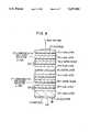
- FIG. 1is a sectional view showing a conventional light emitting device
- FIGS. 2, 3A and 3Bare energy band diagrams according to the conventional light emitting device
- FIG. 4is a sectional view showing a light emitting device of a first preferred embodiment according to the invention.
- FIGS. 5, 6A and 6Bare energy band diagrams of the preferred embodiment according to the invention.
- FIG. 7is a perspective view showing a light emitting device of a second preferred embodiment according to the invention.
- DBRsemiconductor multilayer reflector
- DBRsemiconductor multilayer reflector
- an n-semiconductor multilayer reflector (n-DBR) 12is formed on a substrate 10 of n-GaAs, and an n-clad layer 14 of Al 0 .3 Ga 0 .7 As, an active layer 16 of In 0 .2 Ga 0 .8 As and a p-clad layer 18 of Al 0 .3 Ga 0 .7 As are grown successively on the n-semiconductor multilayer reflector (n-DBR) 12.
- a p-semiconductor multilayer reflector (p-DBR) 20is formed on the p-clad layer 18.
- a p-electrode 22 of Auis formed on the p-semiconductor multilayer reflector (p-DBR) 20.
- an n-electrode 24 of AuGeNiis formed to have a window (not shown) for supplying light therethrough on the opposite surface of the substrate 10.
- the n-semiconductor multilayer reflector (n-DBR) 12consists of plural pairs of quarter-wavelength n-GaAs (high refractive index) layers 25 and quarter-wavelength n-AlAs (low refractive index) layers 26 which are grown alternately.
- the p-semiconductor multilayer reflector (p-DBR) 20consists of plural pairs of quarter-wavelength p-GaAs (high refractive index) layers 27 and quarter-wavelength p-AlAs (low refractive index) layers 28 which are grown alternately.
- FIG. 2shows an energy-band diagram on zero-bias condition
- FIG. 3Ashows more detail of the energy-band diagram of the n-semiconductor multilayer reflector (n-DBR) 12.
- reference numbers 32, 34 and 36indicate a conduction band level, a Fermi energy level, and a valence band level, respectively.
- potential barriers 30 (30a, 30b)occur on the conduction band 32 in the heterointerfaces, because band gap is largely different between the GaAs layer 25 and the AlAs layer 26.
- FIG. 3Bshows the energy-band diagram on bias condition.
- the potential barrier 30ais grown on the negative bias side ((-) electrical side).
- the level of the potential barrier 30adepends on difference of electron affinity between the GaAs layer 25 and the AlAs layer 26 and level of the bias voltage
- the width of the potential barrier 30adepends on doping concentration and dielectric constant of the layers 25 and 26 on the both sides of the interface. For instance, when the doping concentration is 1.5 ⁇ 10 17 cm -3 and the bias voltage is 0 V, the width of the potential barrier becomes about 200 ⁇ .
- the potential barriers 30 (30a, 30b)impede carriers flowing in the reflector (n-DBR) 12 and result in a large series resistance. Therefore, voltage drop occurs in carrier depletion regions of heterointerfaces, so that it is difficult to drive the light emitting device by a small bias voltage.
- the p-semiconductor multilayer reflector (p-DBR) 20is almost identical in energy band characteristic to the n-semiconductor multilayer reflector (n-DBR) 12 shown in FIGS. 3A and 3B, so that its explanation is omitted.
- an n-semiconductor multilayer reflector (n-DBR) 12is formed on a substrate 10 of n-GaAs, and an n-clad layer 14 of Al 0 .3 Ga 0 .7 As for phase control, an active layer 16 of In 0 .2 Ga 0 .8 As having a thickness of 100 ⁇ and a p-clad layer 18 of Al 0 .3 Ga 0 .7 As for phase control are grown successively on the n-semiconductor multilayer reflector (n-DBR) 12.
- n-semiconductor multilayer reflector (n-DBR) 12consists of 20 pairs of quarter-wavelength n-GaAs (high refractive index) layers 25 and quarter-wavelength n-AlAs (low refractive index) layers 26 which are grown alternately.
- n-impurity doping regions 50having a high concentration of 1 ⁇ 10 13 cm -2 and a delta functional width of several atoms (20 ⁇ ) are formed under the respective n-AlAs layers 26 by molecular beam epitaxy (MBE) method.
- MBEmolecular beam epitaxy
- a p-semiconductor multilayer reflector (p-DBR) 20is formed on the p-clad layer 18.
- the p-semiconductor multilayer reflector (p-DBR) 20consists of 15 pairs of quarter-wavelength p-GaAs (high refractive index) layers 27 quarter-wavelength p-AlAs (low refractive index) layers 28 which are grown alternately.
- p-impurity doping regions 52having a high concentration of 1 ⁇ 10 13 cm -2 and a delta functional width of several atoms (20 ⁇ ) are formed above the respective p-AlAs layers 28 by molecular beam epitaxy (MBE) method.
- MBEmolecular beam epitaxy
- a p-electrode 22 of Auis formed on the p-semiconductor multilayer reflector (p-DBR) 20.
- an n-electrode 24 of AuGeNiis formed to have a window 24A for supplying light therethrough, on the opposite surface of the substrate 10.
- the above fabricated structureis shaped to be cylindrical by etching. In this structure, "quarter-wavelength" defines a thickness of the layers equal to one fourth of a wavelength of light propagating through the layers.
- FIG. 5is an energy-band diagram depending on doping concentration on zero-bias condition
- FIG. 6Ashows more detail of the energy-band diagram of the n-semiconductor multilayer reflector (n-DBR) 12
- FIG. 6Bshows the energy-band diagram on bias condition.
- reference numbers 32, 34 and 36indicate a conduction band level, a Fermi energy level, and a valence band level, respectively.
- a potential barrier 56 on the conduction band 32 at a heterointerfacehas a width "d" of only 20 ⁇ , because the doping region 50 is formed at the heterointerface.
- tunnel current flowing through the multilayer reflectors (DBRs) 12 and 20is increased, so that a serial resistance is much decreased, for instance two figures, in comparison with the conventional light emitting device in which impurity is doped uniformity in the multilayer reflectors (DBRs).
- the light emitting devicecan be driven by small bias voltage.
- FIG. 7shows a light emitting device of a second preferred embodiment according to the invention, wherein like parts are indicated by like reference numerals as used in FIG. 4.
- the light emitting deviceis of a mesa type having a cylindrical structure provided on the substrate 10 which is fabricated by etching the structure of FIG. 4.
- the n-electrode 24is not provided with a window. In the practical use, such a window may be provided in either one of the p-and n-electrodes 22 and 24.
- the distance between the doping regions (50 and 52) and the heterointerfacesis not only limited by 20 ⁇ , but it may be 0 to 100 ⁇ distance.
- the impurity doping regions 50 and 52are formed in the both reflectors 12 and 20 in the above embodiments, however, the doping regions may be formed in one of the reflectors. And, the doping regions may be formed in part of the reflector.
- the semiconductor multilayer reflector according to the inventionis applicable not only to a surface-emitting laser, but also to other light emitting devices, such as a super-radiant type LED, PNPN-surface emitting device and switching device, etc.
Landscapes
- Physics & Mathematics (AREA)
- Condensed Matter Physics & Semiconductors (AREA)
- General Physics & Mathematics (AREA)
- Electromagnetism (AREA)
- Optics & Photonics (AREA)
- Semiconductor Lasers (AREA)
Abstract
Description
Claims (8)
Applications Claiming Priority (4)
| Application Number | Priority Date | Filing Date | Title |
|---|---|---|---|
| JP2-307647 | 1990-11-14 | ||
| JP30764790AJP2591333B2 (en) | 1990-11-14 | 1990-11-14 | Semiconductor light emitting device |
| JP3-000644 | 1991-01-08 | ||
| JP64491AJP2699661B2 (en) | 1991-01-08 | 1991-01-08 | Semiconductor multilayer reflective film |
Publications (1)
| Publication Number | Publication Date |
|---|---|
| US5237581Atrue US5237581A (en) | 1993-08-17 |
Family
ID=26333666
Family Applications (1)
| Application Number | Title | Priority Date | Filing Date |
|---|---|---|---|
| US07/791,264Expired - LifetimeUS5237581A (en) | 1990-11-14 | 1991-11-13 | Semiconductor multilayer reflector and light emitting device with the same |
Country Status (1)
| Country | Link |
|---|---|
| US (1) | US5237581A (en) |
Cited By (62)
| Publication number | Priority date | Publication date | Assignee | Title |
|---|---|---|---|---|
| US5338944A (en)* | 1993-09-22 | 1994-08-16 | Cree Research, Inc. | Blue light-emitting diode with degenerate junction structure |
| US5362974A (en)* | 1992-06-10 | 1994-11-08 | The Furukawa Electric Co., Ltd. | Group II-VI material semiconductor optical device with strained multiquantum barriers |
| US5373520A (en)* | 1992-08-12 | 1994-12-13 | Fujitsu Limited | Surface emitting laser and method of manufacturing the same |
| US5392307A (en)* | 1993-03-15 | 1995-02-21 | Fujitsu Limited | Vertical optoelectronic semiconductor device |
| US5543638A (en)* | 1993-08-20 | 1996-08-06 | Asea Brown Boveri Ab | Semiconductor light emitting device |
| US5568499A (en)* | 1995-04-07 | 1996-10-22 | Sandia Corporation | Optical device with low electrical and thermal resistance bragg reflectors |
| EP0760545A1 (en)* | 1995-08-28 | 1997-03-05 | Motorola, Inc. | Short wavelength VSCEL with al-free active region |
| US5625637A (en)* | 1991-03-28 | 1997-04-29 | Seiko Epson Corporation | Surface emitting semiconductor laser and its manufacturing process |
| US5670789A (en)* | 1994-12-08 | 1997-09-23 | Nec Corporation | Semiconductor light-emitting device with quantum well structure |
| US5745515A (en)* | 1996-07-18 | 1998-04-28 | Honeywell Inc. | Self-limiting intrinsically eye-safe laser utilizing an increasing absorption layer |
| US5774487A (en)* | 1996-10-16 | 1998-06-30 | Honeywell Inc. | Filamented multi-wavelength vertical-cavity surface emitting laser |
| US5799030A (en)* | 1996-07-26 | 1998-08-25 | Honeywell Inc. | Semiconductor device with a laser and a photodetector in a common container |
| EP0840306A3 (en)* | 1996-10-29 | 1998-09-16 | Samsung Electronics Co., Ltd. | Compatible optical pickup capable of scanning multiple tracks |
| US5812581A (en)* | 1996-07-26 | 1998-09-22 | Honeywell Inc. | Lens for a semiconductive device with a laser and a photodetector in a common container |
| US5940422A (en)* | 1996-06-28 | 1999-08-17 | Honeywell Inc. | Laser with an improved mode control |
| US5978401A (en)* | 1995-10-25 | 1999-11-02 | Honeywell Inc. | Monolithic vertical cavity surface emitting laser and resonant cavity photodetector transceiver |
| US6064076A (en)* | 1998-05-20 | 2000-05-16 | Visual Photonics Epitaxy Co., Ltd. | Light-emitting diode having a transparent substrate |
| US6222207B1 (en)* | 1999-05-24 | 2001-04-24 | Lumileds Lighting, U.S. Llc | Diffusion barrier for increased mirror reflectivity in reflective solderable contacts on high power LED chip |
| US6258699B1 (en) | 1999-05-10 | 2001-07-10 | Visual Photonics Epitaxy Co., Ltd. | Light emitting diode with a permanent subtrate of transparent glass or quartz and the method for manufacturing the same |
| US20010030318A1 (en)* | 1994-12-02 | 2001-10-18 | Shuji Nakamura | Nitride semiconductor light-emitting device |
| US20020085610A1 (en)* | 2000-12-29 | 2002-07-04 | Morgan Robert A. | Spatially modulated reflector for an optoelectronic device |
| US20020106160A1 (en)* | 2000-12-29 | 2002-08-08 | Honeywell International Inc. | Resonant reflector for increased wavelength and polarization control |
| US6577658B1 (en) | 1999-09-20 | 2003-06-10 | E20 Corporation, Inc. | Method and apparatus for planar index guided vertical cavity surface emitting lasers |
| US6580099B2 (en) | 1994-12-02 | 2003-06-17 | Nichia Chemical Industries, Ltd. | Nitride semiconductor light-emitting devices |
| US6586875B1 (en)* | 2000-08-10 | 2003-07-01 | United Epitaxy Company, Inc. | Light emitting diode with low-temperature solder layer |
| US6606199B2 (en) | 2001-10-10 | 2003-08-12 | Honeywell International Inc. | Graded thickness optical element and method of manufacture therefor |
| US20030213969A1 (en)* | 2001-11-16 | 2003-11-20 | Emcore Corporation | GaN based LED lighting extraction efficiency using digital diffractive phase grating |
| US20040042518A1 (en)* | 2002-09-03 | 2004-03-04 | Tatum James A. | Single mode VCSEL |
| US20040066820A1 (en)* | 2000-11-28 | 2004-04-08 | Johnson Ralph H. | Versatile method and system for single mode VCSELs |
| US20040081215A1 (en)* | 2002-10-28 | 2004-04-29 | Honeywell International Inc. | Distributed bragg reflector for optoelectronic device |
| US20040101009A1 (en)* | 2002-11-21 | 2004-05-27 | Honeywell International Inc. | Long wavelength VCSEL with tunnel junction, and implant |
| US6782027B2 (en) | 2000-12-29 | 2004-08-24 | Finisar Corporation | Resonant reflector for use with optoelectronic devices |
| US20040222363A1 (en)* | 2003-05-07 | 2004-11-11 | Honeywell International Inc. | Connectorized optical component misalignment detection system |
| US20040247250A1 (en)* | 2003-06-03 | 2004-12-09 | Honeywell International Inc. | Integrated sleeve pluggable package |
| US20040264536A1 (en)* | 2003-06-27 | 2004-12-30 | Honeywell International Inc. | Dielectric VCSEL gain guide |
| US20040264530A1 (en)* | 2003-06-27 | 2004-12-30 | Honeywell International Inc. | VCSEL having thermal management |
| US20050013542A1 (en)* | 2003-07-16 | 2005-01-20 | Honeywell International Inc. | Coupler having reduction of reflections to light source |
| US20050014390A1 (en)* | 2003-07-18 | 2005-01-20 | Honeywell International Inc. | Edge bead control method and apparatus |
| US20050013539A1 (en)* | 2003-07-17 | 2005-01-20 | Honeywell International Inc. | Optical coupling system |
| US20050013553A1 (en)* | 2003-07-16 | 2005-01-20 | Honeywell International Inc. | Optical coupling system |
| US20050031011A1 (en)* | 2000-11-28 | 2005-02-10 | Biard James R. | Electron affinity engineered VCSELs |
| US20050036533A1 (en)* | 2000-12-29 | 2005-02-17 | Honeywell To Finisar | Tunable detector |
| US20050092710A1 (en)* | 2003-10-29 | 2005-05-05 | Biard James R. | Long wavelength VCSEL device processing |
| US6900472B2 (en) | 1997-12-15 | 2005-05-31 | Lumileds Lighting U.S., Llc | Semiconductor light emitting device having a silver p-contact |
| US6946685B1 (en) | 2000-08-31 | 2005-09-20 | Lumileds Lighting U.S., Llc | Light emitting semiconductor method and device |
| US6961489B2 (en) | 2003-06-30 | 2005-11-01 | Finisar Corporation | High speed optical system |
| US20060045162A1 (en)* | 2004-08-31 | 2006-03-02 | Finisar Corporation | Distributed bragg reflector for optoelectronic device |
| US20060056762A1 (en)* | 2003-07-02 | 2006-03-16 | Honeywell International Inc. | Lens optical coupler |
| US20060054908A1 (en)* | 2004-08-12 | 2006-03-16 | Hironobu Sai | Semiconductor light-emitting device |
| US7054345B2 (en) | 2003-06-27 | 2006-05-30 | Finisar Corporation | Enhanced lateral oxidation |
| US20060268954A1 (en)* | 2004-08-31 | 2006-11-30 | Johnson Ralph H | Light emitting semiconductor device having an electrical confinement barrier near the active region |
| US7149383B2 (en) | 2003-06-30 | 2006-12-12 | Finisar Corporation | Optical system with reduced back reflection |
| US20070012937A1 (en)* | 2005-07-12 | 2007-01-18 | Jin-Hsiang Liu | High-brightness light emitting diode having reflective layer |
| US20070020788A1 (en)* | 2005-07-12 | 2007-01-25 | Jin-Hsiang Liu | Fabrication method of high-brightness light emitting diode having reflective layer |
| US7298942B2 (en) | 2003-06-06 | 2007-11-20 | Finisar Corporation | Pluggable optical optic system having a lens fiber stop |
| US20080023688A1 (en)* | 2006-07-31 | 2008-01-31 | Finisar Corporation | Efficient carrier injection in a semiconductor device |
| US7433381B2 (en) | 2003-06-25 | 2008-10-07 | Finisar Corporation | InP based long wavelength VCSEL |
| US20100012962A1 (en)* | 2008-07-17 | 2010-01-21 | Advanced Optoelectronic Technology Inc. | Light emitting diode and fabrication thereof |
| US8031752B1 (en) | 2007-04-16 | 2011-10-04 | Finisar Corporation | VCSEL optimized for high speed data |
| US8189642B1 (en) | 2007-08-08 | 2012-05-29 | Emcore Corporation | VCSEL semiconductor device |
| US20130234108A1 (en)* | 2012-03-06 | 2013-09-12 | Soraa, Inc. | Light emitting diodes with low refractive index material layers to reduce light guiding effects |
| US10453992B2 (en)* | 2016-04-29 | 2019-10-22 | Xiamen Sanan Optoelectron Co., Ltd. | Light emitting diode |
Citations (1)
| Publication number | Priority date | Publication date | Assignee | Title |
|---|---|---|---|---|
| US5012486A (en)* | 1990-04-06 | 1991-04-30 | At&T Bell Laboratories | Vertical cavity semiconductor laser with lattice-mismatched mirror stack |
- 1991
- 1991-11-13USUS07/791,264patent/US5237581A/ennot_activeExpired - Lifetime
Patent Citations (1)
| Publication number | Priority date | Publication date | Assignee | Title |
|---|---|---|---|---|
| US5012486A (en)* | 1990-04-06 | 1991-04-30 | At&T Bell Laboratories | Vertical cavity semiconductor laser with lattice-mismatched mirror stack |
Cited By (106)
| Publication number | Priority date | Publication date | Assignee | Title |
|---|---|---|---|---|
| US5625637A (en)* | 1991-03-28 | 1997-04-29 | Seiko Epson Corporation | Surface emitting semiconductor laser and its manufacturing process |
| US5362974A (en)* | 1992-06-10 | 1994-11-08 | The Furukawa Electric Co., Ltd. | Group II-VI material semiconductor optical device with strained multiquantum barriers |
| US5373520A (en)* | 1992-08-12 | 1994-12-13 | Fujitsu Limited | Surface emitting laser and method of manufacturing the same |
| US5392307A (en)* | 1993-03-15 | 1995-02-21 | Fujitsu Limited | Vertical optoelectronic semiconductor device |
| US5543638A (en)* | 1993-08-20 | 1996-08-06 | Asea Brown Boveri Ab | Semiconductor light emitting device |
| US5338944A (en)* | 1993-09-22 | 1994-08-16 | Cree Research, Inc. | Blue light-emitting diode with degenerate junction structure |
| US6900465B2 (en) | 1994-12-02 | 2005-05-31 | Nichia Corporation | Nitride semiconductor light-emitting device |
| US20010030318A1 (en)* | 1994-12-02 | 2001-10-18 | Shuji Nakamura | Nitride semiconductor light-emitting device |
| US6580099B2 (en) | 1994-12-02 | 2003-06-17 | Nichia Chemical Industries, Ltd. | Nitride semiconductor light-emitting devices |
| US5670789A (en)* | 1994-12-08 | 1997-09-23 | Nec Corporation | Semiconductor light-emitting device with quantum well structure |
| US5568499A (en)* | 1995-04-07 | 1996-10-22 | Sandia Corporation | Optical device with low electrical and thermal resistance bragg reflectors |
| EP0760545A1 (en)* | 1995-08-28 | 1997-03-05 | Motorola, Inc. | Short wavelength VSCEL with al-free active region |
| US5978401A (en)* | 1995-10-25 | 1999-11-02 | Honeywell Inc. | Monolithic vertical cavity surface emitting laser and resonant cavity photodetector transceiver |
| US5940422A (en)* | 1996-06-28 | 1999-08-17 | Honeywell Inc. | Laser with an improved mode control |
| US5745515A (en)* | 1996-07-18 | 1998-04-28 | Honeywell Inc. | Self-limiting intrinsically eye-safe laser utilizing an increasing absorption layer |
| US5799030A (en)* | 1996-07-26 | 1998-08-25 | Honeywell Inc. | Semiconductor device with a laser and a photodetector in a common container |
| US5812581A (en)* | 1996-07-26 | 1998-09-22 | Honeywell Inc. | Lens for a semiconductive device with a laser and a photodetector in a common container |
| US5774487A (en)* | 1996-10-16 | 1998-06-30 | Honeywell Inc. | Filamented multi-wavelength vertical-cavity surface emitting laser |
| US6023450A (en)* | 1996-10-29 | 2000-02-08 | Samsung Electronics Co., Ltd. | Multiple beam optical pickup using a vertical cavity surface emitting laser array |
| EP0840306A3 (en)* | 1996-10-29 | 1998-09-16 | Samsung Electronics Co., Ltd. | Compatible optical pickup capable of scanning multiple tracks |
| US20050179051A1 (en)* | 1997-12-15 | 2005-08-18 | You Kondoh | III-Nitride semiconductor light emitting device having a silver p-contact |
| US7262436B2 (en) | 1997-12-15 | 2007-08-28 | Philips Lumileds Lighting Company, Llc | III-nitride semiconductor light emitting device having a silver p-contact |
| US6900472B2 (en) | 1997-12-15 | 2005-05-31 | Lumileds Lighting U.S., Llc | Semiconductor light emitting device having a silver p-contact |
| US6064076A (en)* | 1998-05-20 | 2000-05-16 | Visual Photonics Epitaxy Co., Ltd. | Light-emitting diode having a transparent substrate |
| US6258699B1 (en) | 1999-05-10 | 2001-07-10 | Visual Photonics Epitaxy Co., Ltd. | Light emitting diode with a permanent subtrate of transparent glass or quartz and the method for manufacturing the same |
| US6222207B1 (en)* | 1999-05-24 | 2001-04-24 | Lumileds Lighting, U.S. Llc | Diffusion barrier for increased mirror reflectivity in reflective solderable contacts on high power LED chip |
| US6593160B2 (en) | 1999-05-24 | 2003-07-15 | Lumileds Lighting, U.S., Llc | Diffusion barrier for increased mirror reflectivity in reflective solderable contacts on high power led chip |
| US6852558B2 (en) | 1999-09-20 | 2005-02-08 | Jds Uniphase Corporation | Methods for forming index guided vertical cavity surface emitting lasers |
| US6822993B2 (en) | 1999-09-20 | 2004-11-23 | Jds Uniphase Corporation | Index guided vertical cavity surface emitting lasers |
| US6577658B1 (en) | 1999-09-20 | 2003-06-10 | E20 Corporation, Inc. | Method and apparatus for planar index guided vertical cavity surface emitting lasers |
| US6586875B1 (en)* | 2000-08-10 | 2003-07-01 | United Epitaxy Company, Inc. | Light emitting diode with low-temperature solder layer |
| US6946685B1 (en) | 2000-08-31 | 2005-09-20 | Lumileds Lighting U.S., Llc | Light emitting semiconductor method and device |
| US7065124B2 (en) | 2000-11-28 | 2006-06-20 | Finlsar Corporation | Electron affinity engineered VCSELs |
| US6905900B1 (en) | 2000-11-28 | 2005-06-14 | Finisar Corporation | Versatile method and system for single mode VCSELs |
| US20040066819A1 (en)* | 2000-11-28 | 2004-04-08 | Johnson Ralph H. | Versatile method and system for single mode VCSELs |
| US20040066820A1 (en)* | 2000-11-28 | 2004-04-08 | Johnson Ralph H. | Versatile method and system for single mode VCSELs |
| US7221691B2 (en) | 2000-11-28 | 2007-05-22 | Finisar Corporation | Versatile method and system for single mode VCSELs |
| US20050031011A1 (en)* | 2000-11-28 | 2005-02-10 | Biard James R. | Electron affinity engineered VCSELs |
| US20040213311A1 (en)* | 2000-11-28 | 2004-10-28 | Johnson Ralph H | Single mode vertical cavity surface emitting laser |
| US7308011B2 (en) | 2000-11-28 | 2007-12-11 | Finisar Corporation | Versatile method and system for single mode VCSELs |
| US20050036533A1 (en)* | 2000-12-29 | 2005-02-17 | Honeywell To Finisar | Tunable detector |
| US6727520B2 (en) | 2000-12-29 | 2004-04-27 | Honeywell International Inc. | Spatially modulated reflector for an optoelectronic device |
| US7266135B2 (en) | 2000-12-29 | 2007-09-04 | Finisar Corporation | Method for producing laser with resonant reflector |
| US6836501B2 (en) | 2000-12-29 | 2004-12-28 | Finisar Corporation | Resonant reflector for increased wavelength and polarization control |
| US20020106160A1 (en)* | 2000-12-29 | 2002-08-08 | Honeywell International Inc. | Resonant reflector for increased wavelength and polarization control |
| US6782027B2 (en) | 2000-12-29 | 2004-08-24 | Finisar Corporation | Resonant reflector for use with optoelectronic devices |
| US8599897B2 (en) | 2000-12-29 | 2013-12-03 | Finisar Corporation | Tunable detector |
| US7760786B2 (en) | 2000-12-29 | 2010-07-20 | Finisar Corporation | Laser with resonant reflector |
| US7288421B2 (en) | 2000-12-29 | 2007-10-30 | Finisar Corporation | Method for forming an optoelectronic device having an isolation layer |
| US20020085610A1 (en)* | 2000-12-29 | 2002-07-04 | Morgan Robert A. | Spatially modulated reflector for an optoelectronic device |
| US20040191941A1 (en)* | 2000-12-29 | 2004-09-30 | Morgan Robert A. | Method for producing laser with resonant reflector |
| US20040188695A1 (en)* | 2000-12-29 | 2004-09-30 | Morgan Robert A. | Laser with resonant reflector |
| US6606199B2 (en) | 2001-10-10 | 2003-08-12 | Honeywell International Inc. | Graded thickness optical element and method of manufacture therefor |
| US20030213969A1 (en)* | 2001-11-16 | 2003-11-20 | Emcore Corporation | GaN based LED lighting extraction efficiency using digital diffractive phase grating |
| US6903379B2 (en) | 2001-11-16 | 2005-06-07 | Gelcore Llc | GaN based LED lighting extraction efficiency using digital diffractive phase grating |
| US20040042518A1 (en)* | 2002-09-03 | 2004-03-04 | Tatum James A. | Single mode VCSEL |
| US6965626B2 (en) | 2002-09-03 | 2005-11-15 | Finisar Corporation | Single mode VCSEL |
| US20040081215A1 (en)* | 2002-10-28 | 2004-04-29 | Honeywell International Inc. | Distributed bragg reflector for optoelectronic device |
| US20050190812A1 (en)* | 2002-10-28 | 2005-09-01 | Johnson Ralph H. | Distributed bragg reflector for optoelectronic device |
| US7251264B2 (en) | 2002-10-28 | 2007-07-31 | Finisar Corporation | Distributed bragg reflector for optoelectronic device |
| US6990135B2 (en) | 2002-10-28 | 2006-01-24 | Finisar Corporation | Distributed bragg reflector for optoelectronic device |
| US20040101009A1 (en)* | 2002-11-21 | 2004-05-27 | Honeywell International Inc. | Long wavelength VCSEL with tunnel junction, and implant |
| US6813293B2 (en) | 2002-11-21 | 2004-11-02 | Finisar Corporation | Long wavelength VCSEL with tunnel junction, and implant |
| US20040222363A1 (en)* | 2003-05-07 | 2004-11-11 | Honeywell International Inc. | Connectorized optical component misalignment detection system |
| US20040247250A1 (en)* | 2003-06-03 | 2004-12-09 | Honeywell International Inc. | Integrated sleeve pluggable package |
| US7298942B2 (en) | 2003-06-06 | 2007-11-20 | Finisar Corporation | Pluggable optical optic system having a lens fiber stop |
| US7433381B2 (en) | 2003-06-25 | 2008-10-07 | Finisar Corporation | InP based long wavelength VCSEL |
| US7277461B2 (en) | 2003-06-27 | 2007-10-02 | Finisar Corporation | Dielectric VCSEL gain guide |
| US20040264530A1 (en)* | 2003-06-27 | 2004-12-30 | Honeywell International Inc. | VCSEL having thermal management |
| US7054345B2 (en) | 2003-06-27 | 2006-05-30 | Finisar Corporation | Enhanced lateral oxidation |
| US20040264536A1 (en)* | 2003-06-27 | 2004-12-30 | Honeywell International Inc. | Dielectric VCSEL gain guide |
| US7075962B2 (en) | 2003-06-27 | 2006-07-11 | Finisar Corporation | VCSEL having thermal management |
| US7149383B2 (en) | 2003-06-30 | 2006-12-12 | Finisar Corporation | Optical system with reduced back reflection |
| US7139454B2 (en) | 2003-06-30 | 2006-11-21 | Finisar Corporation | Methods for signal transmission in optical fiber |
| US6961489B2 (en) | 2003-06-30 | 2005-11-01 | Finisar Corporation | High speed optical system |
| US20060056762A1 (en)* | 2003-07-02 | 2006-03-16 | Honeywell International Inc. | Lens optical coupler |
| US20050013542A1 (en)* | 2003-07-16 | 2005-01-20 | Honeywell International Inc. | Coupler having reduction of reflections to light source |
| US20050013553A1 (en)* | 2003-07-16 | 2005-01-20 | Honeywell International Inc. | Optical coupling system |
| US7210857B2 (en) | 2003-07-16 | 2007-05-01 | Finisar Corporation | Optical coupling system |
| US20050013539A1 (en)* | 2003-07-17 | 2005-01-20 | Honeywell International Inc. | Optical coupling system |
| US6887801B2 (en) | 2003-07-18 | 2005-05-03 | Finisar Corporation | Edge bead control method and apparatus |
| US20050014390A1 (en)* | 2003-07-18 | 2005-01-20 | Honeywell International Inc. | Edge bead control method and apparatus |
| US7031363B2 (en) | 2003-10-29 | 2006-04-18 | Finisar Corporation | Long wavelength VCSEL device processing |
| US20050092710A1 (en)* | 2003-10-29 | 2005-05-05 | Biard James R. | Long wavelength VCSEL device processing |
| US20060054908A1 (en)* | 2004-08-12 | 2006-03-16 | Hironobu Sai | Semiconductor light-emitting device |
| US7173287B2 (en)* | 2004-08-12 | 2007-02-06 | Rohm Co., Ltd. | Semiconductor light-emitting device |
| US20060045162A1 (en)* | 2004-08-31 | 2006-03-02 | Finisar Corporation | Distributed bragg reflector for optoelectronic device |
| US7920612B2 (en) | 2004-08-31 | 2011-04-05 | Finisar Corporation | Light emitting semiconductor device having an electrical confinement barrier near the active region |
| US7596165B2 (en) | 2004-08-31 | 2009-09-29 | Finisar Corporation | Distributed Bragg Reflector for optoelectronic device |
| US20060268954A1 (en)* | 2004-08-31 | 2006-11-30 | Johnson Ralph H | Light emitting semiconductor device having an electrical confinement barrier near the active region |
| US7384808B2 (en) | 2005-07-12 | 2008-06-10 | Visual Photonics Epitaxy Co., Ltd. | Fabrication method of high-brightness light emitting diode having reflective layer |
| US7335924B2 (en) | 2005-07-12 | 2008-02-26 | Visual Photonics Epitaxy Co., Ltd. | High-brightness light emitting diode having reflective layer |
| US20070012937A1 (en)* | 2005-07-12 | 2007-01-18 | Jin-Hsiang Liu | High-brightness light emitting diode having reflective layer |
| US20070020788A1 (en)* | 2005-07-12 | 2007-01-25 | Jin-Hsiang Liu | Fabrication method of high-brightness light emitting diode having reflective layer |
| US7829912B2 (en) | 2006-07-31 | 2010-11-09 | Finisar Corporation | Efficient carrier injection in a semiconductor device |
| US20080023688A1 (en)* | 2006-07-31 | 2008-01-31 | Finisar Corporation | Efficient carrier injection in a semiconductor device |
| US8031752B1 (en) | 2007-04-16 | 2011-10-04 | Finisar Corporation | VCSEL optimized for high speed data |
| US8189642B1 (en) | 2007-08-08 | 2012-05-29 | Emcore Corporation | VCSEL semiconductor device |
| US8278645B2 (en) | 2008-07-17 | 2012-10-02 | Advanced Optoelectronic Technology, Inc. | Light emitting diode and fabrication thereof |
| US20100012962A1 (en)* | 2008-07-17 | 2010-01-21 | Advanced Optoelectronic Technology Inc. | Light emitting diode and fabrication thereof |
| US20130234108A1 (en)* | 2012-03-06 | 2013-09-12 | Soraa, Inc. | Light emitting diodes with low refractive index material layers to reduce light guiding effects |
| US9269876B2 (en)* | 2012-03-06 | 2016-02-23 | Soraa, Inc. | Light emitting diodes with low refractive index material layers to reduce light guiding effects |
| US20160172556A1 (en)* | 2012-03-06 | 2016-06-16 | Soraa, Inc. | Light emitting diode with low refractive index material layers to reduce light guiding effects |
| US10096755B2 (en)* | 2012-03-06 | 2018-10-09 | Soraa, Inc. | Light emitting diode with low refractive index material layers to reduce light guiding effects |
| US20190140150A1 (en)* | 2012-03-06 | 2019-05-09 | Soraa, Inc. | Light emitting diode with low refractive index material layers to reduce light guiding effects |
| US10453992B2 (en)* | 2016-04-29 | 2019-10-22 | Xiamen Sanan Optoelectron Co., Ltd. | Light emitting diode |
Similar Documents
| Publication | Publication Date | Title |
|---|---|---|
| US5237581A (en) | Semiconductor multilayer reflector and light emitting device with the same | |
| US5568499A (en) | Optical device with low electrical and thermal resistance bragg reflectors | |
| US5892787A (en) | N-drive, p-common light-emitting devices fabricated on an n-type substrate and method of making same | |
| US5724376A (en) | Transparent substrate vertical cavity surface emitting lasers fabricated by semiconductor wafer bonding | |
| US7016392B2 (en) | GaAs-based long-wavelength laser incorporating tunnel junction structure | |
| KR100523484B1 (en) | Method for fabricating semiconductor optical devices having current-confined structure | |
| US7638792B2 (en) | Tunnel junction light emitting device | |
| US6711195B2 (en) | Long-wavelength photonic device with GaAsSb quantum-well layer | |
| EP1459417B1 (en) | Asymmetric distributed bragg reflector for vertical cavity surface emitting lasers | |
| US5392307A (en) | Vertical optoelectronic semiconductor device | |
| EP1025593A1 (en) | Semiconductor with tunnel hole contact sources | |
| EP0261262B1 (en) | Transverse junction stripe laser | |
| CN1780004A (en) | A Vertical Cavity Optoelectronic Device Containing Tunnel Junction | |
| KR20020059663A (en) | LONG WAVELENGTH PSEUDOMORPHIC InGaNPAsSb TYPE-I AND TYPE-II ACTIVE LAYERS FOR THE GAAS MATERIAL SYSTEM | |
| CN115398761B (en) | Two-dimensional photonic crystal lasers | |
| US5208820A (en) | Optical device with low-resistive multi-level reflecting structure | |
| US6728283B2 (en) | Semiconductor laser and photo module using the same | |
| US6859474B1 (en) | Long wavelength pseudomorphic InGaNPAsSb type-I and type-II active layers for the gaas material system | |
| JP2699661B2 (en) | Semiconductor multilayer reflective film | |
| KR100545113B1 (en) | Vertical Common Surface Emission Laser with Visible Wavelength | |
| JPH05211346A (en) | Surface light emitting element | |
| JP2757633B2 (en) | Surface emitting semiconductor laser | |
| JP3223969B2 (en) | Semiconductor laser | |
| JPH04280693A (en) | Surface emission laser | |
| JPH05175535A (en) | Quantized Si optical semiconductor device |
Legal Events
| Date | Code | Title | Description |
|---|---|---|---|
| AS | Assignment | Owner name:NEC CORPORATION Free format text:ASSIGNMENT OF ASSIGNORS INTEREST.;ASSIGNORS:ASADA, SUSUMU;KURIHARA, KAORI;REEL/FRAME:005983/0183 Effective date:19911113 Owner name:NEC CORPORATION, JAPAN Free format text:ASSIGNMENT OF ASSIGNORS INTEREST;ASSIGNORS:ASADA, SUSUMU;KURIHARA, KAORI;REEL/FRAME:005983/0183 Effective date:19911113 | |
| STCF | Information on status: patent grant | Free format text:PATENTED CASE | |
| FPAY | Fee payment | Year of fee payment:4 | |
| FEPP | Fee payment procedure | Free format text:PAYOR NUMBER ASSIGNED (ORIGINAL EVENT CODE: ASPN); ENTITY STATUS OF PATENT OWNER: LARGE ENTITY | |
| FEPP | Fee payment procedure | Free format text:PAYER NUMBER DE-ASSIGNED (ORIGINAL EVENT CODE: RMPN); ENTITY STATUS OF PATENT OWNER: LARGE ENTITY Free format text:PAYOR NUMBER ASSIGNED (ORIGINAL EVENT CODE: ASPN); ENTITY STATUS OF PATENT OWNER: LARGE ENTITY | |
| FPAY | Fee payment | Year of fee payment:8 | |
| FPAY | Fee payment | Year of fee payment:12 |