US5237346A - Integrated thin film transistor electrographic writing head - Google Patents
Integrated thin film transistor electrographic writing headDownload PDFInfo
- Publication number
- US5237346A US5237346AUS07/871,250US87125092AUS5237346AUS 5237346 AUS5237346 AUS 5237346AUS 87125092 AUS87125092 AUS 87125092AUS 5237346 AUS5237346 AUS 5237346A
- Authority
- US
- United States
- Prior art keywords
- writing head
- writing
- thin film
- data
- electrographic
- Prior art date
- Legal status (The legal status is an assumption and is not a legal conclusion. Google has not performed a legal analysis and makes no representation as to the accuracy of the status listed.)
- Expired - Fee Related
Links
Images


Classifications
- G—PHYSICS
- G06—COMPUTING OR CALCULATING; COUNTING
- G06K—GRAPHICAL DATA READING; PRESENTATION OF DATA; RECORD CARRIERS; HANDLING RECORD CARRIERS
- G06K15/00—Arrangements for producing a permanent visual presentation of the output data, e.g. computer output printers
- G06K15/02—Arrangements for producing a permanent visual presentation of the output data, e.g. computer output printers using printers
- G06K15/14—Arrangements for producing a permanent visual presentation of the output data, e.g. computer output printers using printers by electrographic printing, e.g. xerography; by magnetographic printing
Definitions
- the writing headcomprises thin film elements including stylus electrodes or nibs, dynamic shift register elements or decoder elements, driving buffers, memory or static RAM (Random Access Memory) cells, latches and high voltage drivers.
- thin film elementsincluding stylus electrodes or nibs, dynamic shift register elements or decoder elements, driving buffers, memory or static RAM (Random Access Memory) cells, latches and high voltage drivers.
- Amorphous silicon, a-Si, technologyhas found numerous applications because of its low cost and compatibility with low temperature glass substrates. Circuits are regularly fabricated with linear dimensions in excess of 30 cm. Thin film transistors, TFTs, are widely used as pixel addressing elements in large area active matrix liquid crystal displays, and in printing and scanning bars. Printing systems upon lonography and Electrography have also been demonstrated with a-Si.
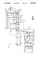
- FIG. 8An example of a typical electrographic writing head 10 is schematically illustrated in FIG. 8.
- Such a writing headmanufacturable by thin film fabrication techniques, is fully disclosed in U.S. Pat. No. 4,588,997 to Tuan et al. which is hereby incorporated by reference.
- An example fabrication techniqueis also discussed in U.S. Pat .No. 4,998,146 tohack.
- Writing head 10comprises a linear array of several thousand styli or nibs 12 for generating sequential raster line of information by means of high voltage electrical discharges across a minute air gap to a conductive electrode.
- a multiplexing schemeis used wherein the charge on each stylus is controlled by a low voltage thin film pass transistor (LVTFT) 14 which selectively charges and discharges the gate of a thin film high voltage transistor 16 for switching the HVTFT.
- LVTFTlow voltage thin film pass transistor
- This schemeallows each stylus to maintain its imposed charge, for substantially a line time, between charges and discharges.
- the drain electrode 18 of HVTFT 16is connected to high voltage bus 20 (maintained at about 450 voltage relative to ground) via load resistor 22, and its source electrode 24 is connected to ground bus 26.
- Data signals, from data lines 28, on the order of 20 volts (ON) and 0 voltage (OFF)will be imposed upon the gate electrode of the HVTFT when the address line 30 switches the gate of LVTFT 14 between about 24 volts (ON) and 0 volts (OFF) during "gate time" of about 15 to 25 microseconds, i.e. the time it takes for the gate of the HVTFT to reach its desired potential.
- a-Si TFTshave both a low mobility and a larger threshold voltage (1 V to 2V). As stated above, the mobility is nearly three orders of magnitude below crystal silicon. To partly compensate for the low current drive, higher operating voltages are used. The low voltage transistors can withstand gate to source potentials up to 40 V without failure. However even with the higher drive voltage, the gate select time is tens of microseconds.
- the device discussed hereinis a 400 driver per inch print array.
- the arrayhas 32 parallel data drivers per segments, resulting in 148 segments; each being controlled by a single select line.
- Such a large number of inputscan drive up the cost of the array interface significantly, for reasons already discussed. Since the speed requirements of the select lines is low, there is opportunity to reduce the number of inputs even further by moving the select line drive circuitry directly into the a-Si array.
- One methodis to integrate into the array an a-Si serial-in/parallel-out shift register; whereby shifting a single active bit down the register enables each of the segments in turn.
- Another configurationcould be the use of a dynamic shift register as described in cross-referenced application titled "Parallel Multi-Phased a-Si Shift Register for Fast Addressing of an a-Si Array". Use of such a shift register would allow the writing head to operate at a higher speed. Still another configuration could be to use an integrated decoder for selecting segments on the array. Although an a-Si device is described herein, it can be appreciated that the following invention could be made from non-crystalline silicon (e.g. poly-crystalline, micro-crystalline).
- the storage of data on the print headis dynamic, thus needing refresh.
- the necessary refreshadds additional burden to the computer interface since it must receive new data, store the data needed for the refresh, and schedule the transmission of new data between refresh cycles.
- the device of FIG. 8also presents data to the high voltage output drivers as the data is being written to the head. Movement of the media is in the process direction and one segments of an entire scanline is written at a time. For high speed wide format drivers (e.g. 36 inch), where three adjacent print heads are printing in parallel, this approach comprises horizontal or scanline (along the printhead) line quality.
- the datacould be presented to the high voltage output drivers all at once across the entire scanline after all of the memory is loaded and latched into place. Printing in this manner yields a higher degree of print quality.
- an integrated thin film transistor electrographic writing headcomprising: a plurality of marking electrodes arranged in a linear array for writing data onto a medium; a plurality of driving means the plurality of driving means providing drive for the plurality of marking electrodes; a plurality of latching means each connected to the driving means, the latching means for latching an entire scanline of the data across the writing head to be driven by the plurality driving means, a plurality of memory means each connected to the latching means for temporarily storing the data before latching by the plurality of latching means; a plurality of buffer means, each buffer means supplying a select signal to a specified group of the plurality of memory means; and a plurality of selecting means, the selecting means supplying a signal to each of the buffer means, to be driven by the buffer means, for loading data into a select number of the memory means.
- FIG. 1is a block diagram representation of an integral thin film transistor writing head of the present invention using a traditional shift register configuration, each block depicting a segment controlled by a single select line;
- FIG. 2is a schematic representation of a 32 bit segment of an integral thin film writing head of the present invention
- FIG. 3is a block diagram representation of an integral thin film transistor writing head of the present invention using a shift register configuration where each shift register element is clocked one quarter out of phase with the next shift register element;
- FIG. 4is a block diagram representation of the shift register configuration used in FIG. 3;
- FIG. 5is a timing diagram representing the clocks needed to drive the dynamic shift registers of FIGS. 1-4;
- FIG. 6is a block diagram representation of an integral thin film transistor writing head of the present invention using a decoder
- FIGS. 7a and 7bare a block diagram depicting a full width electrographic writing head which is manufactured from several smaller heads.
- FIG. 8is a schematic representation of an integral thin film writing head of the prior art.
- FIG. 1shown is a block diagram of one configuration of writing head 10 in accordance with the present invention.
- Head 10has several thirty-two big segments 11 aligned in a linear array.
- Each segment 11has a dynamic shift register element 50, a buffer 60, thirty-two static Random Access Memory (RAM) Elements 70, thirty-two bit latch elements 80, thirty-two high voltage cascode circuits 90 and thirty-two nibs 12 for writing data onto a medium.
- RAMstatic Random Access Memory
- each dynamic shift register 50has a buffer 60 at its output supplying a segment select line V G .
- each buffer 60drives the select lines of thirty-two RAM cells 70 which comprise a group in segment 11.
- latch circuit 80At the output of each of the thirty-two bit RAM cells 70 is latch circuit 80.
- Latch circuit 80supplies information to cascode circuit 90 which acts as a high voltage buffer driver to nib 12.
- writing head 10is comprised of several thousand nibs and their associated circuitry set forth in a linear array.
- segment 11 of write head 10is a thirty-two bit segment, it can be appreciated that any number of bits per segment can made.
- write input V Wis set low, thus disconnecting the high voltage cascode circuit 90 from the output of RAM cell 70.
- the output of cascode circuit 90will remain in its last state.
- all RAM cells 70 on head 10are set low by pulsing the present signal V PS high.
- a logic lowis shifted down dynamic shift register 50. This shifted logic low is buffered and inverted by buffer 60 at the output of each shift register 50 sequentially enabling the select line V G .
- the enablement of V Gselects each group of thirty-two RAM cells 70 in turn. As each group of RAM cells 70 is enabled, thirty-two bits of data from the data bus are loaded into the selected groups' RAM cells. If a data line is logic high, the RAM cell 70 is left with its output low.
- FIG. 2shown in a detailed schematic of thirty-two bit segment 11 of electrographic writing head 10.
- a four phase ratioless shift register 50 designis shown which provides a large switching range and allows for fast operating speed since no pull-up devices are used.
- Such a shift register and related bufferare described in detail and are the subject of cross-referenced application titled "Parallel Multi-Phased a-Si Shift Register for Fast Addressing of an a-Si Array".
- Four non-overlapping clock pulses, C1, C2, C3, C4as seen in FIG. 5 and represented during clock phases F 1 to F 4 , are used to drive shift register 50.
- Shift registers 50can e configured in a traditional setup as in FIG.
- each shift register element 50is clocked one quarter out of phase with the next adjacent shift register element.
- the purpose of shift register elements 50is to shift a select pulse sequentially down array 10 choosing groups within each segment 11 for loading of image data into RAM cells 70.
- buffer 60drives the select lines of a group of thirty-two RAM cells 70 concurrently.
- buffer 60is situated between the output bit of each shift register element 50 and the gate select line, V G of static ram cell 70.
- Buffer 60operates in a two phase mode, utilizing the two phases in which the output of dynamic shift register 50 is valid. Buffer 60 then provides the select signal pulse during one of the phases where the signal from shift register 50 is valid. The pulse delivered by the buffer 60 is inverted from the output of shift register 50, therefore a line time is accomplished by shifting a single active bit 0 (low) down shift register 50 rather than shifting a bit 1 (high).
- Static memory cell 70comprises cross-coupled inverters 72 and 74.
- Transistor Q PSis used to preset cell 70 and pass transistor Q P is used to transfer data from RAM 70 to latch 80. It can also be appreciated that other types of memory devices can also be integrated on the writing head successfully.
- Latch circuit 80comprises a low voltage thin film pass transistor 36. Latch 80 is placed between RAM cell 70 and cascode circuit 90, which is the driver of nib 12. At the start of scan, latch 80 is disabled so that cascode driver 90 is disconnected from RAM cell 70 where cascode circuit 90 maintains its state through the intrinsic capacitance of its gate electrode. All RAM cells 70 on the printing head are then preset in parallel via signal V PS . Data is then written to each thirty-two bit group of RAM cells 70 in segment 11. After an entire scanline of data has been written into all of the RAM cells 70 on the print head 10, all the latches 80 can be loaded in parallel by activating latching signal V W whereby transferring the data to nibs 12 through cascode circuit 90.
- Cascode circuit 90comprises a low voltage thin film switching transistor 38 (LVTFT) for switching the source electrode potential of a high voltage thin film transistor 16 (HVTFT) in order to turn the device ON and OFF while maintaining a fixed potential on the gate electrode of the HVTFT 16.
- the essentially floating gate of the switching LVTFT 38is completely isolated from the large voltage swings of the HVTFT drain.
- the low voltage thin film switching transistor 38is provided with a space charge limited shunt 40 in parallel with the switching transistor 38 for insuring a leakage path to the reference potential in order to prevent the V X shift in the HVTFT.
- Manufacturability and operability of such cascode circuit 90 and a discussion of V X shiftis fully described in U.S. Pat. No. 5,073,723 to Da Costa, which is hereby incorporated by reference.
- Resistive element 23employed to prevent image defects such as flaring.
- Resistive element 23is in the range of for example 50-1000 megohms.
- FIG. 3shows write head 10 using a shift register configuration which operates four times faster than that of FIG. 1 using the same elements.
- a select pulse V Gn' from the combination shift register 50 and buffer 60 configuration of FIG. 4are active during each phase giving an effective shift register speed of 100 kHz.
- V Gnis active during F 2 of B, F 2 of C, F 2 of D and F 2 of E
- V Gn'is active during F 2 of B, F 3 of B, F 4 of B F 1 of C and F 2 of C.
- the combination parallel shift register and buffer operation in either the configuration of FIG. 1 or FIG. 3,needs a complement of each of the four clock inputs, C1*, C2*, C3*, C4*, bringing the number of clock inputs to eight.
- only one shift register input V INis needed and the configuration of FIG. 3 performs at a higher speed than systems of the past.
- each segment 11contains all of the elements of the FIG. 1 and FIG. 3 configurations except for shift register 50.
- decoder 100is used instead of using a shift register for controlling the select pulses.
- Each segment 11can be addressed randomly and individually using decoder 100 instead of sequentially as in the case of using a shift register. The ability to access separate segments 11 on head 10 randomly may be advantageous for more complex writing systems.
- each configuratione.g. FIGS. 1, 3, 6
- each configuratione.g. FIGS. 1, 3, 6
- the following tableprovides exemplary definitions and values of signal described herein.
- FIGS. 7a and 7bshown is a full width (e.g. thirty-six inch) write head 10 looking down on a nib line of writing elements, broken into smaller sections 2, wherein each section 2 has many segments 11.
- Write head 10may be manufactured in sections 2 which may be several inches in length (e.g. twelve inches). Sections 2 would then be butted together in a linear fashion as shown in FIG. 7a to make a full width writing array (e.g. thirty-six inches). However, in some cases for ease of manufacturing this full width array, sections 2 may each be offset from its neighboring section a distance d in the process direction as shown in FIG. 7b.
- the write signals V Wmay be separately controlled on each segment 2 as opposed to activated simultaneously across the entire width of array 10. Controlling the V W pulses separately for each section 2 would allow the data from each section 2 to be written onto the medium, to look as if each sections 2 were physically aligned and all the data in a scanline were written simultaneously.
Landscapes
- Engineering & Computer Science (AREA)
- General Engineering & Computer Science (AREA)
- Physics & Mathematics (AREA)
- General Physics & Mathematics (AREA)
- Theoretical Computer Science (AREA)
- Printers Or Recording Devices Using Electromagnetic And Radiation Means (AREA)
- Facsimile Heads (AREA)
Abstract
Description
TABLE 1 ______________________________________ Typical Voltage Typical Pulse Label Function (V) Width (μS) ______________________________________ V.sub.hhHigh voltage supply 450 -- V.sub.FP Field plate bias 112 -- V.sub.SS Ground 0 -- V.sub.P HVTFT gate bias 20 -- V.sub.W Latch enable (HV to pulsed ↑ (0, 24) 40 RAM) V.sub.PD Preset data. 0 (norm. -- or test) 20 (test only) V.sub.PS Preset, sets the RAM pulsed ↑ (0,24) 20 cells to zero or one depending on V.sub.PD. V.sub.CC1 RAM supply 20 -- V.sub.I0 Data in for each of pulsed ↑ (0,24) 10 V.sub.I1 the 4 parallel V.sub.I2 Shift Registers pulsed ↑ (0,24) 10 V.sub.I3 (SRs). V.sub.CCO SR supply 20 -- C.sub.1 Four phase non-over- pulsed ↑ (0,24) 8 (2 of non- C.sub.2 lapping clock. overlap) C.sub.3 C.sub.4 C.sub.1 * Respective comple- pulsed ↓ (0,24) 8 (2 of non- C.sub.2 * ments of overlap) C.sub.3 C.sub.1..C.sub.4. C.sub.4 * D1 Data, 32 bits wide. pulsed (0,20) 10 . . D32 V.sub.O0 Data readout from pulsed ↓ (0,20) 10 V.sub.O1 each of the four paral- V.sub.O2 lel SRs. Designed to V.sub.O3 be able to drive a 10pF load. ______________________________________
Claims (13)
Priority Applications (2)
| Application Number | Priority Date | Filing Date | Title |
|---|---|---|---|
| US07/871,250US5237346A (en) | 1992-04-20 | 1992-04-20 | Integrated thin film transistor electrographic writing head |
| JP07680493AJP3351847B2 (en) | 1992-04-20 | 1993-04-02 | Integrated thin film transistor electrophotographic writing head |
Applications Claiming Priority (1)
| Application Number | Priority Date | Filing Date | Title |
|---|---|---|---|
| US07/871,250US5237346A (en) | 1992-04-20 | 1992-04-20 | Integrated thin film transistor electrographic writing head |
Publications (1)
| Publication Number | Publication Date |
|---|---|
| US5237346Atrue US5237346A (en) | 1993-08-17 |
Family
ID=25357028
Family Applications (1)
| Application Number | Title | Priority Date | Filing Date |
|---|---|---|---|
| US07/871,250Expired - Fee RelatedUS5237346A (en) | 1992-04-20 | 1992-04-20 | Integrated thin film transistor electrographic writing head |
Country Status (2)
| Country | Link |
|---|---|
| US (1) | US5237346A (en) |
| JP (1) | JP3351847B2 (en) |
Cited By (50)
| Publication number | Priority date | Publication date | Assignee | Title |
|---|---|---|---|---|
| US5726461A (en)* | 1995-01-31 | 1998-03-10 | Sharp Kabushiki Kaisha | Active matrix substrate and switching element |
| US5774159A (en)* | 1996-09-13 | 1998-06-30 | Array Printers Ab | Direct printing method utilizing continuous deflection and a device for accomplishing the method |
| US5815189A (en)* | 1996-12-20 | 1998-09-29 | Xerox Corporation | Electrostatic writing head having a head member of multiple joined sections |
| US5818490A (en)* | 1996-05-02 | 1998-10-06 | Array Printers Ab | Apparatus and method using variable control signals to improve the print quality of an image recording apparatus |
| US5818480A (en)* | 1995-02-14 | 1998-10-06 | Array Printers Ab | Method and apparatus to control electrodes in a print unit |
| US5838339A (en)* | 1995-04-12 | 1998-11-17 | Eastman Kodak Company | Data distribution in monolithic print heads |
| US5847733A (en)* | 1996-03-22 | 1998-12-08 | Array Printers Ab Publ. | Apparatus and method for increasing the coverage area of a control electrode during direct electrostatic printing |
| US5885400A (en)* | 1996-12-20 | 1999-03-23 | Xerox Corporation | Method for joining rigid substrates at abutting lateral edges |
| US5889542A (en)* | 1996-11-27 | 1999-03-30 | Array Printers Publ. Ab | Printhead structure for direct electrostatic printing |
| US5911176A (en)* | 1992-02-21 | 1999-06-15 | Heidelberger Druckmaschinen Ag | Circuit arrangement for a reversible image structure of a printing form of a printing machine |
| US5956064A (en)* | 1996-10-16 | 1999-09-21 | Array Printers Publ. Ab | Device for enhancing transport of proper polarity toner in direct electrostatic printing |
| US5959648A (en)* | 1996-11-27 | 1999-09-28 | Array Printers Ab | Device and a method for positioning an array of control electrodes in a printhead structure for direct electrostatic printing |
| US5966152A (en)* | 1996-11-27 | 1999-10-12 | Array Printers Ab | Flexible support apparatus for dynamically positioning control units in a printhead structure for direct electrostatic printing |
| US5971526A (en)* | 1996-04-19 | 1999-10-26 | Array Printers Ab | Method and apparatus for reducing cross coupling and dot deflection in an image recording apparatus |
| US5984456A (en)* | 1996-12-05 | 1999-11-16 | Array Printers Ab | Direct printing method utilizing dot deflection and a printhead structure for accomplishing the method |
| US6000786A (en)* | 1995-09-19 | 1999-12-14 | Array Printers Publ. Ab | Method and apparatus for using dual print zones to enhance print quality |
| US6011944A (en)* | 1996-12-05 | 2000-01-04 | Array Printers Ab | Printhead structure for improved dot size control in direct electrostatic image recording devices |
| US6012801A (en)* | 1997-02-18 | 2000-01-11 | Array Printers Ab | Direct printing method with improved control function |
| US6017115A (en)* | 1997-06-09 | 2000-01-25 | Array Printers Ab | Direct printing method with improved control function |
| US6017116A (en)* | 1994-09-19 | 2000-01-25 | Array Printers Ab | Method and device for feeding toner particles in a printer unit |
| US6027206A (en)* | 1997-12-19 | 2000-02-22 | Array Printers Ab | Method and apparatus for cleaning the printhead structure during direct electrostatic printing |
| US6030070A (en)* | 1997-12-19 | 2000-02-29 | Array Printers Ab | Direct electrostatic printing method and apparatus |
| US6056453A (en)* | 1996-12-20 | 2000-05-02 | Xerox Corporation | Method of manufacture of an electrostatic writing head having integral conductive pads |
| US6062676A (en)* | 1994-12-15 | 2000-05-16 | Array Printers Ab | Serial printing system with direct deposition of powder particles |
| US6070967A (en)* | 1997-12-19 | 2000-06-06 | Array Printers Ab | Method and apparatus for stabilizing an intermediate image receiving member during direct electrostatic printing |
| US6074045A (en)* | 1998-03-04 | 2000-06-13 | Array Printers Ab | Printhead structure in an image recording device |
| US6081283A (en)* | 1998-03-19 | 2000-06-27 | Array Printers Ab | Direct electrostatic printing method and apparatus |
| US6082850A (en)* | 1998-03-19 | 2000-07-04 | Array Printers Ab | Apparatus and method for controlling print density in a direct electrostatic printing apparatus by adjusting toner flow with regard to relative positioning of rows of apertures |
| US6086186A (en)* | 1997-12-19 | 2000-07-11 | Array Printers Ab | Apparatus for positioning a control electrode array in a direct electrostatic printing device |
| US6102526A (en)* | 1997-12-12 | 2000-08-15 | Array Printers Ab | Image forming method and device utilizing chemically produced toner particles |
| US6102525A (en)* | 1998-03-19 | 2000-08-15 | Array Printers Ab | Method and apparatus for controlling the print image density in a direct electrostatic printing apparatus |
| US6109730A (en)* | 1997-03-10 | 2000-08-29 | Array Printers Ab Publ. | Direct printing method with improved control function |
| US6124873A (en)* | 1996-12-20 | 2000-09-26 | Xerox Corporation | Electrostatic writing head having integral conductive pads |
| US6132029A (en)* | 1997-06-09 | 2000-10-17 | Array Printers Ab | Direct printing method with improved control function |
| US6137589A (en)* | 1995-09-20 | 2000-10-24 | Hewlett-Packard Company | Efficient storage of dithered raster image data in a printer or the like |
| US6174048B1 (en) | 1998-03-06 | 2001-01-16 | Array Printers Ab | Direct electrostatic printing method and apparatus with apparent enhanced print resolution |
| US6199971B1 (en) | 1998-02-24 | 2001-03-13 | Arrray Printers Ab | Direct electrostatic printing method and apparatus with increased print speed |
| US6209990B1 (en) | 1997-12-19 | 2001-04-03 | Array Printers Ab | Method and apparatus for coating an intermediate image receiving member to reduce toner bouncing during direct electrostatic printing |
| US6257708B1 (en) | 1997-12-19 | 2001-07-10 | Array Printers Ab | Direct electrostatic printing apparatus and method for controlling dot position using deflection electrodes |
| US6260955B1 (en) | 1996-03-12 | 2001-07-17 | Array Printers Ab | Printing apparatus of toner-jet type |
| US6276781B1 (en)* | 1997-09-04 | 2001-08-21 | Seiko Epson Corporation | Liquid jet recording head and manufacturing method therefor, and liquid jet recording head drive circuit and drive method |
| US6361147B1 (en) | 1998-06-15 | 2002-03-26 | Array Printers Ab | Direct electrostatic printing method and apparatus |
| US6361148B1 (en) | 1998-06-15 | 2002-03-26 | Array Printers Ab | Direct electrostatic printing method and apparatus |
| US6406132B1 (en) | 1996-03-12 | 2002-06-18 | Array Printers Ab | Printing apparatus of toner jet type having an electrically screened matrix unit |
| US6639576B2 (en)* | 1999-06-09 | 2003-10-28 | Hitachi, Ltd. | Display device |
| US20060124013A1 (en)* | 2004-12-14 | 2006-06-15 | Palo Alto Research Center Incorporated | Direct xerography |
| US20060125900A1 (en)* | 2004-12-14 | 2006-06-15 | Palo Alto Research Center Incorporated | Printing method using quill-jet |
| US20060125906A1 (en)* | 2004-12-14 | 2006-06-15 | Palo Alto Research Center Incorporated | Quill-jet printer |
| US20060125905A1 (en)* | 2004-12-14 | 2006-06-15 | Palo Alto Research Center Incorporated | Direct xerography system |
| US20090322845A1 (en)* | 2008-06-25 | 2009-12-31 | Palo Alto Research Center Incorporated | Anisotropically conductive backside addressable imaging belt for use with contact electrography |
Citations (13)
| Publication number | Priority date | Publication date | Assignee | Title |
|---|---|---|---|---|
| US4466020A (en)* | 1981-08-17 | 1984-08-14 | Xerox Corporation | Integrated imaging bar |
| US4588997A (en)* | 1984-12-04 | 1986-05-13 | Xerox Corporation | Electrographic writing head |
| US4719481A (en)* | 1984-12-04 | 1988-01-12 | Xerox Corporation | Electrographic ion writing head driver system |
| US4766450A (en)* | 1987-07-17 | 1988-08-23 | Xerox Corporation | Charging deposition control in electrographic thin film writting head |
| US4806950A (en)* | 1986-06-23 | 1989-02-21 | Kowa Company, Ltd. | Image recording apparatus for heat generation type |
| US4835549A (en)* | 1986-09-12 | 1989-05-30 | Mitsubishi Denki Kabushiki Kaisha | Printing head system |
| US4951152A (en)* | 1986-09-18 | 1990-08-21 | Sony Corporation | Circuit for controlling thermal array recording head |
| US4963885A (en)* | 1990-02-23 | 1990-10-16 | Oshida Patent Agency | Thermal head printer |
| US4998146A (en)* | 1989-05-24 | 1991-03-05 | Xerox Corporation | High voltage thin film transistor |
| US5073723A (en)* | 1990-08-10 | 1991-12-17 | Xerox Corporation | Space charge current limited shunt in a cascode circuit for hvtft devices |
| US5089831A (en)* | 1989-05-26 | 1992-02-18 | Matsushita Electric Industrial Co., Ltd. | Block-divided driving apparatus of gradation thermal printhead |
| US5105187A (en)* | 1990-04-18 | 1992-04-14 | General Electric Company | Shift register for active matrix display devices |
| US5121146A (en)* | 1989-12-27 | 1992-06-09 | Am International, Inc. | Imaging diode array and system |
- 1992
- 1992-04-20USUS07/871,250patent/US5237346A/ennot_activeExpired - Fee Related
- 1993
- 1993-04-02JPJP07680493Apatent/JP3351847B2/ennot_activeExpired - Fee Related
Patent Citations (13)
| Publication number | Priority date | Publication date | Assignee | Title |
|---|---|---|---|---|
| US4466020A (en)* | 1981-08-17 | 1984-08-14 | Xerox Corporation | Integrated imaging bar |
| US4588997A (en)* | 1984-12-04 | 1986-05-13 | Xerox Corporation | Electrographic writing head |
| US4719481A (en)* | 1984-12-04 | 1988-01-12 | Xerox Corporation | Electrographic ion writing head driver system |
| US4806950A (en)* | 1986-06-23 | 1989-02-21 | Kowa Company, Ltd. | Image recording apparatus for heat generation type |
| US4835549A (en)* | 1986-09-12 | 1989-05-30 | Mitsubishi Denki Kabushiki Kaisha | Printing head system |
| US4951152A (en)* | 1986-09-18 | 1990-08-21 | Sony Corporation | Circuit for controlling thermal array recording head |
| US4766450A (en)* | 1987-07-17 | 1988-08-23 | Xerox Corporation | Charging deposition control in electrographic thin film writting head |
| US4998146A (en)* | 1989-05-24 | 1991-03-05 | Xerox Corporation | High voltage thin film transistor |
| US5089831A (en)* | 1989-05-26 | 1992-02-18 | Matsushita Electric Industrial Co., Ltd. | Block-divided driving apparatus of gradation thermal printhead |
| US5121146A (en)* | 1989-12-27 | 1992-06-09 | Am International, Inc. | Imaging diode array and system |
| US4963885A (en)* | 1990-02-23 | 1990-10-16 | Oshida Patent Agency | Thermal head printer |
| US5105187A (en)* | 1990-04-18 | 1992-04-14 | General Electric Company | Shift register for active matrix display devices |
| US5073723A (en)* | 1990-08-10 | 1991-12-17 | Xerox Corporation | Space charge current limited shunt in a cascode circuit for hvtft devices |
Cited By (56)
| Publication number | Priority date | Publication date | Assignee | Title |
|---|---|---|---|---|
| US5911176A (en)* | 1992-02-21 | 1999-06-15 | Heidelberger Druckmaschinen Ag | Circuit arrangement for a reversible image structure of a printing form of a printing machine |
| US6017116A (en)* | 1994-09-19 | 2000-01-25 | Array Printers Ab | Method and device for feeding toner particles in a printer unit |
| US6062676A (en)* | 1994-12-15 | 2000-05-16 | Array Printers Ab | Serial printing system with direct deposition of powder particles |
| US5726461A (en)* | 1995-01-31 | 1998-03-10 | Sharp Kabushiki Kaisha | Active matrix substrate and switching element |
| US5818480A (en)* | 1995-02-14 | 1998-10-06 | Array Printers Ab | Method and apparatus to control electrodes in a print unit |
| US5838339A (en)* | 1995-04-12 | 1998-11-17 | Eastman Kodak Company | Data distribution in monolithic print heads |
| US6000786A (en)* | 1995-09-19 | 1999-12-14 | Array Printers Publ. Ab | Method and apparatus for using dual print zones to enhance print quality |
| US6137589A (en)* | 1995-09-20 | 2000-10-24 | Hewlett-Packard Company | Efficient storage of dithered raster image data in a printer or the like |
| US6406132B1 (en) | 1996-03-12 | 2002-06-18 | Array Printers Ab | Printing apparatus of toner jet type having an electrically screened matrix unit |
| US6260955B1 (en) | 1996-03-12 | 2001-07-17 | Array Printers Ab | Printing apparatus of toner-jet type |
| US5847733A (en)* | 1996-03-22 | 1998-12-08 | Array Printers Ab Publ. | Apparatus and method for increasing the coverage area of a control electrode during direct electrostatic printing |
| US5971526A (en)* | 1996-04-19 | 1999-10-26 | Array Printers Ab | Method and apparatus for reducing cross coupling and dot deflection in an image recording apparatus |
| US5818490A (en)* | 1996-05-02 | 1998-10-06 | Array Printers Ab | Apparatus and method using variable control signals to improve the print quality of an image recording apparatus |
| US5774159A (en)* | 1996-09-13 | 1998-06-30 | Array Printers Ab | Direct printing method utilizing continuous deflection and a device for accomplishing the method |
| US5956064A (en)* | 1996-10-16 | 1999-09-21 | Array Printers Publ. Ab | Device for enhancing transport of proper polarity toner in direct electrostatic printing |
| US5966152A (en)* | 1996-11-27 | 1999-10-12 | Array Printers Ab | Flexible support apparatus for dynamically positioning control units in a printhead structure for direct electrostatic printing |
| US5959648A (en)* | 1996-11-27 | 1999-09-28 | Array Printers Ab | Device and a method for positioning an array of control electrodes in a printhead structure for direct electrostatic printing |
| US5889542A (en)* | 1996-11-27 | 1999-03-30 | Array Printers Publ. Ab | Printhead structure for direct electrostatic printing |
| US5984456A (en)* | 1996-12-05 | 1999-11-16 | Array Printers Ab | Direct printing method utilizing dot deflection and a printhead structure for accomplishing the method |
| US6011944A (en)* | 1996-12-05 | 2000-01-04 | Array Printers Ab | Printhead structure for improved dot size control in direct electrostatic image recording devices |
| US5885400A (en)* | 1996-12-20 | 1999-03-23 | Xerox Corporation | Method for joining rigid substrates at abutting lateral edges |
| US6056453A (en)* | 1996-12-20 | 2000-05-02 | Xerox Corporation | Method of manufacture of an electrostatic writing head having integral conductive pads |
| US5815189A (en)* | 1996-12-20 | 1998-09-29 | Xerox Corporation | Electrostatic writing head having a head member of multiple joined sections |
| US6124873A (en)* | 1996-12-20 | 2000-09-26 | Xerox Corporation | Electrostatic writing head having integral conductive pads |
| US6012801A (en)* | 1997-02-18 | 2000-01-11 | Array Printers Ab | Direct printing method with improved control function |
| US6176568B1 (en) | 1997-02-18 | 2001-01-23 | Array Printers Ab | Direct printing method with improved control function |
| US6109730A (en)* | 1997-03-10 | 2000-08-29 | Array Printers Ab Publ. | Direct printing method with improved control function |
| US6017115A (en)* | 1997-06-09 | 2000-01-25 | Array Printers Ab | Direct printing method with improved control function |
| US6132029A (en)* | 1997-06-09 | 2000-10-17 | Array Printers Ab | Direct printing method with improved control function |
| US6276781B1 (en)* | 1997-09-04 | 2001-08-21 | Seiko Epson Corporation | Liquid jet recording head and manufacturing method therefor, and liquid jet recording head drive circuit and drive method |
| US6102526A (en)* | 1997-12-12 | 2000-08-15 | Array Printers Ab | Image forming method and device utilizing chemically produced toner particles |
| US6086186A (en)* | 1997-12-19 | 2000-07-11 | Array Printers Ab | Apparatus for positioning a control electrode array in a direct electrostatic printing device |
| US6027206A (en)* | 1997-12-19 | 2000-02-22 | Array Printers Ab | Method and apparatus for cleaning the printhead structure during direct electrostatic printing |
| US6030070A (en)* | 1997-12-19 | 2000-02-29 | Array Printers Ab | Direct electrostatic printing method and apparatus |
| US6070967A (en)* | 1997-12-19 | 2000-06-06 | Array Printers Ab | Method and apparatus for stabilizing an intermediate image receiving member during direct electrostatic printing |
| US6257708B1 (en) | 1997-12-19 | 2001-07-10 | Array Printers Ab | Direct electrostatic printing apparatus and method for controlling dot position using deflection electrodes |
| US6209990B1 (en) | 1997-12-19 | 2001-04-03 | Array Printers Ab | Method and apparatus for coating an intermediate image receiving member to reduce toner bouncing during direct electrostatic printing |
| US6199971B1 (en) | 1998-02-24 | 2001-03-13 | Arrray Printers Ab | Direct electrostatic printing method and apparatus with increased print speed |
| US6074045A (en)* | 1998-03-04 | 2000-06-13 | Array Printers Ab | Printhead structure in an image recording device |
| US6174048B1 (en) | 1998-03-06 | 2001-01-16 | Array Printers Ab | Direct electrostatic printing method and apparatus with apparent enhanced print resolution |
| US6081283A (en)* | 1998-03-19 | 2000-06-27 | Array Printers Ab | Direct electrostatic printing method and apparatus |
| US6082850A (en)* | 1998-03-19 | 2000-07-04 | Array Printers Ab | Apparatus and method for controlling print density in a direct electrostatic printing apparatus by adjusting toner flow with regard to relative positioning of rows of apertures |
| US6102525A (en)* | 1998-03-19 | 2000-08-15 | Array Printers Ab | Method and apparatus for controlling the print image density in a direct electrostatic printing apparatus |
| US6361147B1 (en) | 1998-06-15 | 2002-03-26 | Array Printers Ab | Direct electrostatic printing method and apparatus |
| US6361148B1 (en) | 1998-06-15 | 2002-03-26 | Array Printers Ab | Direct electrostatic printing method and apparatus |
| US6639576B2 (en)* | 1999-06-09 | 2003-10-28 | Hitachi, Ltd. | Display device |
| US20060124013A1 (en)* | 2004-12-14 | 2006-06-15 | Palo Alto Research Center Incorporated | Direct xerography |
| US20060125900A1 (en)* | 2004-12-14 | 2006-06-15 | Palo Alto Research Center Incorporated | Printing method using quill-jet |
| US20060125906A1 (en)* | 2004-12-14 | 2006-06-15 | Palo Alto Research Center Incorporated | Quill-jet printer |
| US20060125905A1 (en)* | 2004-12-14 | 2006-06-15 | Palo Alto Research Center Incorporated | Direct xerography system |
| US7286149B2 (en) | 2004-12-14 | 2007-10-23 | Palo Alto Research Center Incorporated | Direct xerography system |
| US7325987B2 (en) | 2004-12-14 | 2008-02-05 | Palo Alto Research Center Incorporated | Printing method using quill-jet |
| US7325903B2 (en) | 2004-12-14 | 2008-02-05 | Palo Alto Research Center Incorporated | Quill-jet printer |
| US7342596B2 (en) | 2004-12-14 | 2008-03-11 | Palo Alto Research Center Incorporated | Method for direct xerography |
| US20090322845A1 (en)* | 2008-06-25 | 2009-12-31 | Palo Alto Research Center Incorporated | Anisotropically conductive backside addressable imaging belt for use with contact electrography |
| US7995081B2 (en) | 2008-06-25 | 2011-08-09 | Palo Alto Research Center Incorporated | Anisotropically conductive backside addressable imaging belt for use with contact electrography |
Also Published As
| Publication number | Publication date |
|---|---|
| JPH0640068A (en) | 1994-02-15 |
| JP3351847B2 (en) | 2002-12-03 |
Similar Documents
| Publication | Publication Date | Title |
|---|---|---|
| US5237346A (en) | Integrated thin film transistor electrographic writing head | |
| US6437767B1 (en) | Active matrix devices | |
| JP4263445B2 (en) | On-glass single-chip LCD | |
| US5517543A (en) | Circuit device for controlling circuit components connected in series or in a matrix-like network | |
| JP3659246B2 (en) | Driving circuit, electro-optical device, and driving method | |
| EP0676078B1 (en) | A select driver circuit for an lcd display | |
| KR19980056458A (en) | Thin film transistor liquid crystal display | |
| US20060007085A1 (en) | Liquid crystal display panel with built-in driving circuit | |
| JP4806705B2 (en) | On-glass single-chip LCD | |
| US7154488B2 (en) | Driver circuit, electro-optical device, and drive method | |
| US20030085858A1 (en) | Cholesteric liquid crystal display device and display driver | |
| KR101022566B1 (en) | Liquid crystal display | |
| KR100218375B1 (en) | Low power gate driver circuit of tft-lcd using charge reuse | |
| JPH06313876A (en) | Drive method for liquid crystal display device | |
| KR20010041022A (en) | Active matrix liquid crystal display devices | |
| EP0662678B1 (en) | Display driving apparatus for presenting same display on a plurality of scan lines | |
| JP5752216B2 (en) | Display device | |
| JP4144474B2 (en) | Image display device, image display panel, panel driving device, and image display panel driving method | |
| EP0570115B1 (en) | Parallel multi-phased amorphous silicon shift register for fast addressing of an amorphous silicon array | |
| US7573452B2 (en) | Integrated multiplexer/de-multiplexer for active-matrix display/imaging arrays | |
| WO2001009672A1 (en) | Image display device | |
| US20100001985A1 (en) | Dot-matrix display charging control method and system | |
| US6452580B1 (en) | Active matrix liquid crystal display device | |
| US20230221543A1 (en) | Driving circuit for electrowetting-on-dielectric (ewod) pixel and ewod system using the same | |
| KR101073263B1 (en) | Shift register and method for driving the same |
Legal Events
| Date | Code | Title | Description |
|---|---|---|---|
| AS | Assignment | Owner name:XEROX CORPORATION, A CORP. OF NY, CONNECTICUT Free format text:ASSIGNMENT OF ASSIGNORS INTEREST.;ASSIGNORS:DA COSTA, VICTOR M.;O'CONNELL, PATRICK A.;REEL/FRAME:006110/0001;SIGNING DATES FROM 19920416 TO 19920420 | |
| FEPP | Fee payment procedure | Free format text:PAYOR NUMBER ASSIGNED (ORIGINAL EVENT CODE: ASPN); ENTITY STATUS OF PATENT OWNER: LARGE ENTITY | |
| FPAY | Fee payment | Year of fee payment:4 | |
| FPAY | Fee payment | Year of fee payment:8 | |
| AS | Assignment | Owner name:BANK ONE, NA, AS ADMINISTRATIVE AGENT, ILLINOIS Free format text:SECURITY INTEREST;ASSIGNOR:XEROX CORPORATION;REEL/FRAME:013153/0001 Effective date:20020621 | |
| AS | Assignment | Owner name:JPMORGAN CHASE BANK, AS COLLATERAL AGENT, TEXAS Free format text:SECURITY AGREEMENT;ASSIGNOR:XEROX CORPORATION;REEL/FRAME:015134/0476 Effective date:20030625 Owner name:JPMORGAN CHASE BANK, AS COLLATERAL AGENT,TEXAS Free format text:SECURITY AGREEMENT;ASSIGNOR:XEROX CORPORATION;REEL/FRAME:015134/0476 Effective date:20030625 | |
| REMI | Maintenance fee reminder mailed | ||
| LAPS | Lapse for failure to pay maintenance fees | ||
| STCH | Information on status: patent discontinuation | Free format text:PATENT EXPIRED DUE TO NONPAYMENT OF MAINTENANCE FEES UNDER 37 CFR 1.362 | |
| FP | Lapsed due to failure to pay maintenance fee | Effective date:20050817 | |
| AS | Assignment | Owner name:XEROX CORPORATION, CONNECTICUT Free format text:RELEASE BY SECURED PARTY;ASSIGNOR:JPMORGAN CHASE BANK, N.A. AS SUCCESSOR-IN-INTEREST ADMINISTRATIVE AGENT AND COLLATERAL AGENT TO JPMORGAN CHASE BANK;REEL/FRAME:066728/0193 Effective date:20220822 |