US5236118A - Aligned wafer bonding - Google Patents
Aligned wafer bondingDownload PDFInfo
- Publication number
- US5236118A US5236118AUS07/883,583US88358392AUS5236118AUS 5236118 AUS5236118 AUS 5236118AUS 88358392 AUS88358392 AUS 88358392AUS 5236118 AUS5236118 AUS 5236118A
- Authority
- US
- United States
- Prior art keywords
- structures
- alignment
- bonding
- surface features
- alignment marks
- Prior art date
- Legal status (The legal status is an assumption and is not a legal conclusion. Google has not performed a legal analysis and makes no representation as to the accuracy of the status listed.)
- Expired - Lifetime
Links
- 238000000034methodMethods0.000claimsabstractdescription80
- 230000003287optical effectEffects0.000claimsabstractdescription16
- 230000000295complement effectEffects0.000claimsabstractdescription5
- 235000012431wafersNutrition0.000claimsdescription73
- 229910052710siliconInorganic materials0.000claimsdescription35
- 239000010703siliconSubstances0.000claimsdescription33
- XUIMIQQOPSSXEZ-UHFFFAOYSA-NSiliconChemical compound[Si]XUIMIQQOPSSXEZ-UHFFFAOYSA-N0.000claimsdescription29
- VYPSYNLAJGMNEJ-UHFFFAOYSA-NSilicium dioxideChemical compoundO=[Si]=OVYPSYNLAJGMNEJ-UHFFFAOYSA-N0.000claimsdescription23
- 238000004519manufacturing processMethods0.000claimsdescription19
- 239000000463materialSubstances0.000claimsdescription18
- 239000004065semiconductorSubstances0.000claimsdescription18
- 229910021340platinum monosilicideInorganic materials0.000claimsdescription15
- VLJQDHDVZJXNQL-UHFFFAOYSA-N4-methyl-n-(oxomethylidene)benzenesulfonamideChemical compoundCC1=CC=C(S(=O)(=O)N=C=O)C=C1VLJQDHDVZJXNQL-UHFFFAOYSA-N0.000claimsdescription14
- 239000000377silicon dioxideSubstances0.000claimsdescription11
- 229910008479TiSi2Inorganic materials0.000claimsdescription10
- 229910052681coesiteInorganic materials0.000claimsdescription10
- 229910052906cristobaliteInorganic materials0.000claimsdescription10
- 229910021420polycrystalline siliconInorganic materials0.000claimsdescription10
- 229920005591polysiliconPolymers0.000claimsdescription10
- 229910052682stishoviteInorganic materials0.000claimsdescription10
- 229910052905tridymiteInorganic materials0.000claimsdescription10
- DFJQEGUNXWZVAH-UHFFFAOYSA-Nbis($l^{2}-silanylidene)titaniumChemical compound[Si]=[Ti]=[Si]DFJQEGUNXWZVAH-UHFFFAOYSA-N0.000claimsdescription9
- 238000000137annealingMethods0.000claimsdescription8
- 229910007277Si3 N4Inorganic materials0.000claimsdescription7
- KWYUFKZDYYNOTN-UHFFFAOYSA-MPotassium hydroxideChemical compound[OH-].[K+]KWYUFKZDYYNOTN-UHFFFAOYSA-M0.000claimsdescription6
- 238000004140cleaningMethods0.000claimsdescription4
- 238000005530etchingMethods0.000claimsdescription3
- 239000011810insulating materialSubstances0.000claimsdescription2
- 229910044991metal oxideInorganic materials0.000claims2
- 150000004706metal oxidesChemical class0.000claims2
- 230000000887hydrating effectEffects0.000claims1
- 239000000853adhesiveSubstances0.000abstractdescription6
- 230000001070adhesive effectEffects0.000abstractdescription6
- 229910021332silicideInorganic materials0.000description15
- 229910052751metalInorganic materials0.000description12
- 239000002184metalSubstances0.000description12
- 239000000758substrateSubstances0.000description12
- 238000005516engineering processMethods0.000description11
- 239000012212insulatorSubstances0.000description10
- FVBUAEGBCNSCDD-UHFFFAOYSA-Nsilicide(4-)Chemical compound[Si-4]FVBUAEGBCNSCDD-UHFFFAOYSA-N0.000description9
- 230000015572biosynthetic processEffects0.000description4
- 238000000151depositionMethods0.000description4
- 230000010354integrationEffects0.000description4
- 238000013459approachMethods0.000description3
- 239000004020conductorSubstances0.000description3
- 230000008021depositionEffects0.000description3
- 238000010586diagramMethods0.000description3
- 238000006073displacement reactionMethods0.000description3
- 230000004927fusionEffects0.000description3
- 229910052739hydrogenInorganic materials0.000description3
- 239000001257hydrogenSubstances0.000description3
- 238000012545processingMethods0.000description3
- 239000002210silicon-based materialSubstances0.000description3
- 108091006146ChannelsProteins0.000description2
- 229910052782aluminiumInorganic materials0.000description2
- XAGFODPZIPBFFR-UHFFFAOYSA-NaluminiumChemical compound[Al]XAGFODPZIPBFFR-UHFFFAOYSA-N0.000description2
- 239000010408filmSubstances0.000description2
- 238000003384imaging methodMethods0.000description2
- 238000003331infrared imagingMethods0.000description2
- 230000001590oxidative effectEffects0.000description2
- 230000003746surface roughnessEffects0.000description2
- ZOXJGFHDIHLPTG-UHFFFAOYSA-NBoronChemical compound[B]ZOXJGFHDIHLPTG-UHFFFAOYSA-N0.000description1
- 108090000699N-Type Calcium ChannelsProteins0.000description1
- 102000004129N-Type Calcium ChannelsHuman genes0.000description1
- GRYLNZFGIOXLOG-UHFFFAOYSA-NNitric acidChemical compoundO[N+]([O-])=OGRYLNZFGIOXLOG-UHFFFAOYSA-N0.000description1
- 108010075750P-Type Calcium ChannelsProteins0.000description1
- OAICVXFJPJFONN-UHFFFAOYSA-NPhosphorusChemical compound[P]OAICVXFJPJFONN-UHFFFAOYSA-N0.000description1
- 239000004642PolyimideSubstances0.000description1
- 229910052581Si3N4Inorganic materials0.000description1
- RTAQQCXQSZGOHL-UHFFFAOYSA-NTitaniumChemical compound[Ti]RTAQQCXQSZGOHL-UHFFFAOYSA-N0.000description1
- 239000002253acidSubstances0.000description1
- QZPSXPBJTPJTSZ-UHFFFAOYSA-Naqua regiaChemical compoundCl.O[N+]([O-])=OQZPSXPBJTPJTSZ-UHFFFAOYSA-N0.000description1
- 239000007767bonding agentSubstances0.000description1
- 229910052796boronInorganic materials0.000description1
- 238000006243chemical reactionMethods0.000description1
- 239000012459cleaning agentSubstances0.000description1
- 238000011109contaminationMethods0.000description1
- 238000007796conventional methodMethods0.000description1
- 239000013078crystalSubstances0.000description1
- 230000007812deficiencyEffects0.000description1
- 238000013461designMethods0.000description1
- 238000011982device technologyMethods0.000description1
- 238000009792diffusion processMethods0.000description1
- 239000007789gasSubstances0.000description1
- 230000005660hydrophilic surfaceEffects0.000description1
- 238000004518low pressure chemical vapour depositionMethods0.000description1
- 230000000873masking effectEffects0.000description1
- 150000002739metalsChemical class0.000description1
- 239000000203mixtureSubstances0.000description1
- 229910017604nitric acidInorganic materials0.000description1
- 238000005457optimizationMethods0.000description1
- 239000007800oxidant agentSubstances0.000description1
- 230000003071parasitic effectEffects0.000description1
- 238000002161passivationMethods0.000description1
- 229910052698phosphorusInorganic materials0.000description1
- 239000011574phosphorusSubstances0.000description1
- 238000000623plasma-assisted chemical vapour depositionMethods0.000description1
- 238000005498polishingMethods0.000description1
- 229920001721polyimidePolymers0.000description1
- 230000005855radiationEffects0.000description1
- 239000003870refractory metalSubstances0.000description1
- 229910052594sapphireInorganic materials0.000description1
- 239000010980sapphireSubstances0.000description1
- 238000004626scanning electron microscopyMethods0.000description1
- 235000012239silicon dioxideNutrition0.000description1
- HQVNEWCFYHHQES-UHFFFAOYSA-Nsilicon nitrideChemical compoundN12[Si]34N5[Si]62N3[Si]51N64HQVNEWCFYHHQES-UHFFFAOYSA-N0.000description1
- 229910052814silicon oxideInorganic materials0.000description1
- 229910000679solderInorganic materials0.000description1
- 239000000126substanceSubstances0.000description1
- 238000004381surface treatmentMethods0.000description1
- 239000010409thin filmSubstances0.000description1
- 229910052719titaniumInorganic materials0.000description1
- 239000010936titaniumSubstances0.000description1
- 238000013519translationMethods0.000description1
- 230000000007visual effectEffects0.000description1
- XLYOFNOQVPJJNP-UHFFFAOYSA-NwaterSubstancesOXLYOFNOQVPJJNP-UHFFFAOYSA-N0.000description1
Images


Classifications
- H—ELECTRICITY
- H01—ELECTRIC ELEMENTS
- H01L—SEMICONDUCTOR DEVICES NOT COVERED BY CLASS H10
- H01L21/00—Processes or apparatus adapted for the manufacture or treatment of semiconductor or solid state devices or of parts thereof
- H01L21/02—Manufacture or treatment of semiconductor devices or of parts thereof
- H01L21/04—Manufacture or treatment of semiconductor devices or of parts thereof the devices having potential barriers, e.g. a PN junction, depletion layer or carrier concentration layer
- H01L21/18—Manufacture or treatment of semiconductor devices or of parts thereof the devices having potential barriers, e.g. a PN junction, depletion layer or carrier concentration layer the devices having semiconductor bodies comprising elements of Group IV of the Periodic Table or AIIIBV compounds with or without impurities, e.g. doping materials
- H01L21/185—Joining of semiconductor bodies for junction formation
- H01L21/187—Joining of semiconductor bodies for junction formation by direct bonding
- H—ELECTRICITY
- H01—ELECTRIC ELEMENTS
- H01L—SEMICONDUCTOR DEVICES NOT COVERED BY CLASS H10
- H01L21/00—Processes or apparatus adapted for the manufacture or treatment of semiconductor or solid state devices or of parts thereof
- H01L21/02—Manufacture or treatment of semiconductor devices or of parts thereof
- H01L21/04—Manufacture or treatment of semiconductor devices or of parts thereof the devices having potential barriers, e.g. a PN junction, depletion layer or carrier concentration layer
- H01L21/18—Manufacture or treatment of semiconductor devices or of parts thereof the devices having potential barriers, e.g. a PN junction, depletion layer or carrier concentration layer the devices having semiconductor bodies comprising elements of Group IV of the Periodic Table or AIIIBV compounds with or without impurities, e.g. doping materials
- H01L21/20—Deposition of semiconductor materials on a substrate, e.g. epitaxial growth solid phase epitaxy
- H01L21/2003—Deposition of semiconductor materials on a substrate, e.g. epitaxial growth solid phase epitaxy characterised by the substrate
- H01L21/2007—Bonding of semiconductor wafers to insulating substrates or to semiconducting substrates using an intermediate insulating layer
- H—ELECTRICITY
- H01—ELECTRIC ELEMENTS
- H01L—SEMICONDUCTOR DEVICES NOT COVERED BY CLASS H10
- H01L21/00—Processes or apparatus adapted for the manufacture or treatment of semiconductor or solid state devices or of parts thereof
- H01L21/70—Manufacture or treatment of devices consisting of a plurality of solid state components formed in or on a common substrate or of parts thereof; Manufacture of integrated circuit devices or of parts thereof
- H01L21/71—Manufacture of specific parts of devices defined in group H01L21/70
- H01L21/76—Making of isolation regions between components
- H01L21/762—Dielectric regions, e.g. EPIC dielectric isolation, LOCOS; Trench refilling techniques, SOI technology, use of channel stoppers
- H01L21/7624—Dielectric regions, e.g. EPIC dielectric isolation, LOCOS; Trench refilling techniques, SOI technology, use of channel stoppers using semiconductor on insulator [SOI] technology
- H01L21/76251—Dielectric regions, e.g. EPIC dielectric isolation, LOCOS; Trench refilling techniques, SOI technology, use of channel stoppers using semiconductor on insulator [SOI] technology using bonding techniques
- H—ELECTRICITY
- H01—ELECTRIC ELEMENTS
- H01L—SEMICONDUCTOR DEVICES NOT COVERED BY CLASS H10
- H01L23/00—Details of semiconductor or other solid state devices
- H01L23/544—Marks applied to semiconductor devices or parts, e.g. registration marks, alignment structures, wafer maps
- H—ELECTRICITY
- H10—SEMICONDUCTOR DEVICES; ELECTRIC SOLID-STATE DEVICES NOT OTHERWISE PROVIDED FOR
- H10D—INORGANIC ELECTRIC SEMICONDUCTOR DEVICES
- H10D84/00—Integrated devices formed in or on semiconductor substrates that comprise only semiconducting layers, e.g. on Si wafers or on GaAs-on-Si wafers
- H10D84/01—Manufacture or treatment
- H10D84/02—Manufacture or treatment characterised by using material-based technologies
- H10D84/03—Manufacture or treatment characterised by using material-based technologies using Group IV technology, e.g. silicon technology or silicon-carbide [SiC] technology
- H10D84/038—Manufacture or treatment characterised by using material-based technologies using Group IV technology, e.g. silicon technology or silicon-carbide [SiC] technology using silicon technology, e.g. SiGe
- H—ELECTRICITY
- H10—SEMICONDUCTOR DEVICES; ELECTRIC SOLID-STATE DEVICES NOT OTHERWISE PROVIDED FOR
- H10D—INORGANIC ELECTRIC SEMICONDUCTOR DEVICES
- H10D88/00—Three-dimensional [3D] integrated devices
- H10D88/01—Manufacture or treatment
- H—ELECTRICITY
- H01—ELECTRIC ELEMENTS
- H01L—SEMICONDUCTOR DEVICES NOT COVERED BY CLASS H10
- H01L2223/00—Details relating to semiconductor or other solid state devices covered by the group H01L23/00
- H01L2223/544—Marks applied to semiconductor devices or parts
- H01L2223/54426—Marks applied to semiconductor devices or parts for alignment
- H—ELECTRICITY
- H01—ELECTRIC ELEMENTS
- H01L—SEMICONDUCTOR DEVICES NOT COVERED BY CLASS H10
- H01L2223/00—Details relating to semiconductor or other solid state devices covered by the group H01L23/00
- H01L2223/544—Marks applied to semiconductor devices or parts
- H01L2223/54453—Marks applied to semiconductor devices or parts for use prior to dicing
- H—ELECTRICITY
- H01—ELECTRIC ELEMENTS
- H01L—SEMICONDUCTOR DEVICES NOT COVERED BY CLASS H10
- H01L2924/00—Indexing scheme for arrangements or methods for connecting or disconnecting semiconductor or solid-state bodies as covered by H01L24/00
- H01L2924/0001—Technical content checked by a classifier
- H01L2924/00011—Not relevant to the scope of the group, the symbol of which is combined with the symbol of this group
- H—ELECTRICITY
- H01—ELECTRIC ELEMENTS
- H01L—SEMICONDUCTOR DEVICES NOT COVERED BY CLASS H10
- H01L2924/00—Indexing scheme for arrangements or methods for connecting or disconnecting semiconductor or solid-state bodies as covered by H01L24/00
- H01L2924/0001—Technical content checked by a classifier
- H01L2924/0002—Not covered by any one of groups H01L24/00, H01L24/00 and H01L2224/00
Definitions
- This inventionpertains generally to the fabrication of semiconductor structures, and more particularly to a process for precision alignment and direct bonding of silicon based materials to mechanical, electrical, semiconductor and/or optical structures.
- CMOS devicesare commonly fabricated on substrates using conventional masking, doping and etching techniques to produce a monolithic structure.
- a CMOS deviceis generally fabricated by forming both p-type and n-type channels on a p-type substrate.
- Some three dimensional structures, such as silicon on insulator devices,are fabricated by depositing a thin silicon film on an insulating sapphire substrate. While these techniques are suitable for many devices, some device technologies are highly complex, use incompatible processes, or suffer from undesirable parasitic elements when fabricated monolithically on a single substrate.
- npn and pnp bipolar transistorsof high gain or speed on a single chip of semiconductor material. This results from the requirement that the base width and doping for either npn or pnp transistors must be carefully controlled to achieve high gain or speed. While it is relatively straightforward to carefully control either a p-type base in an npn or an n-type base in a pnp transistor, it is very difficult to achieve both in a single process sequence.
- the present inventionovercomes this deficiency by allowing for fabrication of the npn and pnp portions of the structure on separate wafers where each transistor type can be optimized, and then providing for aligning and bonding the wafers to integrate the overall structure.
- Non-aligned silicon direct bondingis a known technique which has been used in a "bond and etch back" process to create high purity silicon on insulator (SOI) material.
- SOIsilicon on insulator
- the techniquehas been useful in bonding a single patterned wafer to bulk substrates to create working electrical and mechanical devices.
- a technique that allows for the precision alignment of two prefabricated surfaces with high accuracyhas not been heretofore developed.
- the present inventionpertains to a process for fabricating semiconductor devices from separate structures instead of employing conventional monolithic fabrication techniques.
- the processemploys precision alignment procedures and direct silicon bonding. This produces three dimensional bonded layers that might include combinations of mechanical, electrical and/or optical elements formed in separate prefabricated layers.
- an array of orthogonal V-shaped groovesare etched into the surface of silicon based wafers.
- These V-shaped grooveswhich can also simulate scribe lines in an application with embedded electrical, optical, or mechanical structures, are then precisely aligned through infrared imaging.
- the aligned wafersare then brought into physical contact for initial bonding.
- Subsequent high temperature annealingis then used to strengthen and complete the chemical bonding.
- specific device features on the surface of the wafer or other structurecan be used as alignment marks. This technique can thus be employed for the precision alignment and bonding of complementary micromechanical, electrical, or optical structures during the formation of three dimensional devices.
- the process of the present inventionis not limited to direct bonding of silicon, but can also be applied to dissimilar substrates with compatible mechanical properties when a suitable intermediate material such as silicon nitride is used.
- a suitable intermediate materialsuch as silicon nitride is used.
- wafershave been attached to one another in rough alignment using metal bumps or polyimide as adhesive material.
- An object of the inventionis to provide for precision alignment and direct silicon bonding of semiconductor structures.
- Another object of the inventionis to provide for precision alignment of independently fabricated semiconductor structures with accuracy of 5 micrometers or better.
- Another object of the inventionis to provide for fabrication of CMOS devices where the n- and p- channel wafers are fabricated separately, thus reducing process complexity, and providing technology which is dielectrically isolated and free of vertical latch up.
- Another object of the inventionis to provide for direct fusion bonding of dissimilar materials.
- Another object of the inventionis to provide for integration of electronic circuitry into microsensors.
- Another object of the inventionis to provide for integration of electronic circuitry into microactuators such as gears and switches.
- Another object of the inventionis to provide for iterative fabrication of multilayered devices.
- Another object of the inventionis to provide for direct fusion bonding of semiconductor chips.
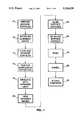
- FIG. 1is a flow diagram showing the general steps of the process of the present invention.
- FIG. 2is a diagrammatic view showing the positioning of one embodiment of alignment marks prior to superimposition.
- FIG. 3is a diagrammatic view showing the alignment marks of FIG. after superimposition.
- FIG. 4is a schematic view showing one embodiment of an infrared alignment apparatus used with the process of FIG. 1.
- FIG. 5is a schematic cross-sectional view of a monolithic CMOS device fabricated using conventional methods.
- FIG. 6is a schematic cross-sectional exploded view of the CMOS device of FIG. 5 fabricated using the process of FIG. 1.
- FIG. 7is a process flow diagram showing the fabrication of a typical CMOS device using the process of FIG. 1.
- FIG. 8is a process flow diagram showing a cross-sectional view of the fabrication of a silicon o insulator device using the process of FIG. 1.
- the present inventiongenerally comprises a process to bond surface features of silicon based materials without the use of adhesives. Atomic or crystalline bonds between the materials themselves are formed after precision alignment. This process will be referred to herein as Aligned Wafer Bonding.
- step 10the surfaces of the structures to be bonded are prepared.
- this stepwould involve polishing and cleaning the surfaces to be bonded.
- this stepwould typically involve deposition of silicon based materials such as SiO 2 , Si 3 N 4 , PtSi, TiSi 2 and polysilicon on the surfaces of the structures to be bonded as will be described in more detail herein.
- a plurality of alignment marksare established on the surfaces of the structures to be bonded.
- silicon wafers to be bondedcould be patterned with an array of orthogonal V-shaped grooves.
- V-shaped grooves 32, 34 on first and second wafers, respectively, and scribe lines 36, 38 on first and second wafers, respectivelyrepresent a patterns of alignment marks on two separate wafers which are misaligned.
- FIG. 3represents the same patterns of alignment marks after the surfaces of the wafers are aligned.
- these alignment markscould be established as surface features of separately fabricated structures.
- the surface featurescould be used for alignment purposes only, or could be the actual surface features to be bonded. This is the preferred approach since Aligned Wafer Bonding is ideally suited for bonding complementary surface features on separately fabricated structures.
- step 14the surface features to be bonded are cleaned and hydrated using conventional means. This step may be bypassed where, for example, silicide layers have been deposited during the fabrication process.
- the surface features to be bondedare positioned in direct opposition to each other so that the surfaces can be brought into contact.
- the structuresare irradiated with infrared light for viewing with an infrared imaging apparatus. This step is required so that the alignment marks can be viewed simultaneously at step 20 to resolve any misalignment then present.
- the surfacesare aligned by superimposing the alignment marks as precisely as possible, but generally within 2.5 to 5 micrometers.
- the surface features (or surfaces) of the structuresare brought into physical contact at room temperature where atomic bonding or crystalline bonding occurs naturally and without the aid of adhesives. This can be achieved by creating a partial vacuum between the surfaces of the structures. For example, hydrogen bonds are established when the surfaces of silicon wafers are brought into intimate contact. These relatively weak bonds of 10.5 kcal/mol are sufficient to hold the two wafers firmly together without relative displacement during transportation to an annealing furnace.
- the structuresare annealed at a high temperature to strengthen the bonds formed in step 26. Annealing at 950° C. for 30 min is sufficient for the formation of direct silicon bonds.
- step 30external contacts and leads are attached to the bonded structures for electrical connection to other devices.
- steps 16 through 26 of FIG. 1can be facilitated with the use of a modified Optical Associates Hyperline Model 400 Infrared Aligner, particularly where wafer surfaces are to be bonded.
- a modified Optical Associates Hyperline Model 400 Infrared Alignerparticularly where wafer surfaces are to be bonded.
- the infrared aligner 40was redesigned to hold two wafers 42, 44 with the surfaces to be bonded in a face-to-face orientation.
- a special fixturewas retrofitted to the mask plate holder 46 to allow the edges of upper wafer 42 to be held in place by partial vacuum to the upper portion of the alignment 10 column 48.
- the bottom chuck plate of the substrate holderwas replaced by an annular metal disk 50 designed to hold the lower wafer 44 under partial vacuum.
- Both upper and lower holderswere reconstructed to allow infrared radiation 52 of wavelengths in the range of 1.0 to 1.2 micrometers to pass through the wafers 42, 44 to the microscope 54 and imaging camera 56 without additional absorbing media in the optical path between the infrared light source and the microscope 54.
- the infrared aligner's rotational and translational controls 58are then used to bring the surface features of wafers 42, 44 into alignment while viewing the infrared images of the alignment marks on monitor 60.
- the vertical translational control of the bottom chuckis used to bring the focal planes of the two wafers into proximity so that an acceptably focused image of the two wafer surfaces may be viewed simultaneously.
- double sided polished silicon wafersare preferred to reduce the optical distortion caused by normal surface roughness on the backside of wafers.
- a pair of (100) oriented waferscan be patterned with an array of vertical and horizontal lines and V-shaped grooves were anisotropically etched with hot potassium hydroxide. Grooves approximately 100 micrometers wide with variable depths ranging from 10-50 micrometers have been found to provide high resolution scribe lines.
- the rotational and translation controls of infrared aligner 40would be adjusted until the V-shaped groove lines appear to be superimposed on the monitor 60.
- relative displacement of the surface features to be bondedmust be minimized or eliminated for successful Aligned Wafer Bonding.
- scanning electron microscopyis used to determine the accuracy achieved during the alignment process.
- the pixel size of 7 micrometers at 2.25 ⁇ magnification and 2 micrometers at 8.0 ⁇ magnificationis a typical limiting factor, however. It has been found that misalignment at 2.25 ⁇ magnification is on the order of 10 micrometers. This can be reduced to approximately 2.5 micrometers at 8.0 ⁇ magnification.
- the degree of alignmentcan be improved by iteratively bringing the wafers into closer proximity and adjusting the focal plane of the optical system to improve the resolution of the magnified image.
- a typical sampleis generally misaligned by less than 5 micrometers. It should also be noted that wafer flatness and surface roughness play important roles. Preferably the radius of wafer curvature should be greater than 60 meters for a 500 micrometer thick wafer with a surface microroughness of less than 10 ⁇ .
- the angle of the anisotropically etched (111) planes used as alignment marksalso directly affects the precision of alignment achieved.
- the (111) planes that define the walls of V-groovescreate a shadow image without the necessity of metal features commonly used for two sided backside alignment. Metal alignment features would be incompatible with post bonding processing.
- the (111) planes in the top wafer groovesrefract the beam creating planes in the bottom grooves totally reflect the light creating a shadow with a width equal to the horizontal projection of the inclined wall. These dark regions replicate the geometric shape of the alignment features. Planar steps in silicon or thin film insulator layers were found not to produce an acceptable image conducive to precise alignment of the wafers.
- V-grooves of at least 30 micrometers in depthare required for visual alignment of the infrared image at high magnification due to the limits o the lens magnification in present systems. Alignment accuracy is constrained by an inability to project the upper and lower surface images onto a single focal plane.
- a variety of signal processing techniquesmight improve both the image feature requirement and the resolution of the system.
- the images of each wafer planecould be independently optimized and stored electronically, then combined to reduce distortion caused by the nonidentical focal planes of the wafers.
- a high resolution infrared detector/camera and differential image processorcould be used to achieve more precise alignment.
- Aligned Wafer Bonding as heretofore describedhas many applications. Using this technique, bonded three dimensional features can be positioned within tens of nanometers vertically and within the alignment tolerance horizontally. This allows device features consistent with electronic, optical or micromechanical structures to be combined between the bonded wafers. The process will provide for viable alignment to within 5 micrometers for standard silicon wafers with surface nonuniformity less than 20 micrometers. This alignment tolerance provides several potentially useful applications of aligned bonding such as pneumatic microvalves, field emission microtriodes, and a variety of silicon based sensors. Alignment accuracies to within approximately one micrometer should be possible with the improvements in imaging described.
- One micrometer aligned bondingwould allow this technique to be applied to wafers with submicron technology since coupled features are typically not confined to the device dimensions. If we also align bond electronically communicating layers such as p-n junctions, p+or n+busses, or silicides, then three dimensional integrated circuits would be possible with Aligned Wafer Bonding. This would revolutionize integrated circuit fabrication since different sections of an integrated circuit could be separately fabricated and tested in a process optimized for each layer, then chosen by a yield map and aligned bonded together to enhance performance and yield. This process-specific approach would also apply to electrical, mechanical and optical systems and multimaterial devices such as Ge-Si and GaAs-Si, and the like. When this technique is combined with selective etch back, each new added layer could be fabricated, tested, bonded to the ensemble, and then thinned to produce a general three dimensional multilayered structure.
- Specific materials which are ideal for bonding using the process of the present inventioninclude Si, SiO 2 , Si 3 N 4 , PtSi, TiSi 2 , and polysilicon. Direct bonding of Si and SiO 2 is important in the formation of microstructures and silicon on insulator material. Si 3 N 4 can be aligned bonded as an insulating material, while PtSi, TiSi 2 , and polysilicon are temperature robust conductive materials which can be bonded as conductive materials.
- Silicides and salicidescan be bonded in the same fashion as silicon.
- the principle of this bonding techniqueis that many metal silicides tend to form SiO 2 on the surface of the material when exposed to an oxidizing ambient.
- a very thin SiO 2 layeris formed on the surface of the silicide by exposing the surface to a chemically oxidizing substance. This forms a very thin layer of SiO 2 which is sufficient to promote bonding but thin enough not to impair the electrical conduction across the bonded interface. This has been accomplished for PtSi and TiSi 2 , and should apply to a variety of other silicides.
- the bondforms at room temperature and requires a high temperature anneal as is the case with silicon bonding.
- a bondcan be formed by fusing silicon to metal to form a metal silicide and in the process bonding the wafers together.
- metal silicidesform at temperatures as low as 175° C. for Pd 2 Si or as low as 350° C. for Ta-Si. This would be advantageous for bonding wafers which are restricted in temperature by organics or metals such as Aluminum when bonded.
- a problem that requires attentionis that unless a room temperature prebond can be made, the alignment would have to take place at the final bond temperature.
- PtSi and TiSi 2 bondingdepends upon the principle of the formation of a hydrophilic layer on the surface of the material by exposing it to an oxidizing ambient. A very thin layer of SiO 2 forms on the surface and then allows direct wafer bonding to be accomplished. Once annealed, the bond forms a strong highly conductive connection between the materials. This bond is used as the principle mechanical and electrical connection between aligned bonded wafers of CMOS, Bi-CMOS, and other electrically interconnected structures.
- PtSi direct bondingfollows. Silicon substrates, 3 inches in diameter, boron doped at 10 ⁇ cm, (100) orientation, are cleaned and etched in dilute HF prior to loading in an e-beam chamber. Pt is evaporated onto the substrates held at 350° C. where silicidation immediately occurs on deposition. The vacuum at deposition was 10 -6 torr. A total thickness of 60 ⁇ PtSi is thereby formed on the substrates. The resistivity of the film is approximately 30 ⁇ cm. The wafers are then slightly etched in a 60° C. aqua regia solution of 3:1, HCl:HNO 3 ; this selectively etches Pt leaving only PtSi.
- the wafersAfter cleaning in base and acid baths, the wafers are rinsed and dried in a spin dryer.
- the cleaning agentsnormally create a thin oxide layer on silicon and some silicide surfaces, and the silicide surface is uniformly hydrophilic after the cleaning process.
- the hydrophilic surfaceis necessary but not a sufficient condition for the direct bonding process.
- the wafersare then brought into intimate contact where initial hydrogen bonds are formed. Bonding is established at room temperature for PtSi to PtSi surfaces and PtSi surfaces to hydrophilic silicon wafers in the form of relatively weak water hydrogen bonds of 10.5 kcal/mol. The bonds, however, are sufficient to hold the two wafers firmly together without relative displacement during the transport to the annealing furnace.
- the wafer pairsare then annealed at 700° C. in an N 2 ambient for 2 hours to form direct silicide bonds.
- the bonding reactionis the same as for silicon or silicon dioxide surfaces as previously described.
- aluminumis evaporated on both sides of the bonded PtSi-PtSi coated silicon wafer for metal contact.
- the coated wafersare then annealed at 450° C. in a forming gas of Ar+4% H 2 for 30 minutes.
- the TiSi 2can be deposited on the wafer by cosputtering titanium and silicon followed by a silicidation process.
- polysilicon to polysilicon bondingpolysilicon can be prepared by low pressure chemical vapor deposition followed by a phosphorus diffusion process. In each case, a cohesive bond for each of the deposited materials can be accomplished after 2 hours annealing at 900° C. in an inert ambient.
- Aligned Wafer Bondinglends itself to fabrication of a variety of electrical, mechanical, and optical devices.
- a p-channel MOS wafercan be align bonded to a n-channel MOS wafer to produce a vertical CMOS device.
- Thisoffers the advantage that the n- and p- channel wafers are fabricated separately, thus reducing process complexity, and providing a technology which is dielectrically isolated and totally latch up free.
- FIG. 5there is shown a schematic cross-sectional view of a monolithic CMOS invertor fabricated using conventional N-well technology.
- FIG. 6shows a device with the same function but which is fabricated using the process of the present invention.
- the conductive bonding micropads 62, 64are selectively align-bonded between the prefabricated wafers. TiSi 2 or PtSi is used as the interconnect and bonding agent between the wafers.
- the unbonded surfacesare covered with a PECVD Si 3 N 4 prior to align bonding steps to serve as a passivation layer.
- the bonding micropadsare fabricated onto field oxide regions where silicide fusion bonding takes place.
- steps 66 through 80schematically show p- and n- MOS processing steps which are conventional, but which include special attention to polysilicon etching and recessed gate pads 86, 88 imbedded in the field oxide.
- the processed p- and n- wafersthen receive appropriate surface treatments for aligned bonding as shown in steps 82 and 84.
- CMOS devicesAn extension of align-bonded CMOS devices is the fabrication of align-bonded Bi-CMOS devices.
- a CMOS device with exposed contact studs made of either a metal silicide or other refractory conductor forming a planewould be align bonded to a bipolar wafer with associated conductive studs.
- the CMOS and/or bipolar technologiescould be independently optimized as desired.
- An examplewould be an SOI CMOS structure. The structure would then be a three layer structure which is thinned after each wafer is added.
- Another embodimentwould be to align bond a CMOS wafer to a bipolar wafer where the conductive pads form the mechanical and electrical connection between the circuitry in the same manner as the n- and p- mos are align bonded in the CMOS case.
- a further extensionwould be to use Aligned Wafer Bonding to fabricate integrated analog to digital devices, high power to low power devices, and the like. Aligned Wafer Bonding would be particularly suited for this application since the individual devices are the products of dissimilar processes and do not lend themselves to monolithic fabrication.
- a planar conductive bonding surfacewould be formed by a patterned layer of a metal silicide, refractory metal, or polysilicon which forms contacts between the wafers and mechanically bonds the structures.
- npn and pnp bipolar transistorsIn the case of integrated bipolar devices, it is generally difficult to fabricate monolithic npn and pnp bipolar transistors of high gain or speed on a single chip of semiconductor material. This is because the base width and doping for either npn or pnp transistors must be carefully controlled to achieve high gain or speed. It is relatively straightforward to control the fabrication of either a p-type base in an npn or an n-type base in a pnp transistor, but very difficult to achieve both in a single process sequence. By separately fabricating the npn and pnp portions of the structures, each transistor type can be optimized prior to integration by aligned wafer bonding.
- Integrated microsensorsis another application of aligned wafer bonding. While it is often that case that microsensors and integrated circuits are made from the same materials, the specific processes and economics of the microsensors and integrated circuits are so different that their integration onto a common substrate is not practical. Microsensor and integrated circuit technologies can be combined by providing a patterned conductive plane on each to electrically interconnect and mechanically bond the circuitry to the microsensors with aligned wafer bonding. Similarly, microactuators such as gears and switches could be combined with electronic circuitry monolithically included in the overall design of a specific function. As is the case with microsensor technologies, the specific processes and economics of microactuator and integrated circuit technologies do not blend well into an integrated monolithic technology. The process of the present invention can be used to integrate these technologies after separate fabrication and optimization. Photonic technologies can also be bonded in this manner.
- a silicon-on-insulator (SOI) structurecan be fabricated using Aligned Wafer Bonding.
- Steps 90 through 94show the conventional process for preparing an insulator handle.
- an insulator handle 110is prepared.
- a layer 106 of SiO 2is deposited on the insulator handle 110 to act serve as a bonding intermediate.
- Si 3 N 4is pattern deposited to serve as polish stops 108.
- the silicon based device 112 of step 98is Align Wafer Bonded to the layer 106 of SiO 2 , to form the silicon-on-insulator structure of step 102.
- the device 112is thinned to the level of the polish stops 108.
- this inventionprovides for the fabrication of complex integrated devices that could include mechanical, electronic and/or optical elements formed in separate prefabricated layers.
Landscapes
- Engineering & Computer Science (AREA)
- Physics & Mathematics (AREA)
- Condensed Matter Physics & Semiconductors (AREA)
- General Physics & Mathematics (AREA)
- Computer Hardware Design (AREA)
- Microelectronics & Electronic Packaging (AREA)
- Power Engineering (AREA)
- Manufacturing & Machinery (AREA)
- Element Separation (AREA)
Abstract
Description
Claims (23)
Priority Applications (1)
| Application Number | Priority Date | Filing Date | Title |
|---|---|---|---|
| US07/883,583US5236118A (en) | 1992-05-12 | 1992-05-12 | Aligned wafer bonding |
Applications Claiming Priority (1)
| Application Number | Priority Date | Filing Date | Title |
|---|---|---|---|
| US07/883,583US5236118A (en) | 1992-05-12 | 1992-05-12 | Aligned wafer bonding |
Publications (1)
| Publication Number | Publication Date |
|---|---|
| US5236118Atrue US5236118A (en) | 1993-08-17 |
Family
ID=25382894
Family Applications (1)
| Application Number | Title | Priority Date | Filing Date |
|---|---|---|---|
| US07/883,583Expired - LifetimeUS5236118A (en) | 1992-05-12 | 1992-05-12 | Aligned wafer bonding |
Country Status (1)
| Country | Link |
|---|---|
| US (1) | US5236118A (en) |
Cited By (121)
| Publication number | Priority date | Publication date | Assignee | Title |
|---|---|---|---|---|
| US5427973A (en)* | 1992-05-25 | 1995-06-27 | Sony Corporation | Method for production of SOI transistor device having a storage cell |
| US5504026A (en)* | 1995-04-14 | 1996-04-02 | Analog Devices, Inc. | Methods for planarization and encapsulation of micromechanical devices in semiconductor processes |
| WO1996013060A1 (en)* | 1994-10-24 | 1996-05-02 | Daimler-Benz Aktiengesellschaft | Method for directly connecting flat bodies and articles produced according to said method from said flat bodies |
| DE4445348A1 (en)* | 1994-12-20 | 1996-06-27 | Daimler Benz Ag | Directly connecting planar bodies, substrate and contact plates |
| US5659195A (en)* | 1995-06-08 | 1997-08-19 | The Regents Of The University Of California | CMOS integrated microsensor with a precision measurement circuit |
| FR2748159A1 (en)* | 1996-04-27 | 1997-10-31 | Bosch Gmbh Robert | PROCESS FOR MANUFACTURING SEMICONDUCTOR ELEMENTS HAVING MICROMECHANICAL STRUCTURES |
| US5783477A (en)* | 1996-09-20 | 1998-07-21 | Hewlett-Packard Company | Method for bonding compounds semiconductor wafers to create an ohmic interface |
| US5792943A (en)* | 1997-04-30 | 1998-08-11 | Hewlett-Packard Company | Planar separation column for use in sample analysis system |
| US5806181A (en)* | 1993-11-16 | 1998-09-15 | Formfactor, Inc. | Contact carriers (tiles) for populating larger substrates with spring contacts |
| US5825195A (en)* | 1992-06-10 | 1998-10-20 | Micron Technology, Inc. | Method and apparatus for testing an unpackaged semiconductor die |
| US5829667A (en)* | 1995-12-23 | 1998-11-03 | International Business Machines Corporation | Method for strengthening a solder joint when attaching integrated circuits to printed circuit boards |
| US5888390A (en)* | 1997-04-30 | 1999-03-30 | Hewlett-Packard Company | Multilayer integrated assembly for effecting fluid handling functions |
| US5915167A (en)* | 1997-04-04 | 1999-06-22 | Elm Technology Corporation | Three dimensional structure memory |
| US5932048A (en)* | 1995-04-06 | 1999-08-03 | Komatsu Electronic Metals Co., Ltd. | Method of fabricating direct-bonded semiconductor wafers |
| US5935430A (en)* | 1997-04-30 | 1999-08-10 | Hewlett-Packard Company | Structure for capturing express transient liquid phase during diffusion bonding of planar devices |
| US5946553A (en)* | 1991-06-04 | 1999-08-31 | Micron Technology, Inc. | Process for manufacturing a semiconductor package with bi-substrate die |
| US5985693A (en)* | 1994-09-30 | 1999-11-16 | Elm Technology Corporation | High density three-dimensional IC interconnection |
| US5994152A (en) | 1996-02-21 | 1999-11-30 | Formfactor, Inc. | Fabricating interconnects and tips using sacrificial substrates |
| US5997708A (en)* | 1997-04-30 | 1999-12-07 | Hewlett-Packard Company | Multilayer integrated assembly having specialized intermediary substrate |
| US6008113A (en)* | 1998-05-19 | 1999-12-28 | Kavlico Corporation | Process for wafer bonding in a vacuum |
| US6043134A (en)* | 1998-08-28 | 2000-03-28 | Micron Technology, Inc. | Semiconductor wafer alignment processes |
| US6079276A (en) | 1995-02-28 | 2000-06-27 | Rosemount Inc. | Sintered pressure sensor for a pressure transmitter |
| US6085967A (en)* | 1998-12-28 | 2000-07-11 | Eastman Kodak Company | Method of registrably aligning fabricated wafers preceding bonding |
| US6158712A (en)* | 1998-10-16 | 2000-12-12 | Agilent Technologies, Inc. | Multilayer integrated assembly having an integral microminiature valve |
| US6168971B1 (en) | 1998-05-05 | 2001-01-02 | Fujitsu Limited | Method of assembling thin film jumper connectors to a substrate |
| US6171972B1 (en) | 1998-03-17 | 2001-01-09 | Rosemount Aerospace Inc. | Fracture-resistant micromachined devices |
| US6198159B1 (en)* | 1997-03-28 | 2001-03-06 | Ube Industries, Ltd. | Bonded wafer, process for producing same and substrate |
| US6225154B1 (en) | 1993-07-27 | 2001-05-01 | Hyundai Electronics America | Bonding of silicon wafers |
| US6242817B1 (en) | 1998-12-28 | 2001-06-05 | Eastman Kodak Company | Fabricated wafer for integration in a wafer structure |
| US6440832B1 (en)* | 2001-07-06 | 2002-08-27 | Advanced Micro Devices, Inc. | Hybrid MOS and schottky gate technology |
| US20020119597A1 (en)* | 2001-01-30 | 2002-08-29 | Stmicroelectronics S.R.L. | Process for sealing and connecting parts of electromechanical, fluid and optical microsystems and device obtained thereby |
| US6484585B1 (en) | 1995-02-28 | 2002-11-26 | Rosemount Inc. | Pressure sensor for a pressure transmitter |
| US6505516B1 (en) | 2000-01-06 | 2003-01-14 | Rosemount Inc. | Capacitive pressure sensing with moving dielectric |
| US6508129B1 (en) | 2000-01-06 | 2003-01-21 | Rosemount Inc. | Pressure sensor capsule with improved isolation |
| US6516671B2 (en) | 2000-01-06 | 2003-02-11 | Rosemount Inc. | Grain growth of electrical interconnection for microelectromechanical systems (MEMS) |
| US6520020B1 (en) | 2000-01-06 | 2003-02-18 | Rosemount Inc. | Method and apparatus for a direct bonded isolated pressure sensor |
| US20030042626A1 (en)* | 2001-08-30 | 2003-03-06 | Howarth James J. | Method of ball grid array (BGA) alignment, method of testing, alignment apparatus and semiconductor device assembly |
| US6534381B2 (en)* | 1999-01-08 | 2003-03-18 | Silicon Genesis Corporation | Method for fabricating multi-layered substrates |
| US6551857B2 (en) | 1997-04-04 | 2003-04-22 | Elm Technology Corporation | Three dimensional structure integrated circuits |
| US6561038B2 (en) | 2000-01-06 | 2003-05-13 | Rosemount Inc. | Sensor with fluid isolation barrier |
| US20030124327A1 (en)* | 2002-01-03 | 2003-07-03 | International Business Machines Corporation | Hybrid substrate and method for fabricating the same |
| US6610582B1 (en)* | 2002-03-26 | 2003-08-26 | Northrop Grumman Corporation | Field-assisted fusion bonding |
| US20030193076A1 (en)* | 2002-04-11 | 2003-10-16 | Robert Patti | Interlocking conductor method for bonding wafers to produce stacked integrated circuits |
| US6640415B2 (en) | 1999-06-07 | 2003-11-04 | Formfactor, Inc. | Segmented contactor |
| US6682981B2 (en) | 1992-04-08 | 2004-01-27 | Elm Technology Corporation | Stress controlled dielectric integrated circuit fabrication |
| US6690185B1 (en) | 1997-01-15 | 2004-02-10 | Formfactor, Inc. | Large contactor with multiple, aligned contactor units |
| US6741085B1 (en) | 1993-11-16 | 2004-05-25 | Formfactor, Inc. | Contact carriers (tiles) for populating larger substrates with spring contacts |
| US20040126994A1 (en)* | 2002-12-31 | 2004-07-01 | Rafael Reif | Method of forming a multi-layer semiconductor structure having a seamless bonding interface |
| US20040188500A1 (en)* | 2003-03-31 | 2004-09-30 | Litton Systems, Inc. | Bonding method for microchannel plates |
| US20040219765A1 (en)* | 2002-12-31 | 2004-11-04 | Rafael Reif | Method of forming a multi-layer semiconductor structure incorporating a processing handle member |
| US6821826B1 (en)* | 2003-09-30 | 2004-11-23 | International Business Machines Corporation | Three dimensional CMOS integrated circuits having device layers built on different crystal oriented wafers |
| US6836003B2 (en) | 1997-09-15 | 2004-12-28 | Micron Technology, Inc. | Integrated circuit package alignment feature |
| US20050013019A1 (en)* | 2003-07-18 | 2005-01-20 | Asia Pacific Microsystems, Inc. | Method of maintaining photolithographic precision alignment after wafer bonding process |
| US6848316B2 (en) | 2002-05-08 | 2005-02-01 | Rosemount Inc. | Pressure sensor assembly |
| US20050091843A1 (en)* | 2003-10-31 | 2005-05-05 | Honeywell International, Inc. | Vibrating beam accelerometer two-wafer fabrication process |
| EP1278245A4 (en)* | 2000-04-28 | 2005-06-15 | Sumitomo Mitsubishi Silicon | Method and apparatus for producing bonded dielectric separation wafer |
| US20050255666A1 (en)* | 2004-05-11 | 2005-11-17 | Miradia Inc. | Method and structure for aligning mechanical based device to integrated circuits |
| US20060139643A1 (en)* | 2004-12-28 | 2006-06-29 | Industrial Technology Research Institute | Alignment method of using alignment marks on wafer edge |
| US20060292744A1 (en)* | 1999-10-01 | 2006-12-28 | Ziptronix | Three dimensional device integration method and integrated device |
| US7176545B2 (en) | 1992-04-08 | 2007-02-13 | Elm Technology Corporation | Apparatus and methods for maskless pattern generation |
| US20070119812A1 (en)* | 2005-11-28 | 2007-05-31 | Sebastien Kerdiles | Process and equipment for bonding by molecular adhesion |
| US20070126445A1 (en)* | 2005-11-30 | 2007-06-07 | Micron Technology, Inc. | Integrated circuit package testing devices and methods of making and using same |
| US20070191070A1 (en)* | 1996-12-16 | 2007-08-16 | Rao Raman K | Reconfigurable mobile device interfaces supporting authenticated high-quality video, audio, TV and multimedia services |
| US7302982B2 (en) | 2001-04-11 | 2007-12-04 | Avery Dennison Corporation | Label applicator and system |
| US20080083818A1 (en)* | 2006-10-06 | 2008-04-10 | Asml Netherlands B.V. | Measuring the bonding of bonded substrates |
| US7402897B2 (en) | 2002-08-08 | 2008-07-22 | Elm Technology Corporation | Vertical system integration |
| US20080191310A1 (en)* | 2007-02-12 | 2008-08-14 | Weng-Jin Wu | By-product removal for wafer bonding process |
| US20090079084A1 (en)* | 2007-09-24 | 2009-03-26 | Research Triangle Institute | Preventing breakage of long metal signal conductors on semiconductor substrates |
| US20090079056A1 (en)* | 2007-09-25 | 2009-03-26 | Rti International | Large substrate structural vias |
| US20090090950A1 (en)* | 2007-10-05 | 2009-04-09 | Micron Technology, Inc. | Semiconductor devices |
| US7601039B2 (en) | 1993-11-16 | 2009-10-13 | Formfactor, Inc. | Microelectronic contact structure and method of making same |
| US20090267183A1 (en)* | 2008-04-28 | 2009-10-29 | Research Triangle Institute | Through-substrate power-conducting via with embedded capacitance |
| US20090298207A1 (en)* | 2004-02-13 | 2009-12-03 | Erich Thallner | Method for bonding wafers |
| US20100020397A1 (en)* | 2008-07-28 | 2010-01-28 | Canon Kabushiki Kaisha | Method for producing optical element and the optical element |
| US20100054092A1 (en)* | 2006-11-10 | 2010-03-04 | Eta Sa Manufacture Horlogere Suisse | Method of manufacturing multi-level, silicon, micromechanical parts and parts thereby obtained |
| US20100068868A1 (en)* | 2008-09-18 | 2010-03-18 | Samsung Electronics Co., Ltd. | Wafer temporary bonding method using silicon direct bonding |
| US7682933B1 (en)* | 2007-09-26 | 2010-03-23 | The United States Of America As Represented By The Secretary Of The Air Force | Wafer alignment and bonding |
| US20100187665A1 (en)* | 2009-01-26 | 2010-07-29 | Sixis, Inc. | Integral metal structure with conductive post portions |
| US20110008632A1 (en)* | 2009-07-10 | 2011-01-13 | Seagate Technology Llc | Self-aligned wafer bonding |
| US7927975B2 (en) | 2009-02-04 | 2011-04-19 | Micron Technology, Inc. | Semiconductor material manufacture |
| US20110127581A1 (en)* | 2009-12-01 | 2011-06-02 | Bethoux Jean-Marc | Heterostructure for electronic power components, optoelectronic or photovoltaic components |
| US20110168434A1 (en)* | 2010-01-12 | 2011-07-14 | International Business Machines Corporation | Bonded structure employing metal semiconductor alloy bonding |
| US20110189820A1 (en)* | 2010-02-04 | 2011-08-04 | Headway Technologies, Inc. | Method of manufacturing layered chip package |
| US8033838B2 (en) | 1996-02-21 | 2011-10-11 | Formfactor, Inc. | Microelectronic contact structure |
| US8373428B2 (en) | 1993-11-16 | 2013-02-12 | Formfactor, Inc. | Probe card assembly and kit, and methods of making same |
| US8440472B2 (en)* | 2004-01-07 | 2013-05-14 | Nikon Corporation | Stacking apparatus and method for stacking integrated circuit elements |
| WO2013097894A1 (en)* | 2011-12-28 | 2013-07-04 | Ev Group E. Thallner Gmbh | Method and device for bonding of substrates |
| WO2013152176A1 (en)* | 2012-04-04 | 2013-10-10 | Massachusetts Institute Of Technology | Monolithic integration of cmos and non-silicon devices |
| DE102012107899A1 (en)* | 2012-04-25 | 2013-10-31 | Taiwan Semiconductor Manufacturing Co., Ltd. | Wafer assembly for use during manufacturing integrated switching circuits, has integrated circuits formed on process and carrier wafers bonded to process wafer, and adhesive layer bonding wafers, where carrier wafer includes alignment mark |
| US8603862B2 (en) | 2010-05-14 | 2013-12-10 | International Business Machines Corporation | Precise-aligned lock-and-key bonding structures |
| US20140356983A1 (en)* | 2013-06-03 | 2014-12-04 | International Business Machines Corporation | Distorting donor wafer to corresponding distortion of host wafer |
| US9082627B2 (en) | 2000-02-16 | 2015-07-14 | Ziptronix, Inc. | Method for low temperature bonding and bonded structure |
| US9111982B2 (en) | 2012-04-25 | 2015-08-18 | Taiwan Semiconductor Manufacturing Company, Ltd. | Wafer assembly with carrier wafer |
| US9300645B1 (en) | 2013-03-14 | 2016-03-29 | Ip Holdings, Inc. | Mobile IO input and output for smartphones, tablet, and wireless devices including touch screen, voice, pen, and gestures |
| US9466538B1 (en)* | 2015-11-25 | 2016-10-11 | Globalfoundries Inc. | Method to achieve ultra-high chip-to-chip alignment accuracy for wafer-to-wafer bonding process |
| US10434749B2 (en) | 2003-05-19 | 2019-10-08 | Invensas Bonding Technologies, Inc. | Method of room temperature covalent bonding |
| US10490414B2 (en) | 2016-06-28 | 2019-11-26 | Taiwan Semiconductor Manufacturing Co., Ltd. | Pattern transfer technique and method of manufacturing the same |
| CN111081629A (en)* | 2019-11-04 | 2020-04-28 | 武汉大学 | Alignment mark fabrication method and cavity position determination method for SOI wafer with cavity |
| US10840205B2 (en) | 2017-09-24 | 2020-11-17 | Invensas Bonding Technologies, Inc. | Chemical mechanical polishing for hybrid bonding |
| US11011418B2 (en) | 2005-08-11 | 2021-05-18 | Invensas Bonding Technologies, Inc. | 3D IC method and device |
| US11011494B2 (en) | 2018-08-31 | 2021-05-18 | Invensas Bonding Technologies, Inc. | Layer structures for making direct metal-to-metal bonds at low temperatures in microelectronics |
| US11158573B2 (en) | 2018-10-22 | 2021-10-26 | Invensas Bonding Technologies, Inc. | Interconnect structures |
| US11244920B2 (en) | 2018-12-18 | 2022-02-08 | Invensas Bonding Technologies, Inc. | Method and structures for low temperature device bonding |
| US11264345B2 (en) | 2015-08-25 | 2022-03-01 | Invensas Bonding Technologies, Inc. | Conductive barrier direct hybrid bonding |
| US11393779B2 (en) | 2018-06-13 | 2022-07-19 | Invensas Bonding Technologies, Inc. | Large metal pads over TSV |
| US20220359293A1 (en)* | 2019-12-30 | 2022-11-10 | Soitec | Method for producing a composite structure comprising a thin monocristalline layer on a carrier substrate |
| US11515279B2 (en) | 2018-04-11 | 2022-11-29 | Adeia Semiconductor Bonding Technologies Inc. | Low temperature bonded structures |
| US11710718B2 (en) | 2015-07-10 | 2023-07-25 | Adeia Semiconductor Technologies Llc | Structures and methods for low temperature bonding using nanoparticles |
| US11728313B2 (en) | 2018-06-13 | 2023-08-15 | Adeia Semiconductor Bonding Technologies Inc. | Offset pads over TSV |
| US11735523B2 (en) | 2020-05-19 | 2023-08-22 | Adeia Semiconductor Bonding Technologies Inc. | Laterally unconfined structure |
| US11804377B2 (en) | 2018-04-05 | 2023-10-31 | Adeia Semiconductor Bonding Technologies, Inc. | Method for preparing a surface for direct-bonding |
| US11894326B2 (en) | 2017-03-17 | 2024-02-06 | Adeia Semiconductor Bonding Technologies Inc. | Multi-metal contact structure |
| US11908739B2 (en) | 2017-06-05 | 2024-02-20 | Adeia Semiconductor Technologies Llc | Flat metal features for microelectronics applications |
| US11929347B2 (en) | 2020-10-20 | 2024-03-12 | Adeia Semiconductor Technologies Llc | Mixed exposure for large die |
| US11955454B2 (en)* | 2021-10-25 | 2024-04-09 | Yangtze Memory Technologies Co., Ltd. | Wafer bonding apparatus and method |
| US11973056B2 (en) | 2016-10-27 | 2024-04-30 | Adeia Semiconductor Technologies Llc | Methods for low temperature bonding using nanoparticles |
| US12100676B2 (en) | 2018-04-11 | 2024-09-24 | Adeia Semiconductor Bonding Technologies Inc. | Low temperature bonded structures |
| CN119330301A (en)* | 2024-12-19 | 2025-01-21 | 苏州芯镁信电子科技有限公司 | A MEMS micromirror and a method for preparing the same |
| US12211809B2 (en) | 2020-12-30 | 2025-01-28 | Adeia Semiconductor Bonding Technologies Inc. | Structure with conductive feature and method of forming same |
| US12381128B2 (en) | 2020-12-28 | 2025-08-05 | Adeia Semiconductor Bonding Technologies Inc. | Structures with through-substrate vias and methods for forming the same |
| US12424584B2 (en) | 2020-10-29 | 2025-09-23 | Adeia Semiconductor Bonding Technologies Inc. | Direct bonding methods and structures |
Citations (3)
| Publication number | Priority date | Publication date | Assignee | Title |
|---|---|---|---|---|
| US4700466A (en)* | 1985-02-08 | 1987-10-20 | Kabushiki Kaisha Toshiba | Method of manufacturing semiconductor device wherein silicon substrates are bonded together |
| US4771016A (en)* | 1987-04-24 | 1988-09-13 | Harris Corporation | Using a rapid thermal process for manufacturing a wafer bonded soi semiconductor |
| US4939101A (en)* | 1988-09-06 | 1990-07-03 | General Electric Company | Method of making direct bonded wafers having a void free interface |
- 1992
- 1992-05-12USUS07/883,583patent/US5236118A/ennot_activeExpired - Lifetime
Patent Citations (3)
| Publication number | Priority date | Publication date | Assignee | Title |
|---|---|---|---|---|
| US4700466A (en)* | 1985-02-08 | 1987-10-20 | Kabushiki Kaisha Toshiba | Method of manufacturing semiconductor device wherein silicon substrates are bonded together |
| US4771016A (en)* | 1987-04-24 | 1988-09-13 | Harris Corporation | Using a rapid thermal process for manufacturing a wafer bonded soi semiconductor |
| US4939101A (en)* | 1988-09-06 | 1990-07-03 | General Electric Company | Method of making direct bonded wafers having a void free interface |
Non-Patent Citations (29)
| Title |
|---|
| Advertisements and product brochures by Karl Suss America, Inc.* |
| Bower, et al., "Silicon Nitride Direct Bonding", Electric Letters, Apr. 18, 1990. |
| Bower, et al., Silicon Nitride Direct Bonding , Electric Letters, Apr. 18, 1990.* |
| Hayashi, et al., Fabrication of Three Dimensional IC Using Cumulatively Bonded IC (CUBIC) Technology Symposium on VLSI Technology, Hawaii, 1990.* |
| Hayashi, et al., Fabrication of Three-Dimensional IC Using Cumulatively Bonded IC (CUBIC) Technology Symposium on VLSI Technology, Hawaii, 1990. |
| Hirata et al., "Silicon Diaphragm Pressure Sensors Fabricated by Anodic Oxidation Etch Stop", Sensors and Actuators, 1990. |
| Hirata et al., Silicon Diaphragm Pressure Sensors Fabricated by Anodic Oxidation Etch Stop , Sensors and Actuators, 1990.* |
| Lasky, J. B., "Wafer Bonding for Silicon-On-Insulator Technologies" Appl. Phys. Lett. Jan. 6, 1986. |
| Lasky, J. B., Wafer Bonding for Silicon On Insulator Technologies Appl. Phys. Lett. Jan. 6, 1986.* |
| Little, et al., "The 3-D Computer", IEEE International Conference on Wafer Scale Integration, San Francisco, CA 1989. |
| Little, et al., The 3 D Computer , IEEE International Conference on Wafer Scale Integration, San Francisco, CA 1989.* |
| Petersen, et al., "Silicon Fusion Bonding for Pressure Sensors", Solid-State Sensor and Actuator Workshop Technical Digest, Hilton Head Island, S.C., 1988. |
| Petersen, et al., Silicon Fusion Bonding for Pressure Sensors , Solid State Sensor and Actuator Workshop Technical Digest, Hilton Head Island, S.C., 1988.* |
| Petersen, Kurt E., "Fabrication of an Integrated, Planar, Silicon Ink-Jet Structure" IEEE Transactions on Electric Devices, Nov. 1979. |
| Petersen, Kurt E., Fabrication of an Integrated, Planar, Silicon Ink Jet Structure IEEE Transactions on Electric Devices, Nov. 1979.* |
| Smith, et al., "A Wafer-to-Wafer Alignment Technique", Sensors and Actuators, 1989. |
| Smith, et al., "The Design and Fabrication of a Magnetically Aucuated Micromachined Flow Valve", Sensors and Actuators, 1990. |
| Smith, et al., A Wafer to Wafer Alignment Technique , Sensors and Actuators, 1989.* |
| Smith, et al., Micromechanical Packaging for Chemical Microsensor s, IEEE Transactions on Electron Devices, Jun. 1988.* |
| Smith, et al., Micromechanical Packaging for Chemical Microsensor's, IEEE Transactions on Electron Devices, Jun. 1988. |
| Smith, et al., The Design and Fabrication of a Magnetically Aucuated Micromachined Flow Valve , Sensors and Actuators, 1990.* |
| Stemme, "A CMOS Integrated Silicon Gas-Flow Sensor with Pulse-Modulated Out-Put" presented at Fourth International Con. On Solid-State Sensors and Actuators, Tokyo, Japan, Jun. 2-5, 1987. |
| Stemme, A CMOS Integrated Silicon Gas Flow Sensor with Pulse Modulated Out Put presented at Fourth International Con. On Solid State Sensors and Actuators, Tokyo, Japan, Jun. 2 5, 1987.* |
| Stengl, et al., "A Model for the Silicon Wafer Bonding Process", Jpn. J. Appl. Phys., 1989. |
| Stengl, et al., A Model for the Silicon Wafer Bonding Process , Jpn. J. Appl. Phys., 1989.* |
| Tenrez, et al., "Silicon Microcavities Fabricated with a new Technique", Electronic Letters, Apr. 18, 1986. |
| Tenrez, et al., Silicon Microcavities Fabricated with a new Technique , Electronic Letters, Apr. 18, 1986.* |
| Yasumoto, et al., "Promising New Fabrication Process Developed for Stacked LSI's" Technical Digest in IEEE Int. Electron Devices Mtg. Dec. 1984. |
| Yasumoto, et al., Promising New Fabrication Process Developed for Stacked LSI s Technical Digest in IEEE Int. Electron Devices Mtg. Dec. 1984.* |
Cited By (276)
| Publication number | Priority date | Publication date | Assignee | Title |
|---|---|---|---|---|
| US5946553A (en)* | 1991-06-04 | 1999-08-31 | Micron Technology, Inc. | Process for manufacturing a semiconductor package with bi-substrate die |
| US7307020B2 (en) | 1992-04-08 | 2007-12-11 | Elm Technology Corporation | Membrane 3D IC fabrication |
| US7670893B2 (en) | 1992-04-08 | 2010-03-02 | Taiwan Semiconductor Manufacturing Co., Ltd. | Membrane IC fabrication |
| US7385835B2 (en) | 1992-04-08 | 2008-06-10 | Elm Technology Corporation | Membrane 3D IC fabrication |
| US7763948B2 (en) | 1992-04-08 | 2010-07-27 | Taiwan Semiconductor Manufacturing Co., Ltd. | Flexible and elastic dielectric integrated circuit |
| US7550805B2 (en) | 1992-04-08 | 2009-06-23 | Elm Technology Corporation | Stress-controlled dielectric integrated circuit |
| US7485571B2 (en) | 1992-04-08 | 2009-02-03 | Elm Technology Corporation | Method of making an integrated circuit |
| US6682981B2 (en) | 1992-04-08 | 2004-01-27 | Elm Technology Corporation | Stress controlled dielectric integrated circuit fabrication |
| US7176545B2 (en) | 1992-04-08 | 2007-02-13 | Elm Technology Corporation | Apparatus and methods for maskless pattern generation |
| US6765279B2 (en) | 1992-04-08 | 2004-07-20 | Elm Technology Corporation | Membrane 3D IC fabrication |
| US7479694B2 (en) | 1992-04-08 | 2009-01-20 | Elm Technology Corporation | Membrane 3D IC fabrication |
| US20040150068A1 (en)* | 1992-04-08 | 2004-08-05 | Elm Technology Corporation | Membrane 3D IC fabrication |
| US7820469B2 (en) | 1992-04-08 | 2010-10-26 | Taiwan Semiconductor Manufacturing Co., Ltd. | Stress-controlled dielectric integrated circuit |
| US7223696B2 (en) | 1992-04-08 | 2007-05-29 | Elm Technology Corporation | Methods for maskless lithography |
| US7911012B2 (en) | 1992-04-08 | 2011-03-22 | Taiwan Semiconductor Manufacturing Co., Ltd. | Flexible and elastic dielectric integrated circuit |
| US6713327B2 (en) | 1992-04-08 | 2004-03-30 | Elm Technology Corporation | Stress controlled dielectric integrated circuit fabrication |
| US7242012B2 (en) | 1992-04-08 | 2007-07-10 | Elm Technology Corporation | Lithography device for semiconductor circuit pattern generator |
| US7615837B2 (en) | 1992-04-08 | 2009-11-10 | Taiwan Semiconductor Manufacturing Company | Lithography device for semiconductor circuit pattern generation |
| US5478782A (en)* | 1992-05-25 | 1995-12-26 | Sony Corporation | Method bonding for production of SOI transistor device |
| US5427973A (en)* | 1992-05-25 | 1995-06-27 | Sony Corporation | Method for production of SOI transistor device having a storage cell |
| US5523254A (en)* | 1992-05-25 | 1996-06-04 | Sony Corporation | Method for production of SOI transistor device and SOI transistor |
| US5825195A (en)* | 1992-06-10 | 1998-10-20 | Micron Technology, Inc. | Method and apparatus for testing an unpackaged semiconductor die |
| US6570221B1 (en) | 1993-07-27 | 2003-05-27 | Hyundai Electronics America | Bonding of silicon wafers |
| US6225154B1 (en) | 1993-07-27 | 2001-05-01 | Hyundai Electronics America | Bonding of silicon wafers |
| US20080231305A1 (en)* | 1993-11-16 | 2008-09-25 | Formfactor, Inc. | Contact carriers (tiles) for populating larger substrates with spring contacts |
| US5806181A (en)* | 1993-11-16 | 1998-09-15 | Formfactor, Inc. | Contact carriers (tiles) for populating larger substrates with spring contacts |
| US8373428B2 (en) | 1993-11-16 | 2013-02-12 | Formfactor, Inc. | Probe card assembly and kit, and methods of making same |
| US7347702B2 (en) | 1993-11-16 | 2008-03-25 | Formfactor, Inc. | Contact carriers (tiles) for populating larger substrates with spring contacts |
| US7714598B2 (en) | 1993-11-16 | 2010-05-11 | Formfactor, Inc. | Contact carriers (tiles) for populating larger substrates with spring contacts |
| US20040163252A1 (en)* | 1993-11-16 | 2004-08-26 | Formfactor, Inc. | Contact carriers (tiles) for populating larger substrates with spring contacts |
| US7601039B2 (en) | 1993-11-16 | 2009-10-13 | Formfactor, Inc. | Microelectronic contact structure and method of making same |
| US6741085B1 (en) | 1993-11-16 | 2004-05-25 | Formfactor, Inc. | Contact carriers (tiles) for populating larger substrates with spring contacts |
| US7140883B2 (en) | 1993-11-16 | 2006-11-28 | Formfactor, Inc. | Contact carriers (tiles) for populating larger substrates with spring contacts |
| US20070075715A1 (en)* | 1993-11-16 | 2007-04-05 | Formfactor, Inc. | Contact Carriers (Tiles) For Populating Larger Substrates With Spring Contacts |
| US5985693A (en)* | 1994-09-30 | 1999-11-16 | Elm Technology Corporation | High density three-dimensional IC interconnection |
| WO1996013060A1 (en)* | 1994-10-24 | 1996-05-02 | Daimler-Benz Aktiengesellschaft | Method for directly connecting flat bodies and articles produced according to said method from said flat bodies |
| DE4445348A1 (en)* | 1994-12-20 | 1996-06-27 | Daimler Benz Ag | Directly connecting planar bodies, substrate and contact plates |
| US6082199A (en) | 1995-02-28 | 2000-07-04 | Rosemount Inc. | Pressure sensor cavity etched with hot POCL3 gas |
| US6484585B1 (en) | 1995-02-28 | 2002-11-26 | Rosemount Inc. | Pressure sensor for a pressure transmitter |
| US6089097A (en) | 1995-02-28 | 2000-07-18 | Rosemount Inc. | Elongated pressure sensor for a pressure transmitter |
| US6079276A (en) | 1995-02-28 | 2000-06-27 | Rosemount Inc. | Sintered pressure sensor for a pressure transmitter |
| US5932048A (en)* | 1995-04-06 | 1999-08-03 | Komatsu Electronic Metals Co., Ltd. | Method of fabricating direct-bonded semiconductor wafers |
| US5504026A (en)* | 1995-04-14 | 1996-04-02 | Analog Devices, Inc. | Methods for planarization and encapsulation of micromechanical devices in semiconductor processes |
| US5659195A (en)* | 1995-06-08 | 1997-08-19 | The Regents Of The University Of California | CMOS integrated microsensor with a precision measurement circuit |
| US5829667A (en)* | 1995-12-23 | 1998-11-03 | International Business Machines Corporation | Method for strengthening a solder joint when attaching integrated circuits to printed circuit boards |
| US5994152A (en) | 1996-02-21 | 1999-11-30 | Formfactor, Inc. | Fabricating interconnects and tips using sacrificial substrates |
| US8033838B2 (en) | 1996-02-21 | 2011-10-11 | Formfactor, Inc. | Microelectronic contact structure |
| FR2748159A1 (en)* | 1996-04-27 | 1997-10-31 | Bosch Gmbh Robert | PROCESS FOR MANUFACTURING SEMICONDUCTOR ELEMENTS HAVING MICROMECHANICAL STRUCTURES |
| US5783477A (en)* | 1996-09-20 | 1998-07-21 | Hewlett-Packard Company | Method for bonding compounds semiconductor wafers to create an ohmic interface |
| US20070191070A1 (en)* | 1996-12-16 | 2007-08-16 | Rao Raman K | Reconfigurable mobile device interfaces supporting authenticated high-quality video, audio, TV and multimedia services |
| US6690185B1 (en) | 1997-01-15 | 2004-02-10 | Formfactor, Inc. | Large contactor with multiple, aligned contactor units |
| US6198159B1 (en)* | 1997-03-28 | 2001-03-06 | Ube Industries, Ltd. | Bonded wafer, process for producing same and substrate |
| US8318538B2 (en) | 1997-04-04 | 2012-11-27 | Elm Technology Corp. | Three dimensional structure memory |
| US8824159B2 (en) | 1997-04-04 | 2014-09-02 | Glenn J. Leedy | Three dimensional structure memory |
| US6551857B2 (en) | 1997-04-04 | 2003-04-22 | Elm Technology Corporation | Three dimensional structure integrated circuits |
| US8796862B2 (en) | 1997-04-04 | 2014-08-05 | Glenn J Leedy | Three dimensional memory structure |
| US8288206B2 (en) | 1997-04-04 | 2012-10-16 | Elm Technology Corp | Three dimensional structure memory |
| US8791581B2 (en) | 1997-04-04 | 2014-07-29 | Glenn J Leedy | Three dimensional structure memory |
| US8629542B2 (en) | 1997-04-04 | 2014-01-14 | Glenn J. Leedy | Three dimensional structure memory |
| US6208545B1 (en) | 1997-04-04 | 2001-03-27 | Glenn J. Leedy | Three dimensional structure memory |
| US8410617B2 (en) | 1997-04-04 | 2013-04-02 | Elm Technology | Three dimensional structure memory |
| US8035233B2 (en) | 1997-04-04 | 2011-10-11 | Elm Technology Corporation | Adjacent substantially flexible substrates having integrated circuits that are bonded together by non-polymeric layer |
| US7504732B2 (en) | 1997-04-04 | 2009-03-17 | Elm Technology Corporation | Three dimensional structure memory |
| US6133640A (en)* | 1997-04-04 | 2000-10-17 | Elm Technology Corporation | Three-dimensional structure memory |
| US9087556B2 (en) | 1997-04-04 | 2015-07-21 | Glenn J Leedy | Three dimension structure memory |
| US8933570B2 (en) | 1997-04-04 | 2015-01-13 | Elm Technology Corp. | Three dimensional structure memory |
| US8928119B2 (en) | 1997-04-04 | 2015-01-06 | Glenn J. Leedy | Three dimensional structure memory |
| US6632706B1 (en) | 1997-04-04 | 2003-10-14 | Elm Technology Corporation | Three dimensional structure integrated circuit fabrication process |
| US8841778B2 (en) | 1997-04-04 | 2014-09-23 | Glenn J Leedy | Three dimensional memory structure |
| US5915167A (en)* | 1997-04-04 | 1999-06-22 | Elm Technology Corporation | Three dimensional structure memory |
| US7705466B2 (en) | 1997-04-04 | 2010-04-27 | Elm Technology Corporation | Three dimensional multi layer memory and control logic integrated circuit structure |
| US8907499B2 (en) | 1997-04-04 | 2014-12-09 | Glenn J Leedy | Three dimensional structure memory |
| US7138295B2 (en) | 1997-04-04 | 2006-11-21 | Elm Technology Corporation | Method of information processing using three dimensional integrated circuits |
| US7193239B2 (en) | 1997-04-04 | 2007-03-20 | Elm Technology Corporation | Three dimensional structure integrated circuit |
| US7474004B2 (en) | 1997-04-04 | 2009-01-06 | Elm Technology Corporation | Three dimensional structure memory |
| US9401183B2 (en) | 1997-04-04 | 2016-07-26 | Glenn J. Leedy | Stacked integrated memory device |
| US6563224B2 (en) | 1997-04-04 | 2003-05-13 | Elm Technology Corporation | Three dimensional structure integrated circuit |
| US5792943A (en)* | 1997-04-30 | 1998-08-11 | Hewlett-Packard Company | Planar separation column for use in sample analysis system |
| US5888390A (en)* | 1997-04-30 | 1999-03-30 | Hewlett-Packard Company | Multilayer integrated assembly for effecting fluid handling functions |
| US5935430A (en)* | 1997-04-30 | 1999-08-10 | Hewlett-Packard Company | Structure for capturing express transient liquid phase during diffusion bonding of planar devices |
| US5997708A (en)* | 1997-04-30 | 1999-12-07 | Hewlett-Packard Company | Multilayer integrated assembly having specialized intermediary substrate |
| US6836003B2 (en) | 1997-09-15 | 2004-12-28 | Micron Technology, Inc. | Integrated circuit package alignment feature |
| US6858453B1 (en) | 1997-09-15 | 2005-02-22 | Micron Technology, Inc. | Integrated circuit package alignment feature |
| US6171972B1 (en) | 1998-03-17 | 2001-01-09 | Rosemount Aerospace Inc. | Fracture-resistant micromachined devices |
| US6168971B1 (en) | 1998-05-05 | 2001-01-02 | Fujitsu Limited | Method of assembling thin film jumper connectors to a substrate |
| US6008113A (en)* | 1998-05-19 | 1999-12-28 | Kavlico Corporation | Process for wafer bonding in a vacuum |
| WO1999060607A3 (en)* | 1998-05-19 | 2000-05-04 | Kavlico Corp | Tool for wafer bonding in a vacuum |
| US6043134A (en)* | 1998-08-28 | 2000-03-28 | Micron Technology, Inc. | Semiconductor wafer alignment processes |
| US6158712A (en)* | 1998-10-16 | 2000-12-12 | Agilent Technologies, Inc. | Multilayer integrated assembly having an integral microminiature valve |
| US6242817B1 (en) | 1998-12-28 | 2001-06-05 | Eastman Kodak Company | Fabricated wafer for integration in a wafer structure |
| US6085967A (en)* | 1998-12-28 | 2000-07-11 | Eastman Kodak Company | Method of registrably aligning fabricated wafers preceding bonding |
| US6534381B2 (en)* | 1999-01-08 | 2003-03-18 | Silicon Genesis Corporation | Method for fabricating multi-layered substrates |
| US7578057B2 (en) | 1999-06-07 | 2009-08-25 | Formfactor, Inc. | Method of fabricating segmented contactor |
| US20040058487A1 (en)* | 1999-06-07 | 2004-03-25 | Formfactor, Inc. | Segmented contactor |
| US7065870B2 (en) | 1999-06-07 | 2006-06-27 | Formfactor, Inc. | Segmented contactor |
| US20100043226A1 (en)* | 1999-06-07 | 2010-02-25 | Formfactor, Inc. | Segmented contactor |
| US6640415B2 (en) | 1999-06-07 | 2003-11-04 | Formfactor, Inc. | Segmented contactor |
| US7215131B1 (en) | 1999-06-07 | 2007-05-08 | Formfactor, Inc. | Segmented contactor |
| US8011089B2 (en) | 1999-06-07 | 2011-09-06 | Formfactor, Inc. | Method of repairing segmented contactor |
| US9431368B2 (en) | 1999-10-01 | 2016-08-30 | Ziptronix, Inc. | Three dimensional device integration method and integrated device |
| US9564414B2 (en) | 1999-10-01 | 2017-02-07 | Ziptronix, Inc. | Three dimensional device integration method and integrated device |
| US10366962B2 (en) | 1999-10-01 | 2019-07-30 | Invensas Bonding Technologies, Inc. | Three dimensional device integration method and integrated device |
| US20060292744A1 (en)* | 1999-10-01 | 2006-12-28 | Ziptronix | Three dimensional device integration method and integrated device |
| US6516671B2 (en) | 2000-01-06 | 2003-02-11 | Rosemount Inc. | Grain growth of electrical interconnection for microelectromechanical systems (MEMS) |
| US6520020B1 (en) | 2000-01-06 | 2003-02-18 | Rosemount Inc. | Method and apparatus for a direct bonded isolated pressure sensor |
| US6561038B2 (en) | 2000-01-06 | 2003-05-13 | Rosemount Inc. | Sensor with fluid isolation barrier |
| US6505516B1 (en) | 2000-01-06 | 2003-01-14 | Rosemount Inc. | Capacitive pressure sensing with moving dielectric |
| US6508129B1 (en) | 2000-01-06 | 2003-01-21 | Rosemount Inc. | Pressure sensor capsule with improved isolation |
| US9082627B2 (en) | 2000-02-16 | 2015-07-14 | Ziptronix, Inc. | Method for low temperature bonding and bonded structure |
| US9331149B2 (en) | 2000-02-16 | 2016-05-03 | Ziptronix, Inc. | Method for low temperature bonding and bonded structure |
| US10312217B2 (en) | 2000-02-16 | 2019-06-04 | Invensas Bonding Technologies, Inc. | Method for low temperature bonding and bonded structure |
| US9391143B2 (en) | 2000-02-16 | 2016-07-12 | Ziptronix, Inc. | Method for low temperature bonding and bonded structure |
| EP1278245A4 (en)* | 2000-04-28 | 2005-06-15 | Sumitomo Mitsubishi Silicon | Method and apparatus for producing bonded dielectric separation wafer |
| US7531897B2 (en)* | 2001-01-30 | 2009-05-12 | Stmicroelectronics S.R.L. | Process for sealing and connecting parts of electromechanical, fluid and optical microsystems and device obtained thereby |
| US8050011B2 (en) | 2001-01-30 | 2011-11-01 | Stmicroelectronics S.R.L. | Process for sealing and connecting parts of electromechanical, fluid and optical microsystems and device obtained thereby |
| US20090186447A1 (en)* | 2001-01-30 | 2009-07-23 | Stmicroelectronics S.R.I. | Process for sealing and connecting parts of electromechanical, fluid and optical microsystems and device obtained thereby |
| US20020119597A1 (en)* | 2001-01-30 | 2002-08-29 | Stmicroelectronics S.R.L. | Process for sealing and connecting parts of electromechanical, fluid and optical microsystems and device obtained thereby |
| US7302982B2 (en) | 2001-04-11 | 2007-12-04 | Avery Dennison Corporation | Label applicator and system |
| US6440832B1 (en)* | 2001-07-06 | 2002-08-27 | Advanced Micro Devices, Inc. | Hybrid MOS and schottky gate technology |
| US20030042626A1 (en)* | 2001-08-30 | 2003-03-06 | Howarth James J. | Method of ball grid array (BGA) alignment, method of testing, alignment apparatus and semiconductor device assembly |
| US6963143B2 (en) | 2001-08-30 | 2005-11-08 | Micron Technology, Inc. | Method of ball grid array (BGA) alignment, method of testing, alignment apparatus and semiconductor device assembly |
| US7005754B2 (en)* | 2001-08-30 | 2006-02-28 | Micron Technology, Inc. | Method of ball grid array (BGA) alignment, method of testing, alignment apparatus and semiconductor device assembly |
| US6991960B2 (en) | 2001-08-30 | 2006-01-31 | Micron Technology, Inc. | Method of semiconductor device package alignment and method of testing |
| US20030094707A1 (en)* | 2001-08-30 | 2003-05-22 | Howarth James J. | Method of ball grid array (BGA) alignment, method of testing, alignment apparatus and semiconductor device assembly |
| US20030094706A1 (en)* | 2001-08-30 | 2003-05-22 | Howarth James J. | Method of ball grid array (BGA) alignment, method of testing, alignment apparatus and semiconductor device assembly |
| US20030124327A1 (en)* | 2002-01-03 | 2003-07-03 | International Business Machines Corporation | Hybrid substrate and method for fabricating the same |
| US6994903B2 (en)* | 2002-01-03 | 2006-02-07 | International Business Machines Corp. | Hybrid substrate and method for fabricating the same |
| US6610582B1 (en)* | 2002-03-26 | 2003-08-26 | Northrop Grumman Corporation | Field-assisted fusion bonding |
| US6642081B1 (en)* | 2002-04-11 | 2003-11-04 | Robert Patti | Interlocking conductor method for bonding wafers to produce stacked integrated circuits |
| US20030193076A1 (en)* | 2002-04-11 | 2003-10-16 | Robert Patti | Interlocking conductor method for bonding wafers to produce stacked integrated circuits |
| US6848316B2 (en) | 2002-05-08 | 2005-02-01 | Rosemount Inc. | Pressure sensor assembly |
| US7402897B2 (en) | 2002-08-08 | 2008-07-22 | Elm Technology Corporation | Vertical system integration |
| US8080442B2 (en) | 2002-08-08 | 2011-12-20 | Elm Technology Corporation | Vertical system integration |
| US8269327B2 (en) | 2002-08-08 | 2012-09-18 | Glenn J Leedy | Vertical system integration |
| US8587102B2 (en) | 2002-08-08 | 2013-11-19 | Glenn J Leedy | Vertical system integration |
| US20040126994A1 (en)* | 2002-12-31 | 2004-07-01 | Rafael Reif | Method of forming a multi-layer semiconductor structure having a seamless bonding interface |
| US7064055B2 (en) | 2002-12-31 | 2006-06-20 | Massachusetts Institute Of Technology | Method of forming a multi-layer semiconductor structure having a seamless bonding interface |
| US20060099796A1 (en)* | 2002-12-31 | 2006-05-11 | Rafael Reif | Method of forming a multi-layer semiconductor structure having a seam-less bonding interface |
| US20060087019A1 (en)* | 2002-12-31 | 2006-04-27 | Rafael Reif | Multi-layer integrated semiconductor structure having an electrical shielding portion |
| US7067909B2 (en) | 2002-12-31 | 2006-06-27 | Massachusetts Institute Of Technology | Multi-layer integrated semiconductor structure having an electrical shielding portion |
| WO2004061952A3 (en)* | 2002-12-31 | 2005-05-19 | Massachusetts Inst Technology | Method of forming a multi-layer semiconductor structure having a seamless bonding interface |
| US20040219765A1 (en)* | 2002-12-31 | 2004-11-04 | Rafael Reif | Method of forming a multi-layer semiconductor structure incorporating a processing handle member |
| US7307003B2 (en) | 2002-12-31 | 2007-12-11 | Massachusetts Institute Of Technology | Method of forming a multi-layer semiconductor structure incorporating a processing handle member |
| WO2004092785A3 (en)* | 2003-03-31 | 2004-12-09 | Litton Systems Inc | Bonding method for microchannel plates |
| US6874674B2 (en)* | 2003-03-31 | 2005-04-05 | Litton Systems, Inc. | Bonding method for microchannel plates |
| US20040188500A1 (en)* | 2003-03-31 | 2004-09-30 | Litton Systems, Inc. | Bonding method for microchannel plates |
| US11760059B2 (en) | 2003-05-19 | 2023-09-19 | Adeia Semiconductor Bonding Technologies Inc. | Method of room temperature covalent bonding |
| US10434749B2 (en) | 2003-05-19 | 2019-10-08 | Invensas Bonding Technologies, Inc. | Method of room temperature covalent bonding |
| US6967145B2 (en)* | 2003-07-18 | 2005-11-22 | Asia Pacific Microsystems, Inc. | Method of maintaining photolithographic precision alignment after wafer bonding process |
| US20050013019A1 (en)* | 2003-07-18 | 2005-01-20 | Asia Pacific Microsystems, Inc. | Method of maintaining photolithographic precision alignment after wafer bonding process |
| US6821826B1 (en)* | 2003-09-30 | 2004-11-23 | International Business Machines Corporation | Three dimensional CMOS integrated circuits having device layers built on different crystal oriented wafers |
| US20050067620A1 (en)* | 2003-09-30 | 2005-03-31 | International Business Machines Corporation | Three dimensional CMOS integrated circuits having device layers built on different crystal oriented wafers |
| US7024934B2 (en) | 2003-10-31 | 2006-04-11 | Honeywell International, Inc. | Vibrating beam accelerometer |
| US6938334B2 (en)* | 2003-10-31 | 2005-09-06 | Honeywell International, Inc. | Vibrating beam accelerometer two-wafer fabrication process |
| US20050160816A1 (en)* | 2003-10-31 | 2005-07-28 | Honeywell International, Inc. | Vibrating beam accelerometer |
| US20050091843A1 (en)* | 2003-10-31 | 2005-05-05 | Honeywell International, Inc. | Vibrating beam accelerometer two-wafer fabrication process |
| US9105675B2 (en) | 2004-01-07 | 2015-08-11 | Nikon Corporation | WH (wafer-holder) process |
| US8735180B2 (en) | 2004-01-07 | 2014-05-27 | Nikon Corporation | Multiple-points measurement |
| US8440472B2 (en)* | 2004-01-07 | 2013-05-14 | Nikon Corporation | Stacking apparatus and method for stacking integrated circuit elements |
| US20090298207A1 (en)* | 2004-02-13 | 2009-12-03 | Erich Thallner | Method for bonding wafers |
| US7998833B2 (en)* | 2004-02-13 | 2011-08-16 | Erich Thallner | Method for bonding wafers |
| US20050255666A1 (en)* | 2004-05-11 | 2005-11-17 | Miradia Inc. | Method and structure for aligning mechanical based device to integrated circuits |
| US7390723B2 (en)* | 2004-12-28 | 2008-06-24 | Industrial Technology Research Institute | Alignment method of using alignment marks on wafer edge |
| US20060139643A1 (en)* | 2004-12-28 | 2006-06-29 | Industrial Technology Research Institute | Alignment method of using alignment marks on wafer edge |
| US11011418B2 (en) | 2005-08-11 | 2021-05-18 | Invensas Bonding Technologies, Inc. | 3D IC method and device |
| US11289372B2 (en) | 2005-08-11 | 2022-03-29 | Invensas Bonding Technologies, Inc. | 3D IC method and device |
| US11515202B2 (en) | 2005-08-11 | 2022-11-29 | Adeia Semiconductor Bonding Technologies Inc. | 3D IC method and device |
| US8091601B2 (en) | 2005-11-28 | 2012-01-10 | S.O.I.Tec Silicon On Insulator Technologies | Equipment for bonding by molecular adhesion |
| US20090261064A1 (en)* | 2005-11-28 | 2009-10-22 | S.O.I.Tec Silicon On Insulator Technologies | Process for bonding by molecular adhesion |
| US7601271B2 (en) | 2005-11-28 | 2009-10-13 | S.O.I.Tec Silicon On Insulator Technologies | Process and equipment for bonding by molecular adhesion |
| US20090294072A1 (en)* | 2005-11-28 | 2009-12-03 | S.O.I.Tec Silicon On Insulator Technologies | Equipment for bonding by molecular adhesion |
| US20070119812A1 (en)* | 2005-11-28 | 2007-05-31 | Sebastien Kerdiles | Process and equipment for bonding by molecular adhesion |
| US8158013B2 (en) | 2005-11-28 | 2012-04-17 | Soitec | Process for bonding by molecular adhesion |
| US20070126445A1 (en)* | 2005-11-30 | 2007-06-07 | Micron Technology, Inc. | Integrated circuit package testing devices and methods of making and using same |
| US20080083818A1 (en)* | 2006-10-06 | 2008-04-10 | Asml Netherlands B.V. | Measuring the bonding of bonded substrates |
| US20100054092A1 (en)* | 2006-11-10 | 2010-03-04 | Eta Sa Manufacture Horlogere Suisse | Method of manufacturing multi-level, silicon, micromechanical parts and parts thereby obtained |
| US8501584B2 (en)* | 2006-11-10 | 2013-08-06 | Eta Sa Manufacture Horlogère Suisse | Method of manufacturing multi-level, silicon, micromechanical parts and parts thereby obtained |
| US20080191310A1 (en)* | 2007-02-12 | 2008-08-14 | Weng-Jin Wu | By-product removal for wafer bonding process |
| US8222086B2 (en) | 2007-09-24 | 2012-07-17 | Research Triangle Institute | Integrated semiconductor substrate structure using incompatible processes |
| US7829994B2 (en) | 2007-09-24 | 2010-11-09 | Sixis, Inc. | Semiconductor substrate elastomeric stack |
| US20110183469A1 (en)* | 2007-09-24 | 2011-07-28 | Research Triangle Institute | Integrated semiconductor substrate structure using incompatible processes |
| US20090080152A1 (en)* | 2007-09-24 | 2009-03-26 | Research Triangle Institute | Stackable self-aligning insulative guide tray for holding semiconductor substrates |
| US7944041B2 (en)* | 2007-09-24 | 2011-05-17 | Research Triangle Institute | Integrated semiconductor substrate structure using incompatible processes |
| US20090079058A1 (en)* | 2007-09-24 | 2009-03-26 | Research Triangle Institute | Semiconductor substrate elastomeric stack |
| US7831874B2 (en)* | 2007-09-24 | 2010-11-09 | Sixis, Inc. | Local defect memories on semiconductor substrates in a stack computer |
| US8404585B2 (en) | 2007-09-24 | 2013-03-26 | Research Triangle Institute | Preventing breakage of long metal signal conductors on semiconductor substrates |
| US20090079463A1 (en)* | 2007-09-24 | 2009-03-26 | Research Triangle Institute | Local defect memories on semiconductor substrates in a stack computer |
| US20090079059A1 (en)* | 2007-09-24 | 2009-03-26 | Research Triangle Institute | Integrated semiconductor substrate structure using incompatible processes |
| US7999388B2 (en) | 2007-09-24 | 2011-08-16 | Research Triangle Institute | Preventing breakage of long metal signal conductors on semiconductor substrates |
| US7719844B2 (en) | 2007-09-24 | 2010-05-18 | Sixis, Inc. | Stackable self-aligning insulative guide tray for holding semiconductor substrates |
| US20090080158A1 (en)* | 2007-09-24 | 2009-03-26 | Research Triangle Institute | Comb-shaped power bus bar assembly structure having integrated capacitors |
| US20090079084A1 (en)* | 2007-09-24 | 2009-03-26 | Research Triangle Institute | Preventing breakage of long metal signal conductors on semiconductor substrates |
| US7764498B2 (en) | 2007-09-24 | 2010-07-27 | Sixis, Inc. | Comb-shaped power bus bar assembly structure having integrated capacitors |
| US20090079056A1 (en)* | 2007-09-25 | 2009-03-26 | Rti International | Large substrate structural vias |
| US20100200540A1 (en)* | 2007-09-25 | 2010-08-12 | Sixis, Inc. | Large substrate structural vias |
| US7709966B2 (en) | 2007-09-25 | 2010-05-04 | Sixis, Inc. | Large substrate structural vias |
| US8008134B2 (en) | 2007-09-25 | 2011-08-30 | Research Triangle Institute | Large substrate structural vias |
| US7682933B1 (en)* | 2007-09-26 | 2010-03-23 | The United States Of America As Represented By The Secretary Of The Air Force | Wafer alignment and bonding |
| US7875529B2 (en)* | 2007-10-05 | 2011-01-25 | Micron Technology, Inc. | Semiconductor devices |
| US20090090950A1 (en)* | 2007-10-05 | 2009-04-09 | Micron Technology, Inc. | Semiconductor devices |
| US20090267183A1 (en)* | 2008-04-28 | 2009-10-29 | Research Triangle Institute | Through-substrate power-conducting via with embedded capacitance |
| US20100020397A1 (en)* | 2008-07-28 | 2010-01-28 | Canon Kabushiki Kaisha | Method for producing optical element and the optical element |
| US8305686B2 (en)* | 2008-07-28 | 2012-11-06 | Canon Kabushiki Kaisha | Method for producing optical element and the optical element |
| US20100068868A1 (en)* | 2008-09-18 | 2010-03-18 | Samsung Electronics Co., Ltd. | Wafer temporary bonding method using silicon direct bonding |
| US8343851B2 (en)* | 2008-09-18 | 2013-01-01 | Samsung Electronics Co., Ltd. | Wafer temporary bonding method using silicon direct bonding |
| US20100187665A1 (en)* | 2009-01-26 | 2010-07-29 | Sixis, Inc. | Integral metal structure with conductive post portions |
| US8129834B2 (en) | 2009-01-26 | 2012-03-06 | Research Triangle Institute | Integral metal structure with conductive post portions |
| US7927975B2 (en) | 2009-02-04 | 2011-04-19 | Micron Technology, Inc. | Semiconductor material manufacture |
| US8389385B2 (en) | 2009-02-04 | 2013-03-05 | Micron Technology, Inc. | Semiconductor material manufacture |
| US20110008632A1 (en)* | 2009-07-10 | 2011-01-13 | Seagate Technology Llc | Self-aligned wafer bonding |
| US8460794B2 (en) | 2009-07-10 | 2013-06-11 | Seagate Technology Llc | Self-aligned wafer bonding |
| US8784975B2 (en) | 2009-07-10 | 2014-07-22 | Seagate Technology Llc | Self-aligned wafer bonding |
| US8759881B2 (en) | 2009-12-01 | 2014-06-24 | Soitec | Heterostructure for electronic power components, optoelectronic or photovoltaic components |
| US20110127581A1 (en)* | 2009-12-01 | 2011-06-02 | Bethoux Jean-Marc | Heterostructure for electronic power components, optoelectronic or photovoltaic components |
| US8841777B2 (en) | 2010-01-12 | 2014-09-23 | International Business Machines Corporation | Bonded structure employing metal semiconductor alloy bonding |
| US20110168434A1 (en)* | 2010-01-12 | 2011-07-14 | International Business Machines Corporation | Bonded structure employing metal semiconductor alloy bonding |
| US9214388B2 (en) | 2010-01-12 | 2015-12-15 | International Business Machines Corporation | Bonded structure employing metal semiconductor alloy bonding |
| US8012802B2 (en)* | 2010-02-04 | 2011-09-06 | Headway Technologies, Inc. | Method of manufacturing layered chip package |
| US20110189820A1 (en)* | 2010-02-04 | 2011-08-04 | Headway Technologies, Inc. | Method of manufacturing layered chip package |
| US8603862B2 (en) | 2010-05-14 | 2013-12-10 | International Business Machines Corporation | Precise-aligned lock-and-key bonding structures |
| WO2013097894A1 (en)* | 2011-12-28 | 2013-07-04 | Ev Group E. Thallner Gmbh | Method and device for bonding of substrates |
| US9530763B2 (en) | 2012-04-04 | 2016-12-27 | Massachusetts Institute Of Technology | Monolithic integration of CMOS and non-silicon devices |
| WO2013152176A1 (en)* | 2012-04-04 | 2013-10-10 | Massachusetts Institute Of Technology | Monolithic integration of cmos and non-silicon devices |
| EP2834850A4 (en)* | 2012-04-04 | 2015-09-30 | Massachusetts Inst Technology | MONOLITHIC INTEGRATION OF CMOS AND NON-SILICON DEVICES |
| DE102012107899B4 (en)* | 2012-04-25 | 2014-07-17 | Taiwan Semiconductor Manufacturing Co., Ltd. | Wafer assembly with carrier wafer and manufacturing method therefor |
| US9601324B2 (en) | 2012-04-25 | 2017-03-21 | Taiwan Semiconductor Manufacturing Company, Ltd. | Method of making wafer assembly |
| DE102012107899A1 (en)* | 2012-04-25 | 2013-10-31 | Taiwan Semiconductor Manufacturing Co., Ltd. | Wafer assembly for use during manufacturing integrated switching circuits, has integrated circuits formed on process and carrier wafers bonded to process wafer, and adhesive layer bonding wafers, where carrier wafer includes alignment mark |
| US9111982B2 (en) | 2012-04-25 | 2015-08-18 | Taiwan Semiconductor Manufacturing Company, Ltd. | Wafer assembly with carrier wafer |
| US9300645B1 (en) | 2013-03-14 | 2016-03-29 | Ip Holdings, Inc. | Mobile IO input and output for smartphones, tablet, and wireless devices including touch screen, voice, pen, and gestures |
| US20140356983A1 (en)* | 2013-06-03 | 2014-12-04 | International Business Machines Corporation | Distorting donor wafer to corresponding distortion of host wafer |
| US9058974B2 (en)* | 2013-06-03 | 2015-06-16 | International Business Machines Corporation | Distorting donor wafer to corresponding distortion of host wafer |
| US11710718B2 (en) | 2015-07-10 | 2023-07-25 | Adeia Semiconductor Technologies Llc | Structures and methods for low temperature bonding using nanoparticles |
| US12381168B2 (en) | 2015-08-25 | 2025-08-05 | Adeia Semiconductor Bonding Technologies Inc. | Conductive barrier direct hybrid bonding |
| US11830838B2 (en) | 2015-08-25 | 2023-11-28 | Adeia Semiconductor Bonding Technologies Inc. | Conductive barrier direct hybrid bonding |
| US11264345B2 (en) | 2015-08-25 | 2022-03-01 | Invensas Bonding Technologies, Inc. | Conductive barrier direct hybrid bonding |
| US9466538B1 (en)* | 2015-11-25 | 2016-10-11 | Globalfoundries Inc. | Method to achieve ultra-high chip-to-chip alignment accuracy for wafer-to-wafer bonding process |
| US10490414B2 (en) | 2016-06-28 | 2019-11-26 | Taiwan Semiconductor Manufacturing Co., Ltd. | Pattern transfer technique and method of manufacturing the same |
| US11289341B2 (en) | 2016-06-28 | 2022-03-29 | Taiwan Semiconductor Manufacturing Company, Ltd. | Pattern transfer technique and method of manufacturing the same |
| US12027487B2 (en) | 2016-10-27 | 2024-07-02 | Adeia Semiconductor Technologies Llc | Structures for low temperature bonding using nanoparticles |
| US11973056B2 (en) | 2016-10-27 | 2024-04-30 | Adeia Semiconductor Technologies Llc | Methods for low temperature bonding using nanoparticles |
| US11894326B2 (en) | 2017-03-17 | 2024-02-06 | Adeia Semiconductor Bonding Technologies Inc. | Multi-metal contact structure |
| US11908739B2 (en) | 2017-06-05 | 2024-02-20 | Adeia Semiconductor Technologies Llc | Flat metal features for microelectronics applications |
| US12381173B2 (en) | 2017-09-24 | 2025-08-05 | Adeia Semiconductor Bonding Technologies Inc. | Direct hybrid bonding of substrates having microelectronic components with different profiles and/or pitches at the bonding interface |
| US10840205B2 (en) | 2017-09-24 | 2020-11-17 | Invensas Bonding Technologies, Inc. | Chemical mechanical polishing for hybrid bonding |
| US11552041B2 (en) | 2017-09-24 | 2023-01-10 | Adeia Semiconductor Bonding Technologies Inc. | Chemical mechanical polishing for hybrid bonding |
| US11804377B2 (en) | 2018-04-05 | 2023-10-31 | Adeia Semiconductor Bonding Technologies, Inc. | Method for preparing a surface for direct-bonding |
| US12341018B2 (en) | 2018-04-05 | 2025-06-24 | Adeia Semiconductor Bonding Technologies Inc. | Method for preparing a surface for direct-bonding |
| US12132020B2 (en) | 2018-04-11 | 2024-10-29 | Adeia Semiconductor Bonding Technologies Inc. | Low temperature bonded structures |
| US12046571B2 (en) | 2018-04-11 | 2024-07-23 | Adeia Semiconductor Bonding Technologies Inc. | Low temperature bonded structures |
| US12100676B2 (en) | 2018-04-11 | 2024-09-24 | Adeia Semiconductor Bonding Technologies Inc. | Low temperature bonded structures |
| US11515279B2 (en) | 2018-04-11 | 2022-11-29 | Adeia Semiconductor Bonding Technologies Inc. | Low temperature bonded structures |
| US12205926B2 (en) | 2018-06-13 | 2025-01-21 | Adeia Semiconductor Bonding Technologies Inc. | TSV as pad |
| US11749645B2 (en) | 2018-06-13 | 2023-09-05 | Adeia Semiconductor Bonding Technologies Inc. | TSV as pad |
| US12243851B2 (en) | 2018-06-13 | 2025-03-04 | Adeia Semiconductor Bonding Technologies Inc. | Offset pads over TSV |
| US11728313B2 (en) | 2018-06-13 | 2023-08-15 | Adeia Semiconductor Bonding Technologies Inc. | Offset pads over TSV |
| US11955445B2 (en) | 2018-06-13 | 2024-04-09 | Adeia Semiconductor Bonding Technologies Inc. | Metal pads over TSV |
| US11393779B2 (en) | 2018-06-13 | 2022-07-19 | Invensas Bonding Technologies, Inc. | Large metal pads over TSV |
| US12136605B2 (en) | 2018-08-31 | 2024-11-05 | Adeia Semiconductor Bonding Technologies Inc. | Layer structures for making direct metal-to-metal bonds at low temperatures in microelectronics and method for forming the same |
| US11011494B2 (en) | 2018-08-31 | 2021-05-18 | Invensas Bonding Technologies, Inc. | Layer structures for making direct metal-to-metal bonds at low temperatures in microelectronics |
| US11756880B2 (en) | 2018-10-22 | 2023-09-12 | Adeia Semiconductor Bonding Technologies Inc. | Interconnect structures |
| US12125784B2 (en) | 2018-10-22 | 2024-10-22 | Adeia Semiconductor Bonding Technologies Inc. | Interconnect structures |
| US11158573B2 (en) | 2018-10-22 | 2021-10-26 | Invensas Bonding Technologies, Inc. | Interconnect structures |
| US12154880B2 (en) | 2018-12-18 | 2024-11-26 | Adeia Semiconductor Bonding Technologies Inc. | Method and structures for low temperature device bonding |
| US11244920B2 (en) | 2018-12-18 | 2022-02-08 | Invensas Bonding Technologies, Inc. | Method and structures for low temperature device bonding |
| CN111081629A (en)* | 2019-11-04 | 2020-04-28 | 武汉大学 | Alignment mark fabrication method and cavity position determination method for SOI wafer with cavity |
| CN111081629B (en)* | 2019-11-04 | 2022-08-16 | 宁波华彰企业管理合伙企业(有限合伙) | Method for manufacturing alignment mark of SOI wafer with cavity and method for determining cavity position |
| US20220359293A1 (en)* | 2019-12-30 | 2022-11-10 | Soitec | Method for producing a composite structure comprising a thin monocristalline layer on a carrier substrate |
| US12087631B2 (en)* | 2019-12-30 | 2024-09-10 | Soitec | Method for producing a composite structure comprising a thin monocristalline layer on a carrier substrate |
| US11735523B2 (en) | 2020-05-19 | 2023-08-22 | Adeia Semiconductor Bonding Technologies Inc. | Laterally unconfined structure |
| US12033943B2 (en) | 2020-05-19 | 2024-07-09 | Adeia Semiconductor Bonding Technologies Inc. | Laterally unconfined structure |
| US11929347B2 (en) | 2020-10-20 | 2024-03-12 | Adeia Semiconductor Technologies Llc | Mixed exposure for large die |
| US12424584B2 (en) | 2020-10-29 | 2025-09-23 | Adeia Semiconductor Bonding Technologies Inc. | Direct bonding methods and structures |
| US12381128B2 (en) | 2020-12-28 | 2025-08-05 | Adeia Semiconductor Bonding Technologies Inc. | Structures with through-substrate vias and methods for forming the same |
| US12211809B2 (en) | 2020-12-30 | 2025-01-28 | Adeia Semiconductor Bonding Technologies Inc. | Structure with conductive feature and method of forming same |
| US11955454B2 (en)* | 2021-10-25 | 2024-04-09 | Yangtze Memory Technologies Co., Ltd. | Wafer bonding apparatus and method |
| CN119330301A (en)* | 2024-12-19 | 2025-01-21 | 苏州芯镁信电子科技有限公司 | A MEMS micromirror and a method for preparing the same |
Similar Documents
| Publication | Publication Date | Title |
|---|---|---|
| US5236118A (en) | Aligned wafer bonding | |
| US20210407983A1 (en) | Wafer Bonding in Fabrication of 3-Dimensional NOR Memory Circuits | |
| Burns et al. | A wafer-scale 3-D circuit integration technology | |
| US5426072A (en) | Process of manufacturing a three dimensional integrated circuit from stacked SOI wafers using a temporary silicon substrate | |
| EP1198835B1 (en) | Dual wafer attachment process | |
| US5557120A (en) | Wafer joined optoelectronic integrated circuits | |
| US5627112A (en) | Method of making suspended microstructures | |
| US6291858B1 (en) | Multistack 3-dimensional high density semiconductor device and method for fabrication | |
| US4199777A (en) | Semiconductor device and a method of manufacturing the same | |
| EP1356522B1 (en) | Back illuminated imager with enhanced uv to near ir sensitivity | |
| JPS6130059A (en) | Manufacturing method of semiconductor device | |
| JP2729413B2 (en) | Semiconductor device | |
| Bower et al. | Aligned wafer bonding: a key to three dimensional microstructures | |
| JP2008288384A (en) | Three-dimensional stacked device and its manufacturing method, and method of junction of three-dimensional stacked device | |
| JPH0429353A (en) | Semiconductor device | |
| JPH07506937A (en) | Thermally matched readout/detector structure and its fabrication method | |
| US5844294A (en) | Semiconductor substrate with SOI structure | |
| KR100919964B1 (en) | Color image sensor on transparent substrate and method for making same | |
| US7678288B2 (en) | Method and structure for manufacturing bonded substrates using multiple photolithography tools | |
| JPH06283663A (en) | Method for matching semiconductor chips with each other | |
| US20010026969A1 (en) | Hybrid device and a method of producing electrically active components by an assembly operation | |
| US6242319B1 (en) | Method for fabricating an integrated circuit configuration | |
| JPS6258541B2 (en) | ||
| JPH03228326A (en) | Manufacturing method of semiconductor device | |
| Ismail | Technology and application of aligned wafer bonding for three-dimensional microstructures and microdevices |
Legal Events
| Date | Code | Title | Description |
|---|---|---|---|
| AS | Assignment | Owner name:REGENTS OF THE UNIVERSITY OF CALIFORNIA, THE A Free format text:ASSIGNMENT OF ASSIGNORS INTEREST.;ASSIGNORS:BOWER, ROBERT W.;ISMAIL, MOHD S.;REEL/FRAME:006267/0178 Effective date:19920512 | |
| STCF | Information on status: patent grant | Free format text:PATENTED CASE | |
| CC | Certificate of correction | ||
| FPAY | Fee payment | Year of fee payment:4 | |
| FEPP | Fee payment procedure | Free format text:PAYOR NUMBER ASSIGNED (ORIGINAL EVENT CODE: ASPN); ENTITY STATUS OF PATENT OWNER: SMALL ENTITY | |
| FPAY | Fee payment | Year of fee payment:8 | |
| REMI | Maintenance fee reminder mailed | ||
| FPAY | Fee payment | Year of fee payment:12 | |
| AS | Assignment | Owner name:EPIR TECHNOLOGIES, INC., ILLINOIS Free format text:ASSIGNMENT OF ASSIGNORS INTEREST;ASSIGNOR:BOWER, ROBERT W., MR.;REEL/FRAME:022309/0887 Effective date:20081221 | |
| AS | Assignment | Owner name:STARBOARD VALUE INTERMEDIATE FUND LP, AS COLLATERAL AGENT, NEW YORK Free format text:PATENT SECURITY AGREEMENT;ASSIGNORS:ACACIA RESEARCH GROUP LLC;AMERICAN VEHICULAR SCIENCES LLC;BONUTTI SKELETAL INNOVATIONS LLC;AND OTHERS;REEL/FRAME:052853/0153 Effective date:20200604 | |
| AS | Assignment | Owner name:TELECONFERENCE SYSTEMS LLC, TEXAS Free format text:RELEASE OF SECURITY INTEREST IN PATENTS;ASSIGNOR:STARBOARD VALUE INTERMEDIATE FUND LP;REEL/FRAME:053654/0254 Effective date:20200630 Owner name:LIMESTONE MEMORY SYSTEMS LLC, CALIFORNIA Free format text:RELEASE OF SECURITY INTEREST IN PATENTS;ASSIGNOR:STARBOARD VALUE INTERMEDIATE FUND LP;REEL/FRAME:053654/0254 Effective date:20200630 Owner name:LIFEPORT SCIENCES LLC, TEXAS Free format text:RELEASE OF SECURITY INTEREST IN PATENTS;ASSIGNOR:STARBOARD VALUE INTERMEDIATE FUND LP;REEL/FRAME:053654/0254 Effective date:20200630 Owner name:INNOVATIVE DISPLAY TECHNOLOGIES LLC, TEXAS Free format text:RELEASE OF SECURITY INTEREST IN PATENTS;ASSIGNOR:STARBOARD VALUE INTERMEDIATE FUND LP;REEL/FRAME:053654/0254 Effective date:20200630 Owner name:MOBILE ENHANCEMENT SOLUTIONS LLC, TEXAS Free format text:RELEASE OF SECURITY INTEREST IN PATENTS;ASSIGNOR:STARBOARD VALUE INTERMEDIATE FUND LP;REEL/FRAME:053654/0254 Effective date:20200630 Owner name:SUPER INTERCONNECT TECHNOLOGIES LLC, TEXAS Free format text:RELEASE OF SECURITY INTEREST IN PATENTS;ASSIGNOR:STARBOARD VALUE INTERMEDIATE FUND LP;REEL/FRAME:053654/0254 Effective date:20200630 Owner name:ACACIA RESEARCH GROUP LLC, NEW YORK Free format text:RELEASE OF SECURITY INTEREST IN PATENTS;ASSIGNOR:STARBOARD VALUE INTERMEDIATE FUND LP;REEL/FRAME:053654/0254 Effective date:20200630 Owner name:BONUTTI SKELETAL INNOVATIONS LLC, TEXAS Free format text:RELEASE OF SECURITY INTEREST IN PATENTS;ASSIGNOR:STARBOARD VALUE INTERMEDIATE FUND LP;REEL/FRAME:053654/0254 Effective date:20200630 Owner name:SAINT LAWRENCE COMMUNICATIONS LLC, TEXAS Free format text:RELEASE OF SECURITY INTEREST IN PATENTS;ASSIGNOR:STARBOARD VALUE INTERMEDIATE FUND LP;REEL/FRAME:053654/0254 Effective date:20200630 Owner name:UNIFICATION TECHNOLOGIES LLC, TEXAS Free format text:RELEASE OF SECURITY INTEREST IN PATENTS;ASSIGNOR:STARBOARD VALUE INTERMEDIATE FUND LP;REEL/FRAME:053654/0254 Effective date:20200630 Owner name:R2 SOLUTIONS LLC, TEXAS Free format text:RELEASE OF SECURITY INTEREST IN PATENTS;ASSIGNOR:STARBOARD VALUE INTERMEDIATE FUND LP;REEL/FRAME:053654/0254 Effective date:20200630 Owner name:CELLULAR COMMUNICATIONS EQUIPMENT LLC, TEXAS Free format text:RELEASE OF SECURITY INTEREST IN PATENTS;ASSIGNOR:STARBOARD VALUE INTERMEDIATE FUND LP;REEL/FRAME:053654/0254 Effective date:20200630 Owner name:AMERICAN VEHICULAR SCIENCES LLC, TEXAS Free format text:RELEASE OF SECURITY INTEREST IN PATENTS;ASSIGNOR:STARBOARD VALUE INTERMEDIATE FUND LP;REEL/FRAME:053654/0254 Effective date:20200630 Owner name:PARTHENON UNIFIED MEMORY ARCHITECTURE LLC, TEXAS Free format text:RELEASE OF SECURITY INTEREST IN PATENTS;ASSIGNOR:STARBOARD VALUE INTERMEDIATE FUND LP;REEL/FRAME:053654/0254 Effective date:20200630 Owner name:NEXUS DISPLAY TECHNOLOGIES LLC, TEXAS Free format text:RELEASE OF SECURITY INTEREST IN PATENTS;ASSIGNOR:STARBOARD VALUE INTERMEDIATE FUND LP;REEL/FRAME:053654/0254 Effective date:20200630 Owner name:STINGRAY IP SOLUTIONS LLC, TEXAS Free format text:RELEASE OF SECURITY INTEREST IN PATENTS;ASSIGNOR:STARBOARD VALUE INTERMEDIATE FUND LP;REEL/FRAME:053654/0254 Effective date:20200630 Owner name:MONARCH NETWORKING SOLUTIONS LLC, CALIFORNIA Free format text:RELEASE OF SECURITY INTEREST IN PATENTS;ASSIGNOR:STARBOARD VALUE INTERMEDIATE FUND LP;REEL/FRAME:053654/0254 Effective date:20200630 | |
| AS | Assignment | Owner name:STARBOARD VALUE INTERMEDIATE FUND LP, AS COLLATERAL AGENT, NEW YORK Free format text:CORRECTIVE ASSIGNMENT TO CORRECT THE ASSIGNOR NAME PREVIOUSLY RECORDED ON REEL 052853 FRAME 0153. ASSIGNOR(S) HEREBY CONFIRMS THE PATENT SECURITY AGREEMENT;ASSIGNOR:ACACIA RESEARCH GROUP LLC;REEL/FRAME:056775/0066 Effective date:20200604 | |
| AS | Assignment | Owner name:ACACIA RESEARCH GROUP LLC, NEW YORK Free format text:CORRECTIVE ASSIGNMENT TO CORRECT THE ASSIGNEE NAME PREVIOUSLY RECORDED AT REEL: 053654 FRAME: 0254. ASSIGNOR(S) HEREBY CONFIRMS THE ASSIGNMENT;ASSIGNOR:STARBOARD VALUE INTERMEDIATE FUND LP;REEL/FRAME:057454/0045 Effective date:20200630 |