US5233448A - Method of manufacturing a liquid crystal display panel including photoconductive electrostatic protection - Google Patents
Method of manufacturing a liquid crystal display panel including photoconductive electrostatic protectionDownload PDFInfo
- Publication number
- US5233448A US5233448AUS07/877,711US87771192AUS5233448AUS 5233448 AUS5233448 AUS 5233448AUS 87771192 AUS87771192 AUS 87771192AUS 5233448 AUS5233448 AUS 5233448A
- Authority
- US
- United States
- Prior art keywords
- substrate
- stripe
- pads
- discharge
- discharge line
- Prior art date
- Legal status (The legal status is an assumption and is not a legal conclusion. Google has not performed a legal analysis and makes no representation as to the accuracy of the status listed.)
- Expired - Lifetime
Links
Images


Classifications
- G—PHYSICS
- G02—OPTICS
- G02F—OPTICAL DEVICES OR ARRANGEMENTS FOR THE CONTROL OF LIGHT BY MODIFICATION OF THE OPTICAL PROPERTIES OF THE MEDIA OF THE ELEMENTS INVOLVED THEREIN; NON-LINEAR OPTICS; FREQUENCY-CHANGING OF LIGHT; OPTICAL LOGIC ELEMENTS; OPTICAL ANALOGUE/DIGITAL CONVERTERS
- G02F1/00—Devices or arrangements for the control of the intensity, colour, phase, polarisation or direction of light arriving from an independent light source, e.g. switching, gating or modulating; Non-linear optics
- G02F1/01—Devices or arrangements for the control of the intensity, colour, phase, polarisation or direction of light arriving from an independent light source, e.g. switching, gating or modulating; Non-linear optics for the control of the intensity, phase, polarisation or colour
- G02F1/13—Devices or arrangements for the control of the intensity, colour, phase, polarisation or direction of light arriving from an independent light source, e.g. switching, gating or modulating; Non-linear optics for the control of the intensity, phase, polarisation or colour based on liquid crystals, e.g. single liquid crystal display cells
- G02F1/133—Constructional arrangements; Operation of liquid crystal cells; Circuit arrangements
- G02F1/136—Liquid crystal cells structurally associated with a semi-conducting layer or substrate, e.g. cells forming part of an integrated circuit
- G02F1/1362—Active matrix addressed cells
- G02F1/136204—Arrangements to prevent high voltage or static electricity failures
- Y—GENERAL TAGGING OF NEW TECHNOLOGICAL DEVELOPMENTS; GENERAL TAGGING OF CROSS-SECTIONAL TECHNOLOGIES SPANNING OVER SEVERAL SECTIONS OF THE IPC; TECHNICAL SUBJECTS COVERED BY FORMER USPC CROSS-REFERENCE ART COLLECTIONS [XRACs] AND DIGESTS
- Y10—TECHNICAL SUBJECTS COVERED BY FORMER USPC
- Y10S—TECHNICAL SUBJECTS COVERED BY FORMER USPC CROSS-REFERENCE ART COLLECTIONS [XRACs] AND DIGESTS
- Y10S345/00—Computer graphics processing and selective visual display systems
- Y10S345/904—Display with fail/safe testing feature
Definitions
- the inventionrelates to an improved method of making an active matrix liquid crystal (AMLC) display panel, and in particular to a method of manufacturing an Liquid Crystal Display (LCD) panel that more effectively and efficiently eliminates or reduces the effect of electrostatic damage during processing steps.
- AMLCactive matrix liquid crystal
- LCDLiquid Crystal Display
- Modern flat panels LC displayshave found wide usage, particularly in small portable computers capable of operating on batteries. Such displays in general have a layer of liquid crystal material, that is capable of changing its optical characteristics when exposed to an electric field.
- the LC materialis usually sandwiched between two transparent or semitransparent panels.
- One of the panelshas a matrix consisting of a set of spaced parallel conductive scan lines, and a second set of orthogonal spaced parallel conductive data lines.
- the areas defined by two adjacent scan lines and two adjacent dataeach contains a transparent electrode that define a pixel.
- An array of electronic switch elementsusually thin film transistors, associated with the scan and data lines, operate to selectively apply an electrical potential to the electrodes. The applied potential influences the liquid crystal material in the immediate area.
- FIG. 1depicts a schematic diagram of a single cell of a LC display panel.
- a field effect transistor (FET)normally a very small thin film transistor having an amorphous or polycrystalline silicon layer, has the gate connected to a scan line 12, and the source joined to a data line 14. The drain is connected to the transparent pixel electrode which is the upper plate of the capacitor 16.
- the hatched area of the capacitor 16designates the liquid crystal material between the panels, and the lower plate of the liquid crystal capacitor 16 designates the opposed common electrode on the opposed panel.
- Storage capacitor 18,which is connected in parallel with the capacitor 16 stores a potential applied to the liquid crystal layer. Capacitor 18 may be built into the lower panel.
- This capacitormay be omitted.
- the transistor 10in response to signals on the scan and data lines, is selectively turned on to influence the liquid crystal material and thereby selectively produce an opaque area.
- the panelis normally back lighted. An image can thus be formed on the display panel in response to signals applied to the scan and data lines through contact pads (not shown) associated with the lines.
- FIG. 2there is illustrated a sequence of process steps for fabricating a TFT panel, known to the prior art.
- a first substratenormally of glass, that is either transparent or translucent, is prepared and an active matrix array that includes the scan and data lines, contact pads, thin film transistors, transparent electrodes, capacitors, etc. are fabricated.
- a second transparent or translucent glass substrateas indicated by blocks 15, 17 and 19 are prepared with a common electrode and possibly color filters as is known in the art.
- Blocks 21, 23, 25, 27, 29 and 31indicate known process steps which will be described in more detail later in this description.
- Electrostatic chargesare developed when any two substances (solid, liquid or gas) make contact and are then separated. These electrostatic charges can be great enough to damage or cause the malfunction of electronic parts, assemblies and equipment during their discharge to ground or to another object.
- electrostatic energymay be generated by many of the process steps, for example the spin drying process for the TFT array and the alignment treatment for the LCD process.
- the spin drying processis necessary to dry the glass substrate after every wet process, the glass substrates are loaded into a spin roller and rotate the roller with the substrates, the friction between glass substrate and the air generate the electrostatic charges.
- Alignment treatment 21 for LCD fabrication processalso generates electrostatic charges.
- a thin alignment layersuch as polyimide is coated on the glass, and the surface is rubbed with something, usually like a soft cloth, in the same direction as the liquid crystal molecules will be aligned.
- ESDelectrostatic discharge
- the shorting ringis most conveniently formed when operations for producing the matrix array is formed, which is before the tests are applied. Thus, it would be advantageous to form the shorting ring as the matrix array is formed and to render the shorting ring operative and non-operative at various stages of manufacture and testing of the panel display. In the prior art this concept is not known.
- Another object of the present inventionis to provide a TFT LCD which has the ESD protection ring during the whole TFT and LCD processes, and the testing step can be applied before the LCD processes.
- Yet another object of the inventionis to provide an electrostatic discharge ring structure for a liquid crystal display panel that more effectively protects the array during the manufacture and assembly of the display panel.
- the method of manufacturing a display panelinvolves forming a plurality of spaced scan lines, and a plurality of spaced orthogonal data lines on a first substrate. Pads are formed for every data line and scan line. An electrostatic discharge line is formed about the pads, and light controlled electrostatic discharge devices are connected to each pads and to the discharge line. An array of optical display elements are formed on the substrate that are associated with the scan and data lines. Blocking out the light from the discharge devices, thereby electrically isolating the data pads from the discharge line, permits electrically testing the array of optical display elements. The discharge devices are then illuminated to thereby short the data pads, while assembling the panel substrates. Light is blocked from the discharge devices to again isolate the data pads from the discharge line.
- a second discharge lineis used to protect the active matrix array during the array fabrication process.
- the padsare connected to the second discharge line.
- the second discharge lineis located outside the first discharge line and is removed before the liquid crystal display process to test the active matrix array.
- the present inventionmakes possible a process to more easily and effectively eliminate the adverse influence exerted by static electricity on the very sensitive matrix of active elements and lines of LC display panel manufacture.
- FIG. 1is a schematic diagram of a single cell of a typical thin film transistor (TFT) liquid crystal display panel.
- TFTthin film transistor
- FIG. 2is a flow diagram depicting a conventional process flow for manufacturing a TFT LCD display panel.
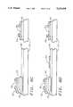
- FIG. 3is a sectional view, in greatly enlarged scale and in broken section, of a single light controlled electrostatic discharge device used in the manufacturing.
- FIG. 4is a sectional view of an alternate embodiment of a discharge device provided with a light blocking element.
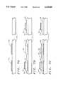
- FIG. 5is a simplified top plan view of an array of scan and data lines which illustrates the elements and their arrangement used in the practice of a first embodiment of the process of the invention.
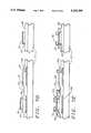
- FIG. 6is a simplified top plan view of any array, similar to FIG. 5, but including a second embodiment of a discharge line structure.
- FIGS. 7a through 7gis a sequence of cross-sectional views, in broken section, which illustrates a first embodiment process of simultaneously making a thin film transistor array and electrostatic discharge protection devices.
- FIGS. 8a through 8fis a sequence of cross-sectional views which illustrates a second embodiment process for simultaneously making a thin film transistor array and electrostatic discharge protection devices.
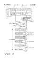
- FIG. 9is a flow diagram which illustrates a first method embodiment of the fabrication, testing and assembling a display panel of the invention.
- FIG. 10is a flow diagram which illustrates a second method embodiment of the fabrication, testing and assembling a display panel of the invention.
- a plurality of spaced parallel conductive scan lines 12are formed on substrate 22, using conventional deposition and patterning techniques.
- Substrate 22can be any suitable type of substrate, typically a glass plate.
- a suitable insulating layerhas been deposited over scan lines 12
- a plurality of spaced, parallel orthogonally arranged conductive data lines 14are deposited.
- Data pads 20 associated with lines 14can be deposited simultaneously.
- An electrostatic discharge line or ring 24is formed that surrounds the data pads 20, and is spaced therefrom.
- a plurality of light controlled electrostatic discharge devices 26,are fabricated which interconnect each of the pads 20 with the electrostatic discharge line 24. Devices 26 function to either electrically isolate data pads 20, or alternately short all the pads 20 and their associated scan and data lines through discharge ring 24. Devices 26 are either non-conducting or conducting, depending on whether they are blocked out or illuminated.
- the conductive data lines 14, a plurality of spaced, lines parallel with each other and orthogonally arranged with scan lines 12,are deposited.
- Scan lines 12can be formed simultaneously with the gate electrode of the transistors, and data lines 14 can be formed simultaneously with the source/drain electrodes of the transistors.
- Contact pads 20can be formed simultaneously with the transparent pixel electrode 33 or the data lines 14.
- the insulating layer of the crossovers of the data lines 14 and scan lines 12is the gate insulating layer of the transistor.
- FIG. 6there is shown a second embodiment of the LCD panel structure and manufacturing process for making such a panel according to the invention.
- This second embodimentis generally similar to the first embodiment except that it provides an alternate structure when the discharge devices cannot be effectively illuminated. This condition may persist during various process steps used to fabricate the array of optical display elements, such as spin drying, etc., when sufficient illumination to the discharge devices 26 can not be provided to assure dependable conduction. If there is insufficient illumination, the data pads 26 would not be shorted to discharge ring 24 in the first embodiment, possibly resulting in damage to the array.
- an additional electrostatic discharge line or ring 42, outside ring 24,is provided. Individual lines 44, isolated from ring 24 join the data pads 20 to ring 42.
- the second embodiment processis similar to the first, i.e. address lines 12, data lines 14, data pads 20, a first elecrostatic line 24, and discharge devices 26 are formed.
- a second electrostatic line 42 and connecting lines 44are formed at the same time.
- the first embodimentrequired that discharge devices 26 be illuminated as the optical display devices were fabricated. However, in this second embodiment, this illumination is not required.
- the second discharge ring 42, and lines 44perform the function of shorting the pads 20.
- the discharge ring 42is removed, and the process proceeds similar to the first embodiment, i.e. the blocking the discharge devices 26, testing the array, removing the blocking and illuminating discharge devices 26 and applying the liquid crystal material.
- the discharge devicesmust again be blocked.
- FIGS. 7athrough 7gshow the process of making these devices.
- the first step of the processcomprises forming, on a glass substrate or other transparent substrate 22, a gate 36 of the transistor, an electrode 18a of the capacitor 18 and the scan lines 12 (not shown), using well known methods of lithography including masking and etching.
- a gate insulating layer 28, amorphous silicon (a-Si:H) layer 30, and a doped amorphous silicon (N+ a-Si:H) layer 32are deposited by plasma enhanced chemical vapor deposition techniques.
- the active regions of the transistor and the photosensitive deviceare formed by lithography. As shown in FIG.
- the transparent pixel electrode 33preferably made of Indium Tin Oxide (ITO) of display element and the pads 20 for data lines 14 and scan lines 12 are formed. Note that the pads 20 for data lines 14 and scan lines 12 could be formed simultaneously with data lines 14.
- layer 34is deposited and the source/drain electrodes of the TFT, contact electrodes of the discharge devices 26, and data lines 14 of the panel are formed by deposition and lithography/etching processing.
- the N+ a-Si:H layersare etched, as seen in FIG. 7f between the source electrode and the drain electrode of the TFT and between the two electrodes of the photosensitive electrostatic discharge device 26.
- the passivation layer 38is deposited over the upper surfaces. This layer may be, for example silicon nitride and deposited by plasma enhanced chemical vapor deposition.
- the shorting ringcan be composed of Metal I and formed when can lines and gates are formed.
- the Metal IIcan be the material of the data lines and source/drain electrodes and may be formed simultaneously.
- the transparent ITOis the material of the pixel electrode.
- the process of forming the thin film transistoris described to indicate where and when the discharge devices and discharge lines, which are key parts of the invention can be fabricated most effectively in the process.
- FIG. 3illustrates separately an embodiment of a discharge device 26A used in the invention.
- the deviceis similar to the device illustrated in the right sides of FIGS. 7a through 7g, which illustrates how it and the TFT may be formed.
- FIG. 4depicts a light controlled device 26B similar to the device 26A, except that a blocking pad 36 is provided beneath layer 30 to shield it from illumination from beneath substrate 22.
- Device 26Bis fabricated in basically the same manner as device 26A, described previously.
- a metal layer 36preferably of chromium is deposited and patterned on substrate 22 to form the gate electrode of the TFT.
- Insulating layer 28is deposited and composed, preferably of silicon nitride.
- An amorphous silicon or polysilicon layer 30is deposited and a silicon nitride layer 35 deposited over layer 30 and patterned to leave areas over the TFT and the discharge device.
- a doped amorphous silicon layer 32is deposited over layer 30 and patterned to form contacts to the end portions of areas of layer 30, as shown in FIG. 8c. Terminals are formed to the source and drain of the TFT and to the ends of the discharge device by the depositions and patterning of the conductive layer 34, which is preferably composed of aluminum/chromium.
- FIG. 9there is depicted a flow chart setting forth the steps in the first embodiment of the invention. Note that the blocks that correspond to the blocks on FIG. 2 have the same numbers. These process steps have been explained previously in regard to FIG. 2.
- the substrateis illuminated during the process steps for forming the active matrix array, as indicated by block 13. Illumination shorts the scan and data lines to the discharge line 24 thereby dispelling any static electricity formed during the process steps.
- the matrix arrayAfter the matrix array is completed it must be electrically tested, since the production yield of the TFT array is normally quite low. If the array is defective, it must be either repaired or discarded, rather than assembled with the second substrate and completed to produce an expensive and useless display panel.
- the pads of the scan lines and data linesmust be electrically isolated from each other. Therefore, the discharge devices 26 must be blocked out, that is prevented from being illuminated.
- the intense lightis illuminated to the first glass substrate to again make the discharge devices conductive, and short the pads through ring 24.
- a thin alignment layersuch as polyimide is coated on each glass, and the surface is rubbed with something, usually a soft cloth, in some direction as the LC molecules will be aligned. In order to form a twisting angle between both glasses, such rubbing directions are different from each other.
- the intense lightis illuminated from the back side of the glass, and the discharge devices are turned on, thus the generated electrostatic charges due to rubbing are discharged through the discharge devices.
- spacing materialsare uniformly scattered on the glass followed by printing of the adhesive material to make the cell.
- the two glassesare now assembled to make a LC cell with proper alignment technique between the two glasses.
- the liquid crystal materialis injected into the cell through the filling opening hole. Usually this process is done in a vacuum chamber.
- the TFT arraymust be electrically tested again.
- the pads of scan lines 12 and data lines 14must be electrically isolated from each other.
- the discharge devicesmust be blocked out again, that is prevented from being illuminated. This can be achieved by putting the LC cell into a dark testing box.
- the LC cellis tested with external components.
- Plastic polarizersare carefully adhered to both sides of the LC cell.
- Driving and peripheral circuit of large scale integrationis connected to the scan pads and the data pads of the LC cell.
- the intense lightis illuminated to the first glass except for the testing processed.
- the static electricityis prevented from doing damage to the array because all the elements are at the same potential.
- steps 21, 23, 25, where the possibility of generating static electricity existsthe substrate is illuminated to again short the scan and data lines through line 24, as indicated in FIG. 9.
- the array in the assembly of substratesis tested in darkness to isolate the scan and data lines.
- FIG. 10depicts the process of the second embodiment of the invention.
- the substrate supporting the TFT array, fabricated with the discharge line 24 and discharge devices 26, and a second discharge line 42 that is directly joined to the pads 20 and illustrated in FIG. 6is used in this process embodiment.
- the process stepsare performed while the substrate is illuminated for the same reasons described for the first embodiment.
- the scan and data linesare shorted by line 42 so that there is no requirement that the discharge devices be illuminated. This shorting arrangement may be necessary where the discharge devices can not conveniently be illuminated to activate the discharge devices.
- the shorting line 42must be removed, as by cutting the glass substrate before the array is tested, as indicated by block 42.
- the test of the fabrication processis similar to the process of the first embodiment, describe previously.
Landscapes
- Physics & Mathematics (AREA)
- Nonlinear Science (AREA)
- Engineering & Computer Science (AREA)
- Microelectronics & Electronic Packaging (AREA)
- Mathematical Physics (AREA)
- Chemical & Material Sciences (AREA)
- Crystallography & Structural Chemistry (AREA)
- General Physics & Mathematics (AREA)
- Optics & Photonics (AREA)
- Liquid Crystal (AREA)
Abstract
Description
Claims (32)
Priority Applications (1)
| Application Number | Priority Date | Filing Date | Title |
|---|---|---|---|
| US07/877,711US5233448A (en) | 1992-05-04 | 1992-05-04 | Method of manufacturing a liquid crystal display panel including photoconductive electrostatic protection |
Applications Claiming Priority (1)
| Application Number | Priority Date | Filing Date | Title |
|---|---|---|---|
| US07/877,711US5233448A (en) | 1992-05-04 | 1992-05-04 | Method of manufacturing a liquid crystal display panel including photoconductive electrostatic protection |
Publications (1)
| Publication Number | Publication Date |
|---|---|
| US5233448Atrue US5233448A (en) | 1993-08-03 |
Family
ID=25370561
Family Applications (1)
| Application Number | Title | Priority Date | Filing Date |
|---|---|---|---|
| US07/877,711Expired - LifetimeUS5233448A (en) | 1992-05-04 | 1992-05-04 | Method of manufacturing a liquid crystal display panel including photoconductive electrostatic protection |
Country Status (1)
| Country | Link |
|---|---|
| US (1) | US5233448A (en) |
Cited By (76)
| Publication number | Priority date | Publication date | Assignee | Title |
|---|---|---|---|---|
| US5497146A (en)* | 1992-06-03 | 1996-03-05 | Frontec, Incorporated | Matrix wiring substrates |
| US5504348A (en)* | 1992-08-13 | 1996-04-02 | Casio Computer Co., Ltd. | Thin-film transistor array and liquid crystal display device using the thin-film transistor array |
| WO1996007300A3 (en)* | 1994-08-20 | 1996-05-02 | Philips Electronics Nv | Manufacture of electronic devices comprising thin-film circuitry |
| US5517342A (en)* | 1993-03-04 | 1996-05-14 | Samsung Electronics Co., Ltd. | Liquid crystal display having additional capacitors formed from pixel electrodes and a method for manufacturing the same |
| US5546204A (en)* | 1994-05-26 | 1996-08-13 | Honeywell Inc. | TFT matrix liquid crystal device having data source lines and drain means of etched and doped single crystal silicon |
| US5561381A (en)* | 1989-12-13 | 1996-10-01 | International Business Machines Corporation | Method for testing a partially constructed electronic circuit |
| US5576730A (en)* | 1992-04-08 | 1996-11-19 | Sharp Kabushiki Kaisha | Active matrix substrate and a method for producing the same |
| GB2307087A (en)* | 1995-08-19 | 1997-05-14 | Lg Electronics Inc | Liquid crystal displays |
| US5650834A (en)* | 1994-07-05 | 1997-07-22 | Mitsubishi Denki Kabushiki Kaisha | Active-matrix device having silicide thin film resistor disposed between an input terminal and a short-circuit ring |
| US5652632A (en)* | 1994-09-30 | 1997-07-29 | Nec Corporation | LCD apparatus having electrostatic breakdown preventing configuration capable of testing each pixel |
| US5657139A (en)* | 1994-09-30 | 1997-08-12 | Kabushiki Kaisha Toshiba | Array substrate for a flat-display device including surge protection circuits and short circuit line or lines |
| US5671026A (en)* | 1994-03-02 | 1997-09-23 | Sharp Kabushiki Kaisha | Liquid crystal display device with TFT ESD protective devices between I/O terminals or with a short circuited alignment film |
| US5677745A (en)* | 1994-12-21 | 1997-10-14 | Kabushiki Kaisha Toshiba | LCD with electrostatic discharge projections |
| US5684546A (en)* | 1994-10-06 | 1997-11-04 | Samsung Electronics Co., Ltd. | Electrostatic discharge protective circuit in a liquid crystal display |
| US5689352A (en)* | 1994-06-21 | 1997-11-18 | Casio Computer Co., Ltd. | Liquid crystal display device and process for producing same |
| US5699134A (en)* | 1993-11-17 | 1997-12-16 | Matsushita Electric Industrial Co. Ltd. | Liquid crystal display panel and method for manufacturing the panel |
| US5714770A (en)* | 1995-12-05 | 1998-02-03 | Samsung Electronics Co., Ltd. | Thin film transistor substrate for a liquid crystal display |
| US5767929A (en)* | 1995-09-21 | 1998-06-16 | Advanced Display Inc. | Liquid crystal display apparatus with shorting ring |
| US5841490A (en)* | 1994-10-31 | 1998-11-24 | Kyocera Corporation | Liquid crystal display device and its fabricating method |
| US5875086A (en)* | 1993-06-30 | 1999-02-23 | Nec Corporation | Semiconductor integrated circuit device equipped with protective system for directly discharging surge voltage from pad to discharge line |
| US5949502A (en)* | 1995-08-07 | 1999-09-07 | Hitachi, Ltd. | Liquid crystal device having resistor elements |
| US6005647A (en)* | 1996-07-22 | 1999-12-21 | Lg Electronics Inc. | Shorting bars for a liquid crystal display and method of forming the same |
| US6025891A (en)* | 1996-11-29 | 2000-02-15 | Lg Electronics Inc. | Liquid crystal display device |
| US6043971A (en)* | 1998-11-04 | 2000-03-28 | L.G. Philips Lcd Co., Ltd. | Electrostatic discharge protection device for liquid crystal display using a COG package |
| US6128051A (en)* | 1997-09-12 | 2000-10-03 | Lg Electronics Inc. | Method for forming and apparatus including a liquid crystal display having shorting bar connector |
| US6175394B1 (en)* | 1996-12-03 | 2001-01-16 | Chung-Cheng Wu | Capacitively coupled field effect transistors for electrostatic discharge protection in flat panel displays |
| US6239850B1 (en)* | 1996-05-08 | 2001-05-29 | Semiconductor Energy Laboratory Co., Ltd. | Liquid crystal electro-optical device and process of fabricating same provided with discharge accelerating patterns for minimizing dielectric breakdown |
| US6411351B1 (en) | 1996-02-13 | 2002-06-25 | Semiconductor Energy Laboratory Co., Ltd. | Active matrix type display device comprising a discharge pattern or a short ring and method of manufacturing the same |
| US6411348B2 (en)* | 1996-07-02 | 2002-06-25 | Sharp Kabushiki Kaisha | Active matrix substrate and producing method of the same |
| US6493047B2 (en)* | 1997-08-07 | 2002-12-10 | Lg. Philips Lcd Co., Ltd. | Liquid crystal display panel having electrostatic discharge prevention circuitry |
| US6587160B2 (en)* | 1997-10-14 | 2003-07-01 | Samsung Electronics Co., Ltd. | Liquid crystal displays |
| US20040032278A1 (en)* | 2001-08-03 | 2004-02-19 | Toshihiko Orii | Inspecting method, semiconductor device, and display |
| US6697037B1 (en) | 1996-04-29 | 2004-02-24 | International Business Machines Corporation | TFT LCD active data line repair |
| US20040222813A1 (en)* | 2003-05-06 | 2004-11-11 | Kim Jong Dam | Method and apparatus for testing liquid crystal display |
| US20050046774A1 (en)* | 2002-04-20 | 2005-03-03 | Choi Seung Kyu | Liquid crystal display |
| US20050052393A1 (en)* | 2003-08-26 | 2005-03-10 | Seiko Epson Corporation | Method of driving liquid crystal display device, liquid crystal display device, and portable electronic apparatus |
| US20050180072A1 (en)* | 2004-02-16 | 2005-08-18 | Han-Chung Lai | Electrostatic discharge guide and liquid crystal display utilizing same |
| US20060092591A1 (en)* | 2004-10-28 | 2006-05-04 | Quan Yuan | On-substrate ESD protection for array based image sensors |
| US20060186097A1 (en)* | 2004-05-05 | 2006-08-24 | Micron Technology, Inc. | Systems and methods for forming apertures in microfeature workpieces |
| US20060240687A1 (en)* | 2004-08-27 | 2006-10-26 | Micron Technology, Inc. | Slanted vias for electrical circuits on circuit boards and other substrates |
| US20070007526A1 (en)* | 2005-07-08 | 2007-01-11 | Saori Sugiyama | Display panel and display device |
| US20070045826A1 (en)* | 2005-09-01 | 2007-03-01 | Micron Technology, Inc. | Microfeature workpiece substrates having through-substrate vias, and associated methods of formation |
| US20070046845A1 (en)* | 2005-08-30 | 2007-03-01 | Chunghwa Picture Tubes., Ltd | Liquid crystal display panel with electrostatic discharge protection |
| US20070045120A1 (en)* | 2005-09-01 | 2007-03-01 | Micron Technology, Inc. | Methods and apparatus for filling features in microfeature workpieces |
| US20070049016A1 (en)* | 2005-09-01 | 2007-03-01 | Micron Technology, Inc. | Microfeature workpieces and methods for forming interconnects in microfeature workpieces |
| CN1319168C (en)* | 2003-11-04 | 2007-05-30 | 友达光电股份有限公司 | Electrostatic discharge protection mechanism and liquid crystal display panel using the mechanism |
| US20070267754A1 (en)* | 2005-09-01 | 2007-11-22 | Micron Technology, Inc. | Microfeature workpieces and methods for forming interconnects in microfeature workpieces |
| US20070281473A1 (en)* | 2006-06-01 | 2007-12-06 | Micron Technology, Inc. | Microelectronic workpieces and methods and systems for forming interconnects in microelectronic workpieces |
| US20080054444A1 (en)* | 2006-08-31 | 2008-03-06 | Micron Technology, Inc. | Microfeature workpieces having interconnects and conductive backplanes, and associated systems and methods |
| US20080111213A1 (en)* | 2004-09-02 | 2008-05-15 | Micron Technology, Inc. | Through-wafer interconnects for photoimager and memory wafers |
| CN100389341C (en)* | 2005-08-08 | 2008-05-21 | 友达光电股份有限公司 | Active element array substrate |
| US7413979B2 (en) | 2003-11-13 | 2008-08-19 | Micron Technology, Inc. | Methods for forming vias in microelectronic devices, and methods for packaging microelectronic devices |
| US7425499B2 (en) | 2004-08-24 | 2008-09-16 | Micron Technology, Inc. | Methods for forming interconnects in vias and microelectronic workpieces including such interconnects |
| US20090008780A1 (en)* | 2004-12-30 | 2009-01-08 | Micron Technology, Inc. | Methods for forming interconnects in microelectronic workpieces and microelectronic workpieces formed using such methods |
| US20090057912A1 (en)* | 2007-08-31 | 2009-03-05 | Micron Technology, Inc. | Partitioned through-layer via and associated systems and methods |
| US7531453B2 (en) | 2004-06-29 | 2009-05-12 | Micron Technology, Inc. | Microelectronic devices and methods for forming interconnects in microelectronic devices |
| US20090146312A1 (en)* | 2007-12-06 | 2009-06-11 | Micron Technology, Inc. | Methods for forming interconnects in microelectronic workpieces and microelectronic workpieces formed using such methods |
| US20090166846A1 (en)* | 2007-12-28 | 2009-07-02 | Micron Technology, Inc. | Pass-through 3d interconnect for microelectronic dies and associated systems and methods |
| US20090242888A1 (en)* | 2008-03-31 | 2009-10-01 | Semiconductor Energy Laboratory Co., Ltd. | Display Device and Method for Manufacturing the Same |
| US20090256981A1 (en)* | 2008-04-11 | 2009-10-15 | Innolux Display Corp. | Liquid crystal display having protection element |
| US20090283898A1 (en)* | 2008-05-15 | 2009-11-19 | Janzen Jeffery W | Disabling electrical connections using pass-through 3d interconnects and associated systems and methods |
| US7629249B2 (en) | 2006-08-28 | 2009-12-08 | Micron Technology, Inc. | Microfeature workpieces having conductive interconnect structures formed by chemically reactive processes, and associated systems and methods |
| US20100084653A1 (en)* | 2008-10-03 | 2010-04-08 | Semiconductor Energy Laboratory Co., Ltd. | Display device |
| US7795134B2 (en) | 2005-06-28 | 2010-09-14 | Micron Technology, Inc. | Conductive interconnect structures and formation methods using supercritical fluids |
| USRE41669E1 (en) | 2002-05-10 | 2010-09-14 | Ponnusamy Palanisamy | Low-cost circuit board materials and processes for area array electrical interconnections over a large area between a device and the circuit board |
| USRE41914E1 (en) | 2002-05-10 | 2010-11-09 | Ponnusamy Palanisamy | Thermal management in electronic displays |
| CN102097059A (en)* | 2009-12-10 | 2011-06-15 | 精工爱普生株式会社 | Protection circuit, substrate for electro-optical device, electrophoretic display device, electronic apparatus, electro-optical device, and manufacturing method of electro-optical device |
| CN101089685B (en)* | 2006-06-15 | 2011-08-10 | 乐金显示有限公司 | Array substrate for liquid crystal display device |
| US8084866B2 (en) | 2003-12-10 | 2011-12-27 | Micron Technology, Inc. | Microelectronic devices and methods for filling vias in microelectronic devices |
| US8368066B2 (en) | 2008-10-03 | 2013-02-05 | Semiconductor Energy Laboratory Co., Ltd. | Display device |
| US20130069682A1 (en)* | 2011-09-20 | 2013-03-21 | United Microelectronics Corporation | Circuit structure of test-key and test method thereof |
| US20130321728A1 (en)* | 2012-05-30 | 2013-12-05 | Shenzhen China Star Optoelectronics Technology Co, Ltd. | Susbtrate for Array Process of Panel Display Device, Manufacturing Method and Corresponding Liquid Crystal Display Device |
| US20140375344A1 (en)* | 2013-06-20 | 2014-12-25 | Shenzhen China Star Optoelectronics Technology Co., Ltd. | Liquid crystal panel, and testing circuit and testing method thereof |
| US20150084038A1 (en)* | 2011-10-21 | 2015-03-26 | Silicon Display Technology | Intensified sensor array for static electricity |
| CN106226964A (en)* | 2016-07-27 | 2016-12-14 | 武汉华星光电技术有限公司 | There is array base palte and the display floater thereof of antistatic protection function |
| US11362081B2 (en)* | 2004-07-05 | 2022-06-14 | 138 East Lcd Advancements Limited | Semiconductor device, display device, and electronic apparatus |
Citations (6)
| Publication number | Priority date | Publication date | Assignee | Title |
|---|---|---|---|---|
| EP0236167A1 (en)* | 1986-01-27 | 1987-09-09 | François Maurice | Display screen provided with an active matrix with redundant lines and columns |
| JPS64931A (en)* | 1987-06-24 | 1989-01-05 | Ricoh Co Ltd | Liquid crystal display panel |
| JPH02210420A (en)* | 1989-02-10 | 1990-08-21 | Hitachi Ltd | Production of liquid crystal panel |
| JPH032838A (en)* | 1989-05-31 | 1991-01-09 | Matsushita Electron Corp | Production of liquid crystal display device |
| US5068748A (en)* | 1989-10-20 | 1991-11-26 | Hosiden Corporation | Active matrix liquid crystal display device having improved electrostatic discharge protection |
| US5200876A (en)* | 1989-04-10 | 1993-04-06 | Matsushita Electric Industrial Co., Ltd. | Electrostatic breakdown protection circuit |
- 1992
- 1992-05-04USUS07/877,711patent/US5233448A/ennot_activeExpired - Lifetime
Patent Citations (6)
| Publication number | Priority date | Publication date | Assignee | Title |
|---|---|---|---|---|
| EP0236167A1 (en)* | 1986-01-27 | 1987-09-09 | François Maurice | Display screen provided with an active matrix with redundant lines and columns |
| JPS64931A (en)* | 1987-06-24 | 1989-01-05 | Ricoh Co Ltd | Liquid crystal display panel |
| JPH02210420A (en)* | 1989-02-10 | 1990-08-21 | Hitachi Ltd | Production of liquid crystal panel |
| US5200876A (en)* | 1989-04-10 | 1993-04-06 | Matsushita Electric Industrial Co., Ltd. | Electrostatic breakdown protection circuit |
| JPH032838A (en)* | 1989-05-31 | 1991-01-09 | Matsushita Electron Corp | Production of liquid crystal display device |
| US5068748A (en)* | 1989-10-20 | 1991-11-26 | Hosiden Corporation | Active matrix liquid crystal display device having improved electrostatic discharge protection |
Cited By (173)
| Publication number | Priority date | Publication date | Assignee | Title |
|---|---|---|---|---|
| US5561381A (en)* | 1989-12-13 | 1996-10-01 | International Business Machines Corporation | Method for testing a partially constructed electronic circuit |
| US5576730A (en)* | 1992-04-08 | 1996-11-19 | Sharp Kabushiki Kaisha | Active matrix substrate and a method for producing the same |
| US5497146A (en)* | 1992-06-03 | 1996-03-05 | Frontec, Incorporated | Matrix wiring substrates |
| US5504348A (en)* | 1992-08-13 | 1996-04-02 | Casio Computer Co., Ltd. | Thin-film transistor array and liquid crystal display device using the thin-film transistor array |
| US5517342A (en)* | 1993-03-04 | 1996-05-14 | Samsung Electronics Co., Ltd. | Liquid crystal display having additional capacitors formed from pixel electrodes and a method for manufacturing the same |
| US5995175A (en)* | 1993-03-04 | 1999-11-30 | Samsung Electronics Co., Ltd. | Liquid crystal display and a method for manufacturing the same |
| US5875086A (en)* | 1993-06-30 | 1999-02-23 | Nec Corporation | Semiconductor integrated circuit device equipped with protective system for directly discharging surge voltage from pad to discharge line |
| US5699134A (en)* | 1993-11-17 | 1997-12-16 | Matsushita Electric Industrial Co. Ltd. | Liquid crystal display panel and method for manufacturing the panel |
| US5671026A (en)* | 1994-03-02 | 1997-09-23 | Sharp Kabushiki Kaisha | Liquid crystal display device with TFT ESD protective devices between I/O terminals or with a short circuited alignment film |
| US5926234A (en)* | 1994-03-02 | 1999-07-20 | Sharp Kabushiki Kaisha | Liquid crystal display device |
| US5546204A (en)* | 1994-05-26 | 1996-08-13 | Honeywell Inc. | TFT matrix liquid crystal device having data source lines and drain means of etched and doped single crystal silicon |
| US5689352A (en)* | 1994-06-21 | 1997-11-18 | Casio Computer Co., Ltd. | Liquid crystal display device and process for producing same |
| US5650834A (en)* | 1994-07-05 | 1997-07-22 | Mitsubishi Denki Kabushiki Kaisha | Active-matrix device having silicide thin film resistor disposed between an input terminal and a short-circuit ring |
| WO1996007300A3 (en)* | 1994-08-20 | 1996-05-02 | Philips Electronics Nv | Manufacture of electronic devices comprising thin-film circuitry |
| US5652632A (en)* | 1994-09-30 | 1997-07-29 | Nec Corporation | LCD apparatus having electrostatic breakdown preventing configuration capable of testing each pixel |
| US5657139A (en)* | 1994-09-30 | 1997-08-12 | Kabushiki Kaisha Toshiba | Array substrate for a flat-display device including surge protection circuits and short circuit line or lines |
| US5684546A (en)* | 1994-10-06 | 1997-11-04 | Samsung Electronics Co., Ltd. | Electrostatic discharge protective circuit in a liquid crystal display |
| US5841490A (en)* | 1994-10-31 | 1998-11-24 | Kyocera Corporation | Liquid crystal display device and its fabricating method |
| US5677745A (en)* | 1994-12-21 | 1997-10-14 | Kabushiki Kaisha Toshiba | LCD with electrostatic discharge projections |
| US5949502A (en)* | 1995-08-07 | 1999-09-07 | Hitachi, Ltd. | Liquid crystal device having resistor elements |
| US5825449A (en)* | 1995-08-19 | 1998-10-20 | Lg Electronics, Inc. | Liquid crystal display device and method of manufacturing the same |
| US5828433A (en)* | 1995-08-19 | 1998-10-27 | Lg Electronics Inc. | Liquid crystal display device and a method of manufacturing the same |
| GB2307087B (en)* | 1995-08-19 | 2000-03-22 | Lg Electronics Inc | Liquid crystal display device and a method of manufacturing the same |
| GB2307087A (en)* | 1995-08-19 | 1997-05-14 | Lg Electronics Inc | Liquid crystal displays |
| US5767929A (en)* | 1995-09-21 | 1998-06-16 | Advanced Display Inc. | Liquid crystal display apparatus with shorting ring |
| US5714770A (en)* | 1995-12-05 | 1998-02-03 | Samsung Electronics Co., Ltd. | Thin film transistor substrate for a liquid crystal display |
| US6646693B2 (en)* | 1996-02-13 | 2003-11-11 | Semiconductor Energy Laboratory Co., Ltd. | Manufacturing method for an active matrix display including a capacitor formed from a short ring electrode |
| US7425999B2 (en) | 1996-02-13 | 2008-09-16 | Semiconductor Energy Laboratory Co., Ltd. | Electro-optical device and manufacturing method thereof |
| US20040165831A1 (en)* | 1996-02-13 | 2004-08-26 | Semiconductor Energy Laboratory Co., Ltd. A Japan Corporation | Electro-optical device and manufacturing method thereof |
| US20060189025A1 (en)* | 1996-02-13 | 2006-08-24 | Semiconductor Energy Laboratory Co., Ltd. | Electro-optical device and manufacturing method thereoff |
| US7057677B2 (en)* | 1996-02-13 | 2006-06-06 | Semiconductor Energy Laboratory Co., Ltd. | Electro-optical device and manufacturing method thereof |
| US6411351B1 (en) | 1996-02-13 | 2002-06-25 | Semiconductor Energy Laboratory Co., Ltd. | Active matrix type display device comprising a discharge pattern or a short ring and method of manufacturing the same |
| US6697037B1 (en) | 1996-04-29 | 2004-02-24 | International Business Machines Corporation | TFT LCD active data line repair |
| US6239850B1 (en)* | 1996-05-08 | 2001-05-29 | Semiconductor Energy Laboratory Co., Ltd. | Liquid crystal electro-optical device and process of fabricating same provided with discharge accelerating patterns for minimizing dielectric breakdown |
| US6411348B2 (en)* | 1996-07-02 | 2002-06-25 | Sharp Kabushiki Kaisha | Active matrix substrate and producing method of the same |
| US6005647A (en)* | 1996-07-22 | 1999-12-21 | Lg Electronics Inc. | Shorting bars for a liquid crystal display and method of forming the same |
| US6100949A (en)* | 1996-11-29 | 2000-08-08 | Lg Electronics Inc. | Liquid crystal display device having electrostatic discharge protection |
| US6025891A (en)* | 1996-11-29 | 2000-02-15 | Lg Electronics Inc. | Liquid crystal display device |
| US6175394B1 (en)* | 1996-12-03 | 2001-01-16 | Chung-Cheng Wu | Capacitively coupled field effect transistors for electrostatic discharge protection in flat panel displays |
| US6493047B2 (en)* | 1997-08-07 | 2002-12-10 | Lg. Philips Lcd Co., Ltd. | Liquid crystal display panel having electrostatic discharge prevention circuitry |
| US6128051A (en)* | 1997-09-12 | 2000-10-03 | Lg Electronics Inc. | Method for forming and apparatus including a liquid crystal display having shorting bar connector |
| US20070064165A1 (en)* | 1997-10-14 | 2007-03-22 | Lee Joo-Hyung | Thin film transistor array panel |
| US6587160B2 (en)* | 1997-10-14 | 2003-07-01 | Samsung Electronics Co., Ltd. | Liquid crystal displays |
| US7986379B2 (en) | 1997-10-14 | 2011-07-26 | Samsung Electronics Co., Ltd. | Thin film transistor array panel |
| US7710506B2 (en) | 1997-10-14 | 2010-05-04 | Samsung Electronics Co., Ltd. | Thin film transistor array panel |
| US7139044B2 (en) | 1997-10-14 | 2006-11-21 | Samsung Electronics Co., Ltd. | Thin film transistor array panel |
| US20100181572A1 (en)* | 1997-10-14 | 2010-07-22 | Lee Joo-Hyung | Thin film transistor array panel |
| US6043971A (en)* | 1998-11-04 | 2000-03-28 | L.G. Philips Lcd Co., Ltd. | Electrostatic discharge protection device for liquid crystal display using a COG package |
| US20050200377A1 (en)* | 2001-08-03 | 2005-09-15 | Sony Corporation | Testing method, semiconductor device, and display apparatus |
| US20040032278A1 (en)* | 2001-08-03 | 2004-02-19 | Toshihiko Orii | Inspecting method, semiconductor device, and display |
| US7009418B2 (en)* | 2001-08-03 | 2006-03-07 | Sony Corporation | Inspecting method, semiconductor device, and display apparatus |
| US7123044B2 (en)* | 2001-08-03 | 2006-10-17 | Sony Corporation | Testing method, semiconductor device, and display apparatus |
| US7176990B2 (en)* | 2002-04-20 | 2007-02-13 | Lg.Phillips Lcd Co., Ltd | Liquid crystal display |
| US20050046774A1 (en)* | 2002-04-20 | 2005-03-03 | Choi Seung Kyu | Liquid crystal display |
| USRE41669E1 (en) | 2002-05-10 | 2010-09-14 | Ponnusamy Palanisamy | Low-cost circuit board materials and processes for area array electrical interconnections over a large area between a device and the circuit board |
| USRE42542E1 (en) | 2002-05-10 | 2011-07-12 | Transpacific Infinity, Llc | Low-cost circuit board materials and processes for area array electrical interconnections over a large area between a device and the circuit board |
| USRE41914E1 (en) | 2002-05-10 | 2010-11-09 | Ponnusamy Palanisamy | Thermal management in electronic displays |
| US7132846B2 (en)* | 2003-05-06 | 2006-11-07 | Lg.Phillips Lcd Co., Ltd. | Method and apparatus for testing liquid crystal display |
| US20070024315A1 (en)* | 2003-05-06 | 2007-02-01 | Kim Jong D | Method and apparatus for testing liquid crystal display |
| US20040222813A1 (en)* | 2003-05-06 | 2004-11-11 | Kim Jong Dam | Method and apparatus for testing liquid crystal display |
| US7362124B2 (en) | 2003-05-06 | 2008-04-22 | Lg.Philips Lcd Co., Ltd. | Method and apparatus for testing liquid crystal display using electrostatic devices |
| US20050052393A1 (en)* | 2003-08-26 | 2005-03-10 | Seiko Epson Corporation | Method of driving liquid crystal display device, liquid crystal display device, and portable electronic apparatus |
| US7414602B2 (en)* | 2003-08-26 | 2008-08-19 | Seiko Epson Corporation | Method of driving liquid crystal display device, liquid crystal display device, and portable electronic apparatus |
| US8248338B2 (en) | 2003-08-26 | 2012-08-21 | Seiko Epson Corporation | Method of driving liquid crystal display device, liquid crystal display device, and portable electronic apparatus |
| CN1319168C (en)* | 2003-11-04 | 2007-05-30 | 友达光电股份有限公司 | Electrostatic discharge protection mechanism and liquid crystal display panel using the mechanism |
| US7759800B2 (en) | 2003-11-13 | 2010-07-20 | Micron Technology, Inc. | Microelectronics devices, having vias, and packaged microelectronic devices having vias |
| US7413979B2 (en) | 2003-11-13 | 2008-08-19 | Micron Technology, Inc. | Methods for forming vias in microelectronic devices, and methods for packaging microelectronic devices |
| US9653420B2 (en) | 2003-11-13 | 2017-05-16 | Micron Technology, Inc. | Microelectronic devices and methods for filling vias in microelectronic devices |
| US11177175B2 (en) | 2003-12-10 | 2021-11-16 | Micron Technology, Inc. | Microelectronic devices and methods for filling vias in microelectronic devices |
| US8084866B2 (en) | 2003-12-10 | 2011-12-27 | Micron Technology, Inc. | Microelectronic devices and methods for filling vias in microelectronic devices |
| US8748311B2 (en) | 2003-12-10 | 2014-06-10 | Micron Technology, Inc. | Microelectronic devices and methods for filing vias in microelectronic devices |
| US20080024947A1 (en)* | 2004-02-16 | 2008-01-31 | Au Optronics Corp. | Electrostatic discharge guide and liquid crystal display utilizing same |
| US7317602B2 (en)* | 2004-02-16 | 2008-01-08 | Au Optronics Corp. | Electrostatic discharge guide and liquid crystal display utilizing same |
| US20050180072A1 (en)* | 2004-02-16 | 2005-08-18 | Han-Chung Lai | Electrostatic discharge guide and liquid crystal display utilizing same |
| US7474516B2 (en) | 2004-02-16 | 2009-01-06 | Au Optronics Corp. | Electrostatic discharge guide and liquid crystal display utilizing same |
| US20060186097A1 (en)* | 2004-05-05 | 2006-08-24 | Micron Technology, Inc. | Systems and methods for forming apertures in microfeature workpieces |
| US8686313B2 (en) | 2004-05-05 | 2014-04-01 | Micron Technology, Inc. | System and methods for forming apertures in microfeature workpieces |
| US9452492B2 (en) | 2004-05-05 | 2016-09-27 | Micron Technology, Inc. | Systems and methods for forming apertures in microfeature workpieces |
| US8664562B2 (en) | 2004-05-05 | 2014-03-04 | Micron Technology, Inc. | Systems and methods for forming apertures in microfeature workpieces |
| US10010977B2 (en) | 2004-05-05 | 2018-07-03 | Micron Technology, Inc. | Systems and methods for forming apertures in microfeature workpieces |
| US8536485B2 (en) | 2004-05-05 | 2013-09-17 | Micron Technology, Inc. | Systems and methods for forming apertures in microfeature workpieces |
| US20060191882A1 (en)* | 2004-05-05 | 2006-08-31 | Micron Technology, Inc. | Systems and methods for forming apertures in microfeature workpieces |
| US7829976B2 (en) | 2004-06-29 | 2010-11-09 | Micron Technology, Inc. | Microelectronic devices and methods for forming interconnects in microelectronic devices |
| US7531453B2 (en) | 2004-06-29 | 2009-05-12 | Micron Technology, Inc. | Microelectronic devices and methods for forming interconnects in microelectronic devices |
| US11362081B2 (en)* | 2004-07-05 | 2022-06-14 | 138 East Lcd Advancements Limited | Semiconductor device, display device, and electronic apparatus |
| US7425499B2 (en) | 2004-08-24 | 2008-09-16 | Micron Technology, Inc. | Methods for forming interconnects in vias and microelectronic workpieces including such interconnects |
| US7435913B2 (en) | 2004-08-27 | 2008-10-14 | Micron Technology, Inc. | Slanted vias for electrical circuits on circuit boards and other substrates |
| US20060240687A1 (en)* | 2004-08-27 | 2006-10-26 | Micron Technology, Inc. | Slanted vias for electrical circuits on circuit boards and other substrates |
| US8322031B2 (en) | 2004-08-27 | 2012-12-04 | Micron Technology, Inc. | Method of manufacturing an interposer |
| US20080111213A1 (en)* | 2004-09-02 | 2008-05-15 | Micron Technology, Inc. | Through-wafer interconnects for photoimager and memory wafers |
| US7956443B2 (en) | 2004-09-02 | 2011-06-07 | Micron Technology, Inc. | Through-wafer interconnects for photoimager and memory wafers |
| US7683458B2 (en) | 2004-09-02 | 2010-03-23 | Micron Technology, Inc. | Through-wafer interconnects for photoimager and memory wafers |
| US20110233777A1 (en)* | 2004-09-02 | 2011-09-29 | Micron Technology, Inc. | Through-wafer interconnects for photoimager and memory wafers |
| US8502353B2 (en) | 2004-09-02 | 2013-08-06 | Micron Technology, Inc. | Through-wafer interconnects for photoimager and memory wafers |
| US8669179B2 (en) | 2004-09-02 | 2014-03-11 | Micron Technology, Inc. | Through-wafer interconnects for photoimager and memory wafers |
| US20100171217A1 (en)* | 2004-09-02 | 2010-07-08 | Micron Technology, Inc. | Through-wafer interconnects for photoimager and memory wafers |
| US20060092591A1 (en)* | 2004-10-28 | 2006-05-04 | Quan Yuan | On-substrate ESD protection for array based image sensors |
| US7532264B2 (en) | 2004-10-28 | 2009-05-12 | Dpix Llc | On-substrate ESD protection for array based image sensors |
| US7589008B2 (en) | 2004-12-30 | 2009-09-15 | Micron Technology, Inc. | Methods for forming interconnects in microelectronic workpieces and microelectronic workpieces formed using such methods |
| US20090008780A1 (en)* | 2004-12-30 | 2009-01-08 | Micron Technology, Inc. | Methods for forming interconnects in microelectronic workpieces and microelectronic workpieces formed using such methods |
| US9214391B2 (en) | 2004-12-30 | 2015-12-15 | Micron Technology, Inc. | Methods for forming interconnects in microelectronic workpieces and microelectronic workpieces formed using such methods |
| US7795134B2 (en) | 2005-06-28 | 2010-09-14 | Micron Technology, Inc. | Conductive interconnect structures and formation methods using supercritical fluids |
| US9293367B2 (en) | 2005-06-28 | 2016-03-22 | Micron Technology, Inc. | Conductive interconnect structures and formation methods using supercritical fluids |
| US8008192B2 (en) | 2005-06-28 | 2011-08-30 | Micron Technology, Inc. | Conductive interconnect structures and formation methods using supercritical fluids |
| US20070007526A1 (en)* | 2005-07-08 | 2007-01-11 | Saori Sugiyama | Display panel and display device |
| US7719650B2 (en)* | 2005-07-08 | 2010-05-18 | Hitachi Displays, Ltd. | Display panel and display device |
| CN100389341C (en)* | 2005-08-08 | 2008-05-21 | 友达光电股份有限公司 | Active element array substrate |
| US7477333B2 (en)* | 2005-08-30 | 2009-01-13 | Chunghwa Picture Tubes, Ltd. | Liquid crystal display panel with electrostatic discharge protection |
| US20070046845A1 (en)* | 2005-08-30 | 2007-03-01 | Chunghwa Picture Tubes., Ltd | Liquid crystal display panel with electrostatic discharge protection |
| US20070045826A1 (en)* | 2005-09-01 | 2007-03-01 | Micron Technology, Inc. | Microfeature workpiece substrates having through-substrate vias, and associated methods of formation |
| US20110079900A1 (en)* | 2005-09-01 | 2011-04-07 | Micron Technology, Inc. | Microfeature workpieces and methods for forming interconnects in microfeature workpieces |
| US7915736B2 (en) | 2005-09-01 | 2011-03-29 | Micron Technology, Inc. | Microfeature workpieces and methods for forming interconnects in microfeature workpieces |
| US20070045120A1 (en)* | 2005-09-01 | 2007-03-01 | Micron Technology, Inc. | Methods and apparatus for filling features in microfeature workpieces |
| US20070049016A1 (en)* | 2005-09-01 | 2007-03-01 | Micron Technology, Inc. | Microfeature workpieces and methods for forming interconnects in microfeature workpieces |
| US7622377B2 (en) | 2005-09-01 | 2009-11-24 | Micron Technology, Inc. | Microfeature workpiece substrates having through-substrate vias, and associated methods of formation |
| US7863187B2 (en) | 2005-09-01 | 2011-01-04 | Micron Technology, Inc. | Microfeature workpieces and methods for forming interconnects in microfeature workpieces |
| US20070267754A1 (en)* | 2005-09-01 | 2007-11-22 | Micron Technology, Inc. | Microfeature workpieces and methods for forming interconnects in microfeature workpieces |
| US12014958B2 (en) | 2005-09-01 | 2024-06-18 | Micron Technology, Inc. | Microfeature workpieces and methods for forming interconnects in microfeature workpieces |
| US11476160B2 (en) | 2005-09-01 | 2022-10-18 | Micron Technology, Inc. | Microfeature workpieces and methods for forming interconnects in microfeature workpieces |
| US20070281473A1 (en)* | 2006-06-01 | 2007-12-06 | Micron Technology, Inc. | Microelectronic workpieces and methods and systems for forming interconnects in microelectronic workpieces |
| US7749899B2 (en) | 2006-06-01 | 2010-07-06 | Micron Technology, Inc. | Microelectronic workpieces and methods and systems for forming interconnects in microelectronic workpieces |
| CN101089685B (en)* | 2006-06-15 | 2011-08-10 | 乐金显示有限公司 | Array substrate for liquid crystal display device |
| US7973411B2 (en) | 2006-08-28 | 2011-07-05 | Micron Technology, Inc. | Microfeature workpieces having conductive interconnect structures formed by chemically reactive processes, and associated systems and methods |
| US8610279B2 (en) | 2006-08-28 | 2013-12-17 | Micron Technologies, Inc. | Microfeature workpieces having conductive interconnect structures formed by chemically reactive processes, and associated systems and methods |
| US7629249B2 (en) | 2006-08-28 | 2009-12-08 | Micron Technology, Inc. | Microfeature workpieces having conductive interconnect structures formed by chemically reactive processes, and associated systems and methods |
| US7902643B2 (en) | 2006-08-31 | 2011-03-08 | Micron Technology, Inc. | Microfeature workpieces having interconnects and conductive backplanes, and associated systems and methods |
| US20080054444A1 (en)* | 2006-08-31 | 2008-03-06 | Micron Technology, Inc. | Microfeature workpieces having interconnects and conductive backplanes, and associated systems and methods |
| US20110151621A1 (en)* | 2006-08-31 | 2011-06-23 | Micron Technology, Inc. | Microfeature workpieces having interconnects and conductive backplanes, and associated systems and methods |
| US9099539B2 (en) | 2006-08-31 | 2015-08-04 | Micron Technology, Inc. | Microfeature workpieces having interconnects and conductive backplanes, and associated systems and methods |
| US9570350B2 (en) | 2006-08-31 | 2017-02-14 | Micron Technology, Inc. | Microfeature workpieces having interconnects and conductive backplanes, and associated systems and methods |
| US8367538B2 (en) | 2007-08-31 | 2013-02-05 | Micron Technology, Inc. | Partitioned through-layer via and associated systems and methods |
| US20110019372A1 (en)* | 2007-08-31 | 2011-01-27 | Micron Technology, Inc. | Partitioned through-layer via and associated systems and methods |
| US7830018B2 (en) | 2007-08-31 | 2010-11-09 | Micron Technology, Inc. | Partitioned through-layer via and associated systems and methods |
| US20090057912A1 (en)* | 2007-08-31 | 2009-03-05 | Micron Technology, Inc. | Partitioned through-layer via and associated systems and methods |
| US8536046B2 (en) | 2007-08-31 | 2013-09-17 | Micron Technology | Partitioned through-layer via and associated systems and methods |
| US20110133302A1 (en)* | 2007-12-06 | 2011-06-09 | Micron Technology, Inc. | Methods for forming interconnects in microelectronic workpieces and microelectronic workpieces formed using such methods |
| US9281241B2 (en) | 2007-12-06 | 2016-03-08 | Micron Technology, Inc. | Methods for forming interconnects in microelectronic workpieces and microelectronic workpieces formed using such methods |
| US7884015B2 (en) | 2007-12-06 | 2011-02-08 | Micron Technology, Inc. | Methods for forming interconnects in microelectronic workpieces and microelectronic workpieces formed using such methods |
| US20090146312A1 (en)* | 2007-12-06 | 2009-06-11 | Micron Technology, Inc. | Methods for forming interconnects in microelectronic workpieces and microelectronic workpieces formed using such methods |
| US8247907B2 (en) | 2007-12-06 | 2012-08-21 | Micron Technology, Inc. | Methods for forming interconnects in microelectronic workpieces and microelectronic workpieces formed using such methods |
| US20090166846A1 (en)* | 2007-12-28 | 2009-07-02 | Micron Technology, Inc. | Pass-through 3d interconnect for microelectronic dies and associated systems and methods |
| US9209158B2 (en) | 2007-12-28 | 2015-12-08 | Micron Technology, Inc. | Pass-through 3D interconnect for microelectronic dies and associated systems and methods |
| US10020287B2 (en) | 2007-12-28 | 2018-07-10 | Micron Technology, Inc. | Pass-through interconnect structure for microelectronic dies and associated systems and methods |
| US8084854B2 (en) | 2007-12-28 | 2011-12-27 | Micron Technology, Inc. | Pass-through 3D interconnect for microelectronic dies and associated systems and methods |
| US20090242888A1 (en)* | 2008-03-31 | 2009-10-01 | Semiconductor Energy Laboratory Co., Ltd. | Display Device and Method for Manufacturing the Same |
| US8519398B2 (en) | 2008-03-31 | 2013-08-27 | Semiconductor Energy Laboratory Co., Ltd. | Display device |
| US8138500B2 (en)* | 2008-03-31 | 2012-03-20 | Semiconductor Energy Laboratory Co., Ltd. | Display device |
| US20090256981A1 (en)* | 2008-04-11 | 2009-10-15 | Innolux Display Corp. | Liquid crystal display having protection element |
| US8031281B2 (en)* | 2008-04-11 | 2011-10-04 | Chimei Innolux Corporation | Liquid crystal display having capacitors as protection elements |
| US8253230B2 (en) | 2008-05-15 | 2012-08-28 | Micron Technology, Inc. | Disabling electrical connections using pass-through 3D interconnects and associated systems and methods |
| US8772086B2 (en) | 2008-05-15 | 2014-07-08 | Micron Technology, Inc. | Disabling electrical connections using pass-through 3D interconnects and associated systems and methods |
| US20090283898A1 (en)* | 2008-05-15 | 2009-11-19 | Janzen Jeffery W | Disabling electrical connections using pass-through 3d interconnects and associated systems and methods |
| US9607930B2 (en) | 2008-05-15 | 2017-03-28 | Micron Technologies, Inc. | Disabling electrical connections using pass-through 3D interconnects and associated systems and methods |
| US9343368B2 (en) | 2008-05-15 | 2016-05-17 | Micron Technology, Inc. | Disabling electrical connections using pass-through 3D interconnects and associated systems and methods |
| US8404521B2 (en) | 2008-05-15 | 2013-03-26 | Micron Technology, Inc. | Disabling electrical connections using pass-through 3D interconnects and associated systems and methods |
| US10367006B2 (en) | 2008-10-03 | 2019-07-30 | Semiconductor Energy Laboratory Co., Ltd. | Display Device |
| US8334540B2 (en) | 2008-10-03 | 2012-12-18 | Semiconductor Energy Laboratory Co., Ltd. | Display device |
| US8368066B2 (en) | 2008-10-03 | 2013-02-05 | Semiconductor Energy Laboratory Co., Ltd. | Display device |
| US8674371B2 (en) | 2008-10-03 | 2014-03-18 | Semiconductor Energy Laboratory Co., Ltd. | Display device |
| US20100084653A1 (en)* | 2008-10-03 | 2010-04-08 | Semiconductor Energy Laboratory Co., Ltd. | Display device |
| US9570470B2 (en) | 2008-10-03 | 2017-02-14 | Semiconductor Energy Laboratory Co., Ltd. | Display device |
| US9082688B2 (en) | 2008-10-03 | 2015-07-14 | Semiconductor Energy Laboratory Co., Ltd. | Display device |
| US7989815B2 (en)* | 2008-10-03 | 2011-08-02 | Semiconductor Energy Laboratory Co., Ltd. | Display device |
| CN102097059A (en)* | 2009-12-10 | 2011-06-15 | 精工爱普生株式会社 | Protection circuit, substrate for electro-optical device, electrophoretic display device, electronic apparatus, electro-optical device, and manufacturing method of electro-optical device |
| US20130069682A1 (en)* | 2011-09-20 | 2013-03-21 | United Microelectronics Corporation | Circuit structure of test-key and test method thereof |
| US9030221B2 (en)* | 2011-09-20 | 2015-05-12 | United Microelectronics Corporation | Circuit structure of test-key and test method thereof |
| US9811712B2 (en)* | 2011-10-21 | 2017-11-07 | Silicon Display Technology | Intensified sensor array for static electricity |
| US20150084038A1 (en)* | 2011-10-21 | 2015-03-26 | Silicon Display Technology | Intensified sensor array for static electricity |
| US20130321728A1 (en)* | 2012-05-30 | 2013-12-05 | Shenzhen China Star Optoelectronics Technology Co, Ltd. | Susbtrate for Array Process of Panel Display Device, Manufacturing Method and Corresponding Liquid Crystal Display Device |
| US9007556B2 (en)* | 2012-05-30 | 2015-04-14 | Shenzhen China Star Optoelectronics Technology Co., Ltd. | Susbtrate with PSVA mode pad set and cell switch for array process of panel display device, manufacturing method and corresponding liquid crystal display device |
| US9483969B2 (en)* | 2013-06-20 | 2016-11-01 | Shenzhen China Star Optoelectronics Technology Co., Ltd | Liquid crystal panel, and testing circuit and testing method thereof |
| US20140375344A1 (en)* | 2013-06-20 | 2014-12-25 | Shenzhen China Star Optoelectronics Technology Co., Ltd. | Liquid crystal panel, and testing circuit and testing method thereof |
| CN106226964A (en)* | 2016-07-27 | 2016-12-14 | 武汉华星光电技术有限公司 | There is array base palte and the display floater thereof of antistatic protection function |
Similar Documents
| Publication | Publication Date | Title |
|---|---|---|
| US5233448A (en) | Method of manufacturing a liquid crystal display panel including photoconductive electrostatic protection | |
| US10718968B2 (en) | Display device and method for manufacturing the same | |
| KR100290238B1 (en) | Method for manufacturing active addressing substrate and liquid crystal display device having the substrate | |
| US6104449A (en) | Liquid crystal display device having DTFTs connected to a short ring | |
| US7405798B2 (en) | Liquid crystal display apparatus and method of forming the same | |
| CN1992291B (en) | Thin film transistor substrate and fabricating method thereof | |
| KR100442510B1 (en) | Active matrix substrate and production method thereof, liquid crystal display, flat panel display and image sensing device and production method thereof | |
| US5019002A (en) | Method of manufacturing flat panel backplanes including electrostatic discharge prevention and displays made thereby | |
| US7166864B2 (en) | Liquid crystal display panel and fabricating method thereof | |
| JP4388648B2 (en) | Thin film transistor, liquid crystal display device, and manufacturing method thereof | |
| US5677745A (en) | LCD with electrostatic discharge projections | |
| KR20010015187A (en) | Thin film transistor array and its manufacturing method | |
| US7527989B2 (en) | Method for fabricating liquid crystal display panel | |
| KR100443835B1 (en) | Thin film transistor array substrate for protecting static electricity and manufacturing method thereof | |
| JP3111944B2 (en) | Active matrix liquid crystal display | |
| US20140077301A1 (en) | Thin film transistor array substrate, manufacturing method thereof and display device | |
| JP2776360B2 (en) | Method of manufacturing thin film transistor array substrate | |
| JP4497049B2 (en) | Manufacturing method of electro-optical device | |
| JP3337011B2 (en) | Active matrix type liquid crystal display device and manufacturing method thereof | |
| KR100558716B1 (en) | LCD panel and manufacturing method thereof | |
| KR100646172B1 (en) | LCD and its manufacturing method | |
| JP2000267598A (en) | Array substrate and liquid crystal display | |
| KR100583313B1 (en) | LCD and its manufacturing method | |
| JPH01169427A (en) | Thin film transistor panel and its manufacturing method | |
| KR20020078995A (en) | Reflection-type liqid crystal on silicon display and a method of the same |
Legal Events
| Date | Code | Title | Description |
|---|---|---|---|
| AS | Assignment | Owner name:INDUSTRIAL TECHNOLOGY RESEARCH INSTITUTE, TAIWAN Free format text:ASSIGNMENT OF ASSIGNORS INTEREST.;ASSIGNOR:WU, BIING-SENG;REEL/FRAME:006112/0729 Effective date:19920408 | |
| STCF | Information on status: patent grant | Free format text:PATENTED CASE | |
| FEPP | Fee payment procedure | Free format text:PAT HLDR NO LONGER CLAIMS SMALL ENT STAT AS NONPROFIT ORG (ORIGINAL EVENT CODE: LSM3); ENTITY STATUS OF PATENT OWNER: LARGE ENTITY | |
| FPAY | Fee payment | Year of fee payment:4 | |
| FPAY | Fee payment | Year of fee payment:8 | |
| AS | Assignment | Owner name:AU OPTRONICS CORP., TAIWAN Free format text:ASSIGNMENT OF ASSIGNORS INTEREST;ASSIGNOR:INDUSTRIAL TECHNOLOGY RESEARCH INSTITUTE;REEL/FRAME:013740/0654 Effective date:20020724 Owner name:CHI MEI OPTOELECTRONICS CORP., TAIWAN Free format text:ASSIGNMENT OF ASSIGNORS INTEREST;ASSIGNOR:INDUSTRIAL TECHNOLOGY RESEARCH INSTITUTE;REEL/FRAME:013740/0654 Effective date:20020724 Owner name:CHUNGHWA PICTURE TUBES, LTD., TAIWAN Free format text:ASSIGNMENT OF ASSIGNORS INTEREST;ASSIGNOR:INDUSTRIAL TECHNOLOGY RESEARCH INSTITUTE;REEL/FRAME:013740/0654 Effective date:20020724 Owner name:HANNSTAR DISPLAY CORP., TAIWAN Free format text:ASSIGNMENT OF ASSIGNORS INTEREST;ASSIGNOR:INDUSTRIAL TECHNOLOGY RESEARCH INSTITUTE;REEL/FRAME:013740/0654 Effective date:20020724 Owner name:INDUSTRIAL TECHNOLOGY RESEARCH INSTITUTE, TAIWAN Free format text:ASSIGNMENT OF ASSIGNORS INTEREST;ASSIGNOR:INDUSTRIAL TECHNOLOGY RESEARCH INSTITUTE;REEL/FRAME:013740/0654 Effective date:20020724 Owner name:PRIME VIEW INTERNATIONAL CO., LTD., TAIWAN Free format text:ASSIGNMENT OF ASSIGNORS INTEREST;ASSIGNOR:INDUSTRIAL TECHNOLOGY RESEARCH INSTITUTE;REEL/FRAME:013740/0654 Effective date:20020724 Owner name:QUANTA DISPLAY INC., TAIWAN Free format text:ASSIGNMENT OF ASSIGNORS INTEREST;ASSIGNOR:INDUSTRIAL TECHNOLOGY RESEARCH INSTITUTE;REEL/FRAME:013740/0654 Effective date:20020724 Owner name:TOPPOLY OPTOELECTRONICS CORP., TAIWAN Free format text:ASSIGNMENT OF ASSIGNORS INTEREST;ASSIGNOR:INDUSTRIAL TECHNOLOGY RESEARCH INSTITUTE;REEL/FRAME:013740/0654 Effective date:20020724 | |
| FPAY | Fee payment | Year of fee payment:12 | |
| AS | Assignment | Owner name:INDUSTRIAL TECHNOLOGY RESEARCH INSTITUTE, TAIWAN Free format text:ASSIGNMENT OF ASSIGNORS INTEREST;ASSIGNORS:INDUSTRIAL TECHNOLOGY RESEARCH INSTITUTE;AU OPTRONICS CORP.;CHUNGHWA PICTURE TUBES, LTD.;AND OTHERS;REEL/FRAME:023234/0930 Effective date:20090520 |