US5231878A - Mass air flow sensor - Google Patents
Mass air flow sensorDownload PDFInfo
- Publication number
- US5231878A US5231878AUS07/812,397US81239791AUS5231878AUS 5231878 AUS5231878 AUS 5231878AUS 81239791 AUS81239791 AUS 81239791AUS 5231878 AUS5231878 AUS 5231878A
- Authority
- US
- United States
- Prior art keywords
- air flow
- thermal isolation
- silicon
- flow opening
- thin film
- Prior art date
- Legal status (The legal status is an assumption and is not a legal conclusion. Google has not performed a legal analysis and makes no representation as to the accuracy of the status listed.)
- Expired - Lifetime
Links
Images

Classifications
- G—PHYSICS
- G01—MEASURING; TESTING
- G01F—MEASURING VOLUME, VOLUME FLOW, MASS FLOW OR LIQUID LEVEL; METERING BY VOLUME
- G01F1/00—Measuring the volume flow or mass flow of fluid or fluent solid material wherein the fluid passes through a meter in a continuous flow
- G01F1/68—Measuring the volume flow or mass flow of fluid or fluent solid material wherein the fluid passes through a meter in a continuous flow by using thermal effects
- G01F1/684—Structural arrangements; Mounting of elements, e.g. in relation to fluid flow
- G01F1/6845—Micromachined devices
Definitions
- This inventionrelates to mass air flow sensors employing a micromachined silicon chip.
- a method aspect of the inventionrelates to manufacture, especially batch manufacture, of such sensors.
- Hot film anemometryemploys a wire resistor or a thin film resistor deposited on a substrate, such as quartz, glass or silicon.
- associated sensor circuitryusually IC circuitry, maintains the wire or thin film resistor at a certain temperature (or temperature differential) above the temperature of the fluid flow being measured. Any change in the flow correspondingly alters the cooling effect on the heated resistor. The associated sensor circuitry senses such change and generates a corresponding signal.
- a monolithic silicon air flow sensoris disclosed wherein a silicon chip is micromachined using commercially known techniques to produce an air flow opening through the chip, the opening being divided by one or more silicon beams unitary with the silicon chip substrate.
- a thin film resistoris deposited on the silicon beams using commercially known metalization techniques.
- Relatively good thermal isolationis achieved by making the beam cross-section small compared to its length, for example, 50 micron by 50 micron cross-sectional area for a beam bridging a 5 mm air flow opening. Increasing the cross-sectional area of the silicon beams would increase the durability of the sensor. Smaller beams are more easily damaged by dust and other particulate matter entrained in the air flow being measured.
- a mass air flow sensorcomprises a generally planar silicon substrate having an air flow opening therethrough.
- a silicon memberextends across the air flow opening from a first thermal isolation zone at the perimeter of the opening, preferably to a second thermal isolation zone.
- a thin film resistorextends over the air flow opening on a surface of the silicon member and electrical connection means are provided for connecting the resistor to associated sensor circuitry.
- the thermal isolation zones of the inventionare formed of porous silicon oxide, which has relatively low thermal conductivity and thus acts to inhibit conduction of heat from the silicon member to the supporting silicon substrate. This is a significant advantage in that a desired level of accuracy can be achieved using a silicon member of relatively large cross-sectional area. Thus, a sensor having good durability together with good accuracy is achieved.
- the larger silicon membersare better able to withstand the impact of dust and other particulates in the air flow being measured.
- a good signal-to-noise ratiois achieved, less operating power is required than for a corresponding sensor without the porous silicon oxide thermal isolation zones, and correspondingly reduced error is introduced by heat transfer to the air flow from the silicon substrate.
- a sensor as described aboveis fabricated by first providing a generally planar silicon substrate.
- a protective maskis grown on the silicon substrate, following which reduced density zones are formed in the substrate. That is, the selectively masked silicon substrate is treated, for examply by electrochemical oxidation process in hydrofluoric acid, to reduce the density of the silicon at the unmasked portions to a certain depth.
- Thermal isolation zonesare then formed by oxidizing the reduced density zones to form porous silicon oxide.
- the modified silicon substrateis then selectively metalized to form thin film resistors between the thermal isolation zones and to form electrical connection means for connecting the thin film resistor to sensor circuitry.
- the metalized and modified silicon substratethen is selectively etched to form an air flow opening therethrough.
- the first and second thermal isolation zones with a thin film resistor extending between themare positioned on opposite sides of the air flow opening perimeter.
- a silicon memberextends between the thermal isolation zones carrying the thin film resistor.
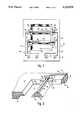
- FIG. 1is a plan view of a mass air flow sensor in accordance with a preferred embodiment of the invention
- FIG. 2is an enlarged perspective view, partially broken away, of the upper right thermal isolation zone area of the embodiment of FIG. 1;
- FIGS. 3, 4 and 5illustrate the fabrication of a mass air flow sensor in accordance with a preferred method of this invention. Specifically, FIG. 4 is a cross-sectional view taken through line 4--4 in FIG. 3 and FIG. 5 is cross-sectional view taken through line 5--5 in FIG. 3.
- a micromachined silicon monolithic mass air flow sensor 10is seen to comprise a generally planar silicon substrate 12 having an upper surface 14 and a lower surface 16.
- An air flow opening 18 through the silicon substrate 12is defined by an air flow opening perimeter 20.
- a first silicon member 22extends across the air flow opening from a first thermal isolation zone 24 to a second thermal isolation zone 26.
- the thermal isolation zones 24 and 26are seen to be opposite one another at the air flow opening perimeter 20.
- a second silicon member 28(shown in FIG. 1) is substantially identical to first silicon member 22. It extends across the air flow opening substantially parallel to first silicon member 22 from a third thermal isolation zone 30 to a fourth thermal isolation zone 32. Again, both the third and the fourth thermal isolation zones are located at the air flow opening perimeter 20.
- the porous silicon oxidepreferably is made to be essentially void free.
- the silicon members 22 and 28are trapezoidal in cross-section. As seen in FIG. 2, the bottom surface 34 of silicon member 22 is wider than top surface 36.
- the good thermal isolation provided by the thermal isolation zonesenables the use of larger cross-sectional area silicon members for improved durability while retaining good accuracy.
- good sensor accuracycan be achieved using silicon members which are more than 100 microns wide (width being the dimension of the top and bottom surface of the member perpendicular to the longitudinal axis).
- the beamis about 200 microns thick, the upper surface is 60 to 200 microns wide, the lower surface is 340 to 480 or more microns wide and the length (that is, the longitudinal dimension) is about 4 to 6 millimeters.
- the silicon memberneed not in all applications extend across the entire width of the air flow opening. Rather, in some embodiments of the invention the silicon member may be a beam extending from a thermal isolation zone at the perimeter of the air flow opening and having a free opposite end. Also, the silicon member may be square or rectangular in cross-section. Preferably, however, a trapezoidal shape is used, the thin film resistor (described below) being deposited on either the more narrow or wider surface and either facing the oncoming air flow or being on the leeward surface.
- the silicon members, the thermal isolation zones and the silicon substrateall have a co-planar upper surface.
- the lower surface 38 of the thermal isolation zoneis recessed from the lower surface 16 of the silicon substrate 12.
- the silicon beams 22 and 28are recessed even further, such that the silicon beams have less thickness (that is, vertical dimension) than the original silicon substrate.
- the silicon beamsare entirely discontiguous from the silicon substrate.
- the silicon beamsare integral with the thermal isolation zones which, in turn, are integral with the silicon substrate.
- the thermal isolation zone 24is seen to have a U-shaped configuration forming a recess 25.
- the recess of each thermal isolation zoneis open to the air flow opening and, more specifically, is open to, and aligned opposite, the recess of the opposite thermal isolation zone.
- a resistive thin film 40is formed on upper surface 36 of silicon member 22.
- a resistive thin film 42is formed on the upper surface of silicon member 28.
- the resistive thin filmmay be formed of any suitable material, a number of which are known to those skilled in the art of IC fabrication and MAFS fabrication. Nickel and platinum are preferred in view of their resistor properties and the ease with which they are deposited by well known metalization techniques.
- the resistorspreferably terminate at the end of the silicon members or in certain applications on the upper surface of the thermal isolation zone.
- Electrical connection means 44is provided for connecting the ends of the thin film resistors to circuitry connection sites for associated sensor circuitry. Such circuitry may be formed in or carried on the silicon substrate. It is not necessary, however, that the associated sensor circuitry be carried on-board the silicon substrate; it may be remote therefrom with electrical connection to the aforesaid electrical connection means 44.
- electrical connection means 44is seen to comprise a set of thin film leads, including specifically first electrical lead 46 extending on the upper surface 14 of the silicon substrate 12 from a wire bond pad 48 to electrical connection pad 49 making electrical connection with terminus 50 of thin film resistor 40.
- Wire bond pad 48is remote from the air flow opening 18.
- a second electrical lead 51is seen to extend on the surface 14 of silicon substrate 12 from electrical connection pad 55 making electrical connection with the second terminus 52 of thin film resistor 40, to a wire bond pad 54 remote from the air flow opening 18.
- a third electrical lead 56extends on the surface of the silicon substrate from electrical connection pad 61 making electrical connection with the first terminus 58 of the second thin film resistor 42 on the second silicon member 28 to a wire bond pad 60 remote from the air flow opening.
- a fourth electrical lead 62extends from electrical connection pad 67 making electrical connection with the second terminus 64 of thin film resistor 42, to a wire bond pad 66 remote from the air flow opening.
- the electrical leads 46, 50, 56 and 62, including their associated electrical connections and wire bond padspreferably are formed by any of the well known metalization techniques currently in commercial use for the production of mass air flow sensors, integrated circuits and the like.
- the leadsare either gold, preferably over a chromium adhesion layer, or aluminum. Alternative metals will be apparent to those skilled in the art in view of the present disclosure for particular applications in which the sensor is to be used.
- the U-shaped configuration shown in the drawings for the thermal isolation zonesis advantageous for several reasons.
- the thermal isolation zonescan be kept relatively small, preferably about 1 to 2 millimeters in width, to minimize stresses and for overall strength of the sensor component and its bowing characteristics. Further, it provides a high contact area between the silicon member and the porous silicon oxide material for good strength. It is generally preferable to use porous silicon oxide in thermal isolation zones embedded in a silicon substrate frame, as in the embodiment of FIGS. 1 and 2, rather than simply silicon beams attached to a porous silicon oxide frame, both for thermal uniformity along the frame and for strength.
- micromachined sensors in accordance with the inventionare fabricated by first providing a generally planar silicon substrate.
- the methodis carried out as a batch fabrication method wherein a plurality of micromachined sensor components are produced from a single silicon substrate wafer.
- Suitable silicon substrate wafersinclude commercially available wafers about 400 to 600 microns thick.
- a batch fabrication methodwill be described. It will be readily apparent to those skilled in the art from the present disclosure that the method steps are equally applicable for the fabrication of a single sensor component.
- porous silicon oxidehas been used, for example, for dielectric isolation in high temperature integrated circuits, as described in K. Imai, Solid State Electronics, 24, 159 (1981); K. Imai et al, IEEE Trans. Elec. Dev., ED-31, 297 (1984); and S. S. Tsao, IEEE Circuits and Devices Ma., November 1987, pg. 3, and references cited therein. Oxidation of porous silicon is described, for example, in T. Unagami, Jap.
- a protective maskis provided on the silicon substrate wafer.
- the protective maskis a silicon nitride coating grown on the lower surface and selectively on the upper surface of the wafer.
- Protective masks and coatings, and their formationare well known to those skilled in the art of sensor manufacture and IC manufacture.
- a layer of silicon oxidemay be provided under the silicon nitride protective mask.
- the upper surface of the waferis selectively protected, leaving unprotected a plurality of thermal isolation zone sites, preferably U-shaped surface areas, beneath which the thermal isolation zones will be formed as now described.
- a plurality of reduced density zonesare formed, such zones being located in pairs, each with its recess opened to, and aligned across from, the other zone in its pair.
- the density of the siliconis reduced, preferably, by electrochemical oxidation in hydrofluoric acid. It is within the ability of those skilled in the art to select current density and process duration to yield a desired silicon density and a desired depth for the reduced density zones.
- the siliconis reduced in density to about 0.4 that of the original silicon substrate wafer.
- Electrical contact to the siliconcan be made, for example, by a platinum metalization deposited on a small area of bare silicon on the wafer.
- the reduced density zonepreferably is formed to a depth equal to, or greater than, the intended depth of the silicon member such that the silicon member can be entirely discontiguous from the remainder of the silicon substrate.
- the reduced density zonesare then oxidized. Preferably they are exposed to an oxidizing atmosphere at elevated temperature to convert the porous silicon to porous silicon oxide.
- the thermal conductivity of porous silicon oxideis small compared to that of the original silicon substrate.
- the oxidation processalso acts as a densification process, since the silicon in the reduced density zone expands in volume as it is transformed to silicon oxide.
- the resulting thermal isolation zonesare, therefore, relatively strong.
- the structureis preferably relatively stress free. This can be achieved by controlling the oxidation process to yield porous silicon oxide which is substantially void free.
- the resulting thermal isolation zonesin accordance with preferred embodiments of the invention, are smooth on the surface; continuous metal films can be deposited thereon.
- the waferis further processed to form the final sensor component structure.
- Such further processing stepspreferably follow essentially the method described in U.S. Pat. No. 4,594,889 to McCarthy, the disclosure of which is incorporated herein by reference.
- Such stepsare well known in the field of silicon sensor fabrication and IC manufacture.
- the upper surface of the silicon substrate waferis selectively metalized to form a plurality of thin film resistors.
- resistorspreferably are formed of platinum or nickel, each extending on the upper surface of the wafer between a pair of thermal isolation zones.
- the resistorspreferably are fabricated by sputter deposition, photo lithography and chemical etch or by electron beam deposition, photo lithography and wet etch.
- the resistor widthpreferably is kept smaller than that of the recess in the thermal isolation zone to ensure that, after etching the silicon, each resistor rests fully on its silicon beam support.
- Electrical connection meansare formed on the upper surface of the wafer, preferably comprising either gold over a chromium adhesion layer or aluminum.
- the metalization step for forming such electrical connection meansfollows techniques well known to those skilled in the art.
- the metal layersthen are passivated to protect them during subsequent processing steps. Passivation can be by silicon nitride, for example, plasma enhanced chemical vapor deposited silicon nitride.
- the passivation on the silicon wafersis subsequently selectively stripped, for example, by lithography and plasma etching, to allow formation of the air flow openings and silicon members, preferably by double-sided etching, preferably anisotropic etching by EDP or the like.
- the porous silicon oxideis substantially unaffected by anisotropic EDP silicon etch. Etching from both sides produces silicon members whose thickness is approximately half that of the original silicon wafer.
- beams of different thicknessescan be obtained by a timed etch, passivation of one surface (for instance, the bottom surface for beams thicker than half the wafer thickness), and/or continuation of the etch after breakthrough as described in U.S. Pat. No. 4,771,271 to Zanini-Fisher, the disclosure of which is incorporated herein by reference.
- the resulting structurehas silicon members extending across an air flow opening, wherein the silicon members are attached at both ends to porous silicon oxide thermal isolation zones.
- a sensor 100shown partially broken away, is seen to comprise a silicon substrate 110 having an air flow opening 112 formed therethrough.
- Silicon member 114bridges across the air flow opening 112 from a first thermal isolation zone 116 on the right side of the air flow opening 112 to a second thermal isolation zone 118 on the opposite side of the air flow opening 112.
- the two thermal isolation zones 116, 118are formed of porous silicon oxide in accordance with the present invention, as described above.
- the silicon substrate 110 and the silicon member 114are formed of silicon, both integral with the thermal isolation zone, but discontiguous from each other.
- a silicon nitride protective coating 120selectively covers the upper surface
- a silicon nitride protective coating 122selectively covers the lower surface.
- the silicon member 114has a first end portion 122 received in a recess 124 formed by the U-shaped thermal isolation zone 116. Similarly, opposite end portion 126 of silicon member 114 is received in recess 128 of thermal isolation zone 118.
- the etched assemblyis subsequently divided into individual sensor components.
Landscapes
- Physics & Mathematics (AREA)
- Fluid Mechanics (AREA)
- General Physics & Mathematics (AREA)
- Measuring Volume Flow (AREA)
- Micromachines (AREA)
Abstract
Description
Claims (11)
Priority Applications (1)
| Application Number | Priority Date | Filing Date | Title |
|---|---|---|---|
| US07/812,397US5231878A (en) | 1991-12-23 | 1991-12-23 | Mass air flow sensor |
Applications Claiming Priority (1)
| Application Number | Priority Date | Filing Date | Title |
|---|---|---|---|
| US07/812,397US5231878A (en) | 1991-12-23 | 1991-12-23 | Mass air flow sensor |
Publications (1)
| Publication Number | Publication Date |
|---|---|
| US5231878Atrue US5231878A (en) | 1993-08-03 |
Family
ID=25209441
Family Applications (1)
| Application Number | Title | Priority Date | Filing Date |
|---|---|---|---|
| US07/812,397Expired - LifetimeUS5231878A (en) | 1991-12-23 | 1991-12-23 | Mass air flow sensor |
Country Status (1)
| Country | Link |
|---|---|
| US (1) | US5231878A (en) |
Cited By (26)
| Publication number | Priority date | Publication date | Assignee | Title |
|---|---|---|---|---|
| US5396795A (en)* | 1991-12-09 | 1995-03-14 | Mitsubishi Denki Kabushiki Kaisha | Semiconductor sensor device for measuring intake flow rate |
| US5451371A (en)* | 1994-06-09 | 1995-09-19 | Ford Motor Company | High-sensitivity, silicon-based, microcalorimetric gas sensor |
| US5708205A (en)* | 1995-05-19 | 1998-01-13 | Hitachi, Ltd. | Measuring element for a mass air flow sensor and mass air flow sensor using the measuring element |
| US5726357A (en)* | 1993-06-07 | 1998-03-10 | Ricoh Seiki Company, Ltd. | Flow sensor |
| WO1998050763A1 (en)* | 1997-05-07 | 1998-11-12 | Ncsr 'demokritos' | Integrated gas flow sensor based on porous silicon micromachining |
| RU2122181C1 (en)* | 1994-03-04 | 1998-11-20 | Роберт Бош Гмбх | Device for measuring of flowing medium mass |
| US6393907B1 (en)* | 1999-03-24 | 2002-05-28 | Mitsubishi Denki Kabushiki Kaisha | Thermo-sensitive flow rate sensor |
| WO2002042723A1 (en)* | 2000-11-23 | 2002-05-30 | Robert Bosch Gmbh | Flow sensor |
| DE10117486A1 (en)* | 2001-04-07 | 2002-10-17 | Bosch Gmbh Robert | Method for producing a semiconductor component and a semiconductor component produced using the method |
| EP1306349A1 (en)* | 2001-10-24 | 2003-05-02 | Robert Bosch Gmbh | Method of manufacture of an array of membrane sensors and array of membrane sensors |
| DE10161202C1 (en)* | 2001-12-13 | 2003-05-08 | Bosch Gmbh Robert | Reducing the thickness of a silicon substrate which has been made porous comprises making porous the rear side of the substrate lying opposite a front side which has been made porous, then removing the porous material formed |
| US6631638B2 (en) | 2001-01-30 | 2003-10-14 | Rosemount Aerospace Inc. | Fluid flow sensor |
| WO2002084748A3 (en)* | 2001-04-14 | 2003-12-04 | Bosch Gmbh Robert | Method for producing optically transparent regions in a silicon substrate |
| US6708561B2 (en) | 2002-04-19 | 2004-03-23 | Visteon Global Technologies, Inc. | Fluid flow meter having an improved sampling channel |
| US20040055375A1 (en)* | 2002-09-20 | 2004-03-25 | Visteon Global Technologies, Inc. | Mass fluid flow sensor having an improved housing design |
| US20040163460A1 (en)* | 2003-02-24 | 2004-08-26 | Visteon Global Technologies, Inc. | Hot-wire mass flow sensor with low-loss bypass passage |
| WO2004071944A1 (en)* | 2003-02-14 | 2004-08-26 | Robert Bosch Gmbh | Method for the production of a component comprising a semiconductor carrier and component |
| US20040201075A1 (en)* | 2003-04-09 | 2004-10-14 | Thurgood Blaine J. | Semiconductor die configured for use with interposer substrates having reinforced interconnect slots |
| US20080053215A1 (en)* | 2006-08-31 | 2008-03-06 | Hitachi, Ltd. | Thermal Type Gas Flow Meter |
| DE102008020874A1 (en) | 2008-04-25 | 2009-11-12 | Eads Deutschland Gmbh | Flow or eddy sensor for measurement of vector speed, has hot wire sensor element micro-manufactured on substrate for measurement of component of flow or cyclic field of fluid |
| DE10046621B4 (en)* | 2000-09-20 | 2010-08-05 | Robert Bosch Gmbh | Method for producing a membrane sensor array and membrane sensor array |
| US8148696B2 (en) | 2001-11-30 | 2012-04-03 | SNC Holdings Corp. | Single-use external dosimeters for use in radiation therapies and related devices and computer program products |
| US20120192645A1 (en)* | 2009-12-18 | 2012-08-02 | Honeywell International Inc. | Flow sensors having nanoscale coating for corrosion resistance |
| US20120240674A1 (en)* | 2011-03-25 | 2012-09-27 | Hitachi Automotive Systems, Ltd. | Thermal fluid flow sensor and method of manufacturing the same |
| US20180274958A1 (en)* | 2017-03-22 | 2018-09-27 | A. O. Smith Corporation | Flow sensor with hot film anemometer |
| US10151772B2 (en) | 2015-01-23 | 2018-12-11 | Embry-Riddle Aeronautical Univeristy, Inc. | Hot wire anemometer |
Citations (8)
| Publication number | Priority date | Publication date | Assignee | Title |
|---|---|---|---|---|
| US4472239A (en)* | 1981-10-09 | 1984-09-18 | Honeywell, Inc. | Method of making semiconductor device |
| US4594889A (en)* | 1984-12-06 | 1986-06-17 | Ford Motor Company | Mass airflow sensor |
| US4680963A (en)* | 1985-01-24 | 1987-07-21 | Kabushiki Kaisha Toyota Chuo Kenkyusho | Semiconductor flow velocity sensor |
| US4771271A (en)* | 1987-03-11 | 1988-09-13 | Ford Motor Company | Silicon based low level liquid sensor having a fast response time |
| US4808549A (en)* | 1988-05-27 | 1989-02-28 | Ford Motor Company | Method for fabricating a silicon force transducer |
| WO1989003512A1 (en)* | 1987-10-14 | 1989-04-20 | Rosemount Inc. | Fluid flow detector |
| US4843445A (en)* | 1985-05-21 | 1989-06-27 | Swema Instrument Aktiebolag | Integrated semiconductor circuit and method for producing it, and use of such a circuit for providing a flow meter |
| US4870860A (en)* | 1985-02-14 | 1989-10-03 | Nippon Soken, Inc. | Direct-heated flow measuring apparatus having improved response characteristics |
- 1991
- 1991-12-23USUS07/812,397patent/US5231878A/ennot_activeExpired - Lifetime
Patent Citations (8)
| Publication number | Priority date | Publication date | Assignee | Title |
|---|---|---|---|---|
| US4472239A (en)* | 1981-10-09 | 1984-09-18 | Honeywell, Inc. | Method of making semiconductor device |
| US4594889A (en)* | 1984-12-06 | 1986-06-17 | Ford Motor Company | Mass airflow sensor |
| US4680963A (en)* | 1985-01-24 | 1987-07-21 | Kabushiki Kaisha Toyota Chuo Kenkyusho | Semiconductor flow velocity sensor |
| US4870860A (en)* | 1985-02-14 | 1989-10-03 | Nippon Soken, Inc. | Direct-heated flow measuring apparatus having improved response characteristics |
| US4843445A (en)* | 1985-05-21 | 1989-06-27 | Swema Instrument Aktiebolag | Integrated semiconductor circuit and method for producing it, and use of such a circuit for providing a flow meter |
| US4771271A (en)* | 1987-03-11 | 1988-09-13 | Ford Motor Company | Silicon based low level liquid sensor having a fast response time |
| WO1989003512A1 (en)* | 1987-10-14 | 1989-04-20 | Rosemount Inc. | Fluid flow detector |
| US4808549A (en)* | 1988-05-27 | 1989-02-28 | Ford Motor Company | Method for fabricating a silicon force transducer |
Non-Patent Citations (16)
| Title |
|---|
| C. H. Stephan and M. Zanini, A Micromachined, Silicon Mass Air Flow Sensor For Automotive Applications ; (undated).* |
| C. H. Stephan and M. Zanini, A Micromachined, Silicon Mass-Air-Flow Sensor For Automotive Applications; (undated). |
| Ford Motor Company Technical Report No. SR 89 160 Functional Behavior of a Batch Fabrication Monolithic Silicon Mass Air Flow Sensor , C. H. Stephan, Jan. 23, 1990.* |
| Ford Motor Company Technical Report No. SR 89-160 Functional Behavior of a Batch-Fabrication Monolithic Silicon Mass Air Flow Sensor, C. H. Stephan, Jan. 23, 1990. |
| IEEE Publication No. 0018 9383/86/1000 1470 1.00 A Monolithic Gas Flow Sensor with Polyimide as Thermal Insulator , Goran N. Stemme, IEEE Transactions on Electron Devices , vol. ED 33, No. 10, Oct. 1986.* |
| IEEE Publication No. 0018-9383/86/1000-1470§1.00 "A Monolithic Gas Flow Sensor with Polyimide as Thermal Insulator", Goran N. Stemme, IEEE Transactions on Electron Devices, vol. ED-33, No. 10, Oct. 1986. |
| Imai, Kazuo et al., "FIPOS (Full Isolation by Porous Oxidized Silicon Technology and Its Application to LSI's," IEEE Transactions on Electron Devices, vol. ED-31, No. 3, Mar. 1984, pp. 297-302. |
| Imai, Kazuo et al., FIPOS (Full Isolation by Porous Oxidized Silicon Technology and Its Application to LSI s, IEEE Transactions on Electron Devices , vol. ED 31, No. 3, Mar. 1984, pp. 297 302.* |
| Imai, Kazuo, "A New Dielectric Isolation Method Using Porous Silicon," Solid-State Electronics, vol. 24, (1981) pp. 159-164. |
| Imai, Kazuo, A New Dielectric Isolation Method Using Porous Silicon, Solid State Electronics , vol. 24, (1981) pp. 159 164.* |
| Smith, R. L. et al., "An Integrated Sensor for Electrochemical Measurements," IEEE Transactions on Biomedical Engineering, vol. BME-33, No. 2, Feb. 1986, pp. 83-90. |
| Smith, R. L. et al., An Integrated Sensor for Electrochemical Measurements, IEEE Transactions on Biomedical Engineering , vol. BME 33, No. 2, Feb. 1986, pp. 83 90.* |
| Tabata, Osamu, "Fast-Response Silicon Flow Sensor with an On-Chip Fluid Temperature Sensing Element," IEEE Transactions on Electron Devices, vol. ED-33, No. 3, Mar. 1986, pp. 361-365. |
| Tabata, Osamu, Fast Response Silicon Flow Sensor with an On Chip Fluid Temperature Sensing Element, IEEE Transactions on Electron Devices , vol. ED 33, No. 3, Mar. 1986, pp. 361 365.* |
| Unagami, Takashi, "Oxidation of Porous Silicon and Properties of Its Oxide Film," Japanese Journal of Applied Physics, vol. 19, No. 2, Feb. 1980, pp. 231-241. |
| Unagami, Takashi, Oxidation of Porous Silicon and Properties of Its Oxide Film, Japanese Journal of Applied Physics , vol. 19, No. 2, Feb. 1980, pp. 231 241.* |
Cited By (48)
| Publication number | Priority date | Publication date | Assignee | Title |
|---|---|---|---|---|
| US5396795A (en)* | 1991-12-09 | 1995-03-14 | Mitsubishi Denki Kabushiki Kaisha | Semiconductor sensor device for measuring intake flow rate |
| US5726357A (en)* | 1993-06-07 | 1998-03-10 | Ricoh Seiki Company, Ltd. | Flow sensor |
| RU2122181C1 (en)* | 1994-03-04 | 1998-11-20 | Роберт Бош Гмбх | Device for measuring of flowing medium mass |
| US5451371A (en)* | 1994-06-09 | 1995-09-19 | Ford Motor Company | High-sensitivity, silicon-based, microcalorimetric gas sensor |
| US5801070A (en)* | 1994-06-09 | 1998-09-01 | Ford Global Technologies, Inc. | High sensitivity, silicon-based, Microcalorimetric gas sensor and fabrication method |
| US5708205A (en)* | 1995-05-19 | 1998-01-13 | Hitachi, Ltd. | Measuring element for a mass air flow sensor and mass air flow sensor using the measuring element |
| WO1998050763A1 (en)* | 1997-05-07 | 1998-11-12 | Ncsr 'demokritos' | Integrated gas flow sensor based on porous silicon micromachining |
| US6393907B1 (en)* | 1999-03-24 | 2002-05-28 | Mitsubishi Denki Kabushiki Kaisha | Thermo-sensitive flow rate sensor |
| DE10046621B4 (en)* | 2000-09-20 | 2010-08-05 | Robert Bosch Gmbh | Method for producing a membrane sensor array and membrane sensor array |
| WO2002042723A1 (en)* | 2000-11-23 | 2002-05-30 | Robert Bosch Gmbh | Flow sensor |
| US7040160B2 (en) | 2000-11-23 | 2006-05-09 | Robert Bosch Gmbh | Flow sensor |
| US20040069626A1 (en)* | 2000-11-23 | 2004-04-15 | Hans Artmann | Flow sensor |
| US6631638B2 (en) | 2001-01-30 | 2003-10-14 | Rosemount Aerospace Inc. | Fluid flow sensor |
| US20040147057A1 (en)* | 2001-04-07 | 2004-07-29 | Hubert Benzel | Method for producing a semiconductor component and a semiconductor component produced according to this method |
| DE10117486A1 (en)* | 2001-04-07 | 2002-10-17 | Bosch Gmbh Robert | Method for producing a semiconductor component and a semiconductor component produced using the method |
| US7160750B2 (en) | 2001-04-07 | 2007-01-09 | Robert Bosch Gmbh | Method of producing a semiconductor sensor component |
| US20040155010A1 (en)* | 2001-04-14 | 2004-08-12 | Hubert Benzel | Method for producing optically transparent regions in a silicon substrate |
| WO2002084748A3 (en)* | 2001-04-14 | 2003-12-04 | Bosch Gmbh Robert | Method for producing optically transparent regions in a silicon substrate |
| US7419581B2 (en) | 2001-04-14 | 2008-09-02 | Robert Bosch Gmbh | Method for producing optically transparent regions in a silicon substrate |
| EP1306349A1 (en)* | 2001-10-24 | 2003-05-02 | Robert Bosch Gmbh | Method of manufacture of an array of membrane sensors and array of membrane sensors |
| US8148696B2 (en) | 2001-11-30 | 2012-04-03 | SNC Holdings Corp. | Single-use external dosimeters for use in radiation therapies and related devices and computer program products |
| DE10161202C1 (en)* | 2001-12-13 | 2003-05-08 | Bosch Gmbh Robert | Reducing the thickness of a silicon substrate which has been made porous comprises making porous the rear side of the substrate lying opposite a front side which has been made porous, then removing the porous material formed |
| US6708561B2 (en) | 2002-04-19 | 2004-03-23 | Visteon Global Technologies, Inc. | Fluid flow meter having an improved sampling channel |
| US20040055375A1 (en)* | 2002-09-20 | 2004-03-25 | Visteon Global Technologies, Inc. | Mass fluid flow sensor having an improved housing design |
| US6826955B2 (en) | 2002-09-20 | 2004-12-07 | Visteon Global Technologies, Inc. | Mass fluid flow sensor having an improved housing design |
| US7803646B2 (en) | 2003-02-14 | 2010-09-28 | Robert Bosch Gmbh | Method for producing a component having a semiconductor substrate and component |
| US20060258037A1 (en)* | 2003-02-14 | 2006-11-16 | Robert Bosch Gmbh | Method for producing a component having a semiconductor substrate and component |
| WO2004071944A1 (en)* | 2003-02-14 | 2004-08-26 | Robert Bosch Gmbh | Method for the production of a component comprising a semiconductor carrier and component |
| US6973825B2 (en) | 2003-02-24 | 2005-12-13 | Visteon Global Technologies, Inc. | Hot-wire mass flow sensor with low-loss bypass passage |
| US20040163460A1 (en)* | 2003-02-24 | 2004-08-26 | Visteon Global Technologies, Inc. | Hot-wire mass flow sensor with low-loss bypass passage |
| US20040201075A1 (en)* | 2003-04-09 | 2004-10-14 | Thurgood Blaine J. | Semiconductor die configured for use with interposer substrates having reinforced interconnect slots |
| US7078823B2 (en) | 2003-04-09 | 2006-07-18 | Micron Technology, Inc. | Semiconductor die configured for use with interposer substrates having reinforced interconnect slots |
| US7102217B2 (en)* | 2003-04-09 | 2006-09-05 | Micron Technology, Inc. | Interposer substrates with reinforced interconnect slots, and semiconductor die packages including same |
| US20040200063A1 (en)* | 2003-04-09 | 2004-10-14 | Thurgood Blaine J. | Interposer substrates with multi-segment interconnect slots, semiconductor die packages including same, semiconductor dice for use therewith and methods of fabrication |
| US20040201111A1 (en)* | 2003-04-09 | 2004-10-14 | Thurgood Blaine J. | Interposer substrates with multisegment interconnect slots, semiconductor die packages including same, semiconductor dice for use therewith and methods of fabrication |
| US20080053215A1 (en)* | 2006-08-31 | 2008-03-06 | Hitachi, Ltd. | Thermal Type Gas Flow Meter |
| US7437927B2 (en)* | 2006-08-31 | 2008-10-21 | Hitachi, Ltd. | Thermal type gas flow meter |
| DE102008020874B4 (en)* | 2008-04-25 | 2010-02-25 | Eads Deutschland Gmbh | Flow or vortex sensor |
| DE102008020874A1 (en) | 2008-04-25 | 2009-11-12 | Eads Deutschland Gmbh | Flow or eddy sensor for measurement of vector speed, has hot wire sensor element micro-manufactured on substrate for measurement of component of flow or cyclic field of fluid |
| US20120192645A1 (en)* | 2009-12-18 | 2012-08-02 | Honeywell International Inc. | Flow sensors having nanoscale coating for corrosion resistance |
| US8424380B2 (en)* | 2009-12-18 | 2013-04-23 | Honeywell International Inc. | Flow sensors having nanoscale coating for corrosion resistance |
| US20120240674A1 (en)* | 2011-03-25 | 2012-09-27 | Hitachi Automotive Systems, Ltd. | Thermal fluid flow sensor and method of manufacturing the same |
| US8714008B2 (en)* | 2011-03-25 | 2014-05-06 | Hitachi Automotive Systems, Ltd. | Thermal fluid flow sensor and method of manufacturing the same |
| US9379302B2 (en) | 2011-03-25 | 2016-06-28 | Hitachi Automotive Systems, Ltd. | Method of manufacturing the thermal fluid flow sensor |
| US10151772B2 (en) | 2015-01-23 | 2018-12-11 | Embry-Riddle Aeronautical Univeristy, Inc. | Hot wire anemometer |
| US20180274958A1 (en)* | 2017-03-22 | 2018-09-27 | A. O. Smith Corporation | Flow sensor with hot film anemometer |
| US10274353B2 (en)* | 2017-03-22 | 2019-04-30 | A. O. Smith Corporation | Flow sensor with hot film anemometer |
| US10598530B2 (en) | 2017-03-22 | 2020-03-24 | A. O. Smith Corporation | Flow sensor with hot film anemometer |
Similar Documents
| Publication | Publication Date | Title |
|---|---|---|
| US5231878A (en) | Mass air flow sensor | |
| EP0393141B1 (en) | Silicon-based mass airflow sensor | |
| JP2757259B2 (en) | Intermediate structure of thin film microsensor for flow velocity measurement and method of manufacturing the same | |
| US4594889A (en) | Mass airflow sensor | |
| US5597957A (en) | Microvacuum sensor having an expanded sensitivity range | |
| US6184773B1 (en) | Rugged fluid flow and property microsensor | |
| Dibbern | A substrate for thin-film gas sensors in microelectronic technology | |
| US7255001B1 (en) | Thermal fluid flow sensor and method of forming same technical field | |
| US6139758A (en) | Method of manufacturing a micromachined thermal flowmeter | |
| JP3542614B2 (en) | Temperature sensor and method for manufacturing the temperature sensor | |
| US5006421A (en) | Metalization systems for heater/sensor elements | |
| US5313832A (en) | Composite mass air flow sensor | |
| JP3333712B2 (en) | Flow rate detecting element and flow rate sensor using the same | |
| US4633578A (en) | Miniature thermal fluid flow sensors and batch methods of making same | |
| US4733559A (en) | Thermal fluid flow sensing method and apparatus for sensing flow over a wide range of flow rates | |
| JP2005505758A (en) | Micromachining type thermal conductivity sensor with porous cover | |
| EP1333255B1 (en) | Flow sensor | |
| JP3455473B2 (en) | Thermal flow sensor | |
| JPH1123338A (en) | Thermosensitive flow rate detecting element and flow rate sensor using the same | |
| US20030019290A1 (en) | Flow sensor | |
| US6378365B1 (en) | Micromachined thermal flowmeter having heating element disposed in a silicon island | |
| US4561303A (en) | Mass airflow sensor with backflow detection | |
| KR100544772B1 (en) | A thermosensitive flow rate detecting element and method for the manufacture thereof | |
| US5783854A (en) | Thermally isolated integrated circuit | |
| JP2005077343A (en) | Flow sensor |
Legal Events
| Date | Code | Title | Description |
|---|---|---|---|
| AS | Assignment | Owner name:FORD MOTOR COMPANY, MICHIGAN Free format text:ASSIGNMENT OF ASSIGNORS INTEREST.;ASSIGNORS:ZANINI-FISHER, MARGHERITA;STEPHAN, CRAIG H.;REEL/FRAME:006031/0244 Effective date:19911213 | |
| STCF | Information on status: patent grant | Free format text:PATENTED CASE | |
| FEPP | Fee payment procedure | Free format text:PAYOR NUMBER ASSIGNED (ORIGINAL EVENT CODE: ASPN); ENTITY STATUS OF PATENT OWNER: LARGE ENTITY | |
| FPAY | Fee payment | Year of fee payment:4 | |
| SULP | Surcharge for late payment | ||
| FPAY | Fee payment | Year of fee payment:8 | |
| AS | Assignment | Owner name:FORD GLOBAL TECHNOLOGIES, INC. A MICHIGAN CORPORAT Free format text:ASSIGNMENT OF ASSIGNORS INTEREST;ASSIGNOR:FORD MOTOR COMPANY, A DELAWARE CORPORATION;REEL/FRAME:011467/0001 Effective date:19970301 | |
| AS | Assignment | Owner name:REGENTS OF THE UNIVERSITY OF MICHIGAN, MICHIGAN Free format text:ASSIGNMENT OF ASSIGNORS INTEREST;ASSIGNOR:FORD GLOBAL TECHNOLOGIES, INC.;REEL/FRAME:012365/0278 Effective date:20011102 | |
| FPAY | Fee payment | Year of fee payment:12 |