US5231590A - Technique for modifying an integrated circuit layout - Google Patents
Technique for modifying an integrated circuit layoutDownload PDFInfo
- Publication number
- US5231590A US5231590AUS07/420,912US42091289AUS5231590AUS 5231590 AUS5231590 AUS 5231590AUS 42091289 AUS42091289 AUS 42091289AUS 5231590 AUS5231590 AUS 5231590A
- Authority
- US
- United States
- Prior art keywords
- layout
- database
- circuit
- integrated circuit
- modified
- Prior art date
- Legal status (The legal status is an assumption and is not a legal conclusion. Google has not performed a legal analysis and makes no representation as to the accuracy of the status listed.)
- Expired - Lifetime
Links
Images


Classifications
- G—PHYSICS
- G06—COMPUTING OR CALCULATING; COUNTING
- G06F—ELECTRIC DIGITAL DATA PROCESSING
- G06F30/00—Computer-aided design [CAD]
- G06F30/30—Circuit design
- G06F30/39—Circuit design at the physical level
- G—PHYSICS
- G06—COMPUTING OR CALCULATING; COUNTING
- G06F—ELECTRIC DIGITAL DATA PROCESSING
- G06F30/00—Computer-aided design [CAD]
- G06F30/30—Circuit design
- G06F30/39—Circuit design at the physical level
- G06F30/398—Design verification or optimisation, e.g. using design rule check [DRC], layout versus schematics [LVS] or finite element methods [FEM]
Definitions
- This inventionrelates generally to techniques of integrated electronic circuit design, and particularly to a process of modifying or revising an existing integrated circuit layout.
- the steps required in order to design masks used to form the various layers on an integrated electronic circuitare many.
- the first major step, after defining what the circuit is to do,is to prepare a schematic diagram showing all of the circuit elements and their interconnections.
- the function of the circuitis then tested by computer simulation of expected operating conditions.
- a net list of the circuit schematicis developed.
- a net listdescribes the schematic diagram by assigning a unique number to each digital logic gate or other circuit component, and a separate identification for each terminal of the component.
- the schematic diagramis then expressed as a net list of interconnections among the identified gate terminals and input/output points of the circuit.
- the schematic circuitis then converted to a circuit layout by designing a number of masks which, when used to make an integrated circuit chip, implements the circuit initially designed as a schematic diagram. This is accomplished by a layout designer with the help of sophisticated computer programs. When the designer has completed the layout work, a net list is extracted from the resulting layout computer data by a commercially available net list extraction computer software program. This net list is then compared with the original schematic net list as a check on whether the layout was done properly. This comparison is accomplished by a commercially available net list comparison computer software program which gives an output that identifies the differences in the net list. The layout designer can then use a layout editing computer software program to modify the layout database in order to eliminate any differences. The process identifies mask layout errors without first having to make an actual integrated circuit.
- an existing integrated circuit layout computer databaseis initially run through a net list extractor computer software program to obtain a net list of the electronic circuit that is implemented by the layout.
- the modified databaseis run through the same extractor program to obtain a net list of the circuit of the modified layout.
- These net listsare then compared by the use of available computer software. If there are any differences in the net lists, then the layout designer proceeds to edit the layout database to correct the errors that were made in the original modification of the database. After editing, a net list of the edited modified layout is then compared with the original net list. If any errors remain, the layout may be again edited, the net list compared and so on. This technique results in verification that a modified circuit layout still implements the same circuit functions as did the original layout, in an efficient and cost effective manner.
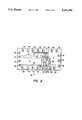
- FIG. 1Aillustrates an example integrated circuit chip layout which is to be modified
- FIG. 1Billustrates an example modified integrated circuit layout of FIG. 1A
- FIG. 2is an integrated circuit layout that shows another example modification of the layout of FIG. 1A.
- FIG. 3is a flow diagram that illustrates the improved process of the present invention in order to verify such modifications.
- FIG. 1AAn example digital integrated circuit layout is outlined in FIG. 1A.
- An integrated circuit chip 11can function as a microprocessor, as one of many types of computer peripheral chips, as a digital memory, and the like. The techniques being described are not limited to any particular type of digital circuit.
- the layout of the chip 11can be considered to have two major components.
- a first component 13is a pad ring, a region around the outside perimeter of the chip that includes a plurality of connection pads 21-36.
- a major portion of the operating circuitis contained in a region 15 in the middle of the chip layout.
- the size of the layout, number of connection pads, and similar physical characteristicswill vary considerably from chip to chip, depending upon its function, purpose and complexity.
- Such a reduction in sizerequires more than a mere demagnification of the various masks that are used to manufacture the circuits.
- Some modification of the circuit layoutis usually required in order to affect a shrink, that modification usually being in the region of the pad ring 13. That is because the physical size of the pads themselves generally must remain the same, or cannot be shrunk as much as the rest of the circuit.
- Such a shrink of the FIG. 1A layoutis shown in FIG. 1B where similar elements are identified by the same reference numbers but with a prime (') added. Enough pad area must remain for effecting a physical contact with a conductor that connects that pad with an external pin of a package in which the circuit chip is mounted.
- Integrated circuit packaging technologyis not allowing the pads to be reduced in size as much as process technology is allowing the remaining portions of the circuit to be shrunk. The result is that circuit elements in the pad ring 13 must be rearranged in order to accommodate the relatively larger size pads that result after the overall circuit layout size is reduced.
- circuit elements in the pad ring area 13can be updated, examples of this being in connection with e ectrostatic discharge protection circuits provided with each pad and any CMOS latch-up circuits. This allows any improvements in technology of these types of circuits to be incorporated into the new chip.
- FIG. 2illustrates the combining of the circuit 11 with another circuit 17 to form a single chip 19.
- Such combinationsare becoming quite popular in order to provide integrated circuits for specific applications.
- the circuit layout 11is of a microprocessor, it can be combined with a layout 17 for an input/output circuit or a math co-processor.
- Such functionshave been most commonly provided on separate integrated circuit chips.
- theycan be combined into a single chip, the total number of I.C. packages required for a given electronic system is reduced.
- these additional changesare accomplished by adding another metal layer to the structure of the chip so that various interconnections may be made without having to disturb the layout of the remaining layers of the chip. This can easily be done where the layout design of the circuit 11 has been accomplished with only a single metal layer.
- This additional metal layeris used to extend the pad 34 to another pad 38 at an edge of the circuit chip 19 by a wide conductor 51.
- pad 35is moved to a position 39 by a conductor 53.
- the pads of the circuit 11 along the edge adjacent the new circuit 17need not all be moved into the circuit area 17, however, but can be moved to locations along the remaining outside edges of the circuit 11 by rearranging its pads.
- the pad 36being moved to a new pad location 37 and interconnected with a conductor 55.
- the pads 26, 27 and 28have to be moved. This movement causes significant rearrangement of circuit elements formed by other layers of the layout 11, and thus introduces the possibility of inadvertent changes in the circuit schematic being made by this operation.
- the conductors 51, 53 and 55are made to be relatively wide, in this example, since they are carrying output signals.
- the new circuit 17In addition to moving these pads, some or all of the pads of the circuit 11 need to be electrically extended into and connected with portions of the new circuit 17. Three such interconnections are shown being made by this new metal layer, namely by conductors 57, 59 and 61. And, of course, the new circuit 17 has its own pads 40-44 that must be provided around the outside edge of the layout 19.
- FIG. 3a process is utilized with such existing circuits, using available computer program software tools, to allow such verification as part of editing an existing layout. This process is illustrated in FIG. 3, in the form of a flow diagram.
- the layout database for the circuit 11is initially run through net list extractor software in order to obtain a net list of the circuit implemented by the layout before any editing of the layout occurs. This is illustrated in FIG. 3 by steps 71 and 73.
- a first step 71involves assigning specific designations to the various input and output connections of the circuit 11. These designations are then inputted into the net list extractor software that is run in step 73.
- a next step 75is the editing of the layout from the original layout computer database.
- a standard layout editing software packageis used in this process. This is the point at which the circuit element rearrangements, addition of other layers, etc., of the circuit layout 11 are accomplished.
- a next step 77is to run the edited layout database through the net list extractor software again. This results in a net list of the edited layout which is then, in a step 79, compared to the net list obtained in step 73.
- This comparisonis accomplished by using an existing net list comparison computer software package. Before comparison, however, it may be desirable to alter the databases somewhat to eliminate portions of the layout which are not part of the circuit being implemented, such as company logo, test circuits, alignment keys and the like.
- step 79The results of the comparison of step 79 give a list of any differences in the two net lists. If there are no differences that relate to the circuit being implemented, as reviewed at a decision point 81, the edited layout database is then known to be free of any inadvertent errors made in the schematic diagram during the editing process.
- a next step 83is to utilize this edited database to make the plurality of masks that are used in the process of making the integrated circuit on a silicon wafer.
- step 81it is determined that some errors have been introduced into the layout, the exact nature of each error is investigated and corrected in a step 85 by further use of the layout editor computer software package. Once the corrections are made, steps 77 and 79 are again performed on the corrected edited layout database.
Landscapes
- Engineering & Computer Science (AREA)
- Computer Hardware Design (AREA)
- Physics & Mathematics (AREA)
- Theoretical Computer Science (AREA)
- Evolutionary Computation (AREA)
- Geometry (AREA)
- General Engineering & Computer Science (AREA)
- General Physics & Mathematics (AREA)
- Design And Manufacture Of Integrated Circuits (AREA)
- Semiconductor Integrated Circuits (AREA)
Abstract
Description
Claims (6)
Priority Applications (1)
| Application Number | Priority Date | Filing Date | Title |
|---|---|---|---|
| US07/420,912US5231590A (en) | 1989-10-13 | 1989-10-13 | Technique for modifying an integrated circuit layout |
Applications Claiming Priority (1)
| Application Number | Priority Date | Filing Date | Title |
|---|---|---|---|
| US07/420,912US5231590A (en) | 1989-10-13 | 1989-10-13 | Technique for modifying an integrated circuit layout |
Publications (1)
| Publication Number | Publication Date |
|---|---|
| US5231590Atrue US5231590A (en) | 1993-07-27 |
Family
ID=23668350
Family Applications (1)
| Application Number | Title | Priority Date | Filing Date |
|---|---|---|---|
| US07/420,912Expired - LifetimeUS5231590A (en) | 1989-10-13 | 1989-10-13 | Technique for modifying an integrated circuit layout |
Country Status (1)
| Country | Link |
|---|---|
| US (1) | US5231590A (en) |
Cited By (57)
| Publication number | Priority date | Publication date | Assignee | Title |
|---|---|---|---|---|
| US5308798A (en)* | 1992-11-12 | 1994-05-03 | Vlsi Technology, Inc. | Preplacement method for weighted net placement integrated circuit design layout tools |
| US5349542A (en)* | 1992-04-02 | 1994-09-20 | Vlsi Technology, Inc. | Method for sizing widths of power busses in integrated circuits |
| US5369596A (en)* | 1990-11-22 | 1994-11-29 | Kabushiki Kaisha Toshiba | Semiconductor integrated circuit fabrication method |
| US5404312A (en)* | 1991-04-04 | 1995-04-04 | Nec Corporation | Automatic designing system capable of designing a logic circuit as desired |
| WO1995010094A3 (en)* | 1993-10-06 | 1995-04-27 | Nsoft Systems Inc | Process independent design for gate array devices |
| US5438524A (en)* | 1992-09-01 | 1995-08-01 | Mitsubishi Denki Kabushiki Kaisha | Logic synthesizer |
| US5440720A (en)* | 1993-09-20 | 1995-08-08 | Cadence Design Systems, Inc. | Architecture and method for data reduction in a system for analyzing geometric databases |
| US5446675A (en)* | 1993-03-19 | 1995-08-29 | Fujitsu Limited | Developing method and apparatus of hierarchical graphic data for use in a semiconductor integrated circuit |
| US5450332A (en)* | 1994-06-24 | 1995-09-12 | The United States Of America As Represented By The National Security Agency | Method of creating a mebes pattern-generation file for use in the manufacture of integrated-circuit masks |
| US5473547A (en)* | 1992-10-26 | 1995-12-05 | Fujitsu Limited | Logic synthesizer for engineering changes |
| US5477467A (en)* | 1989-07-17 | 1995-12-19 | Motorola, Inc. | Shrinkable BiCMOS circuit layout |
| US5491639A (en)* | 1991-04-17 | 1996-02-13 | Siemens Aktiengesellschaft | Procedure for verifying data-processing systems |
| US5500805A (en)* | 1993-10-06 | 1996-03-19 | Nsoft Systems, Inc. | Multiple source equalization design utilizing metal interconnects for gate arrays and embedded arrays |
| US5508937A (en)* | 1993-04-16 | 1996-04-16 | International Business Machines Corporation | Incremental timing analysis |
| US5510999A (en)* | 1993-10-06 | 1996-04-23 | Nsoft Systems, Inc. | Multiple source equalization design for gate arrays and embedded arrays |
| US5535134A (en)* | 1994-06-03 | 1996-07-09 | International Business Machines Corporation | Object placement aid |
| US5544088A (en)* | 1993-06-23 | 1996-08-06 | International Business Machines Corporation | Method of I/O pin assignment in a hierarchial packaging system |
| WO1996042060A1 (en)* | 1995-06-12 | 1996-12-27 | Cascade Design Automation Corporation | Method and apparatus for point landmark design of integrated circuits |
| US5590050A (en)* | 1993-02-24 | 1996-12-31 | Mitsubishi Denki Kabushiki Kaisha | Device for aid in integrated circuit design that reduces the number of cells in a circuit representation |
| US5610830A (en)* | 1993-06-24 | 1997-03-11 | Fujitsu Limited | Automatic generation system for an additional circuit provided in a logic circuit design support system |
| US5638293A (en)* | 1994-09-13 | 1997-06-10 | Lsi Logic Corporation | Optimal pad location method for microelectronic circuit cell placement |
| US5638286A (en)* | 1992-05-07 | 1997-06-10 | Mitsubishi Denki Kabushiki Kaisha | Latch-up verification device |
| US5740071A (en)* | 1995-06-07 | 1998-04-14 | International Business Machines Corporation | Method and apparatus for selective shape adjustment of hierarchical designs |
| US5751594A (en)* | 1993-03-16 | 1998-05-12 | Emc Corporation | Aperture control system for printed circuit board fabrication |
| US5757657A (en)* | 1996-02-07 | 1998-05-26 | International Business Machines Corporation | Adaptive incremental placement of circuits on VLSI chip |
| US5761079A (en)* | 1993-02-09 | 1998-06-02 | International Business Machines Corporation | Engineering change management system employing a smart editor |
| WO1998027499A1 (en)* | 1996-12-19 | 1998-06-25 | Cirrus Logic, Inc. | Reconfigurable gate array cells for automatic engineering change order |
| US5808899A (en)* | 1996-06-28 | 1998-09-15 | Lsi Logic Corporation | Advanced modular cell placement system with cell placement crystallization |
| US5812740A (en)* | 1996-06-28 | 1998-09-22 | Lsi Logic Corporation | Advanced modular cell placement system with neighborhood system driven optimization |
| US5818726A (en)* | 1994-04-18 | 1998-10-06 | Cadence Design Systems, Inc. | System and method for determining acceptable logic cell locations and generating a legal location structure |
| US5828580A (en)* | 1994-11-08 | 1998-10-27 | Epic Design Technology, Inc. | Connectivity-based approach for extracting parasitic layout in an integrated circuit |
| US5831863A (en)* | 1996-06-28 | 1998-11-03 | Lsi Logic Corporation | Advanced modular cell placement system with wire length driven affinity system |
| US5835381A (en)* | 1996-06-28 | 1998-11-10 | Lsi Logic Corporation | Advanced modular cell placement system with minimizing maximal cut driven affinity system |
| US5844811A (en)* | 1996-06-28 | 1998-12-01 | Lsi Logic Corporation | Advanced modular cell placement system with universal affinity driven discrete placement optimization |
| US5867398A (en)* | 1996-06-28 | 1999-02-02 | Lsi Logic Corporation | Advanced modular cell placement system with density driven capacity penalty system |
| US5870312A (en)* | 1996-06-28 | 1999-02-09 | Lsi Logic Corporation | Advanced modular cell placement system with dispersion-driven levelizing system |
| US5870311A (en)* | 1996-06-28 | 1999-02-09 | Lsi Logic Corporation | Advanced modular cell placement system with fast procedure for finding a levelizing cut point |
| US5872718A (en)* | 1996-06-28 | 1999-02-16 | Lsi Logic Corporation | Advanced modular cell placement system |
| US5892688A (en)* | 1996-06-28 | 1999-04-06 | Lsi Logic Corporation | Advanced modular cell placement system with iterative one dimensional preplacement optimization |
| US5903469A (en)* | 1994-11-08 | 1999-05-11 | Synopsys, Inc. | Method of extracting layout parasitics for nets of an integrated circuit using a connectivity-based approach |
| US5914888A (en)* | 1996-06-28 | 1999-06-22 | Lsi Logic Corporation | Advanced modular cell placement system with coarse overflow remover |
| US5953518A (en)* | 1997-03-14 | 1999-09-14 | Lsi Logic Corporation | Yield improvement techniques through layout optimization |
| US5963455A (en)* | 1996-06-28 | 1999-10-05 | Lsi Logic Corporation | Advanced modular cell placement system with functional sieve optimization technique |
| US6026223A (en)* | 1996-06-28 | 2000-02-15 | Scepanovic; Ranko | Advanced modular cell placement system with overlap remover with minimal noise |
| US6030110A (en)* | 1996-06-28 | 2000-02-29 | Lsi Logic Corporation | Advanced modular cell placement system with median control and increase in resolution |
| US6049659A (en)* | 1995-12-26 | 2000-04-11 | Matsushita Electric Industrial Co., Ltd. | Method for automatically designing a semiconductor integrated circuit |
| US6067409A (en)* | 1996-06-28 | 2000-05-23 | Lsi Logic Corporation | Advanced modular cell placement system |
| US6085032A (en)* | 1996-06-28 | 2000-07-04 | Lsi Logic Corporation | Advanced modular cell placement system with sinusoidal optimization |
| US6124195A (en)* | 1999-01-13 | 2000-09-26 | Micron Technology, Inc. | Utilization of die repattern layers for die internal connections |
| US6236258B1 (en) | 1998-08-25 | 2001-05-22 | International Business Machines Corporation | Wordline driver circuit using ring-shaped devices |
| US6272668B1 (en) | 1994-12-14 | 2001-08-07 | Hyundai Electronics America, Inc. | Method for cell swapping to improve pre-layout to post-layout timing |
| US6480995B1 (en) | 1996-04-15 | 2002-11-12 | Altera Corporation | Algorithm and methodology for the polygonalization of sparse circuit schematics |
| US6526548B1 (en) | 1999-07-23 | 2003-02-25 | International Business Machines Corporation | Method for evaluating circuit design for ESD electrostatic discharge robustness |
| US20030080767A1 (en)* | 2001-10-31 | 2003-05-01 | Tilmann Neunhoffer | Method for checking integrated circuits |
| US6665853B2 (en) | 2002-03-27 | 2003-12-16 | International Business Machines Corporation | Netlist consistency checking |
| US20050125748A1 (en)* | 2003-12-03 | 2005-06-09 | International Business Machines Corporation | Circuit area minimization using scaling |
| US8707231B2 (en)* | 2012-07-31 | 2014-04-22 | Freescale Semiconductor, Inc. | Method and system for derived layer checking for semiconductor device design |
Citations (5)
| Publication number | Priority date | Publication date | Assignee | Title |
|---|---|---|---|---|
| US4805113A (en)* | 1985-04-10 | 1989-02-14 | Hitachi, Ltd. | Method of updating layout of circuit element |
| US4813013A (en)* | 1984-03-01 | 1989-03-14 | The Cadware Group, Ltd. | Schematic diagram generating system using library of general purpose interactively selectable graphic primitives to create special applications icons |
| US4831543A (en)* | 1986-02-21 | 1989-05-16 | Harris Semiconductor (Patents) Inc. | Hierarchical net list derivation system |
| US4922432A (en)* | 1988-01-13 | 1990-05-01 | International Chip Corporation | Knowledge based method and apparatus for designing integrated circuits using functional specifications |
| US4967367A (en)* | 1988-11-21 | 1990-10-30 | Vlsi Technology, Inc. | Synthetic netlist system and method |
- 1989
- 1989-10-13USUS07/420,912patent/US5231590A/ennot_activeExpired - Lifetime
Patent Citations (5)
| Publication number | Priority date | Publication date | Assignee | Title |
|---|---|---|---|---|
| US4813013A (en)* | 1984-03-01 | 1989-03-14 | The Cadware Group, Ltd. | Schematic diagram generating system using library of general purpose interactively selectable graphic primitives to create special applications icons |
| US4805113A (en)* | 1985-04-10 | 1989-02-14 | Hitachi, Ltd. | Method of updating layout of circuit element |
| US4831543A (en)* | 1986-02-21 | 1989-05-16 | Harris Semiconductor (Patents) Inc. | Hierarchical net list derivation system |
| US4922432A (en)* | 1988-01-13 | 1990-05-01 | International Chip Corporation | Knowledge based method and apparatus for designing integrated circuits using functional specifications |
| US4967367A (en)* | 1988-11-21 | 1990-10-30 | Vlsi Technology, Inc. | Synthetic netlist system and method |
Cited By (68)
| Publication number | Priority date | Publication date | Assignee | Title |
|---|---|---|---|---|
| US5477467A (en)* | 1989-07-17 | 1995-12-19 | Motorola, Inc. | Shrinkable BiCMOS circuit layout |
| US5369596A (en)* | 1990-11-22 | 1994-11-29 | Kabushiki Kaisha Toshiba | Semiconductor integrated circuit fabrication method |
| US5404312A (en)* | 1991-04-04 | 1995-04-04 | Nec Corporation | Automatic designing system capable of designing a logic circuit as desired |
| US5491639A (en)* | 1991-04-17 | 1996-02-13 | Siemens Aktiengesellschaft | Procedure for verifying data-processing systems |
| US5349542A (en)* | 1992-04-02 | 1994-09-20 | Vlsi Technology, Inc. | Method for sizing widths of power busses in integrated circuits |
| US5638286A (en)* | 1992-05-07 | 1997-06-10 | Mitsubishi Denki Kabushiki Kaisha | Latch-up verification device |
| US5438524A (en)* | 1992-09-01 | 1995-08-01 | Mitsubishi Denki Kabushiki Kaisha | Logic synthesizer |
| US5473547A (en)* | 1992-10-26 | 1995-12-05 | Fujitsu Limited | Logic synthesizer for engineering changes |
| US5308798A (en)* | 1992-11-12 | 1994-05-03 | Vlsi Technology, Inc. | Preplacement method for weighted net placement integrated circuit design layout tools |
| US5761079A (en)* | 1993-02-09 | 1998-06-02 | International Business Machines Corporation | Engineering change management system employing a smart editor |
| US5590050A (en)* | 1993-02-24 | 1996-12-31 | Mitsubishi Denki Kabushiki Kaisha | Device for aid in integrated circuit design that reduces the number of cells in a circuit representation |
| US5751594A (en)* | 1993-03-16 | 1998-05-12 | Emc Corporation | Aperture control system for printed circuit board fabrication |
| US5446675A (en)* | 1993-03-19 | 1995-08-29 | Fujitsu Limited | Developing method and apparatus of hierarchical graphic data for use in a semiconductor integrated circuit |
| US5508937A (en)* | 1993-04-16 | 1996-04-16 | International Business Machines Corporation | Incremental timing analysis |
| US5544088A (en)* | 1993-06-23 | 1996-08-06 | International Business Machines Corporation | Method of I/O pin assignment in a hierarchial packaging system |
| US5610830A (en)* | 1993-06-24 | 1997-03-11 | Fujitsu Limited | Automatic generation system for an additional circuit provided in a logic circuit design support system |
| US5440720A (en)* | 1993-09-20 | 1995-08-08 | Cadence Design Systems, Inc. | Architecture and method for data reduction in a system for analyzing geometric databases |
| US5563801A (en)* | 1993-10-06 | 1996-10-08 | Nsoft Systems, Inc. | Process independent design for gate array devices |
| WO1995010094A3 (en)* | 1993-10-06 | 1995-04-27 | Nsoft Systems Inc | Process independent design for gate array devices |
| US5510999A (en)* | 1993-10-06 | 1996-04-23 | Nsoft Systems, Inc. | Multiple source equalization design for gate arrays and embedded arrays |
| US5500805A (en)* | 1993-10-06 | 1996-03-19 | Nsoft Systems, Inc. | Multiple source equalization design utilizing metal interconnects for gate arrays and embedded arrays |
| US5818726A (en)* | 1994-04-18 | 1998-10-06 | Cadence Design Systems, Inc. | System and method for determining acceptable logic cell locations and generating a legal location structure |
| US5535134A (en)* | 1994-06-03 | 1996-07-09 | International Business Machines Corporation | Object placement aid |
| US5450332A (en)* | 1994-06-24 | 1995-09-12 | The United States Of America As Represented By The National Security Agency | Method of creating a mebes pattern-generation file for use in the manufacture of integrated-circuit masks |
| US5638293A (en)* | 1994-09-13 | 1997-06-10 | Lsi Logic Corporation | Optimal pad location method for microelectronic circuit cell placement |
| US6128768A (en)* | 1994-11-08 | 2000-10-03 | Synopsys, Inc. | Method of extracting layout parasitics for nets of an integrated circuit using a connectivity-based approach |
| US5999726A (en)* | 1994-11-08 | 1999-12-07 | Synopsys, Inc. | Connectivity-based approach for extracting layout parasitics |
| US5903469A (en)* | 1994-11-08 | 1999-05-11 | Synopsys, Inc. | Method of extracting layout parasitics for nets of an integrated circuit using a connectivity-based approach |
| US6438729B1 (en) | 1994-11-08 | 2002-08-20 | Synopsys, Inc. | Connectivity-based approach for extracting layout parasitics |
| US5828580A (en)* | 1994-11-08 | 1998-10-27 | Epic Design Technology, Inc. | Connectivity-based approach for extracting parasitic layout in an integrated circuit |
| US6421814B1 (en) | 1994-11-08 | 2002-07-16 | Synopsys, Inc. | Method of extracting layout parasitics for nets of an integrated circuit using a connectivity-based approach |
| US6272668B1 (en) | 1994-12-14 | 2001-08-07 | Hyundai Electronics America, Inc. | Method for cell swapping to improve pre-layout to post-layout timing |
| US5740071A (en)* | 1995-06-07 | 1998-04-14 | International Business Machines Corporation | Method and apparatus for selective shape adjustment of hierarchical designs |
| WO1996042060A1 (en)* | 1995-06-12 | 1996-12-27 | Cascade Design Automation Corporation | Method and apparatus for point landmark design of integrated circuits |
| US6049659A (en)* | 1995-12-26 | 2000-04-11 | Matsushita Electric Industrial Co., Ltd. | Method for automatically designing a semiconductor integrated circuit |
| US5757657A (en)* | 1996-02-07 | 1998-05-26 | International Business Machines Corporation | Adaptive incremental placement of circuits on VLSI chip |
| US6480995B1 (en) | 1996-04-15 | 2002-11-12 | Altera Corporation | Algorithm and methodology for the polygonalization of sparse circuit schematics |
| US6904571B1 (en) | 1996-04-15 | 2005-06-07 | Altera Corporation | Algorithm and methodology for the polygonalization of sparse circuit schematics |
| US5844811A (en)* | 1996-06-28 | 1998-12-01 | Lsi Logic Corporation | Advanced modular cell placement system with universal affinity driven discrete placement optimization |
| US5835381A (en)* | 1996-06-28 | 1998-11-10 | Lsi Logic Corporation | Advanced modular cell placement system with minimizing maximal cut driven affinity system |
| US5872718A (en)* | 1996-06-28 | 1999-02-16 | Lsi Logic Corporation | Advanced modular cell placement system |
| US5914888A (en)* | 1996-06-28 | 1999-06-22 | Lsi Logic Corporation | Advanced modular cell placement system with coarse overflow remover |
| US5808899A (en)* | 1996-06-28 | 1998-09-15 | Lsi Logic Corporation | Advanced modular cell placement system with cell placement crystallization |
| US5963455A (en)* | 1996-06-28 | 1999-10-05 | Lsi Logic Corporation | Advanced modular cell placement system with functional sieve optimization technique |
| US5870311A (en)* | 1996-06-28 | 1999-02-09 | Lsi Logic Corporation | Advanced modular cell placement system with fast procedure for finding a levelizing cut point |
| US6026223A (en)* | 1996-06-28 | 2000-02-15 | Scepanovic; Ranko | Advanced modular cell placement system with overlap remover with minimal noise |
| US6030110A (en)* | 1996-06-28 | 2000-02-29 | Lsi Logic Corporation | Advanced modular cell placement system with median control and increase in resolution |
| US5870312A (en)* | 1996-06-28 | 1999-02-09 | Lsi Logic Corporation | Advanced modular cell placement system with dispersion-driven levelizing system |
| US6067409A (en)* | 1996-06-28 | 2000-05-23 | Lsi Logic Corporation | Advanced modular cell placement system |
| US6085032A (en)* | 1996-06-28 | 2000-07-04 | Lsi Logic Corporation | Advanced modular cell placement system with sinusoidal optimization |
| US5812740A (en)* | 1996-06-28 | 1998-09-22 | Lsi Logic Corporation | Advanced modular cell placement system with neighborhood system driven optimization |
| US5867398A (en)* | 1996-06-28 | 1999-02-02 | Lsi Logic Corporation | Advanced modular cell placement system with density driven capacity penalty system |
| US5831863A (en)* | 1996-06-28 | 1998-11-03 | Lsi Logic Corporation | Advanced modular cell placement system with wire length driven affinity system |
| US5892688A (en)* | 1996-06-28 | 1999-04-06 | Lsi Logic Corporation | Advanced modular cell placement system with iterative one dimensional preplacement optimization |
| WO1998027499A1 (en)* | 1996-12-19 | 1998-06-25 | Cirrus Logic, Inc. | Reconfigurable gate array cells for automatic engineering change order |
| US5953518A (en)* | 1997-03-14 | 1999-09-14 | Lsi Logic Corporation | Yield improvement techniques through layout optimization |
| US6236258B1 (en) | 1998-08-25 | 2001-05-22 | International Business Machines Corporation | Wordline driver circuit using ring-shaped devices |
| US6673707B2 (en) | 1999-01-13 | 2004-01-06 | Micron Technology, Inc. | Method of forming semiconductor device utilizing die active surfaces for laterally extending die internal and external connections |
| US6541850B2 (en) | 1999-01-13 | 2003-04-01 | Micron Technology, Inc. | Utilization of die active surfaces for laterally extending die internal and external connections |
| US6664632B2 (en) | 1999-01-13 | 2003-12-16 | Micron Technologies, Inc. | Utilization of die active surfaces for laterally extending die internal and external connections |
| US6331736B1 (en) | 1999-01-13 | 2001-12-18 | Micron Technology, Inc. | Utilization of die repattern layers for die internal connections |
| US6124195A (en)* | 1999-01-13 | 2000-09-26 | Micron Technology, Inc. | Utilization of die repattern layers for die internal connections |
| US6526548B1 (en) | 1999-07-23 | 2003-02-25 | International Business Machines Corporation | Method for evaluating circuit design for ESD electrostatic discharge robustness |
| US20030080767A1 (en)* | 2001-10-31 | 2003-05-01 | Tilmann Neunhoffer | Method for checking integrated circuits |
| US6665853B2 (en) | 2002-03-27 | 2003-12-16 | International Business Machines Corporation | Netlist consistency checking |
| US20050125748A1 (en)* | 2003-12-03 | 2005-06-09 | International Business Machines Corporation | Circuit area minimization using scaling |
| US7117456B2 (en) | 2003-12-03 | 2006-10-03 | International Business Machines Corporation | Circuit area minimization using scaling |
| US8707231B2 (en)* | 2012-07-31 | 2014-04-22 | Freescale Semiconductor, Inc. | Method and system for derived layer checking for semiconductor device design |
Similar Documents
| Publication | Publication Date | Title |
|---|---|---|
| US5231590A (en) | Technique for modifying an integrated circuit layout | |
| US4896272A (en) | Computer-controlled automatic logic design system for semiconductor integrated circuit devices | |
| US5936868A (en) | Method for converting an integrated circuit design for an upgraded process | |
| US4636965A (en) | Routing method in computer-aided-customization of universal arrays and resulting integrated circuit | |
| US6714903B1 (en) | Placement and routing of circuits using a combined processing/buffer cell | |
| US6075381A (en) | Programmable logic block in an integrated circuit | |
| US8516428B2 (en) | Methods, systems, and media to improve manufacturability of semiconductor devices | |
| US7137094B2 (en) | Method for reducing layers revision in engineering change order | |
| US6601228B1 (en) | Method for modifying an integrated circuit | |
| US5369596A (en) | Semiconductor integrated circuit fabrication method | |
| US6499135B1 (en) | Computer aided design flow to locate grounded fill in a large scale integrated circuit | |
| KR0168829B1 (en) | How to singleize multiple discrete integrated circuits | |
| US5388054A (en) | Semiconductor integrated circuit fabrication method | |
| US6195787B1 (en) | Layout designing method for semiconductor integrated circuits | |
| US7370303B2 (en) | Method for determining the arrangement of contact areas on the active top side of a semiconductor chip | |
| US6780745B2 (en) | Semiconductor integrated circuit and method of manufacturing the same | |
| EP0609047A2 (en) | Process for fabricating an ASIC device having a gate-array function block | |
| JP2910734B2 (en) | Layout method | |
| US20030023946A1 (en) | Standard cell library generation using merged power method | |
| JP2001085528A (en) | Method for designing semiconductor integrated circuit and method for manufacturing semiconductor integrated circuit | |
| JP2786017B2 (en) | Method for manufacturing semiconductor integrated circuit | |
| JP3130891B2 (en) | Wiring method | |
| JP3359178B2 (en) | Layout method of semiconductor integrated circuit | |
| JP3139400B2 (en) | Layout method of semiconductor integrated circuit | |
| JP2774396B2 (en) | Data generator |
Legal Events
| Date | Code | Title | Description |
|---|---|---|---|
| AS | Assignment | Owner name:ZILOG, INC., A CORP. OF CA, CALIFORNIA Free format text:ASSIGNMENT OF ASSIGNORS INTEREST.;ASSIGNORS:KUMAR, NIRAJ;MEUNIER, JEAN P.;REEL/FRAME:005158/0800 Effective date:19891010 | |
| STCF | Information on status: patent grant | Free format text:PATENTED CASE | |
| FEPP | Fee payment procedure | Free format text:PAYOR NUMBER ASSIGNED (ORIGINAL EVENT CODE: ASPN); ENTITY STATUS OF PATENT OWNER: LARGE ENTITY | |
| FPAY | Fee payment | Year of fee payment:4 | |
| AS | Assignment | Owner name:STATE STREET BANK AND TRUST COMPANY, CONNECTICUT Free format text:SECURITY INTEREST;ASSIGNOR:ZILOG, INC.;REEL/FRAME:009089/0001 Effective date:19980227 | |
| REMI | Maintenance fee reminder mailed | ||
| FPAY | Fee payment | Year of fee payment:8 | |
| SULP | Surcharge for late payment | Year of fee payment:7 | |
| FPAY | Fee payment | Year of fee payment:12 | |
| AS | Assignment | Owner name:ZILOG, INC., CALIFORNIA Free format text:U.S. BANKRUPTCY COURT FOR NORTHERN DISTRICT OF CALIFORNIA ORDER RELEASING ALL LIENS;ASSIGNOR:STATE STREET BANK AND TRUST COMPANY;REEL/FRAME:022868/0934 Effective date:20020430 | |
| AS | Assignment | Owner name:IXYS CH GMBH, SWITZERLAND Free format text:ASSIGNMENT OF ASSIGNORS INTEREST;ASSIGNOR:ZILOG, INC.;REEL/FRAME:024964/0132 Effective date:20100217 | |
| AS | Assignment | Owner name:IXYS INTL LIMITED, CAYMAN ISLANDS Free format text:ASSIGNMENT OF ASSIGNORS INTEREST;ASSIGNOR:IXYS CH GMBH;REEL/FRAME:035663/0626 Effective date:20150515 |