US5229318A - Process for buried localized oxidation of a silicon substrate and corresponding integrated circuit - Google Patents
Process for buried localized oxidation of a silicon substrate and corresponding integrated circuitDownload PDFInfo
- Publication number
- US5229318A US5229318AUS07/832,078US83207892AUS5229318AUS 5229318 AUS5229318 AUS 5229318AUS 83207892 AUS83207892 AUS 83207892AUS 5229318 AUS5229318 AUS 5229318A
- Authority
- US
- United States
- Prior art keywords
- trench
- etching
- nitriding
- silicon
- silicon nitride
- Prior art date
- Legal status (The legal status is an assumption and is not a legal conclusion. Google has not performed a legal analysis and makes no representation as to the accuracy of the status listed.)
- Expired - Lifetime
Links
Images


Classifications
- H—ELECTRICITY
- H01—ELECTRIC ELEMENTS
- H01L—SEMICONDUCTOR DEVICES NOT COVERED BY CLASS H10
- H01L21/00—Processes or apparatus adapted for the manufacture or treatment of semiconductor or solid state devices or of parts thereof
- H01L21/70—Manufacture or treatment of devices consisting of a plurality of solid state components formed in or on a common substrate or of parts thereof; Manufacture of integrated circuit devices or of parts thereof
- H01L21/71—Manufacture of specific parts of devices defined in group H01L21/70
- H01L21/76—Making of isolation regions between components
- H01L21/762—Dielectric regions, e.g. EPIC dielectric isolation, LOCOS; Trench refilling techniques, SOI technology, use of channel stoppers
- H01L21/76202—Dielectric regions, e.g. EPIC dielectric isolation, LOCOS; Trench refilling techniques, SOI technology, use of channel stoppers using a local oxidation of silicon, e.g. LOCOS, SWAMI, SILO
- H01L21/76221—Dielectric regions, e.g. EPIC dielectric isolation, LOCOS; Trench refilling techniques, SOI technology, use of channel stoppers using a local oxidation of silicon, e.g. LOCOS, SWAMI, SILO with a plurality of successive local oxidation steps
- H—ELECTRICITY
- H01—ELECTRIC ELEMENTS
- H01L—SEMICONDUCTOR DEVICES NOT COVERED BY CLASS H10
- H01L21/00—Processes or apparatus adapted for the manufacture or treatment of semiconductor or solid state devices or of parts thereof
- H01L21/02—Manufacture or treatment of semiconductor devices or of parts thereof
- H01L21/04—Manufacture or treatment of semiconductor devices or of parts thereof the devices having potential barriers, e.g. a PN junction, depletion layer or carrier concentration layer
- H01L21/18—Manufacture or treatment of semiconductor devices or of parts thereof the devices having potential barriers, e.g. a PN junction, depletion layer or carrier concentration layer the devices having semiconductor bodies comprising elements of Group IV of the Periodic Table or AIIIBV compounds with or without impurities, e.g. doping materials
- H01L21/30—Treatment of semiconductor bodies using processes or apparatus not provided for in groups H01L21/20 - H01L21/26
- H01L21/31—Treatment of semiconductor bodies using processes or apparatus not provided for in groups H01L21/20 - H01L21/26 to form insulating layers thereon, e.g. for masking or by using photolithographic techniques; After treatment of these layers; Selection of materials for these layers
- H01L21/32—Treatment of semiconductor bodies using processes or apparatus not provided for in groups H01L21/20 - H01L21/26 to form insulating layers thereon, e.g. for masking or by using photolithographic techniques; After treatment of these layers; Selection of materials for these layers using masks
- H—ELECTRICITY
- H01—ELECTRIC ELEMENTS
- H01L—SEMICONDUCTOR DEVICES NOT COVERED BY CLASS H10
- H01L21/00—Processes or apparatus adapted for the manufacture or treatment of semiconductor or solid state devices or of parts thereof
- H01L21/02—Manufacture or treatment of semiconductor devices or of parts thereof
- H01L21/02104—Forming layers
- H01L21/02107—Forming insulating materials on a substrate
- H01L21/02109—Forming insulating materials on a substrate characterised by the type of layer, e.g. type of material, porous/non-porous, pre-cursors, mixtures or laminates
- H01L21/02112—Forming insulating materials on a substrate characterised by the type of layer, e.g. type of material, porous/non-porous, pre-cursors, mixtures or laminates characterised by the material of the layer
- H01L21/02123—Forming insulating materials on a substrate characterised by the type of layer, e.g. type of material, porous/non-porous, pre-cursors, mixtures or laminates characterised by the material of the layer the material containing silicon
- H01L21/02164—Forming insulating materials on a substrate characterised by the type of layer, e.g. type of material, porous/non-porous, pre-cursors, mixtures or laminates characterised by the material of the layer the material containing silicon the material being a silicon oxide, e.g. SiO2
- H—ELECTRICITY
- H01—ELECTRIC ELEMENTS
- H01L—SEMICONDUCTOR DEVICES NOT COVERED BY CLASS H10
- H01L21/00—Processes or apparatus adapted for the manufacture or treatment of semiconductor or solid state devices or of parts thereof
- H01L21/02—Manufacture or treatment of semiconductor devices or of parts thereof
- H01L21/02104—Forming layers
- H01L21/02107—Forming insulating materials on a substrate
- H01L21/02109—Forming insulating materials on a substrate characterised by the type of layer, e.g. type of material, porous/non-porous, pre-cursors, mixtures or laminates
- H01L21/02112—Forming insulating materials on a substrate characterised by the type of layer, e.g. type of material, porous/non-porous, pre-cursors, mixtures or laminates characterised by the material of the layer
- H01L21/02123—Forming insulating materials on a substrate characterised by the type of layer, e.g. type of material, porous/non-porous, pre-cursors, mixtures or laminates characterised by the material of the layer the material containing silicon
- H01L21/0217—Forming insulating materials on a substrate characterised by the type of layer, e.g. type of material, porous/non-porous, pre-cursors, mixtures or laminates characterised by the material of the layer the material containing silicon the material being a silicon nitride not containing oxygen, e.g. SixNy or SixByNz
- H—ELECTRICITY
- H01—ELECTRIC ELEMENTS
- H01L—SEMICONDUCTOR DEVICES NOT COVERED BY CLASS H10
- H01L21/00—Processes or apparatus adapted for the manufacture or treatment of semiconductor or solid state devices or of parts thereof
- H01L21/02—Manufacture or treatment of semiconductor devices or of parts thereof
- H01L21/02104—Forming layers
- H01L21/02107—Forming insulating materials on a substrate
- H01L21/02225—Forming insulating materials on a substrate characterised by the process for the formation of the insulating layer
- H01L21/02227—Forming insulating materials on a substrate characterised by the process for the formation of the insulating layer formation by a process other than a deposition process
- H01L21/0223—Forming insulating materials on a substrate characterised by the process for the formation of the insulating layer formation by a process other than a deposition process formation by oxidation, e.g. oxidation of the substrate
- H01L21/02233—Forming insulating materials on a substrate characterised by the process for the formation of the insulating layer formation by a process other than a deposition process formation by oxidation, e.g. oxidation of the substrate of the semiconductor substrate or a semiconductor layer
- H01L21/02236—Forming insulating materials on a substrate characterised by the process for the formation of the insulating layer formation by a process other than a deposition process formation by oxidation, e.g. oxidation of the substrate of the semiconductor substrate or a semiconductor layer group IV semiconductor
- H01L21/02238—Forming insulating materials on a substrate characterised by the process for the formation of the insulating layer formation by a process other than a deposition process formation by oxidation, e.g. oxidation of the substrate of the semiconductor substrate or a semiconductor layer group IV semiconductor silicon in uncombined form, i.e. pure silicon
- H—ELECTRICITY
- H01—ELECTRIC ELEMENTS
- H01L—SEMICONDUCTOR DEVICES NOT COVERED BY CLASS H10
- H01L21/00—Processes or apparatus adapted for the manufacture or treatment of semiconductor or solid state devices or of parts thereof
- H01L21/02—Manufacture or treatment of semiconductor devices or of parts thereof
- H01L21/02104—Forming layers
- H01L21/02107—Forming insulating materials on a substrate
- H01L21/02225—Forming insulating materials on a substrate characterised by the process for the formation of the insulating layer
- H01L21/02227—Forming insulating materials on a substrate characterised by the process for the formation of the insulating layer formation by a process other than a deposition process
- H01L21/02247—Forming insulating materials on a substrate characterised by the process for the formation of the insulating layer formation by a process other than a deposition process formation by nitridation, e.g. nitridation of the substrate
- H—ELECTRICITY
- H01—ELECTRIC ELEMENTS
- H01L—SEMICONDUCTOR DEVICES NOT COVERED BY CLASS H10
- H01L21/00—Processes or apparatus adapted for the manufacture or treatment of semiconductor or solid state devices or of parts thereof
- H01L21/02—Manufacture or treatment of semiconductor devices or of parts thereof
- H01L21/02104—Forming layers
- H01L21/02107—Forming insulating materials on a substrate
- H01L21/02225—Forming insulating materials on a substrate characterised by the process for the formation of the insulating layer
- H01L21/02227—Forming insulating materials on a substrate characterised by the process for the formation of the insulating layer formation by a process other than a deposition process
- H01L21/02252—Forming insulating materials on a substrate characterised by the process for the formation of the insulating layer formation by a process other than a deposition process formation by plasma treatment, e.g. plasma oxidation of the substrate
- Y—GENERAL TAGGING OF NEW TECHNOLOGICAL DEVELOPMENTS; GENERAL TAGGING OF CROSS-SECTIONAL TECHNOLOGIES SPANNING OVER SEVERAL SECTIONS OF THE IPC; TECHNICAL SUBJECTS COVERED BY FORMER USPC CROSS-REFERENCE ART COLLECTIONS [XRACs] AND DIGESTS
- Y10—TECHNICAL SUBJECTS COVERED BY FORMER USPC
- Y10S—TECHNICAL SUBJECTS COVERED BY FORMER USPC CROSS-REFERENCE ART COLLECTIONS [XRACs] AND DIGESTS
- Y10S148/00—Metal treatment
- Y10S148/05—Etch and refill
Definitions
- the inventionrelates to a process for buried localized oxidation of a silicon substrate and to the corresponding integrated circuit.
- This layerin fact, constitutes a route of entry of the oxide under the mask, and this causes the fault referred to as a "bird's beak".
- a faultreduces the usable active area; it constitutes one of the major limitations to the increase in the integration density.
- SILOSilicon Interface Localized Oxidation
- the nitriding of the siliconcan be carried out by means of a nitrogen plasma and normally makes it possible to avoid the appearance of the "bird's beak".
- the substratesexhibit a difference in level between the surfaces of the active regions and of the localized oxide, such a difference in level being prejudicial to the interconnecting line passages.
- the structures obtained by using these processesexhibit limited electrical insulation properties because the oxide enters the silicon only over half the thickness of the oxide.
- SWAMI processconsisting in depositing a second silicon nitride layer aimed at protecting the wall against oxidation.
- the nitride layerprevents the diffusion of the oxidizing; species into the pedestal oxide.
- this processhas shown the existence of a high density of defects in the active regions, because of stresses developed by the excessively large thickness of the second nitride layer.
- This layerwhich is deposited chemically in a vapor phase, cannot be less than 10 nm.
- This processcan be improved by interposing a layer of pedestal oxide between the second nitride layer and the silicon wall; however, this reduces the efficiency of the marking or sealing by the second nitride layer, as the layer of pedestal oxide intensifies the progress of the oxidation under the mask.
- this defect in the wall sealingalso exists in the absence of pedestal oxide because the natural oxide which is always present on the silicon wall prevents a good contact between the nitride and the silicon and forms a route of entry of the oxidizing species.
- Another difficulty in applying this processlies in the fact that, after localized oxidation, it is necessary to remove the unoxidized part of the nitride layer. The residues to be removed, consisting of a mixture of oxide and nitride, form oxinitrides and are difficult to etch selectively without damaging the buried oxide.
- the process for buried localized oxidation of a silicon substrate forming the subject of the present inventionis aimed at remedying the abovementioned disadvantages.
- An at least partial etching of the silicon nitride layer obtained by the second nitridingis performed on the bottom wall of the trench, in order to uncover the silicon substrate material.
- a localized oxidation of this materialis performed to produce the buried oxidation of the substrate in the trench.
- the process forming the subject of the inventionfinds application in the manufacture of integrated circuits in side-insulation techniques.
- FIGS. 1a and 1brelate to the prior art:
- FIGS. 2a-2e and 20show, by way of a nonlimiting example, a first embodiment of the process forming subject of the invention
- FIGS. 3a-3land 30show, by way of a nonlimiting example, a second embodiment of the process forming the subject of the invention
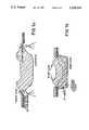
- FIGS. 4a and 4bshow a sectional view of a silicon wafer comprising a completely or partially buried localized oxidation in accordance with the subject of the invention
- FIG. 5ashows a dimensioned view of a silicon substrate S subjected to the process forming the subject of the present invention and corresponding to stage d) of FIG. 2;.
- FIG. 5bshows in section, in the same section plane as that of FIG. 5a, a dimensioned view of an integrated circuit forming the subject of the invention, comprising a buried oxide region produced by the process of the invention.
- the process forming the subject of the present inventionconsists successively in performing, on the free area of the silicon substrate, marked S, a sealing of this area by growing a layer of silicon nitride forming at least one surface layer.
- the layers cp1, cp2 and cp3are intended to produce the sealing of the free area of the silicon substrate S, this free area forming a horizontal interface.
- the first surface layer cp1is formed by a first nitriding by controlled growth, especially with regard to temperature and in the presence of ammonia, of a layer of silicon nitride on the free area of the substrate S, this layer obtained by diffusion of nitrogenous species originating from a reactive atmosphere into the surface layers of silicon being a thin layer whose thickness does not exceed 5 nm.
- the silicon substrate Sis placed for this purpose in an oven which optionally makes it possible to create an ammonia plasma and is subjected to the conventional treatment operations using an oven of this type, which will not be described in detail, since these operations respond to operations of a conventional type.
- Layer cp2is advantageously a layer of pedestal material such as, for example, silicon oxide SiO 2 or of polycrystalline silicon, it being possible for this layer to be deposited chemically in a vapor phase, optionally, for example, plasma-assisted, such a layer being deposited over a thickness of 10 to 25 nm.
- pedestal materialsuch as, for example, silicon oxide SiO 2 or of polycrystalline silicon
- the surface layer cp3is a silicon nitride layer deposited as a thick layer by a chemical process in a vapor phase, for example over a thickness of 20 nm to 100 nm.
- the layers cp1, cp2 and cp3form a particularly effective seal enabling the process according to the invention to continue to be applied.
- This latter processnext consists, as shown particularly at point b) of FIG. 2, in performing, following an appropriate masking stage, an etching marked G1 into the silicon substrate S and into the silicon nitride layer obtained by first nitriding in particular, in order to form a trench T intended to receive the buried localized oxidation.
- the etching G1is symbolized by arrows. It will be understood, of course, that, prior to the actual etching process, a process of masking by means of a resin has been suitably performed in order to represent, on the free area of the substrate S and, in particular, on the layers cp1, cp2 and cp3, forming the sealing, the two-dimensional shape of the trench T in which the buried oxide layer will be developed during the subsequent application of the process.
- the etching G1is performed by an anisotropic process using an adapted reactive ion etching to a depth of the order of a few hundred nm, counting from the substrate S/layer cp1 interface, for example.
- the process forming the subject of the present inventionconsists, after removal of the resin forming the etching mask, in performing, as shown at point c) of this same FIG. 2, a second nitriding on the free area of the trench T, to produce a sealing, marked sc, by growing a silicon nitride layer on the walls of the trench T.
- This second nitridingcan be advantageously performed by a treatment of the substrate S comprising the trench T under conditions which are similar to those needed to apply the first nitriding.
- the thickness of the silicon nitride layer producing the sealing scis of the order of 5 nm.
- the process forming the subject of the present inventioncan then consist, as shown at point d) of FIG. 2, in performing an etching marked G2 on the bottom wall of the trench T, or at least a part of the surface of this bottom wall, of the silicon nitride layer obtained by the second nitriding described above, in order to uncover the of the material silicon substrate.
- etching G2is also symbolized by vertical arrows in the same way as etching G1, it being advantageously possible for both these etchings to be carried out by means of adapted reactive ion etching processes generating an anisotropic etching of the silicon substrate.
- etching of the bottom wall of the trench and, in particular, of the sealing sc on this wallwill be described later in the description.
- the process forming the subject of the present inventionfinally consists in performing, as shown at point 2 of this same figure, a localized oxidation of the material, that is to say of the silicon laid bare at the bottom of trench T, to perform the buried oxidation--marked OE--of the substrate in the trench T.
- the substrateas obtained above at the end of the stage of the process as shown at point d) of FIG. 2, is then placed in an oven in a moist atmosphere, the temperature of which is, for example, between 900° C. and 1100° C.
- the substrate obtained after growth of the buried oxide layer OEhas been shown, the surface layers cp1, cp2 and cp3 having been removed, for example by selective etching.
- the depth of the trench T and the thickness of the localized oxide OEdetermines, in fact, the difference in alignment between the free area of the buried oxide OE and that of the silicon substrate S.
- the free area of the buried silicon oxide layer OEis substantially planar and parallel to that of the silicon substrate S after the layers cp1, cp2 and cp3 have been removed.
- the etching G1 which allows the trench T to be producedis carried out by an anisotropic etching process so that the trench T has substantially vertical side walls which are at right angles to the bottom wall of the trench.
- the process forming the subject of the present inventionmay additionally consist in depositing, as shown at c'), a thick layer CE of silicon oxide, shown using broken lines, covering the layer cp3 and the walls and bottoms of the trench, before the stage d) consisting in performing an at least partial etching of the silicon nitride layer obtained by second nitriding.
- a partial etching, marked G'1, of the thick silicon oxide layer CEis then performed to uncover part of the silicon nitride layer obtained on the bottom wall of the trench T by applying the second nitriding at the preceding stage c) of application of the process according to the invention.
- the partial etching G'1is preferably performed by anisotropic etching, symbolized by vertical arrows, and has the effect of maintaining, in the vicinity of the side walls of the trench T, a bead of oxide B protecting the silicon nitride layer obtained by the second nitriding.
- the result of the etching G'1is shown in c'') of FIG. 2.
- this protective bead Bensures the protection, during the etching G2, of the seal sc, on the one hand, on the vertical walls of the trench T and, on the other hand, on at least a part of the bottom wall of this same sealing layer sc.
- the process of etching of the trench as shown at point b) of FIG. 3is carried out by a semiisotropic etching so as to form a trench T' which has side walls which are substantially oblique relative to the bottom wall of the trench.
- the semiisotropic etching G1 at point b) of FIG. 3has been shown symbolically by vertical arrows extended by arrows forming a circular arc.
- the etching of the silicon substrate in the form of semiisotropic etchingis performed by means of a liquid chemical etching process or an adapted reactive ion etching process.
- the surface layer(s) cp1, cp2 and cp3form an overhang in relation to the oblique side walls of the trench T', this overhang having the effect of protecting from the etching the parts of the silicon nitride layer forming the sealing sc--a layer obtained by second nitriding--which are situated on the abovementioned oblique side walls and under this overhang.
- the etching G2is performed by an anisotropic etching so as to etch substantially solely the bottom wall of the trench T' in order to remove the sealing sc on this bottom wall.
- the substrateis then subjected, at point e) of FIG. 3, to a localized oxidation of the material to produce the buried oxidation, this oxidation being performed by thermal oxidation in a moist atmosphere.
- FIGS. 4a and 4bshow, furthermore, a silicon wafer S comprising at least one buried silicon oxide layer OE before removal of the layers cp1, cp2 and cp3.
- this oxide layercomprises a free area, planar and parallel to the free area of the substrate. It can be seen that the free area of the oxide may be situated above or below the free area of silicon, depending on the depth p of the trench produced and depending on the thickness of the buried oxide OE produced.
- FIG. 4ashows the case where ep is twice p and FIG. 4b the case where ep is equal to four times p.
- FIGS. 5a and 5bA more detailed description of an integrated circuit in accordance with the subject of the invention and exhibiting a buried oxide region produced by the process forming the subject of the invention will be given in conjunction with FIGS. 5a and 5b.
- FIG. 5ashows a dimensioned view of a silicon substrate S subjected to the process forming the subject of the invention and corresponding to stage d) of FIG. 2, that is after the etching stage G2.
- the trench T defined by the planes p1 and p2, which are transverse to the free area S1 of the silicon substrate Scomprises a central region C between the planes p'1 and p'2 defined by the silicon oxide beads B.
- p1p21.6 ⁇ m
- epg0.05 to 0.5 ⁇ m
- FIG. 5bshows a view in section in the same section plane as that of FIG. 5a, a dimensioned view of an integrated circuit forming the subject of the invention, comprising a buried oxide region produced by the process of the invention.
- the substrate Scomprises at least one buried oxide region OE in the trench T, which is defined by planes p1 and p2, transverse to the free area S1 of the substrate.
- the buried oxide region 0Ehas a uniform thickness epo over the central region C between an upper surface Ss and a lower surface Si which are planar and parallel to the free area S1 of the silicon substrate S. It will be noted that the central part C corresponds to the bottom area of the trench where the second nitride layer has been etched.
- the buried oxide region OEhas, in the side regions 11, 12 included between the central region C and the planes p1, p2 defining the trench T, that is between the planes p1, p'1 and p2, p'2 respectively, a thickness e which varies monotonically between the value of the thickness of the oxide buried in the central region epo and a thickness value epg, the depth of etching of the trench T into the silicon substrate S.
- the buried oxide layer OE in the vicinity of the edge of the trench Tthat is to say in the abovementioned side regions L1, L2, is free from any bird's head.
- the planes p1 and p2, and consequently p'1 and p'2are substantially at right angles to the free area S1 of the silicon substrate S.
- the buried oxide region OE at the interface with the substrate S at the height of the planes p1, p2exhibits a thickness equal to epg, the depth of etching of the trench T and, correspondingly, in the vicinity to the left of the same plane p1 and in particular under the mask cp1, a thickness which is substantially zero in the absence of any entry of oxide between the mask and the free area of the substrate, and conversely with regard to the right and left vicinities of the plane p2.
- the buried oxide region(s) OEare also free from any bird's beak.
- the nitriding process performed by a controlled reactive growth of the corresponding nitride layer, to perform the sealing sc of the walls of the trench T or T'is such that the nitride layer growing from the silicon surfaces is sufficiently effective to prevent the oxidation of the corresponding silicon surfaces and sufficiently thin--thinner or equal to 5 nm--to prevent the creation of mechanical stresses in the underlying silicon.
- the nitriding of silicon by a growth methodsuch as plasma-assisted nitriding makes it possible to obtain highly saturated growth kinetics which permit easy control of the final nitride thickness between 2 and 6 nm to form the sealing layer sc. It is therefore also possible to adjust without any difficulty the nitride thickness required as a function of the desired final thickness of the buried oxide.
- the plasma-assisted nitriding processgives rise to an isotropic growth of the nitride layer whatever the geometry of the areas to be nitrided. It is therefore also possible to nitride in a uniform manner the silicon areas of the active regions and those corresponding to the trench walls.
- the natural oxide present at the surface of the walls which are subjected to the abovementioned nitriding processis removed as early as in the first stages of the nitriding.
- Such a propertyensures the reproducibility of the process forming the subject of the present invention, because the natural oxide can differ from one silicon wafer to the next.
- the sealing obtainedis of a very high quality, the thin nitride layer obtained by the first and second nitriding being perfectly adherent to the silicon and prevents the side oxidation both under the sealing layer sc and under the thin nitride layer indicated by cp1 previously in the description, between the pedestal oxide cp2 and the free area of the silicon substrate.
- the oxidation of the wall of the trenches T or T'is prevented, thus limiting the production of excess oxide and therefore preventing the formation of the bird's head.
Landscapes
- Engineering & Computer Science (AREA)
- Physics & Mathematics (AREA)
- Condensed Matter Physics & Semiconductors (AREA)
- General Physics & Mathematics (AREA)
- Manufacturing & Machinery (AREA)
- Computer Hardware Design (AREA)
- Microelectronics & Electronic Packaging (AREA)
- Power Engineering (AREA)
- Element Separation (AREA)
- Local Oxidation Of Silicon (AREA)
Abstract
Description
Claims (8)
Applications Claiming Priority (2)
| Application Number | Priority Date | Filing Date | Title |
|---|---|---|---|
| FR9101381 | 1991-02-07 | ||
| FR9101381AFR2672731A1 (en) | 1991-02-07 | 1991-02-07 | PROCESS FOR BURIED LOCALIZED OXIDATION OF A SILICON SUBSTRATE AND CORRESPONDING INTEGRATED CIRCUIT |
Publications (1)
| Publication Number | Publication Date |
|---|---|
| US5229318Atrue US5229318A (en) | 1993-07-20 |
Family
ID=9409445
Family Applications (1)
| Application Number | Title | Priority Date | Filing Date |
|---|---|---|---|
| US07/832,078Expired - LifetimeUS5229318A (en) | 1991-02-07 | 1992-02-06 | Process for buried localized oxidation of a silicon substrate and corresponding integrated circuit |
Country Status (4)
| Country | Link |
|---|---|
| US (1) | US5229318A (en) |
| EP (1) | EP0498717A1 (en) |
| JP (1) | JPH0555367A (en) |
| FR (1) | FR2672731A1 (en) |
Cited By (20)
| Publication number | Priority date | Publication date | Assignee | Title |
|---|---|---|---|---|
| US5372950A (en)* | 1991-05-18 | 1994-12-13 | Samsung Electronics Co., Ltd. | Method for forming isolation regions in a semiconductor memory device |
| US5399520A (en)* | 1993-03-31 | 1995-03-21 | Hyundai Electronics Industries Co., Ltd. | Method for the formation of field oxide film in semiconductor device |
| US5470783A (en)* | 1994-06-06 | 1995-11-28 | At&T Ipm Corp. | Method for integrated circuit device isolation |
| US5494857A (en)* | 1993-07-28 | 1996-02-27 | Digital Equipment Corporation | Chemical mechanical planarization of shallow trenches in semiconductor substrates |
| US5510290A (en)* | 1994-04-01 | 1996-04-23 | Hyundai Electronics Industries Co., Ltd. | Method for forming a field oxide layer in a semiconductor device which prevents bird beak by nitradation of pad oxide |
| DE19525072A1 (en)* | 1995-07-10 | 1997-01-16 | Siemens Ag | Integrated circuit arrangement with at least two components isolated from one another and method for their production |
| US5672538A (en)* | 1995-12-04 | 1997-09-30 | Taiwan Semiconductor Manufacturing Company, Ltd | Modified locus isolation process in which surface topology of the locos oxide is smoothed |
| US5721174A (en)* | 1997-02-03 | 1998-02-24 | Chartered Semiconductor Manufacturing Pte Ltd | Narrow deep trench isolation process with trench filling by oxidation |
| US5726093A (en)* | 1995-12-06 | 1998-03-10 | Taiwan Semiconductor Manufacturing Company Ltd. | Two-step planer field oxidation method |
| US5789305A (en)* | 1997-01-27 | 1998-08-04 | Chartered Semiconductor Manufacturing Ltd. | Locos with bird's beak suppression by a nitrogen implantation |
| US5940718A (en)* | 1998-07-20 | 1999-08-17 | Advanced Micro Devices | Nitridation assisted polysilicon sidewall protection in self-aligned shallow trench isolation |
| US6033997A (en)* | 1997-12-29 | 2000-03-07 | Siemens Aktiengesellschaft | Reduction of black silicon in semiconductor fabrication |
| US6080665A (en)* | 1997-04-11 | 2000-06-27 | Applied Materials, Inc. | Integrated nitrogen-treated titanium layer to prevent interaction of titanium and aluminum |
| US6613651B1 (en)* | 2000-09-05 | 2003-09-02 | Lsi Logic Corporation | Integrated circuit isolation system |
| US6703280B2 (en)* | 1999-10-25 | 2004-03-09 | Samsung Electronics Co., Ltd. | SOI semiconductor integrated circuit for eliminating floating body effects in SOI MOSFETs and method of fabricating the same |
| US20050136595A1 (en)* | 2003-12-22 | 2005-06-23 | Tomokazu Horie | Method for manufacturing semiconductor device |
| US20060057755A1 (en)* | 2004-09-14 | 2006-03-16 | Heribert Weber | Micromechanical component and suitable method for its manufacture |
| US8772902B2 (en) | 2012-04-19 | 2014-07-08 | International Business Machines Corporation | Fabrication of a localized thick box with planar oxide/SOI interface on bulk silicon substrate for silicon photonics integration |
| US9105686B2 (en) | 2012-11-02 | 2015-08-11 | International Business Machines Corporation | Fabrication of localized SOI on localized thick box using selective epitaxy on bulk semiconductor substrates for photonics device integration |
| US10410798B2 (en)* | 2014-10-17 | 2019-09-10 | Teknologian Tutkimuskeskus Vtt Oy | Blank suitable for use as a body of a supercapacitor, a supercapacitor, and a method of manufacturing a porous silicon volume |
Families Citing this family (3)
| Publication number | Priority date | Publication date | Assignee | Title |
|---|---|---|---|---|
| KR970003731B1 (en)* | 1993-10-14 | 1997-03-21 | 엘지반도체 주식회사 | Device isolation film manufacturing method of semiconductor device |
| US5661073A (en)* | 1995-08-11 | 1997-08-26 | Micron Technology, Inc. | Method for forming field oxide having uniform thickness |
| CZ293360B6 (en)* | 1995-10-26 | 2004-04-14 | Sanofi-Synthelabo | Medicament intended for the treatment of amyotrophic lateral sclerosis |
Citations (8)
| Publication number | Priority date | Publication date | Assignee | Title |
|---|---|---|---|---|
| US3958040A (en)* | 1973-09-07 | 1976-05-18 | U.S. Philips Corporation | Semiconductor device manufacture |
| EP0052948A1 (en)* | 1980-11-24 | 1982-06-02 | Motorola, Inc. | Oxide isolation process |
| JPS58169935A (en)* | 1982-03-30 | 1983-10-06 | Matsushita Electronics Corp | Manufacture of semiconductor device |
| DE3418638A1 (en)* | 1983-05-20 | 1984-11-22 | Kabushiki Kaisha Toshiba, Kawasaki, Kanagawa | Process for fabricating a semiconductor device |
| US4533429A (en)* | 1982-10-08 | 1985-08-06 | U.S. Philips Corporation | Method of manufacturing a semiconductor device |
| US4563227A (en)* | 1981-12-08 | 1986-01-07 | Matsushita Electric Industrial Co., Ltd. | Method for manufacturing a semiconductor device |
| WO1988010510A1 (en)* | 1987-06-15 | 1988-12-29 | Ncr Corporation | Semiconductor field oxide formation process |
| US4986879A (en)* | 1987-06-15 | 1991-01-22 | Ncr Corporation | Structure and process for forming semiconductor field oxide using a sealing sidewall of consumable nitride |
Family Cites Families (1)
| Publication number | Priority date | Publication date | Assignee | Title |
|---|---|---|---|---|
| FR2648956A1 (en)* | 1989-06-23 | 1990-12-28 | Commissariat Energie Atomique | PROCESS FOR PRODUCING FIELD OXIDE OF AN INTEGRATED CIRCUIT ON SILICON |
- 1991
- 1991-02-07FRFR9101381Apatent/FR2672731A1/enactiveGranted
- 1992
- 1992-02-05EPEP92400287Apatent/EP0498717A1/ennot_activeWithdrawn
- 1992-02-05JPJP4020246Apatent/JPH0555367A/ennot_activeWithdrawn
- 1992-02-06USUS07/832,078patent/US5229318A/ennot_activeExpired - Lifetime
Patent Citations (9)
| Publication number | Priority date | Publication date | Assignee | Title |
|---|---|---|---|---|
| US3958040A (en)* | 1973-09-07 | 1976-05-18 | U.S. Philips Corporation | Semiconductor device manufacture |
| GB1437112A (en)* | 1973-09-07 | 1976-05-26 | Mullard Ltd | Semiconductor device manufacture |
| EP0052948A1 (en)* | 1980-11-24 | 1982-06-02 | Motorola, Inc. | Oxide isolation process |
| US4563227A (en)* | 1981-12-08 | 1986-01-07 | Matsushita Electric Industrial Co., Ltd. | Method for manufacturing a semiconductor device |
| JPS58169935A (en)* | 1982-03-30 | 1983-10-06 | Matsushita Electronics Corp | Manufacture of semiconductor device |
| US4533429A (en)* | 1982-10-08 | 1985-08-06 | U.S. Philips Corporation | Method of manufacturing a semiconductor device |
| DE3418638A1 (en)* | 1983-05-20 | 1984-11-22 | Kabushiki Kaisha Toshiba, Kawasaki, Kanagawa | Process for fabricating a semiconductor device |
| WO1988010510A1 (en)* | 1987-06-15 | 1988-12-29 | Ncr Corporation | Semiconductor field oxide formation process |
| US4986879A (en)* | 1987-06-15 | 1991-01-22 | Ncr Corporation | Structure and process for forming semiconductor field oxide using a sealing sidewall of consumable nitride |
Non-Patent Citations (12)
| Title |
|---|
| Dave Bursky, "CMOS Process Breaks Bird's Beak Barrier", Electronic Design, vol. 37, No. 24, Nov. 1989. |
| Dave Bursky, CMOS Process Breaks Bird s Beak Barrier , Electronic Design, vol. 37, No. 24, Nov. 1989.* |
| K. Tsukamoto et al., "Peripheral Capacitor Cell with Fully Recessed Isolation for Megabit DRAM", Japanese Journal of Applied Physics, Supplements, pp. 295-298, Aug. 1986. |
| K. Tsukamoto et al., Peripheral Capacitor Cell with Fully Recessed Isolation for Megabit DRAM , Japanese Journal of Applied Physics, Supplements, pp. 295 298, Aug. 1986.* |
| Kuang Yi Chiu et al., "A Bird's Beak Free Local Oxidation Technology Feasible for VLSI Circuit's Fabrication", IEEE Transactions on Electron Devices, vol. ED-29, No. 4, pp. 536-540, Apr. 1982. |
| Kuang Yi Chiu et al., A Bird s Beak Free Local Oxidation Technology Feasible for VLSI Circuit s Fabrication , IEEE Transactions on Electron Devices, vol. ED 29, No. 4, pp. 536 540, Apr. 1982.* |
| Russel Martin, "Spacer for Improved Local Oxidation Profile", Xerox Disclosure Journal, vol. 12, No. 5, pp. 251-253, Sep. 1987. |
| Russel Martin, Spacer for Improved Local Oxidation Profile , Xerox Disclosure Journal, vol. 12, No. 5, pp. 251 253, Sep. 1987.* |
| S. S. Lee et al., "A Novel CMOS Isolation Technology Using a Consumable Nitride Seal During Field Oxidation", Extended Abstracts, Spring Meeting Montreal, vol. 90-1, pp. 616-617, May 1990. |
| S. S. Lee et al., A Novel CMOS Isolation Technology Using a Consumable Nitride Seal During Field Oxidation , Extended Abstracts, Spring Meeting Montreal, vol. 90 1, pp. 616 617, May 1990.* |
| V. K. Dwivedi, "A Bird's-Beak-free Sealed-Interface Local Oxidation Technology for Submicron Ultra-Large-Scale Integrated Circuits", Journal of Electrochemical Society, vol. 137, No. 8, pp. 2586-2588, Aug. 1990. |
| V. K. Dwivedi, A Bird s Beak free Sealed Interface Local Oxidation Technology for Submicron Ultra Large Scale Integrated Circuits , Journal of Electrochemical Society, vol. 137, No. 8, pp. 2586 2588, Aug. 1990.* |
Cited By (25)
| Publication number | Priority date | Publication date | Assignee | Title |
|---|---|---|---|---|
| US5372950A (en)* | 1991-05-18 | 1994-12-13 | Samsung Electronics Co., Ltd. | Method for forming isolation regions in a semiconductor memory device |
| US5399520A (en)* | 1993-03-31 | 1995-03-21 | Hyundai Electronics Industries Co., Ltd. | Method for the formation of field oxide film in semiconductor device |
| US5494857A (en)* | 1993-07-28 | 1996-02-27 | Digital Equipment Corporation | Chemical mechanical planarization of shallow trenches in semiconductor substrates |
| US5510290A (en)* | 1994-04-01 | 1996-04-23 | Hyundai Electronics Industries Co., Ltd. | Method for forming a field oxide layer in a semiconductor device which prevents bird beak by nitradation of pad oxide |
| DE19512148C2 (en)* | 1994-04-01 | 2002-06-20 | Hyundai Electronics Ind | Method for producing a field oxide layer in a semiconductor device |
| US5470783A (en)* | 1994-06-06 | 1995-11-28 | At&T Ipm Corp. | Method for integrated circuit device isolation |
| DE19525072C2 (en)* | 1995-07-10 | 2002-06-27 | Infineon Technologies Ag | Integrated circuit arrangement in which a first component is arranged on a main surface of a semiconductor substrate and a second component on the trench bottom, and method for the production thereof |
| DE19525072A1 (en)* | 1995-07-10 | 1997-01-16 | Siemens Ag | Integrated circuit arrangement with at least two components isolated from one another and method for their production |
| US5990536A (en)* | 1995-07-10 | 1999-11-23 | Siemens Aktiengesellschaft | Integrated circuit arrangement having at least two mutually insulated components, and method for its production |
| US5672538A (en)* | 1995-12-04 | 1997-09-30 | Taiwan Semiconductor Manufacturing Company, Ltd | Modified locus isolation process in which surface topology of the locos oxide is smoothed |
| US5726093A (en)* | 1995-12-06 | 1998-03-10 | Taiwan Semiconductor Manufacturing Company Ltd. | Two-step planer field oxidation method |
| US5789305A (en)* | 1997-01-27 | 1998-08-04 | Chartered Semiconductor Manufacturing Ltd. | Locos with bird's beak suppression by a nitrogen implantation |
| US5721174A (en)* | 1997-02-03 | 1998-02-24 | Chartered Semiconductor Manufacturing Pte Ltd | Narrow deep trench isolation process with trench filling by oxidation |
| US6080665A (en)* | 1997-04-11 | 2000-06-27 | Applied Materials, Inc. | Integrated nitrogen-treated titanium layer to prevent interaction of titanium and aluminum |
| US6033997A (en)* | 1997-12-29 | 2000-03-07 | Siemens Aktiengesellschaft | Reduction of black silicon in semiconductor fabrication |
| US5940718A (en)* | 1998-07-20 | 1999-08-17 | Advanced Micro Devices | Nitridation assisted polysilicon sidewall protection in self-aligned shallow trench isolation |
| US6703280B2 (en)* | 1999-10-25 | 2004-03-09 | Samsung Electronics Co., Ltd. | SOI semiconductor integrated circuit for eliminating floating body effects in SOI MOSFETs and method of fabricating the same |
| US6613651B1 (en)* | 2000-09-05 | 2003-09-02 | Lsi Logic Corporation | Integrated circuit isolation system |
| US20050136595A1 (en)* | 2003-12-22 | 2005-06-23 | Tomokazu Horie | Method for manufacturing semiconductor device |
| US20060057755A1 (en)* | 2004-09-14 | 2006-03-16 | Heribert Weber | Micromechanical component and suitable method for its manufacture |
| US7435691B2 (en)* | 2004-09-14 | 2008-10-14 | Robert Bosch Gmbh | Micromechanical component and suitable method for its manufacture |
| US8772902B2 (en) | 2012-04-19 | 2014-07-08 | International Business Machines Corporation | Fabrication of a localized thick box with planar oxide/SOI interface on bulk silicon substrate for silicon photonics integration |
| US9105686B2 (en) | 2012-11-02 | 2015-08-11 | International Business Machines Corporation | Fabrication of localized SOI on localized thick box using selective epitaxy on bulk semiconductor substrates for photonics device integration |
| US9236287B2 (en) | 2012-11-02 | 2016-01-12 | GLOBALFOUNDIES Inc. | Fabrication of localized SOI on localized thick box lateral epitaxial realignment of deposited non-crystalline film on bulk semiconductor substrates for photonics device integration |
| US10410798B2 (en)* | 2014-10-17 | 2019-09-10 | Teknologian Tutkimuskeskus Vtt Oy | Blank suitable for use as a body of a supercapacitor, a supercapacitor, and a method of manufacturing a porous silicon volume |
Also Published As
| Publication number | Publication date |
|---|---|
| FR2672731B1 (en) | 1997-03-07 |
| JPH0555367A (en) | 1993-03-05 |
| EP0498717A1 (en) | 1992-08-12 |
| FR2672731A1 (en) | 1992-08-14 |
Similar Documents
| Publication | Publication Date | Title |
|---|---|---|
| US5229318A (en) | Process for buried localized oxidation of a silicon substrate and corresponding integrated circuit | |
| US6326282B1 (en) | Method of forming trench isolation in a semiconductor device and structure formed thereby | |
| US6747333B1 (en) | Method and apparatus for STI using passivation material for trench bottom liner | |
| JPS6340337A (en) | Method of isolating integrated circuit | |
| US5604149A (en) | Method of and device for isolating active areas of a semiconducor substrate by quasi-plane shallow trenches | |
| US5264395A (en) | Thin SOI layer for fully depleted field effect transistors | |
| JPH0580148B2 (en) | ||
| JPH01276641A (en) | Manufacture of semiconductor device | |
| JPH0526337B2 (en) | ||
| KR100428804B1 (en) | Method of forming a layer in an integrated circuit device process, a method for fabricating a trench isolaton using the same and a trench isolation structure | |
| KR100270464B1 (en) | Method of forming recessed oxide isolation | |
| US6368976B1 (en) | Method for manufacturing a semiconductor device having film thickness difference between a control gate and a floating gate | |
| US6521510B1 (en) | Method for shallow trench isolation with removal of strained island edges | |
| US5641704A (en) | Method of isolating active areas of a semiconductor substrate by shallow trenches and narrow trenches | |
| US4960727A (en) | Method for forming a dielectric filled trench | |
| US5894059A (en) | Dislocation free local oxidation of silicon with suppression of narrow space field oxide thinning effect | |
| US5736451A (en) | Method of forming planar isolation in integrated circuits | |
| KR100286127B1 (en) | How to Form Trench Isolation in Semiconductor Devices | |
| USRE34400E (en) | Method for fabricating isolation region in semiconductor devices | |
| EP0612438A1 (en) | Process for fabricating insulation-filled deep trenches in semiconductor substrates | |
| US6284625B1 (en) | Method of forming a shallow groove isolation structure | |
| US6444539B1 (en) | Method for producing a shallow trench isolation filled with thermal oxide | |
| JPS6358370B2 (en) | ||
| JP3102197B2 (en) | Wafer dielectric isolation method | |
| JPS5992547A (en) | Isolation method |
Legal Events
| Date | Code | Title | Description |
|---|---|---|---|
| AS | Assignment | Owner name:FRANCE TELECOM, FRANCE Free format text:ASSIGNMENT OF ASSIGNORS INTEREST.;ASSIGNORS:STRABONI, ALAIN;BARLA, KATHY;VUILLERMOZ, BERNARD;REEL/FRAME:006006/0274 Effective date:19920115 | |
| FEPP | Fee payment procedure | Free format text:PAYOR NUMBER ASSIGNED (ORIGINAL EVENT CODE: ASPN); ENTITY STATUS OF PATENT OWNER: LARGE ENTITY | |
| STCF | Information on status: patent grant | Free format text:PATENTED CASE | |
| FPAY | Fee payment | Year of fee payment:4 | |
| FEPP | Fee payment procedure | Free format text:PAYER NUMBER DE-ASSIGNED (ORIGINAL EVENT CODE: RMPN); ENTITY STATUS OF PATENT OWNER: LARGE ENTITY Free format text:PAYOR NUMBER ASSIGNED (ORIGINAL EVENT CODE: ASPN); ENTITY STATUS OF PATENT OWNER: LARGE ENTITY | |
| FPAY | Fee payment | Year of fee payment:8 | |
| REMI | Maintenance fee reminder mailed | ||
| FPAY | Fee payment | Year of fee payment:12 | |
| SULP | Surcharge for late payment | Year of fee payment:11 | |
| AS | Assignment | Owner name:FAHRENHEIT THERMOSCOPE, LLC, NEVADA Free format text:ASSIGNMENT OF ASSIGNORS INTEREST;ASSIGNOR:FRANCE TELECOM INC.;REEL/FRAME:018022/0941 Effective date:20041203 | |
| FEPP | Fee payment procedure | Free format text:PAYOR NUMBER ASSIGNED (ORIGINAL EVENT CODE: ASPN); ENTITY STATUS OF PATENT OWNER: LARGE ENTITY Free format text:PAYER NUMBER DE-ASSIGNED (ORIGINAL EVENT CODE: RMPN); ENTITY STATUS OF PATENT OWNER: LARGE ENTITY | |
| AS | Assignment | Owner name:FAHRENHEIT THERMOSCOPE LLC, NEVADA Free format text:CORRECTIVE ASSIGNMENT TO CORRECT THE ASSIGNOR NAME PREVIOUSLY RECORDED ON REEL 018022 FRAME 0941. ASSIGNOR(S) HEREBY CONFIRMS THE ASSIGNOR NAME IS FRANCE TELECOM S.A., NOT FRANCE TELECOM INC;ASSIGNOR:FRANCE TELECOM S.A.;REEL/FRAME:024723/0327 Effective date:20041203 |