US5228966A - Gilding apparatus for semiconductor substrate - Google Patents
Gilding apparatus for semiconductor substrateDownload PDFInfo
- Publication number
- US5228966A US5228966AUS07/823,158US82315892AUS5228966AUS 5228966 AUS5228966 AUS 5228966AUS 82315892 AUS82315892 AUS 82315892AUS 5228966 AUS5228966 AUS 5228966A
- Authority
- US
- United States
- Prior art keywords
- semiconductor substrate
- cathode electrode
- tank
- cup
- vacuum
- Prior art date
- Legal status (The legal status is an assumption and is not a legal conclusion. Google has not performed a legal analysis and makes no representation as to the accuracy of the status listed.)
- Expired - Lifetime
Links
- 239000000758substrateSubstances0.000titleclaimsabstractdescription66
- 239000004065semiconductorSubstances0.000titleclaimsabstractdescription58
- 230000007246mechanismEffects0.000claimsabstractdescription16
- 239000007788liquidSubstances0.000claimsdescription13
- 230000003247decreasing effectEffects0.000description4
- 238000009826distributionMethods0.000description3
Images


Classifications
- H—ELECTRICITY
- H01—ELECTRIC ELEMENTS
- H01L—SEMICONDUCTOR DEVICES NOT COVERED BY CLASS H10
- H01L21/00—Processes or apparatus adapted for the manufacture or treatment of semiconductor or solid state devices or of parts thereof
- H01L21/67—Apparatus specially adapted for handling semiconductor or electric solid state devices during manufacture or treatment thereof; Apparatus specially adapted for handling wafers during manufacture or treatment of semiconductor or electric solid state devices or components ; Apparatus not specifically provided for elsewhere
- H01L21/67005—Apparatus not specifically provided for elsewhere
- H01L21/67011—Apparatus for manufacture or treatment
- H01L21/6715—Apparatus for applying a liquid, a resin, an ink or the like
Definitions
- the present inventionrelates to a structure of a gilding apparatus for performing a gilding treatment by jetting a gilt liquid in a metalizing step of a semiconductor substrate.
- a cup-like tank 2has a gilt liquid supply port 3, an anode electrode 5, and a semiconductor substrate support member 18, and the cup-like tank 2 is integrated with an outer tank 1.
- a gilt liquid 11 having a temperature controlled by a pump 9is supplied from the gilt liquid supply port 3 to the cup-like tank 2 through a filter 8, and the gilt liquid 11 is jetted through the anode electrode 5.
- a semiconductor substrate 6 having a lower surface to be treatedis supported by the semiconductor substrate support member 18 to be close to an upper opening 2a of the cup-like tank 2.
- a head member 10 vertically moved by a lifting mechanism member 17 through a base plate 16is moved downward to be set and brought into contact with the semiconductor substrate 6, and a cross-shaped and leaf-spring-like cathode electrode 4e (shown in FIG. 4B) arranged on the heat member 10 is brought into contact with the semiconductor substrate 6 and is urged against the lower surface of the semiconductor substrate 6.
- a potential differenceis applied between the anode electrode 5 and the cathode electrode 4e, thereby performing a gilding treatment.
- a pin-like cathode electrode 4fis brought into contact with and urged against a semiconductor substrate 6 by elastic forces of springs, and a potential difference is applied between the anode electrode 5 and the cathode electrode 4f, thereby performing a gilding treatment.
- the cathode electrode using an elastic force of a springsince the cathode electrode using an elastic force of a spring is used as the contact portion on the cathode side, the elastic force does not easily have uniformity and resistances of the contact portions between a plurality of spring-like cathode electrodes and the semiconductor substrate are different from each other.
- a gilding treatmentis performed in this state, a gilt thickness is increased near a position having a low contact resistance, and a gilt thickness is decreased near a position having a high contact resistance, thereby varying the gilt thickness on the plated surface of the semiconductor substrate.
- a surface with which the cathode electrodes are in contact and which is to be platedtends to be plated thick, and the gilt thickness is disadvantageously varied.
- a gilding apparatus for a semiconductor substratecomprising a cup-like tank for jetting a gilt liquid from a gilt liquid supply port formed in a bottom portion of the cup-like tank through an anode electrode, a substrate support member on which a semiconductor substrate having a lower surface to be treated is mounted to be close to an upper opening of the cup-like tank, a cathode electrode having the same area as that of the semiconductor substrate and brought into contact with the semiconductor substrate mounted on the substrate support member from an upper direction, and an adjusting mechanism for keeping the cathode electrode and the semiconductor mounted on the substrate support member to be relatively horizontal.
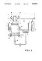
- FIG. 1is a cross-sectional view showing a gilding apparatus according to the first embodiment of the present invention
- FIG. 2is a view showing an overall arrangement of the first embodiment of the present invention
- FIG. 3Ais a sectional side view showing a gilding apparatus according to the second embodiment of the present invention.
- FIG. 3Bis a view showing the bottom surface of a chuck member in FIG. 3A;
- FIG. 4Ais a sectional side view showing a conventional gilding apparatus
- FIG. 4Bis a front view showing a cathode electrode in FIG. 4A;
- FIG. 5is a view showing an overall arrangement of the conventional gilding apparatus
- FIG. 6is a sectional side view showing the conventional gilding apparatus
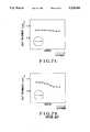
- FIG. 7Ais a graph showing a distribution of a gilt thickness on a semiconductor substrate when a gilding treatment is performed by a gilding apparatus according to the present invention.
- FIG. 7Bis a graph showing a distribution of a gilt thickness when a gilding treatment is performed by a conventional gilding apparatus.
- FIGS. 1 and 2are views showing the first embodiment of the present invention.
- an outer tank 1is filled with a gilt liquid 11, and the gilt liquid 11 is heated by a heater 7 to have a predetermined temperature.
- the gilt liquid 11 having a controlled temperatureis supplied from a gilt liquid supply port 3 to a cup-like tank 2 by a pump 9 and jetted through an anode electrode 5 arranged in the cup-like tank 2.
- a semiconductor substrate 6is supported by a semiconductor substrate support member 18 which is fixed to the cup-like tank 2 to be close to an upper opening 2a of the cup-like tank 2, and the semiconductor substrate 6 has a lower surface to be treated.
- a head member 10 having a cathode electrode 4is moved downward by a lifting member 17 to cause the cathode electrode 4 to be brought into contact with the rear surface of the semiconductor substrate 6, and a potential difference is applied between the anode electrode 5 and the cathode electrode 4.
- the cup-like tank 2 and the outer tank 1are independently arranged, and the outer tank 1 has a circular uprightportion 1a at the opening edge of a position at which the cup-like tank 2 is arranged.
- a circular skirt portion 2b having a diameter larger than that of the uprightportion 1ais formed on the outer periphery of the cup-like tank 2 to be suspended.
- An adjusting mechanism 13 for horizontally adjusting the overflow surface of the cup-like tank 2is arranged on the bottom portion of the cup-like tank 2.
- the cathode electrode 4is supported by the head member 10 which is supported by a bushing member 15 to be vertically moved, and the weight of the cathode electrode 4 itself including the head member 10 can act on the semiconductor substrate 6 such that the head member 10 is moved downward by the lifting member 17.
- the bushing member 15 for supporting the head member 10has an adjusting mechanism 14, and it keeps the cathode electrode 14 and the semiconductor substrate 6 supported on the cup-like tank 2 through the substrate support member 18 to be horizontal. Therefore, a load on the semiconductor substrate 6 can be uniformed.
- reference numeral 16denotes a base plate. As shown in FIG. 1, the cathode electrode 4 has the same area as that of one surface of the semiconductor substrate 6.
- the cathode electrode 4includes an elastic member 4b having a plurality of projections and made of rubber such as fluorine-contained rubber and a mesh-like cathode electrode 4a made of, e.g., a Pt mesh, and stretched on the lower surface of the elastic member 4b having the projections, such that the mesh-like cathode electrode 4a can be brought into uniform contact with the entire surface of the semiconductor substrate 6.
- the cathode electrode 4may have a structure having an elastic force acting on the entire surface of the semiconductor substrate 6 and may be formed by, e.g., conductive rubber.
- the adjusting mechanism 13keeps the semiconductor substrate 6 on the cup-like tank 2 to be horizontal, and the adjusting mechanism 14 keeps the cathode electrode 4 to be horizontal. Therefore, the cathode electrode 4 can be brought into contact with the semiconductor substrate 6 such that the cathode electrode 4 is brought into uniform contact with the entire surface of the semiconductor substrate 6 to cause a load to uniformly act on the substrate 6.
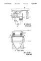
- FIG. 3Ais a sectional side view showing the second embodiment of the present invention
- FIG. 3Bis a bottom view showing a check member.
- a flat, conductive, vacuum-chucking cathode electrode 4chaving the same area as that of a semiconductor substrate 6 and cross-shaped, concentric vacuum-sucking grooves 4d for vacuum-chucking the semiconductor substrate 6 on the contact surface of the cathode electrode 4c are arranged.
- the head member 10is moved downward by a lifting mechanism member 17 on the semiconductor substrate 6, and the semiconductor substrate 6 is vacuum-chucked through tubes 19 arranged in the vacuum-chucking cathode electrode 4c.
- FIG. 1is a sectional side view showing the second embodiment of the present invention
- FIG. 3Bis a bottom view showing a check member.
- a flat, conductive, vacuum-chucking cathode electrode 4chaving the same area as that of a semiconductor substrate 6 and cross-shaped, concentric vacuum-sucking grooves 4d for vacuum-chucking the semiconductor substrate 6
- FIGS. 7A and 7Bare graphs showing gilt thickness distributions when a gilding treatment is performed.
- FIG. 7Bshows a case wherein a gilding treatment is performed by a conventional gilding apparatus. Referring to FIG. 7B, since a cathode electrode has variations in contact resistance, variations in gilt thickness are large.
- FIG. 7Ashows a case wherein a gilding treatment is performed by a gilding apparatus of the present invention. Referring to FIG. 7A, variations in gilt thickness are decreased.
- a gilding apparatushas a mechanism in which a cathode electrode having the same area as that of a semiconductor substrate can be brought into reliable contact with the almost entire surface of the semiconductor substrate, thereby decreasing variations in contact resistance on the contact surface between the semiconductor substrate and the cathode electrodes. Therefore, variations in gilt thickness on a surface to be gilt of the semiconductor substrate can be decreased, and a gilding treatment can be performed at a high accuracy.
Landscapes
- Engineering & Computer Science (AREA)
- Physics & Mathematics (AREA)
- Condensed Matter Physics & Semiconductors (AREA)
- General Physics & Mathematics (AREA)
- Manufacturing & Machinery (AREA)
- Computer Hardware Design (AREA)
- Microelectronics & Electronic Packaging (AREA)
- Power Engineering (AREA)
- Electroplating Methods And Accessories (AREA)
Abstract
Description
Claims (8)
Applications Claiming Priority (2)
| Application Number | Priority Date | Filing Date | Title |
|---|---|---|---|
| JP3-32113 | 1991-01-31 | ||
| JP3032113AJP2737416B2 (en) | 1991-01-31 | 1991-01-31 | Plating equipment |
Publications (1)
| Publication Number | Publication Date |
|---|---|
| US5228966Atrue US5228966A (en) | 1993-07-20 |
Family
ID=12349850
Family Applications (1)
| Application Number | Title | Priority Date | Filing Date |
|---|---|---|---|
| US07/823,158Expired - LifetimeUS5228966A (en) | 1991-01-31 | 1992-01-21 | Gilding apparatus for semiconductor substrate |
Country Status (2)
| Country | Link |
|---|---|
| US (1) | US5228966A (en) |
| JP (1) | JP2737416B2 (en) |
Cited By (36)
| Publication number | Priority date | Publication date | Assignee | Title |
|---|---|---|---|---|
| US5391285A (en)* | 1994-02-25 | 1995-02-21 | Motorola, Inc. | Adjustable plating cell for uniform bump plating of semiconductor wafers |
| US5417830A (en)* | 1992-12-02 | 1995-05-23 | Kabushiki Kaisha Toshiba | Injection plating apparatus |
| US5725742A (en)* | 1993-03-17 | 1998-03-10 | Daimler-Benz Ag | Device for electrolytic oxidation of silicon wafers |
| US5869139A (en)* | 1997-02-28 | 1999-02-09 | International Business Machines Corporation | Apparatus and method for plating pin grid array packaging modules |
| WO1999016936A1 (en)* | 1997-09-30 | 1999-04-08 | Semitool, Inc. | Electroplating system having auxiliary electrode exterior to main reactor chamber for contact cleaning operations |
| US6022465A (en)* | 1998-06-01 | 2000-02-08 | Cutek Research, Inc. | Apparatus and method utilizing an electrode adapter for customized contact placement on a wafer |
| US6093291A (en)* | 1997-09-02 | 2000-07-25 | Oki Electric Industry Co., Ltd. | Electroplating apparatus |
| US6099712A (en)* | 1997-09-30 | 2000-08-08 | Semitool, Inc. | Semiconductor plating bowl and method using anode shield |
| US6103096A (en)* | 1997-11-12 | 2000-08-15 | International Business Machines Corporation | Apparatus and method for the electrochemical etching of a wafer |
| US6106687A (en)* | 1998-04-28 | 2000-08-22 | International Business Machines Corporation | Process and diffusion baffle to modulate the cross sectional distribution of flow rate and deposition rate |
| US6113759A (en)* | 1998-12-18 | 2000-09-05 | International Business Machines Corporation | Anode design for semiconductor deposition having novel electrical contact assembly |
| US6251251B1 (en) | 1998-11-16 | 2001-06-26 | International Business Machines Corporation | Anode design for semiconductor deposition |
| US6261426B1 (en) | 1999-01-22 | 2001-07-17 | International Business Machines Corporation | Method and apparatus for enhancing the uniformity of electrodeposition or electroetching |
| US20020040679A1 (en)* | 1990-05-18 | 2002-04-11 | Reardon Timothy J. | Semiconductor processing apparatus |
| US20020046952A1 (en)* | 1997-09-30 | 2002-04-25 | Graham Lyndon W. | Electroplating system having auxiliary electrode exterior to main reactor chamber for contact cleaning operations |
| US20030053186A1 (en)* | 2001-09-19 | 2003-03-20 | Olympus Optical Co., Ltd. | Movable structure, and deflection mirror element, optical switch element and shape variable mirror including the movable structure |
| US20040007467A1 (en)* | 2002-05-29 | 2004-01-15 | Mchugh Paul R. | Method and apparatus for controlling vessel characteristics, including shape and thieving current for processing microfeature workpieces |
| US6741444B2 (en)* | 2001-07-23 | 2004-05-25 | Océ-Technologies B.V. | Apparatus for charging a substrate and an image forming apparatus comprising an apparatus of this kind |
| US20040173454A1 (en)* | 2001-10-16 | 2004-09-09 | Applied Materials, Inc. | Apparatus and method for electro chemical plating using backsid electrical contacte |
| US6916412B2 (en) | 1999-04-13 | 2005-07-12 | Semitool, Inc. | Adaptable electrochemical processing chamber |
| US20050178657A1 (en)* | 2003-10-09 | 2005-08-18 | Kirby Kyle K. | Systems and methods of plating via interconnects |
| US7020537B2 (en) | 1999-04-13 | 2006-03-28 | Semitool, Inc. | Tuning electrodes used in a reactor for electrochemically processing a microelectronic workpiece |
| US7090751B2 (en) | 2001-08-31 | 2006-08-15 | Semitool, Inc. | Apparatus and methods for electrochemical processing of microelectronic workpieces |
| US7115196B2 (en) | 1998-03-20 | 2006-10-03 | Semitool, Inc. | Apparatus and method for electrochemically depositing metal on a semiconductor workpiece |
| US20060254808A1 (en)* | 2004-01-12 | 2006-11-16 | Farnworth Warren M | Substrate precursor structures |
| US7147760B2 (en) | 1998-07-10 | 2006-12-12 | Semitool, Inc. | Electroplating apparatus with segmented anode array |
| US7160421B2 (en) | 1999-04-13 | 2007-01-09 | Semitool, Inc. | Turning electrodes used in a reactor for electrochemically processing a microelectronic workpiece |
| US20070023277A1 (en)* | 2003-01-21 | 2007-02-01 | Dainippon Screen Mfg. Co., Ltd. | Plating apparatus, plating cup and cathode ring |
| US7189318B2 (en) | 1999-04-13 | 2007-03-13 | Semitool, Inc. | Tuning electrodes used in a reactor for electrochemically processing a microelectronic workpiece |
| US20070166991A1 (en)* | 2003-09-23 | 2007-07-19 | Nishant Sinha | Methods for forming conductive vias in semiconductor device components |
| US7264698B2 (en) | 1999-04-13 | 2007-09-04 | Semitool, Inc. | Apparatus and methods for electrochemical processing of microelectronic workpieces |
| US7267749B2 (en) | 1999-04-13 | 2007-09-11 | Semitool, Inc. | Workpiece processor having processing chamber with improved processing fluid flow |
| US7351314B2 (en) | 2003-12-05 | 2008-04-01 | Semitool, Inc. | Chambers, systems, and methods for electrochemically processing microfeature workpieces |
| US7351315B2 (en) | 2003-12-05 | 2008-04-01 | Semitool, Inc. | Chambers, systems, and methods for electrochemically processing microfeature workpieces |
| US7438788B2 (en) | 1999-04-13 | 2008-10-21 | Semitool, Inc. | Apparatus and methods for electrochemical processing of microelectronic workpieces |
| US7585398B2 (en) | 1999-04-13 | 2009-09-08 | Semitool, Inc. | Chambers, systems, and methods for electrochemically processing microfeature workpieces |
Families Citing this family (1)
| Publication number | Priority date | Publication date | Assignee | Title |
|---|---|---|---|---|
| JP5469178B2 (en)* | 2008-11-14 | 2014-04-09 | レプリサウルス グループ エスエーエス | System for plating a conductive substrate and substrate holder for holding a conductive substrate during the plating |
Citations (6)
| Publication number | Priority date | Publication date | Assignee | Title |
|---|---|---|---|---|
| US3536594A (en)* | 1968-07-05 | 1970-10-27 | Western Electric Co | Method and apparatus for rapid gold plating integrated circuit slices |
| US3763027A (en)* | 1971-10-12 | 1973-10-02 | Oxy Metal Finishing Corp | Sparger |
| US4240880A (en)* | 1978-07-25 | 1980-12-23 | Sumitomo Metal Mining Co., Ltd. | Method and apparatus for selectively plating a material |
| US4339319A (en)* | 1980-08-16 | 1982-07-13 | Seiichiro Aigo | Apparatus for plating semiconductor wafers |
| US4971676A (en)* | 1988-06-28 | 1990-11-20 | Centre National d'Etudes des Telecomunications | Support device for a thin substrate of a semiconductor material |
| US5078852A (en)* | 1990-10-12 | 1992-01-07 | Microelectronics And Computer Technology Corporation | Plating rack |
Family Cites Families (2)
| Publication number | Priority date | Publication date | Assignee | Title |
|---|---|---|---|---|
| JPS5573590A (en)* | 1978-11-29 | 1980-06-03 | Fuji Photo Film Co Ltd | Protective agent for planographic printing plate |
| JPH02225693A (en)* | 1989-02-27 | 1990-09-07 | Shimada Phys & Chem Ind Co Ltd | Jet type wafer plating equipment |
- 1991
- 1991-01-31JPJP3032113Apatent/JP2737416B2/ennot_activeExpired - Fee Related
- 1992
- 1992-01-21USUS07/823,158patent/US5228966A/ennot_activeExpired - Lifetime
Patent Citations (6)
| Publication number | Priority date | Publication date | Assignee | Title |
|---|---|---|---|---|
| US3536594A (en)* | 1968-07-05 | 1970-10-27 | Western Electric Co | Method and apparatus for rapid gold plating integrated circuit slices |
| US3763027A (en)* | 1971-10-12 | 1973-10-02 | Oxy Metal Finishing Corp | Sparger |
| US4240880A (en)* | 1978-07-25 | 1980-12-23 | Sumitomo Metal Mining Co., Ltd. | Method and apparatus for selectively plating a material |
| US4339319A (en)* | 1980-08-16 | 1982-07-13 | Seiichiro Aigo | Apparatus for plating semiconductor wafers |
| US4971676A (en)* | 1988-06-28 | 1990-11-20 | Centre National d'Etudes des Telecomunications | Support device for a thin substrate of a semiconductor material |
| US5078852A (en)* | 1990-10-12 | 1992-01-07 | Microelectronics And Computer Technology Corporation | Plating rack |
Cited By (64)
| Publication number | Priority date | Publication date | Assignee | Title |
|---|---|---|---|---|
| US20020040679A1 (en)* | 1990-05-18 | 2002-04-11 | Reardon Timothy J. | Semiconductor processing apparatus |
| US7138016B2 (en) | 1990-05-18 | 2006-11-21 | Semitool, Inc. | Semiconductor processing apparatus |
| US7094291B2 (en) | 1990-05-18 | 2006-08-22 | Semitool, Inc. | Semiconductor processing apparatus |
| US5417830A (en)* | 1992-12-02 | 1995-05-23 | Kabushiki Kaisha Toshiba | Injection plating apparatus |
| US5725742A (en)* | 1993-03-17 | 1998-03-10 | Daimler-Benz Ag | Device for electrolytic oxidation of silicon wafers |
| US5391285A (en)* | 1994-02-25 | 1995-02-21 | Motorola, Inc. | Adjustable plating cell for uniform bump plating of semiconductor wafers |
| US20020017456A1 (en)* | 1996-07-15 | 2002-02-14 | Graham Lyndon W. | Electroplating system having auxiliary electrode exterior to main reactor chamber for contact cleaning operations |
| US5869139A (en)* | 1997-02-28 | 1999-02-09 | International Business Machines Corporation | Apparatus and method for plating pin grid array packaging modules |
| US6093291A (en)* | 1997-09-02 | 2000-07-25 | Oki Electric Industry Co., Ltd. | Electroplating apparatus |
| US6099712A (en)* | 1997-09-30 | 2000-08-08 | Semitool, Inc. | Semiconductor plating bowl and method using anode shield |
| US20020046952A1 (en)* | 1997-09-30 | 2002-04-25 | Graham Lyndon W. | Electroplating system having auxiliary electrode exterior to main reactor chamber for contact cleaning operations |
| WO1999016936A1 (en)* | 1997-09-30 | 1999-04-08 | Semitool, Inc. | Electroplating system having auxiliary electrode exterior to main reactor chamber for contact cleaning operations |
| US6270647B1 (en) | 1997-09-30 | 2001-08-07 | Semitool, Inc. | Electroplating system having auxiliary electrode exterior to main reactor chamber for contact cleaning operations |
| US6103096A (en)* | 1997-11-12 | 2000-08-15 | International Business Machines Corporation | Apparatus and method for the electrochemical etching of a wafer |
| US7115196B2 (en) | 1998-03-20 | 2006-10-03 | Semitool, Inc. | Apparatus and method for electrochemically depositing metal on a semiconductor workpiece |
| US7332066B2 (en) | 1998-03-20 | 2008-02-19 | Semitool, Inc. | Apparatus and method for electrochemically depositing metal on a semiconductor workpiece |
| US6106687A (en)* | 1998-04-28 | 2000-08-22 | International Business Machines Corporation | Process and diffusion baffle to modulate the cross sectional distribution of flow rate and deposition rate |
| US6022465A (en)* | 1998-06-01 | 2000-02-08 | Cutek Research, Inc. | Apparatus and method utilizing an electrode adapter for customized contact placement on a wafer |
| US7357850B2 (en) | 1998-07-10 | 2008-04-15 | Semitool, Inc. | Electroplating apparatus with segmented anode array |
| US7147760B2 (en) | 1998-07-10 | 2006-12-12 | Semitool, Inc. | Electroplating apparatus with segmented anode array |
| US6251251B1 (en) | 1998-11-16 | 2001-06-26 | International Business Machines Corporation | Anode design for semiconductor deposition |
| US6113759A (en)* | 1998-12-18 | 2000-09-05 | International Business Machines Corporation | Anode design for semiconductor deposition having novel electrical contact assembly |
| US6261426B1 (en) | 1999-01-22 | 2001-07-17 | International Business Machines Corporation | Method and apparatus for enhancing the uniformity of electrodeposition or electroetching |
| US6685814B2 (en) | 1999-01-22 | 2004-02-03 | International Business Machines Corporation | Method for enhancing the uniformity of electrodeposition or electroetching |
| US7020537B2 (en) | 1999-04-13 | 2006-03-28 | Semitool, Inc. | Tuning electrodes used in a reactor for electrochemically processing a microelectronic workpiece |
| US7585398B2 (en) | 1999-04-13 | 2009-09-08 | Semitool, Inc. | Chambers, systems, and methods for electrochemically processing microfeature workpieces |
| US6916412B2 (en) | 1999-04-13 | 2005-07-12 | Semitool, Inc. | Adaptable electrochemical processing chamber |
| US7189318B2 (en) | 1999-04-13 | 2007-03-13 | Semitool, Inc. | Tuning electrodes used in a reactor for electrochemically processing a microelectronic workpiece |
| US7566386B2 (en) | 1999-04-13 | 2009-07-28 | Semitool, Inc. | System for electrochemically processing a workpiece |
| US7264698B2 (en) | 1999-04-13 | 2007-09-04 | Semitool, Inc. | Apparatus and methods for electrochemical processing of microelectronic workpieces |
| US7438788B2 (en) | 1999-04-13 | 2008-10-21 | Semitool, Inc. | Apparatus and methods for electrochemical processing of microelectronic workpieces |
| US7267749B2 (en) | 1999-04-13 | 2007-09-11 | Semitool, Inc. | Workpiece processor having processing chamber with improved processing fluid flow |
| US7160421B2 (en) | 1999-04-13 | 2007-01-09 | Semitool, Inc. | Turning electrodes used in a reactor for electrochemically processing a microelectronic workpiece |
| US6741444B2 (en)* | 2001-07-23 | 2004-05-25 | Océ-Technologies B.V. | Apparatus for charging a substrate and an image forming apparatus comprising an apparatus of this kind |
| US7090751B2 (en) | 2001-08-31 | 2006-08-15 | Semitool, Inc. | Apparatus and methods for electrochemical processing of microelectronic workpieces |
| US6882455B2 (en)* | 2001-09-19 | 2005-04-19 | Olympus Corporation | Movable structure, and deflection mirror element, optical switch element and shape variable mirror including the movable structure |
| US20050161590A1 (en)* | 2001-09-19 | 2005-07-28 | Olympus Corporation | Movable structure, and deflection mirror element, optical switch element and shape variable mirror including the movable structure |
| US20030053186A1 (en)* | 2001-09-19 | 2003-03-20 | Olympus Optical Co., Ltd. | Movable structure, and deflection mirror element, optical switch element and shape variable mirror including the movable structure |
| US7054048B2 (en) | 2001-09-19 | 2006-05-30 | Olympus Corporation | Shape variable mirror |
| US20040173454A1 (en)* | 2001-10-16 | 2004-09-09 | Applied Materials, Inc. | Apparatus and method for electro chemical plating using backsid electrical contacte |
| US6802947B2 (en)* | 2001-10-16 | 2004-10-12 | Applied Materials, Inc. | Apparatus and method for electro chemical plating using backside electrical contacts |
| US20080011609A1 (en)* | 2002-05-29 | 2008-01-17 | Semitool, Inc. | Method and Apparatus for Controlling Vessel Characteristics, Including Shape and Thieving Current For Processing Microfeature Workpieces |
| US20040007467A1 (en)* | 2002-05-29 | 2004-01-15 | Mchugh Paul R. | Method and apparatus for controlling vessel characteristics, including shape and thieving current for processing microfeature workpieces |
| US7857958B2 (en) | 2002-05-29 | 2010-12-28 | Semitool, Inc. | Method and apparatus for controlling vessel characteristics, including shape and thieving current for processing microfeature workpieces |
| US7247223B2 (en) | 2002-05-29 | 2007-07-24 | Semitool, Inc. | Method and apparatus for controlling vessel characteristics, including shape and thieving current for processing microfeature workpieces |
| US20070080057A1 (en)* | 2003-01-21 | 2007-04-12 | Dainippon Screen Mfg. Co., Ltd. | Plating apparatus, plating cup and cathode ring |
| US20070023277A1 (en)* | 2003-01-21 | 2007-02-01 | Dainippon Screen Mfg. Co., Ltd. | Plating apparatus, plating cup and cathode ring |
| US7608904B2 (en) | 2003-09-23 | 2009-10-27 | Micron Technology, Inc. | Semiconductor device components with conductive vias and systems including the components |
| US7666788B2 (en) | 2003-09-23 | 2010-02-23 | Micron Technology, Inc. | Methods for forming conductive vias in semiconductor device components |
| US20070166991A1 (en)* | 2003-09-23 | 2007-07-19 | Nishant Sinha | Methods for forming conductive vias in semiconductor device components |
| US9287207B2 (en) | 2003-09-23 | 2016-03-15 | Micron Technology, Inc. | Methods for forming conductive vias in semiconductor device components |
| US20070170595A1 (en)* | 2003-09-23 | 2007-07-26 | Nishant Sinha | Semiconductor device components with conductive vias and systems including the components |
| US8148263B2 (en) | 2003-09-23 | 2012-04-03 | Micron Technology, Inc. | Methods for forming conductive vias in semiconductor device components |
| US20100133661A1 (en)* | 2003-09-23 | 2010-06-03 | Micron Technology, Inc. | Methods for forming conductive vias in semiconductor device components |
| US20060180940A1 (en)* | 2003-10-09 | 2006-08-17 | Kirby Kyle K | Semiconductor devices and in-process semiconductor devices having conductor filled vias |
| US20050178657A1 (en)* | 2003-10-09 | 2005-08-18 | Kirby Kyle K. | Systems and methods of plating via interconnects |
| US7701039B2 (en) | 2003-10-09 | 2010-04-20 | Micron Technology, Inc. | Semiconductor devices and in-process semiconductor devices having conductor filled vias |
| US7351314B2 (en) | 2003-12-05 | 2008-04-01 | Semitool, Inc. | Chambers, systems, and methods for electrochemically processing microfeature workpieces |
| US7351315B2 (en) | 2003-12-05 | 2008-04-01 | Semitool, Inc. | Chambers, systems, and methods for electrochemically processing microfeature workpieces |
| US20060254808A1 (en)* | 2004-01-12 | 2006-11-16 | Farnworth Warren M | Substrate precursor structures |
| US7603772B2 (en) | 2004-01-12 | 2009-10-20 | Micron Technology, Inc. | Methods of fabricating substrates including one or more conductive vias |
| US7594322B2 (en) | 2004-01-12 | 2009-09-29 | Micron Technology, Inc. | Methods of fabricating substrates including at least one conductive via |
| US20070169343A1 (en)* | 2004-01-12 | 2007-07-26 | Farnworth Warren M | Methods of fabricating substrates including one or more conductive vias |
| US20080060193A1 (en)* | 2004-01-12 | 2008-03-13 | Micron Technology, Inc. | Methods of fabricating substrates including at least one conductive via |
Also Published As
| Publication number | Publication date |
|---|---|
| JP2737416B2 (en) | 1998-04-08 |
| JPH04246199A (en) | 1992-09-02 |
Similar Documents
| Publication | Publication Date | Title |
|---|---|---|
| US5228966A (en) | Gilding apparatus for semiconductor substrate | |
| US3475814A (en) | Bonding a beam leaded device to a substrate | |
| US6197182B1 (en) | Apparatus and method for plating wafers, substrates and other articles | |
| US5437777A (en) | Apparatus for forming a metal wiring pattern of semiconductor devices | |
| KR20090036722A (en) | Substrate support and thin film deposition apparatus having the same | |
| WO2022190243A1 (en) | Plating apparatus and plating method | |
| CN112271155A (en) | Bearing device and semiconductor process equipment | |
| EP2593586B1 (en) | A chuck, and a method for bringing a first and a second substrate together | |
| KR100536025B1 (en) | Wafer boat | |
| US5800623A (en) | Semiconductor wafer support platform | |
| TWI775262B (en) | Substrate contacting method and plating device | |
| JP7016998B1 (en) | Plating equipment | |
| JP6990342B1 (en) | Substrate wetting method and plating equipment | |
| KR200205139Y1 (en) | Guide device in hot plate | |
| JP2538705Y2 (en) | Plating equipment | |
| KR20090022039A (en) | Thin Film Processing Equipment | |
| CN218525564U (en) | Wafer tray and wafer processing equipment | |
| JP7078811B1 (en) | Plating equipment | |
| US20050274604A1 (en) | Plating apparatus | |
| KR102775865B1 (en) | Substrate supporting unit and Substrate processing apparatus having the same | |
| JP2000340524A (en) | Plating device for semiconductor wafer | |
| KR200374866Y1 (en) | Assembly of platen for clamping a wafer | |
| JP4860078B2 (en) | Plasma processing apparatus and plasma processing method | |
| KR102297311B1 (en) | Assembly for supporting substrate and apparatus for processing having the same | |
| KR20240008104A (en) | Apparatus for processing wafer for semiconductor manufacture |
Legal Events
| Date | Code | Title | Description |
|---|---|---|---|
| AS | Assignment | Owner name:NEC CORPORATION Free format text:ASSIGNMENT OF ASSIGNORS INTEREST.;ASSIGNOR:MURATA, SATOSHI;REEL/FRAME:005995/0671 Effective date:19920113 Owner name:NEC CORPORATION, JAPAN Free format text:ASSIGNMENT OF ASSIGNORS INTEREST;ASSIGNOR:MURATA, SATOSHI;REEL/FRAME:005995/0671 Effective date:19920113 | |
| STCF | Information on status: patent grant | Free format text:PATENTED CASE | |
| FEPP | Fee payment procedure | Free format text:PAYOR NUMBER ASSIGNED (ORIGINAL EVENT CODE: ASPN); ENTITY STATUS OF PATENT OWNER: LARGE ENTITY | |
| FPAY | Fee payment | Year of fee payment:4 | |
| FEPP | Fee payment procedure | Free format text:PAYOR NUMBER ASSIGNED (ORIGINAL EVENT CODE: ASPN); ENTITY STATUS OF PATENT OWNER: LARGE ENTITY Free format text:PAYER NUMBER DE-ASSIGNED (ORIGINAL EVENT CODE: RMPN); ENTITY STATUS OF PATENT OWNER: LARGE ENTITY | |
| FPAY | Fee payment | Year of fee payment:8 | |
| AS | Assignment | Owner name:NEC COMPOUND SEMICONDUCTOR DEVICES, LTD., JAPAN Free format text:ASSIGNMENT OF ASSIGNORS INTEREST;ASSIGNOR:NEC CORPORATION;REEL/FRAME:014669/0477 Effective date:20020919 | |
| FPAY | Fee payment | Year of fee payment:12 | |
| AS | Assignment | Owner name:NEC ELECTRONICS CORPORATION, JAPAN Free format text:ASSIGNMENT OF ASSIGNORS INTEREST;ASSIGNOR:NEC COMPOUND SEMICONDUCTOR DEVICES, LTD.;REEL/FRAME:017422/0528 Effective date:20060315 |