US5228042A - Method and circuit for testing transmission paths - Google Patents
Method and circuit for testing transmission pathsDownload PDFInfo
- Publication number
- US5228042A US5228042AUS07/651,835US65183591AUS5228042AUS 5228042 AUS5228042 AUS 5228042AUS 65183591 AUS65183591 AUS 65183591AUS 5228042 AUS5228042 AUS 5228042A
- Authority
- US
- United States
- Prior art keywords
- series
- circuit
- test
- test patterns
- patterns
- Prior art date
- Legal status (The legal status is an assumption and is not a legal conclusion. Google has not performed a legal analysis and makes no representation as to the accuracy of the status listed.)
- Expired - Lifetime
Links
- 238000012360testing methodMethods0.000titleclaimsabstractdescription109
- 230000005540biological transmissionEffects0.000titleclaimsabstractdescription56
- 238000000034methodMethods0.000titleclaimsdescription7
- 230000000737periodic effectEffects0.000claimsabstractdescription5
- 238000010998test methodMethods0.000claimsdescription9
- 230000003362replicative effectEffects0.000claims1
- 238000010586diagramMethods0.000description2
- 230000006978adaptationEffects0.000description1
- 230000008878couplingEffects0.000description1
- 238000010168coupling processMethods0.000description1
- 238000005859coupling reactionMethods0.000description1
- 238000001514detection methodMethods0.000description1
- 238000012986modificationMethods0.000description1
- 230000004048modificationEffects0.000description1
- 230000003068static effectEffects0.000description1
Images

Classifications
- H—ELECTRICITY
- H04—ELECTRIC COMMUNICATION TECHNIQUE
- H04L—TRANSMISSION OF DIGITAL INFORMATION, e.g. TELEGRAPHIC COMMUNICATION
- H04L1/00—Arrangements for detecting or preventing errors in the information received
- H04L1/24—Testing correct operation
- H04L1/242—Testing correct operation by comparing a transmitted test signal with a locally generated replica
- H—ELECTRICITY
- H04—ELECTRIC COMMUNICATION TECHNIQUE
- H04L—TRANSMISSION OF DIGITAL INFORMATION, e.g. TELEGRAPHIC COMMUNICATION
- H04L1/00—Arrangements for detecting or preventing errors in the information received
- H04L1/24—Testing correct operation
- H04L1/241—Testing correct operation using pseudo-errors
Definitions
- the inventionrelates to a circuit and method of testing and more specifically to a method and circuit for generating pseudo random test data for verifying the integrity of transmission paths.
- a signaturecomprised of a predetermined pattern of data bits is transmitted through a transmission path under test and is compared to the data received at a receiver.
- the transmission path under testis considered to be fault-free if the received data matches the transmitted data.
- transmission circuitshave become increasingly more complex with a requirement for data to be transmitted at higher rates.
- bit ratesincrease, the need for the testing of transmission circuits becomes more essential since a transmission circuit which performs adequately at low frequencies may not perform adequately at much higher frequencies and may cause data to become corrupt.
- Transmission circuits capable of transmitting data at high frequenciesoften have many closely inter-spaced data lines forming a data bus. It is not uncommon for noise to be generated on the bus as data bits carried on the data bus are changing binary values at very high frequencies. This noise is often the cause of data corruption, resulting in the loss of integrity of a transmitted data message.
- a static data testsuch as a signature test may not detect data corruption in a circuit capable of transmitting large amounts of data at very high frequencies.
- test datawhich is random or pseudo random and which covers a myriad of possible bit combinations thereby to provide varying stimuli for a transmission circuit under test.
- Pseudo random datais comprised of many varying patterns which, while appearing random, are periodically based.
- testing circuitrymay be co-located on an integrated circuit also containing at least a portion of the circuit to be tested.
- the circuit of the inventionis particularly well-suited to test the integrity of transmission paths such as exist through a switching network module.
- a circuit adapted to generate pseudo random datamay be connected to apply the generated data to the input ports of the module whereas another circuit is responsive to the data at the output ports of the module for synchronizing to the generated data thereby allowing a continuous comparison between the generated data and the data at the output ports of the module.
- a mismatch of the compared dataindicates a problem associated with the particular transmission path being tested.
- a method of testing a circuitcomprising a plurality of transmission paths having x input terminals for receiving series of input test patterns and having corresponding y output terminals, the method comprising the steps of:
- a first generatorfor connection to the input terminals, generating a first series of 2 n pseudo random test patterns, each pattern having n bits;
- a second pseudo random test pattern generatorat the output of the circuit, generating a second series of patterns by beginning the second series with an n bit seed value corresponding to the nth test pattern generated by the first generator whereby the test patterns subsequently generated by the second generator correspond to the pseudo random test patterns generated by the first generator and are in synchronism with the test patterns on the output terminals;
- the inventionalso provides a circuit for testing transmission paths.
- the circuitcomprises means for generating a first periodic series of 2 n pseudo random test input patterns, each pattern having n-bits for transmission through the transmission paths; means for generating a second periodic series of 2 n patterns, the second series corresponding to the first generated series, wherein the second series is generated after the second series generation means is provided with an n-bit starting seed value corresponding to an output pattern transmitted through the transmission paths; the provision of the seed value corresponding to a synchronizing mode; the subsequent generation of the second series corresponding to a free-running mode; control means for selectively switching the means for generating the second series from the synchronizing mode to the free running mode; and comparator means for comparing each pattern in the second series with a corresponding output pattern from a series of output patterns transmitted through the transmission paths for determining the integrity of a data transmission.
- the inventionthus provides a simple and economical circuit and method of testing the integrity of a transmission path under conditions approximating normal operating conditions.
- the circuit of the inventionmay be practically implemented as an integrated circuit either by itself or with other circuitry such as a plurality of transmission paths that may periodically require to be exercised.
- the circuit of the inventionmay also comprise circuit means for switchably coupling it to transmission paths under control signals such as from a processor.
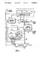
- FIG. 1is a block diagram of a test circuit in accordance with the invention.
- FIG. 2is a schematic block diagram of a portion of the test circuit shown in FIG. 1.
- a linear feedback shift register (LFSR) 5 for generating pseudo random test datacomprising a conventional shift register 10 coupled to an exclusive-or gate 13.
- a multiplexer circuit 15is adapted to selectively connect the input ports of a circuit under test 20 via a data bus 14 or to a data input bus 17 under control of signals 31 from control circuit 30.
- FIG. 2shows the LFSR 5 comprised of a 15-bit shift register 10 and an exclusive-or gate 13.
- the first 10 stages of the 15-bit shift registercorrespond to bit positions 1 to 10 and provide a 10 bit parallel output stream of pseudo random test data on data bus 14.
- the exclusive-or gate 13is connected to receive the values stored in two locations (e.g., 14th and 15th bit positions) of the 15-bit shift register and generates an exclusive-or feedback signal which is transmitted on feedback path 12 to the input stage of the shift register 10.
- the circuit under test 20receives the test patterns from the LFSR 5 and provides the test patterns on bus 22.
- the circuit of the inventionis particularly well suited to the testing of a circuit such as a switching network which of course comprises a plurality of transmission paths.
- the multiplexer 15is thus arranged to switchably connect the test signals from the LFSR 5 or the normal input data on bus 17 to the various input ports of the switching network.
- Data bus 21 connected to bus 22provides output data to other circuitry connected to the circuit under test 20.
- the data transmitted on data bus 21is either normal input data which originated on data bus 17 or the input test data originating from the LFSR 5.
- a second LFSR circuit 50is configured in a similar manner as the first; however, a multiplexer 40 permits one of two signals to be fed back to the input stage of a shift register 51.
- An exclusive-or gate 53is responsive to the two most significant bits of the shift register 51, (e.g., bits 14 and 15), to generate an exclusive-or feedback signal which is transmitted on feedback path 52 to the multiplexer 40 which is also connected to data line 24 to receive a signal carried on the least significant data line of data bus 22.
- the control circuit 30provides a selection control signal on control line 34 for selecting the signal carried on data line 24 or the feedback signal carried on feedback path 52.
- the least significant data line on data bus 22is connected to data line 24 to permit a portion of the pseudo random data transmitted in the least significant bit position to be transmitted to the second LFSR 50 via the multiplexer 40.
- the control circuitalso monitors the value stored in the LFSR 5 and the LFSR 50 via control lines 16 and 19 respectively.
- a comparator 60is connected to receive the 10-bit series of output test patterns from the circuit 20 and a 10-bit pattern generated by the second LFSR circuit 50 on data bus 58. The comparator 60 compares the two 10-bit series of test patterns and generates true or false signals.
- a clock signal provided on control line 18provides a timing signal to the first LFSR 5, the control circuit 30, the second LFSR circuit 50 and to the comparator 60. If that clock signal has the same frequency as that normally driving the circuit under test 20, then the circuit is exercised under real-life conditions.
- the LFSR 5is adapted to generate pseudo random binary test data for provision to the circuit under test 20. After a sequence of 2 15 -1 patterns have been generated by the LFSR 5 the sequence of patterns repeats.
- the control circuit 30Upon power up of the test circuitry, the control circuit 30 initializes the 15bit binary value stored in the LFSR 5 to a non-zero value to prevent the LFSR 5 from generating only zero-bit patterns. After initialization, the control circuit 30 continues to monitor the contents of the first and second LFSRs 5 and 50 to ensure that they do not remain in a state where either one of them contains all zero bits. If an all zero state is detected in the LFSR 5 or the LFSR 50, the control circuit 30 re-initializes the test circuit by asserting the signals on control lines 32 and 34.
- the binary word stored in the 15bit shift register 10is shifted in the more significant direction in a rotational manner; the bit stored in the first stage of the shift register 10 is shifted to the second stage; the bit stored in the second stage is simultaneously shifted to the third stage, and so on.
- Each shiftoccurs synchronously with each period of the clock signal.
- the bits stored in the two most significant bit positions, bits 14 and 15are exclusive-ored and the resultant signal is fed back to the least significant bit position of the shift register 10. Feeding back the resultant signal ensures that, with each period of the clock signal, the binary value of the 15-bit binary word in the LFSR 5 changes with each shift.
- the least significant 10 bits of the 15bit binary word corresponding to the first 10 stages of the shift registerform a binary pattern and with each shift, a different pattern is formed.
- the entire 15 bitscould be used to form test patterns, however, in the embodiment described only the least 10 significant bits are required.
- Providing an LFSR which has more register stages than the bits used for the test patterns as exemplified in the embodimentprovides more patterns in the series of test patterns and thus provides a greater variation of stimuli presented to the circuit under test.
- the series of pseudo random binary data patternsare transmitted to the circuit under test 20 via data bus 14 and multiplexer 15.
- the comparator 60is presented with the first pattern via data bus 22.
- the selection control signalis asserted on control line 34 to select a least significant bit of the series of patterns transmitted on data bus 22 to provide an input signal to the second LFSR circuit 50.
- a 15bit word corresponding to a word that was generated in the first LFSR 5will have been written into the second LFSR circuit 50.
- a 15-bit wordis captured which was generated sometime before in the first LFSR 5.
- the 15-bit binary word in the LFSR 50represents a seed value from which it may generate data patterns on its own in a free running mode.
- the control circuit 30thus de-asserts the selection control signal on control line 34 and the multiplexer 40 provides the input stage of the second LFSR 50 with the exclusive-or feedback signal carried on feedback path 52.
- a 10-bit binary word corresponding to the least significant 10-bits of the second LFSR 50are presented to the comparator 60.
- Each 10-bit binary word presented to the comparator 60 on data bus 58should henceforth match a pattern of the series of patterns received on data bus 22.
- a mismatch between the two 10-bit binary words presented to the comparator 60results in the comparator generating a false condition signal on an output line 62.
- a mismatchindicates that a 10-bit pseudo random binary pattern has become altered during transmission through the circuit under test 20. Corrective action may be taken on each error detection or statistics of false conditions may be logged and corrective action taken when the number of false conditions exceeds an acceptable predetermined
- the inventionthus provides a simple and economical circuit and method of verifying the integrity of a transmission path. Since the circuit uses only digital logic circuitry, it may be readily implemented as an integrated circuit either on its own or as a portion of another integrated circuit. In addition, the circuit may be driven by the same clock signal source as that of the circuit under test thus providing real life test conditions.
Landscapes
- Engineering & Computer Science (AREA)
- Computer Networks & Wireless Communication (AREA)
- Signal Processing (AREA)
- Tests Of Electronic Circuits (AREA)
- Maintenance And Management Of Digital Transmission (AREA)
- Dc Digital Transmission (AREA)
Abstract
Description
Claims (15)
Priority Applications (3)
| Application Number | Priority Date | Filing Date | Title |
|---|---|---|---|
| US07/651,835US5228042A (en) | 1991-02-07 | 1991-02-07 | Method and circuit for testing transmission paths |
| GB9201674AGB2252888B (en) | 1991-02-07 | 1992-01-27 | Method and circuit for testing transmission paths |
| JP4046114AJPH0583330A (en) | 1991-02-07 | 1992-01-31 | Method and apparatus for testing transmission line |
Applications Claiming Priority (1)
| Application Number | Priority Date | Filing Date | Title |
|---|---|---|---|
| US07/651,835US5228042A (en) | 1991-02-07 | 1991-02-07 | Method and circuit for testing transmission paths |
Publications (1)
| Publication Number | Publication Date |
|---|---|
| US5228042Atrue US5228042A (en) | 1993-07-13 |
Family
ID=24614420
Family Applications (1)
| Application Number | Title | Priority Date | Filing Date |
|---|---|---|---|
| US07/651,835Expired - LifetimeUS5228042A (en) | 1991-02-07 | 1991-02-07 | Method and circuit for testing transmission paths |
Country Status (3)
| Country | Link |
|---|---|
| US (1) | US5228042A (en) |
| JP (1) | JPH0583330A (en) |
| GB (1) | GB2252888B (en) |
Cited By (43)
| Publication number | Priority date | Publication date | Assignee | Title |
|---|---|---|---|---|
| US5347522A (en)* | 1990-07-13 | 1994-09-13 | Fujitsu Limited | Method and apparatus for detecting pseudo noise pattern for remote loopback test |
| US5383177A (en)* | 1993-09-20 | 1995-01-17 | Fujitsu Limited | Packet switching testing method and apparatus |
| US5392298A (en)* | 1991-07-11 | 1995-02-21 | Nec Corporation | Testing apparatus for exactly discriminating defective product from acceptable product and testing method used therein |
| US5394486A (en)* | 1992-08-06 | 1995-02-28 | De La Rue Giori S.A. | Method and apparatus for monitoring image processing operations |
| US5473619A (en)* | 1991-04-08 | 1995-12-05 | Sharp Kabushiki Kaisha | Method and apparatus for testing a driving circuit |
| US5490150A (en)* | 1992-09-18 | 1996-02-06 | At&T Corp. | Method and apparatus for data parity in a transmission system |
| US5541934A (en)* | 1993-10-04 | 1996-07-30 | Convex Computer Corporation | Apparatus, systems and methods for isolating faults during data transmission using parity |
| US5638004A (en)* | 1995-05-16 | 1997-06-10 | The United States Of America As Represented By The Secretary Of The Navy | Multiconductor continuity and intermittent fault analyzer with dynamic stimulation |
| US5675588A (en)* | 1993-09-20 | 1997-10-07 | Fujitsu Limited | Testing apparatus for transmission system |
| US5802073A (en)* | 1994-09-23 | 1998-09-01 | Vlsi Technology, Inc. | Built-in self test functional system block for UTOPIA interface |
| US5923677A (en)* | 1996-04-11 | 1999-07-13 | Sony Corporation | Method and apparatus for detecting failures between circuits |
| FR2786580A1 (en)* | 1998-11-30 | 2000-06-02 | St Microelectronics Sa | Circuit for generation of a signature for use in validating data arising from integrated circuits as used in transponder circuits in smart cards, car keys, etc., the circuit being small and having low power consumption |
| EP1241823A1 (en)* | 2001-03-06 | 2002-09-18 | Agilent Technologies Inc. a Delaware Corporation | Data communication system with self-test facility |
| US20020133763A1 (en)* | 2001-03-16 | 2002-09-19 | Agilent Technologies, Inc. | Bit error rate measurement |
| WO2002093821A1 (en)* | 2001-05-15 | 2002-11-21 | Koninklijke Philips Electronics N.V. | Device for testing the conformity of an electronic connection |
| US6518813B1 (en)* | 1999-01-29 | 2003-02-11 | Seiko Epson Corporation | Clock generating circuit and semiconductor integrated circuit using the same |
| US20030056052A1 (en)* | 2001-09-19 | 2003-03-20 | Koninklijke Philips Electronics N.V. | Data communication bus traffic generator arrangement |
| US20030084385A1 (en)* | 2001-02-02 | 2003-05-01 | Jared Zerbe | Method and apparatus for evaluating and optimizing a signaling system |
| US6574758B1 (en) | 2000-03-10 | 2003-06-03 | Cisco Technology, Inc. | Testing a bus coupled between two electronic devices |
| US20030179777A1 (en)* | 2001-07-31 | 2003-09-25 | Denton I. Claude | Method and apparatus for programmable generation of traffic streams |
| US20040047408A1 (en)* | 2002-09-10 | 2004-03-11 | Ingo Koenenkamp | Data link analyzer |
| US6735731B2 (en) | 2001-03-09 | 2004-05-11 | International Business Machines Corporation | Architecture for built-in self-test of parallel optical transceivers |
| EP1460793A1 (en)* | 2003-03-19 | 2004-09-22 | Synthesys Research, Inc. | A method and apparatus for counting the errors of a data signal that are outside the limits of an eye mask |
| US20040264615A1 (en)* | 2003-05-20 | 2004-12-30 | Andrew Ho | Margin test methods and circuits |
| US6873939B1 (en) | 2001-02-02 | 2005-03-29 | Rambus Inc. | Method and apparatus for evaluating and calibrating a signaling system |
| US20050076280A1 (en)* | 2003-10-03 | 2005-04-07 | Martinez Antonio Marroig | Programmable built-in self-test circuit for serializer/deserializer circuits and method |
| US20050154953A1 (en)* | 2004-01-12 | 2005-07-14 | Norskog Allen C. | Multiple function pattern generator and comparator having self-seeding test function |
| US20050154946A1 (en)* | 2003-12-31 | 2005-07-14 | Mitbander Suneel G. | Programmable measurement mode for a serial point to point link |
| EP1560034A1 (en)* | 2004-02-02 | 2005-08-03 | Synthesys Research, Inc. | A method and apparatus to measure and display data dependent eye diagrams |
| US20050259774A1 (en)* | 2004-05-18 | 2005-11-24 | Garlepp Bruno W | Statistical margin test methods and circuits |
| US6973297B1 (en) | 1999-09-01 | 2005-12-06 | Sirific Wireless Corporation | Method and apparatus for down-conversion of radio frequency (RF) signals with reduced local oscillator leakage |
| US20060168483A1 (en)* | 2005-01-24 | 2006-07-27 | Sherlock Derek A | On-chip circuitry for bus validation |
| US20060224339A1 (en)* | 2003-02-11 | 2006-10-05 | Dennis Kim | Circuit, apparatus and method for capturing a representation of a waveform from a clock-data recovery (CDR) unit |
| US20060242524A1 (en)* | 2005-02-17 | 2006-10-26 | International Business Machines Corporation | System and method for system-on-chip interconnect verification |
| US20070011534A1 (en)* | 2004-02-12 | 2007-01-11 | International Business Machines Corporation | Self-synchronising bit error analyser and circuit |
| US20070165472A1 (en)* | 2001-02-02 | 2007-07-19 | Rambus Inc. | Method and apparatus for evaluating and optimizing a signaling system |
| US20080010576A1 (en)* | 2006-06-27 | 2008-01-10 | Masayuki Urabe | Method for at speed testing of devices |
| US20080040639A1 (en)* | 2006-08-09 | 2008-02-14 | Unitest Inc. | Apparatus and Method For Generating Test Pattern Data For Testing Semiconductor Device |
| US7424075B2 (en) | 2003-07-31 | 2008-09-09 | Crossroads Systems, Inc. | Pseudorandom data pattern verifier with automatic synchronization |
| US20080240219A1 (en)* | 2003-05-20 | 2008-10-02 | Chen Fred F | Methods And Circuits For Performing Margining Tests In The Presence Of A Decision Feedback Equalizer |
| US20090222696A1 (en)* | 2008-02-28 | 2009-09-03 | International Business Machines Corporation | System and method for detecting non-reproducible pseudo-random test cases |
| US20100060779A1 (en)* | 2008-09-09 | 2010-03-11 | Sony Corporation | Light quantity detecting apparatus and imaging apparatus |
| US20110026421A1 (en)* | 2009-07-29 | 2011-02-03 | Qualcomm Incorporated | Adaptive transmissions in coordinated multiple point communications |
Families Citing this family (6)
| Publication number | Priority date | Publication date | Assignee | Title |
|---|---|---|---|---|
| JPH06295285A (en)* | 1993-02-15 | 1994-10-21 | Tokyo Electric Co Ltd | Interface device and printer using this device |
| EP0924891A1 (en) | 1997-12-15 | 1999-06-23 | Hewlett-Packard Company | Identification of framing symbols in a test signal |
| GB0321641D0 (en)* | 2003-09-16 | 2003-10-15 | Agilent Technologies Inc | Methods and apparatus for measuring service disruption |
| US7652975B2 (en)* | 2006-02-03 | 2010-01-26 | Agilent Technologies, Inc. | Interoperability verification for implementation according to communication standard |
| KR101187571B1 (en) | 2010-12-28 | 2012-10-05 | 주식회사 실리콘웍스 | Method of data transmission of Timing Controller and Source Driver added Bit Error Rate Tester and Device thereof |
| US8689357B2 (en)* | 2012-05-19 | 2014-04-01 | Freescale Semiconductor, Inc. | Tamper detector for secure module |
Citations (2)
| Publication number | Priority date | Publication date | Assignee | Title |
|---|---|---|---|---|
| US4827476A (en)* | 1987-04-16 | 1989-05-02 | Tandem Computers Incorporated | Scan test apparatus for digital systems having dynamic random access memory |
| US5001713A (en)* | 1989-02-08 | 1991-03-19 | Texas Instruments Incorporated | Event qualified testing architecture for integrated circuits |
Family Cites Families (1)
| Publication number | Priority date | Publication date | Assignee | Title |
|---|---|---|---|---|
| DE3047239C2 (en)* | 1980-12-16 | 1982-12-30 | Wandel & Goltermann Gmbh & Co, 7412 Eningen | Method and circuit arrangement for measuring the quality of digital transmission links and devices |
- 1991
- 1991-02-07USUS07/651,835patent/US5228042A/ennot_activeExpired - Lifetime
- 1992
- 1992-01-27GBGB9201674Apatent/GB2252888B/ennot_activeExpired - Fee Related
- 1992-01-31JPJP4046114Apatent/JPH0583330A/enactivePending
Patent Citations (2)
| Publication number | Priority date | Publication date | Assignee | Title |
|---|---|---|---|---|
| US4827476A (en)* | 1987-04-16 | 1989-05-02 | Tandem Computers Incorporated | Scan test apparatus for digital systems having dynamic random access memory |
| US5001713A (en)* | 1989-02-08 | 1991-03-19 | Texas Instruments Incorporated | Event qualified testing architecture for integrated circuits |
Cited By (100)
| Publication number | Priority date | Publication date | Assignee | Title |
|---|---|---|---|---|
| US5347522A (en)* | 1990-07-13 | 1994-09-13 | Fujitsu Limited | Method and apparatus for detecting pseudo noise pattern for remote loopback test |
| US5473619A (en)* | 1991-04-08 | 1995-12-05 | Sharp Kabushiki Kaisha | Method and apparatus for testing a driving circuit |
| US5392298A (en)* | 1991-07-11 | 1995-02-21 | Nec Corporation | Testing apparatus for exactly discriminating defective product from acceptable product and testing method used therein |
| US5394486A (en)* | 1992-08-06 | 1995-02-28 | De La Rue Giori S.A. | Method and apparatus for monitoring image processing operations |
| US5490150A (en)* | 1992-09-18 | 1996-02-06 | At&T Corp. | Method and apparatus for data parity in a transmission system |
| US5675588A (en)* | 1993-09-20 | 1997-10-07 | Fujitsu Limited | Testing apparatus for transmission system |
| US5383177A (en)* | 1993-09-20 | 1995-01-17 | Fujitsu Limited | Packet switching testing method and apparatus |
| US5541934A (en)* | 1993-10-04 | 1996-07-30 | Convex Computer Corporation | Apparatus, systems and methods for isolating faults during data transmission using parity |
| US5802073A (en)* | 1994-09-23 | 1998-09-01 | Vlsi Technology, Inc. | Built-in self test functional system block for UTOPIA interface |
| US5638004A (en)* | 1995-05-16 | 1997-06-10 | The United States Of America As Represented By The Secretary Of The Navy | Multiconductor continuity and intermittent fault analyzer with dynamic stimulation |
| US5923677A (en)* | 1996-04-11 | 1999-07-13 | Sony Corporation | Method and apparatus for detecting failures between circuits |
| FR2786580A1 (en)* | 1998-11-30 | 2000-06-02 | St Microelectronics Sa | Circuit for generation of a signature for use in validating data arising from integrated circuits as used in transponder circuits in smart cards, car keys, etc., the circuit being small and having low power consumption |
| EP1017195A1 (en)* | 1998-11-30 | 2000-07-05 | STMicroelectronics SA | Signature generation circuit |
| US6300791B1 (en) | 1998-11-30 | 2001-10-09 | Stmicroelectronics S.A. | Signature generator circuit |
| US6518813B1 (en)* | 1999-01-29 | 2003-02-11 | Seiko Epson Corporation | Clock generating circuit and semiconductor integrated circuit using the same |
| US7046980B1 (en) | 1999-09-01 | 2006-05-16 | Sirific Wireless Corporation | Method and apparatus for up-and down-conversion of radio frequency (RF) signals |
| US7016662B1 (en) | 1999-09-01 | 2006-03-21 | Sirific Wireless Corporation | Method and apparatus for up-conversion of radio frequency (RF) signals |
| US6973297B1 (en) | 1999-09-01 | 2005-12-06 | Sirific Wireless Corporation | Method and apparatus for down-conversion of radio frequency (RF) signals with reduced local oscillator leakage |
| US6574758B1 (en) | 2000-03-10 | 2003-06-03 | Cisco Technology, Inc. | Testing a bus coupled between two electronic devices |
| US7490275B2 (en) | 2001-02-02 | 2009-02-10 | Rambus Inc. | Method and apparatus for evaluating and optimizing a signaling system |
| US8812919B2 (en)* | 2001-02-02 | 2014-08-19 | Rambus Inc. | Method and apparatus for evaluating and optimizing a signaling system |
| US9356743B2 (en)* | 2001-02-02 | 2016-05-31 | Rambus Inc. | Method and apparatus for evaluating and optimizing a signaling system |
| US20030208707A9 (en)* | 2001-02-02 | 2003-11-06 | Jared Zerbe | Method and apparatus for evaluating and optimizing a signaling system |
| US20150078426A1 (en)* | 2001-02-02 | 2015-03-19 | Rambus Inc. | Method And Apparatus For Evaluating And Optimizing A Signaling System |
| US7360127B2 (en)* | 2001-02-02 | 2008-04-15 | Rambus Inc. | Method and apparatus for evaluating and optimizing a signaling system |
| US6873939B1 (en) | 2001-02-02 | 2005-03-29 | Rambus Inc. | Method and apparatus for evaluating and calibrating a signaling system |
| US8069378B2 (en)* | 2001-02-02 | 2011-11-29 | Rambus Inc. | Method and apparatus for evaluating and optimizing a signaling system |
| US8756469B2 (en)* | 2001-02-02 | 2014-06-17 | Rambus Inc. | Method and apparatus for evaluating and optimizing a signaling system |
| US7137048B2 (en)* | 2001-02-02 | 2006-11-14 | Rambus Inc. | Method and apparatus for evaluating and optimizing a signaling system |
| US20060236183A1 (en)* | 2001-02-02 | 2006-10-19 | Rambus Inc. | Method and apparatus for evaluating and optimizing a signaling system |
| US20070165472A1 (en)* | 2001-02-02 | 2007-07-19 | Rambus Inc. | Method and apparatus for evaluating and optimizing a signaling system |
| US8812918B2 (en) | 2001-02-02 | 2014-08-19 | Rambus Inc. | Method and apparatus for evaluating and optimizing a signaling system |
| US20100251040A1 (en)* | 2001-02-02 | 2010-09-30 | Rambus Inc. | Method and apparatus for evaluating and optimizing a signaling system |
| US10855413B2 (en) | 2001-02-02 | 2020-12-01 | Rambus Inc. | Method and apparatus for evaluating and optimizing a signaling system |
| US20030084385A1 (en)* | 2001-02-02 | 2003-05-01 | Jared Zerbe | Method and apparatus for evaluating and optimizing a signaling system |
| US6862701B2 (en) | 2001-03-06 | 2005-03-01 | Agilent Technologies, Inc. | Data communication system with self-test facility |
| EP1241823A1 (en)* | 2001-03-06 | 2002-09-18 | Agilent Technologies Inc. a Delaware Corporation | Data communication system with self-test facility |
| US6735731B2 (en) | 2001-03-09 | 2004-05-11 | International Business Machines Corporation | Architecture for built-in self-test of parallel optical transceivers |
| US20020133763A1 (en)* | 2001-03-16 | 2002-09-19 | Agilent Technologies, Inc. | Bit error rate measurement |
| US7389450B2 (en)* | 2001-03-16 | 2008-06-17 | Agilent Technologies Inc. | Bit error rate measurement |
| US20040128603A1 (en)* | 2001-05-15 | 2004-07-01 | Jacques Reberga | Device for testing the conformity of an electronic connection |
| WO2002093821A1 (en)* | 2001-05-15 | 2002-11-21 | Koninklijke Philips Electronics N.V. | Device for testing the conformity of an electronic connection |
| US7804782B2 (en)* | 2001-07-31 | 2010-09-28 | Denton I Claude | Method and apparatus for programmable generation of traffic streams |
| US7184408B2 (en)* | 2001-07-31 | 2007-02-27 | Denton I Claude | Method and apparatus for programmable generation of traffic streams |
| US20030179777A1 (en)* | 2001-07-31 | 2003-09-25 | Denton I. Claude | Method and apparatus for programmable generation of traffic streams |
| US20060280124A1 (en)* | 2001-07-31 | 2006-12-14 | Null Networks Llc | Method and apparatus for programmable generation of traffic streams |
| US20070008897A1 (en)* | 2001-07-31 | 2007-01-11 | Denton I Claude | Method and apparatus for programmable generation of traffic streams |
| US8072891B2 (en)* | 2001-07-31 | 2011-12-06 | Null Networks Llc | Method and apparatus for programmable generation of traffic streams |
| US20030056052A1 (en)* | 2001-09-19 | 2003-03-20 | Koninklijke Philips Electronics N.V. | Data communication bus traffic generator arrangement |
| US7020807B2 (en)* | 2001-09-19 | 2006-03-28 | Koninklijke Philips Electronics N.V. | Data communication bus traffic generator arrangement |
| WO2003032652A3 (en)* | 2001-10-12 | 2006-08-17 | Rambus Inc | Method and apparatus for evaluating and optimizing a signaling system |
| EP2253964A3 (en)* | 2001-10-12 | 2011-03-09 | Rambus Inc. | Method and apparatus for evaluating and optimizing a signaling system |
| US20040047408A1 (en)* | 2002-09-10 | 2004-03-11 | Ingo Koenenkamp | Data link analyzer |
| US7765074B2 (en) | 2003-02-11 | 2010-07-27 | Rambus Inc. | Circuit, apparatus and method for capturing a representation of a waveform from a clock-data recovery (CDR) unit |
| US20060224339A1 (en)* | 2003-02-11 | 2006-10-05 | Dennis Kim | Circuit, apparatus and method for capturing a representation of a waveform from a clock-data recovery (CDR) unit |
| EP1460793A1 (en)* | 2003-03-19 | 2004-09-22 | Synthesys Research, Inc. | A method and apparatus for counting the errors of a data signal that are outside the limits of an eye mask |
| US7627029B2 (en) | 2003-05-20 | 2009-12-01 | Rambus Inc. | Margin test methods and circuits |
| US8385492B2 (en) | 2003-05-20 | 2013-02-26 | Rambus Inc. | Receiver circuit architectures |
| US9116810B2 (en) | 2003-05-20 | 2015-08-25 | Rambus Inc. | Margin test methods and circuits |
| US11233589B2 (en) | 2003-05-20 | 2022-01-25 | Rambus Inc. | Margin test methods and circuits |
| US20080240219A1 (en)* | 2003-05-20 | 2008-10-02 | Chen Fred F | Methods And Circuits For Performing Margining Tests In The Presence Of A Decision Feedback Equalizer |
| US10880022B1 (en) | 2003-05-20 | 2020-12-29 | Rambus Inc. | Margin test methods and circuits |
| US10193642B2 (en) | 2003-05-20 | 2019-01-29 | Rambus Inc. | Margin test methods and circuits |
| US8817932B2 (en) | 2003-05-20 | 2014-08-26 | Rambus Inc. | Margin test methods and circuits |
| US10735116B2 (en) | 2003-05-20 | 2020-08-04 | Rambus Inc. | Margin test methods and circuits |
| US7596175B2 (en) | 2003-05-20 | 2009-09-29 | Rambus Inc. | Methods and circuits for performing margining tests in the presence of a decision feedback equalizer |
| US20040264615A1 (en)* | 2003-05-20 | 2004-12-30 | Andrew Ho | Margin test methods and circuits |
| US9544071B2 (en) | 2003-05-20 | 2017-01-10 | Rambus Inc. | Margin test methods and circuits |
| US7424075B2 (en) | 2003-07-31 | 2008-09-09 | Crossroads Systems, Inc. | Pseudorandom data pattern verifier with automatic synchronization |
| US20050076280A1 (en)* | 2003-10-03 | 2005-04-07 | Martinez Antonio Marroig | Programmable built-in self-test circuit for serializer/deserializer circuits and method |
| US7275195B2 (en)* | 2003-10-03 | 2007-09-25 | Avago Technologies General Ip (Singapore) Pte. Ltd. | Programmable built-in self-test circuit for serializer/deserializer circuits and method |
| US20050154946A1 (en)* | 2003-12-31 | 2005-07-14 | Mitbander Suneel G. | Programmable measurement mode for a serial point to point link |
| US7444558B2 (en)* | 2003-12-31 | 2008-10-28 | Intel Corporation | Programmable measurement mode for a serial point to point link |
| US20050154953A1 (en)* | 2004-01-12 | 2005-07-14 | Norskog Allen C. | Multiple function pattern generator and comparator having self-seeding test function |
| EP1560034A1 (en)* | 2004-02-02 | 2005-08-03 | Synthesys Research, Inc. | A method and apparatus to measure and display data dependent eye diagrams |
| US7404115B2 (en)* | 2004-02-12 | 2008-07-22 | International Business Machines Corporation | Self-synchronising bit error analyser and circuit |
| US7661039B2 (en)* | 2004-02-12 | 2010-02-09 | International Business Machines Corporation | Self-synchronizing bit error analyzer and circuit |
| US20070011534A1 (en)* | 2004-02-12 | 2007-01-11 | International Business Machines Corporation | Self-synchronising bit error analyser and circuit |
| US20090019326A1 (en)* | 2004-02-12 | 2009-01-15 | Gerard Boudon | Self-synchronizing bit error analyzer and circuit |
| US7336749B2 (en) | 2004-05-18 | 2008-02-26 | Rambus Inc. | Statistical margin test methods and circuits |
| US20050259774A1 (en)* | 2004-05-18 | 2005-11-24 | Garlepp Bruno W | Statistical margin test methods and circuits |
| US20060168483A1 (en)* | 2005-01-24 | 2006-07-27 | Sherlock Derek A | On-chip circuitry for bus validation |
| US7610526B2 (en) | 2005-01-24 | 2009-10-27 | Hewlett-Packard Development Company, L.P. | On-chip circuitry for bus validation |
| US20080215945A1 (en)* | 2005-02-17 | 2008-09-04 | International Business Machines Corporation | System and method for system-on-chip interconnect verification |
| US7865789B2 (en)* | 2005-02-17 | 2011-01-04 | International Business Machines Corporation | System and method for system-on-chip interconnect verification |
| US7313738B2 (en)* | 2005-02-17 | 2007-12-25 | International Business Machines Corporation | System and method for system-on-chip interconnect verification |
| US20060242524A1 (en)* | 2005-02-17 | 2006-10-26 | International Business Machines Corporation | System and method for system-on-chip interconnect verification |
| US20080010576A1 (en)* | 2006-06-27 | 2008-01-10 | Masayuki Urabe | Method for at speed testing of devices |
| US20100153801A1 (en)* | 2006-06-27 | 2010-06-17 | Masayuki Urabe | Method for at speed testing of devices |
| US8214706B2 (en)* | 2006-06-27 | 2012-07-03 | Marvell International Ltd. | Method and apparatus for testing an electronic circuit integrated with a semiconductor device |
| US7673207B2 (en)* | 2006-06-27 | 2010-03-02 | Marvell International Ltd. | Method for at speed testing of devices |
| US20080040639A1 (en)* | 2006-08-09 | 2008-02-14 | Unitest Inc. | Apparatus and Method For Generating Test Pattern Data For Testing Semiconductor Device |
| US20090222696A1 (en)* | 2008-02-28 | 2009-09-03 | International Business Machines Corporation | System and method for detecting non-reproducible pseudo-random test cases |
| US7774668B2 (en) | 2008-02-28 | 2010-08-10 | International Business Machines Corporation | System and method for detecting non-reproducible pseudo-random test cases |
| US20100060779A1 (en)* | 2008-09-09 | 2010-03-11 | Sony Corporation | Light quantity detecting apparatus and imaging apparatus |
| US8279326B2 (en)* | 2008-09-09 | 2012-10-02 | Sony Corporation | Light quantity detecting apparatus and imaging apparatus |
| CN102474474B (en)* | 2009-07-29 | 2015-08-26 | 高通股份有限公司 | Adaptive Transmission in Coordinated Multipoint Communication |
| US9172561B2 (en) | 2009-07-29 | 2015-10-27 | Qualcomm Incorporated | Adaptive transmissions in coordinated multiple point communications |
| CN102474474A (en)* | 2009-07-29 | 2012-05-23 | 高通股份有限公司 | Adaptive Transmission in Coordinated Multipoint Communication |
| US20110026421A1 (en)* | 2009-07-29 | 2011-02-03 | Qualcomm Incorporated | Adaptive transmissions in coordinated multiple point communications |
Also Published As
| Publication number | Publication date |
|---|---|
| GB2252888B (en) | 1995-08-16 |
| GB9201674D0 (en) | 1992-03-11 |
| GB2252888A (en) | 1992-08-19 |
| JPH0583330A (en) | 1993-04-02 |
Similar Documents
| Publication | Publication Date | Title |
|---|---|---|
| US5228042A (en) | Method and circuit for testing transmission paths | |
| US5485470A (en) | Communication circuit fault detector | |
| US7062696B2 (en) | Algorithmic test pattern generator, with built-in-self-test (BIST) capabilities, for functional testing of a circuit | |
| US7661039B2 (en) | Self-synchronizing bit error analyzer and circuit | |
| US7219113B2 (en) | Pseudo-random binary sequence checker with automatic synchronization | |
| US5726991A (en) | Integral bit error rate test system for serial data communication links | |
| US7464307B2 (en) | High performance serial bus testing methodology | |
| US6667993B1 (en) | Communication channel | |
| US7788562B2 (en) | Pattern controlled, full speed ATE compare capability for deterministic and non-deterministic IC data | |
| US4216374A (en) | Hybrid signature test method and apparatus | |
| US20050076280A1 (en) | Programmable built-in self-test circuit for serializer/deserializer circuits and method | |
| US8572447B2 (en) | Circuitry for built-in self-test | |
| CN101485146A (en) | Loopback module based on high-speed serial crossbar switch | |
| EP0918227B1 (en) | Automatic circuit tester having a waveform acquisition mode of operation | |
| US4713605A (en) | Linear feedback shift register for circuit design technology validation | |
| US7017098B2 (en) | Built-in self-test for multi-channel transceivers without data alignment | |
| NO152070B (en) | DEVICE FOR TESTING ONE OR MORE DIGITAL CIRCUITS | |
| CA2057447C (en) | Method and circuit for testing transmission paths | |
| GB2146205A (en) | Jitter circuits; assessing jitter performance | |
| US8065597B1 (en) | Self test of plesiochronous interconnect | |
| KR19980032311A (en) | Pulse Generation on Analog Channels of Automatic Test Unit (ATE) Testers | |
| JPH07154258A (en) | Method and equipment for testing a/d converter | |
| US5072448A (en) | Quasi-random digital sequence detector | |
| US7424075B2 (en) | Pseudorandom data pattern verifier with automatic synchronization | |
| SU1691841A1 (en) | A digital installations tester |
Legal Events
| Date | Code | Title | Description |
|---|---|---|---|
| AS | Assignment | Owner name:BELL-NORTHERN RESEARCH LTD., CANADA Free format text:ASSIGNMENT OF ASSIGNORS INTEREST.;ASSIGNORS:GAUTHIER, JOHN A.;GOATCHER, JOHN K.;REEL/FRAME:005654/0945;SIGNING DATES FROM 19910102 TO 19910107 Owner name:NORTHERN TELECOM LIMITED, P.O. BOX 6123, STATION A Free format text:ASSIGNMENT OF ASSIGNORS INTEREST.;ASSIGNOR:BELL-NORTHERN RESEARCH LTD.;REEL/FRAME:005647/0996 Effective date:19910122 Owner name:NORTHERN TELECOM LIMITED, P.O. BOX 6123, STATION A Free format text:ASSIGNMENT OF ASSIGNORS INTEREST.;ASSIGNOR:BELL-NORTHERN RESEARCH LTD.;REEL/FRAME:005647/0997 Effective date:19910122 | |
| STCF | Information on status: patent grant | Free format text:PATENTED CASE | |
| FPAY | Fee payment | Year of fee payment:4 | |
| AS | Assignment | Owner name:NORTEL NETWORKS CORPORATION, CANADA Free format text:CHANGE OF NAME;ASSIGNOR:NORTHERN TELECOM LIMITED;REEL/FRAME:010567/0001 Effective date:19990429 | |
| AS | Assignment | Owner name:NORTEL NETWORKS LIMITED, CANADA Free format text:CHANGE OF NAME;ASSIGNOR:NORTEL NETWORKS CORPORATION;REEL/FRAME:011195/0706 Effective date:20000830 Owner name:NORTEL NETWORKS LIMITED,CANADA Free format text:CHANGE OF NAME;ASSIGNOR:NORTEL NETWORKS CORPORATION;REEL/FRAME:011195/0706 Effective date:20000830 | |
| FPAY | Fee payment | Year of fee payment:8 | |
| FPAY | Fee payment | Year of fee payment:12 | |
| SULP | Surcharge for late payment | Year of fee payment:11 | |
| AS | Assignment | Owner name:INDEPENDENCE MANZANAR LLC, NEVADA Free format text:ASSIGNMENT OF ASSIGNORS INTEREST;ASSIGNOR:NORTEL NETWORKS LIMITED;REEL/FRAME:017286/0465 Effective date:20050406 |