US5219226A - Imaging and temperature monitoring system - Google Patents
Imaging and temperature monitoring systemDownload PDFInfo
- Publication number
- US5219226A US5219226AUS07/782,262US78226291AUS5219226AUS 5219226 AUS5219226 AUS 5219226AUS 78226291 AUS78226291 AUS 78226291AUS 5219226 AUS5219226 AUS 5219226A
- Authority
- US
- United States
- Prior art keywords
- temperature
- area
- image
- pyrometer
- output
- Prior art date
- Legal status (The legal status is an assumption and is not a legal conclusion. Google has not performed a legal analysis and makes no representation as to the accuracy of the status listed.)
- Expired - Lifetime
Links
Images


Classifications
- G—PHYSICS
- G01—MEASURING; TESTING
- G01J—MEASUREMENT OF INTENSITY, VELOCITY, SPECTRAL CONTENT, POLARISATION, PHASE OR PULSE CHARACTERISTICS OF INFRARED, VISIBLE OR ULTRAVIOLET LIGHT; COLORIMETRY; RADIATION PYROMETRY
- G01J5/00—Radiation pyrometry, e.g. infrared or optical thermometry
- G01J5/02—Constructional details
- G01J5/07—Arrangements for adjusting the solid angle of collected radiation, e.g. adjusting or orienting field of view, tracking position or encoding angular position
- G—PHYSICS
- G01—MEASURING; TESTING
- G01J—MEASUREMENT OF INTENSITY, VELOCITY, SPECTRAL CONTENT, POLARISATION, PHASE OR PULSE CHARACTERISTICS OF INFRARED, VISIBLE OR ULTRAVIOLET LIGHT; COLORIMETRY; RADIATION PYROMETRY
- G01J5/00—Radiation pyrometry, e.g. infrared or optical thermometry
- G01J5/02—Constructional details
- G01J5/025—Interfacing a pyrometer to an external device or network; User interface
- G—PHYSICS
- G01—MEASURING; TESTING
- G01J—MEASUREMENT OF INTENSITY, VELOCITY, SPECTRAL CONTENT, POLARISATION, PHASE OR PULSE CHARACTERISTICS OF INFRARED, VISIBLE OR ULTRAVIOLET LIGHT; COLORIMETRY; RADIATION PYROMETRY
- G01J5/00—Radiation pyrometry, e.g. infrared or optical thermometry
- G01J5/02—Constructional details
- G01J5/08—Optical arrangements
- G01J5/0801—Means for wavelength selection or discrimination
- G—PHYSICS
- G01—MEASURING; TESTING
- G01J—MEASUREMENT OF INTENSITY, VELOCITY, SPECTRAL CONTENT, POLARISATION, PHASE OR PULSE CHARACTERISTICS OF INFRARED, VISIBLE OR ULTRAVIOLET LIGHT; COLORIMETRY; RADIATION PYROMETRY
- G01J5/00—Radiation pyrometry, e.g. infrared or optical thermometry
- G01J5/02—Constructional details
- G01J5/08—Optical arrangements
- G01J5/0806—Focusing or collimating elements, e.g. lenses or concave mirrors
- G—PHYSICS
- G01—MEASURING; TESTING
- G01J—MEASUREMENT OF INTENSITY, VELOCITY, SPECTRAL CONTENT, POLARISATION, PHASE OR PULSE CHARACTERISTICS OF INFRARED, VISIBLE OR ULTRAVIOLET LIGHT; COLORIMETRY; RADIATION PYROMETRY
- G01J5/00—Radiation pyrometry, e.g. infrared or optical thermometry
- G01J5/02—Constructional details
- G01J5/08—Optical arrangements
- G01J5/0813—Planar mirrors; Parallel phase plates
- G—PHYSICS
- G01—MEASURING; TESTING
- G01J—MEASUREMENT OF INTENSITY, VELOCITY, SPECTRAL CONTENT, POLARISATION, PHASE OR PULSE CHARACTERISTICS OF INFRARED, VISIBLE OR ULTRAVIOLET LIGHT; COLORIMETRY; RADIATION PYROMETRY
- G01J5/00—Radiation pyrometry, e.g. infrared or optical thermometry
- G01J5/02—Constructional details
- G01J5/08—Optical arrangements
- G01J5/084—Adjustable or slidable
- G—PHYSICS
- G01—MEASURING; TESTING
- G01J—MEASUREMENT OF INTENSITY, VELOCITY, SPECTRAL CONTENT, POLARISATION, PHASE OR PULSE CHARACTERISTICS OF INFRARED, VISIBLE OR ULTRAVIOLET LIGHT; COLORIMETRY; RADIATION PYROMETRY
- G01J5/00—Radiation pyrometry, e.g. infrared or optical thermometry
- G01J5/02—Constructional details
- G01J5/08—Optical arrangements
- G01J5/0846—Optical arrangements having multiple detectors for performing different types of detection, e.g. using radiometry and reflectometry channels
- G—PHYSICS
- G01—MEASURING; TESTING
- G01J—MEASUREMENT OF INTENSITY, VELOCITY, SPECTRAL CONTENT, POLARISATION, PHASE OR PULSE CHARACTERISTICS OF INFRARED, VISIBLE OR ULTRAVIOLET LIGHT; COLORIMETRY; RADIATION PYROMETRY
- G01J5/00—Radiation pyrometry, e.g. infrared or optical thermometry
- G01J5/02—Constructional details
- G01J5/08—Optical arrangements
- G01J5/0859—Sighting arrangements, e.g. cameras
- H—ELECTRICITY
- H04—ELECTRIC COMMUNICATION TECHNIQUE
- H04N—PICTORIAL COMMUNICATION, e.g. TELEVISION
- H04N23/00—Cameras or camera modules comprising electronic image sensors; Control thereof
- H04N23/10—Cameras or camera modules comprising electronic image sensors; Control thereof for generating image signals from different wavelengths
- H04N23/11—Cameras or camera modules comprising electronic image sensors; Control thereof for generating image signals from different wavelengths for generating image signals from visible and infrared light wavelengths
- G—PHYSICS
- G01—MEASURING; TESTING
- G01J—MEASUREMENT OF INTENSITY, VELOCITY, SPECTRAL CONTENT, POLARISATION, PHASE OR PULSE CHARACTERISTICS OF INFRARED, VISIBLE OR ULTRAVIOLET LIGHT; COLORIMETRY; RADIATION PYROMETRY
- G01J5/00—Radiation pyrometry, e.g. infrared or optical thermometry
- G01J5/02—Constructional details
- G01J5/04—Casings
- G01J5/047—Mobile mounting; Scanning arrangements
Definitions
- This inventionrelates generally to imaging systems and, more particularly, to systems for producing images of objects and for monitoring the temperature of the imaged objects.
- the efficiency and effectiveness of many industrial processesdepends on the temperatures at which the processes are performed. For example, a kiln's ability to harden or dry substances depends, at least in part, upon the kiln's temperature. Similarly, the efficiency of a furnace in converting fuel into thermal energy, and the ability of a recovery boiler to extract chemicals from waste material, is temperature-dependent.
- the temperature of the systemmust be monitored. Information is collected regarding the temperature of the area in which the process is actually being performed. This process area may include solid, liquid, and gaseous objects whose temperatures are to be measured. In some instances, a general indication of the temperature of the process area is desired. In other cases, information regarding the spatial distribution of temperature over the process area is needed.
- One of the simplest ways that information regarding the temperature of a process area can be obtainedis through direct visual observation of the area.
- the process areamust be sufficiently hot to emit radiation that can be seen by the operator.
- the temperature of the process areais then interpreted based upon the color or wavelength of the emitted radiation.
- the wavelengths and intensity of the emitted radiationdepend upon the temperature and material composition of objects included in the area.
- the wavelength corresponding to the peak spectral intensityis inversely proportional to temperature.
- Direct visual observationalso advantageously provides the operator with a good deal of nonthermal information that may be useful in controlling a process. For example, by directly viewing the process, an operator may be able to monitor objects whose location or size, rather than temperature, influence the process.
- the use of direct visual observation to monitor process temperaturedoes, however, have several limitations.
- the processmay take place at temperatures that are too high to allow direct visual observations to be easily or safely conducted. Further, direct visual observations often provide, at best, rough qualitative estimates of temperature that may be entirely inadequate for the required process control. In still other instances, temperature information must be collected from a number of sites, limiting the ability of a single individual to directly observe the operation at each site.
- a simple systemincludes a camera connected to a remote monitor or display.
- the camerafocuses radiation from the process area to produce an optical image that is converted to a video image of the area.
- an infrared cameramay be used to produce a video image representative of the intensity of received infrared radiation and, hence, the temperature of the viewed area.
- the video imageis transferred to the monitor for display.
- An operator viewing the monitorcan then make a qualitative assessment of the way in which temperature varies over the imaged area.
- Temperature monitoring systemshave also been developed to provide quantitative or absolute temperature measurements.
- One example of such a systemis the product sold by the assignee of the present application, Quadtek, Inc., under the trademark M702.
- the M702 systemincludes a pyrometer that is integrated into an infrared camera, which is, in turn, coupled to a monitor. The position of the pyrometer, relative to the camera, is fixed.
- the camerareceives infrared radiation from the process area and provides a video output to the monitor.
- the pyrometeralso receives radiation from a limited region of the process area viewed by the camera and provides a pyrometer output to the monitor.
- the monitorresponds to the outputs from the camera and pyrometer by producing a displayed image of the process area and an indication of the temperature of the single region of the process area monitored by the pyrometer.
- the 7000-CTS systemis a scanning temperature measurement system, which includes an infrared thermometer and a television camera. Although the position of the thermometer relative to the camera is fixed, a scanning head allows the position of the combined thermometer and camera to be adjusted. The camera is used by the operator to sight the area whose temperature is monitored by the thermometer.
- thermometer systemdoes allow the temperature of more than one fixed region to be determined, it has several limitations. First, because both the thermometer and camera are scanned, a relatively large, bulky, and expensive scanning head is required. Further, due to the bulk of the scanned components, the scanning speed of the system is limited and may present problems when relatively continuous temperature information must be collected over large or dispersed regions of the area.
- the CALICO systemincludes a pyrometer, video imager, temperature analyzer, and monitor.
- the video imageris, for example, an infrared camera that produces a video image representing the intensity of infrared emissions received from the process area.
- the pyrometerproduces a reference temperature output in response to radiation received from a single reference region included in the area viewed by the infrared camera.
- the CALICO imager and pyrometerpass the video image and reference temperature data to the temperature analyzer.
- the temperature analyzerdetermines the shading or coloring of the portion of the video image associated with the reference region. The relationship between video shading and the measured reference temperature is then determined. As a result, the temperature analyzer is able to determine the absolute temperature of the imaged area at select regions of interest, other than the reference region viewed by the pyrometer, in the following manner.
- the temperature analyzerfirst determines the location of the select region of interest on the video image. The temperature analyzer then computes the temperature associated with the shading of the video image at this point. Because the relationship between shading and temperature has already been accurately defined for the reference point, that information can then be used to calibrate a determination of temperature based upon the shade of any other point on the video image.
- the output of the infrared camera of the CALICO systemis used both to generate a video image of the process area and to measure temperature.
- the pyrometersimply provides continuous calibration of the temperature measurements based upon the camera output. Because the camera is used both to image the area of interest and to monitor temperature, its performance can typically be optimized for only one of the two tasks.
- the camera output used for imagingit may be desirable to alter the shading of the video image to lighten or darken specific regions of the image for better visibility. If the camera output is also used for temperature measurement, however, such shading corrections might adversely influence the interpretation of temperature. Similarly, if the displayed image generally lacks sufficient contrast, the black level or contrast of the image can be offset accordingly. Again, however, such an adjustment might adversely influence temperature measurements based upon the same image.
- a camera having a nonlinear responsemay result in good image production, but skew temperature measurements.
- a camera having a linear responsemay provide a truer temperature measurement, but less useful image information.
- the minimum temperature that can be sensed by the CALICO systemis limited by the available wavelength range that conventional infrared cameras respond to. Because most conventional infrared cameras respond only to radiation shorter than 1.8 microns, the system is typically limited to monitoring temperatures above 1470 degrees Fahrenheit (800 degrees Centigrade).
- the systemincludes an imaging device for receiving radiation from the area of interest and producing an image output that represents an image of the area.
- the systemalso includes a temperature-sensitive device for receiving radiation from at least one of the select regions included in the area and producing a temperature output that represents the temperature of the one of the select regions.
- a controlleris included to control which of the at least one select regions radiation is received from by the temperature-sensitive device.
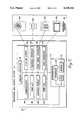
- FIG. 1is a block diagram of an imaging and temperature monitoring system constructed in accordance with this invention
- FIG. 2is a schematic illustration of a sensor head included in the system of FIG. 1;
- FIG. 3is an illustration of a translation stage that is used to adjust the position of a pyrometer included in the sensor head of FIG. 2;
- FIG. 4is an illustration of an alternative construction of the translation stage of FIG. 3;
- FIG. 5is an illustration of another alternative embodiment of the stage of FIG. 3;
- FIG. 6is a block diagram of a processing and control system and various peripheral devices included in the system of FIG. 1;
- FIG. 7is an illustration of a display generated by a monitor included among the peripheral devices of FIG. 6.
- the system 10includes a sensor head 12 that is exposed to an environment E.
- the sensor head 12provides outputs to a processing and control system 14 which, in turn, causes a visible image of environment E to be displayed by peripheral devices 16, along with information regarding the temperature of environment E.
- a processing and control system 14which, in turn, causes a visible image of environment E to be displayed by peripheral devices 16, along with information regarding the temperature of environment E.
- the construction of system 10advantageously allows both the visible image and the temperature information to be produced simply and with heretofore unachieved accuracy.
- the environment E that system 10 is used withwill be briefly considered.
- the present inventionis useful for providing image and temperature information relating to the status of, and processes carried out in, a variety of environments E.
- environments Emay include solid, liquid, and gaseous objects that are to be imaged and whose temperatures are to be measured.
- thermal energy of these objectsis typically radiated in the form of electromagnetic waves.
- This radiationmay include portions of both the visible and infrared segments of the electromagnetic spectrum. It is the analysis of this radiation that allows the temperature of the objects to be evaluated noninvasively, i.e., without requiring physical contact with environment E.
- radiation from a process area P included in environment Eis received by the sensor head 12, where it is converted to an optical image and then an electronic or video image of area P.
- the sensor head 12also uses at least a portion of the optical image to determine the temperature of one or more regions R located in the process area P.
- the video image and temperature dataare then transferred from the sensor head 12 to the processing and control system 14.
- the peripheral devices 16which are coupled to the processing and control system 14, display an image of the process area P for the operator of system 10.
- the peripheral devices 16also provide measurements of the absolute temperature of regions R of area P.
- Peripheral devices 16allow the operator to provide system 10 with various inputs necessary to initiate the desired operation of system 10.
- Process controls 18may also be included to regulate the operation of a process within environment E.
- controls 18receive temperature and, perhaps, image data from system 14 and analyze that data to determine the requisite adjustments to be made to the process.
- the process controls 18may also receive inputs from the operator via peripheral devices 16.
- sensor head 12includes a number of elements. Specifically, in a preferred arrangement, sensor head 12 includes a group of optical components 20, a pyrometer 22, an adjustable translation stage 24, a video imager 26, and electronics section 28.
- the optical components 20receive visible and infrared radiation from the process area P of environment E and provide an optical image of the process area P to pyrometer 22 and video imager 26.
- Optical components 20include objective lenses 30 and transfer lenses 32, fitted within a lens tube 34.
- Objective lenses 30preferably form a wide-angle element that allows an optical image of a relatively large process area P to be formed.
- the optical imageis transmitted from objective lenses 30 through the series of transfer lenses 32, which collect and collimate the image.
- Optical components 20also include a beam splitter 36 that splits the optical image formed by the components within lens tube 34 into two components. More particularly, depending upon the nature of the video imager used, beam splitter 36 reflects a visible or infrared wavelength component of the optical image along a first path I. An infrared wavelength component of the optical image also passes through beam splitter 36 and traverses a second path II.
- the portion of the optical image traversing path Ipasses through several additional optical components 20.
- a lens 38passes the image to a mirror 40, which reflects the image to video imager 26.
- Lens 38focuses the optical image for the entire viewed area on video imager 26.
- Mirror 40introduces a fold into path I to accommodate space restrictions within sensor head 12.
- the portion of the optical image traversing path IIalso passes through several additional optical components 20. Specifically, a lens 42 passes the image to an optical filter 44 before the image is received by pyrometer 22. Although lens 42 focuses the infrared portion of the optical image for the entire viewed area, as will be explained in greater detail below, the pyrometer detector is relatively small. Thus, only a portion of the path II optical image, corresponding to a single region R of the process area, actually impinges on the detector. By adjusting the relative alignment of pyrometer 22 and the focused optical image of the entire viewed area, however, radiation can be collected from various regions R within the imaged area. The filter 44 ensures that the radiation passed to pyrometer 22 has the appropriate spectral content.
- the characteristics of the various optical components 20can be varied depending upon the environment is which the system is intended to operate, as well the desired wavelengths involved in the image and temperature measurement processes.
- the various optical components 20, except lens 42 and filter 44are part of a closed-circuit television camera sold by Quadtek, Inc. under the trademark LYNX.
- the pyrometer 22is, for example, a radiation pyrometer. Pyrometer 22 measures the temperature of a hot object by focusing the thermal radiation emitted by the object.
- pyrometer 22is an optical radiation pyrometer, which evaluates the incandescent brightness of a hot object to determine the object's temperature. Pyrometer 22 produces a single output that effectively represents an average of the temperature of the viewed region R. As will be described in greater detail below, this output is used by the electronics section 28 to determine the region's temperature.
- Pyrometer 22includes a square sensor or detector that receives a portion of the focused optical image corresponding to a limited region R of the process area P. Pyrometer 22 has an effective field of view of 0.6 degrees by 0.6 degrees, when used in conjunction with optical components 20. Thus, pyrometer 22 normally views a region R representing roughly 0.01% of the process area P that is viewed. As will be described in greater detail below, however, in the preferred arrangement, pyrometer 22 is adjustably positioned for movement in a plane that is orthogonal to path II of the radiation, allowing it to receive radiation from different regions of the process area.
- pyrometer 22may advantageously be a one-color pyrometer or a two-color pyrometer.
- a one-color pyrometeris typically responsive to a limited band of radiation, corresponding to the pass band of filter 44. The output produced by such a one-color pyrometer is proportional to the intensity of the radiation received in that band.
- a pyrometer responsive to the middle of the infrared spectrummay be used in systems designed to measure temperatures in various ranges spanning 400-2600 degrees Fahrenheit (200-1430 degrees Centigrade).
- a two-color, or ratio, pyrometerproduces an output that is based upon the ratio of the intensity of the radiation received at two different wavelengths.
- a two-color pyrometermay be advantageously used in smoky or dusty environments, because the ratiometric analysis allows measurements to be made with relatively little disturbance by the smoke and dust.
- video imager 26receives the focused optical image of the process area P that is transferred along path I. Video imager 26 responds by generating an electronic or video image corresponding to the optical image of the viewed process area P.
- Video imager 26may be any one of a variety of devices, such as the camera tube of a television camera or a vidicon.
- One example of a suitable video imager 26is the Javelin JE2362A solid state camera including a solid state detector, available from Javelin Electronics of Torrance, Calif.
- stage 24moveably supports the pyrometer 22 relative to the focused optical image that is transmitted along path II by the optical components 20.
- stage 24includes a support structure 46, a pair of linear bearings 48 and 50, and a pair of linear stepper motors 52 and 54.
- the support structure 46is generally movable along x- and y-coordinate axes, as illustrated in FIG. 3.
- Support structure 46in formed by a support plate 56, x-coordinate side plate 58, and y-coordinate side plate 60, which may be fixedly secured together or machined from a single block of material.
- Pyrometer 22is attached to the rectangular support plate 56.
- the rectangular, x-coordinate side plate 58 and y-coordinate side plate 60extend normal to, and form a corner with, support plate 56.
- the linear bearings or ball slides 48 and 50are of the type sold by Pic Design under the part number PB04-05.
- the x-coordinate linear bearing 48is attached to the inner surface of the x-coordinate side plate 58. Specifically, bearing 48 extends along an axis parallel to support plate 56 and spaced-apart therefrom.
- the y-coordinate linear bearing 50is attached to the inner surface of the y-coordinate side plate 60. Bearing 50 extends along an axis parallel to support plate 56 and spaced-apart therefrom by a distance that is less than the spacing between bearing 48 and plate 56. As a result, bearings 48 and 50 are substantially perpendicular to each other.
- the linear stepper motors 52 and 54are of the type sold by HSI Inc. of Waterbury, Conn. under the part number 26841-05 and are fixedly mounted relative to sensor head 12.
- the x-coordinate stepper motor 52includes a shaft that extends normal to the y-coordinate side plate 60 and telescopes in and out in response to electrical inputs applied to motor 52. The projecting end of the shaft engages a mating surface of the y-coordinate bearing 50.
- the y-coordinate stepper motor 54includes a shaft, which extends normal to both x-coordinate side plate 58 and the shaft of motor 52 and telescopes in and out in response to electrical inputs to motor 54. The projecting end of the shaft of motor 54 engages a mating surface of x-coordinate bearing 48.
- the various components of translation stage 24cooperate to control the position of pyrometer 22 in the following manner.
- an inputis applied to the x-coordinate stepper motor 52.
- the shaft of motor 52extends or retracts, drawing the y-coordinate bearing 50 along with it in the x-direction.
- the y-coordinate bearing 48is fixedly attached to side plate 60 of structure 46, structure 46 and pyrometer 22 also are drawn in the x-direction.
- the end of the shaft of the y-coordinate stepper motor 54slides in the x-coordinate bearing 48, allowing the position of the y-coordinate stepper motor 54 relative to sensor head 12 to remain fixed.
- the input to the x-coordinate motor 52can be altered to control the extension of the shaft and, hence, the translation of stage 24.
- the y-coordinate motor 54 and bearing 48are similarly used to control motion of pyrometer 22 in the y-direction. By controlling the x- and y-coordinates of pyrometer 22, pyrometer 22 is thus able to selectively receive radiation from different regions R of the process area P.
- the translation stage 24may include a rectangular frame 62, provided with a crossbar 64 upon which pyrometer 22 is mounted.
- a first stepper motoris fixedly attached to frame 62 and is coupled to crossbar 64 by gears (not shown). The first motor and gears drive crossbar 64 relative to frame 62 along an x-axis.
- a second stepper motoris fixedly attached to crossbar 64 and coupled to a platform supporting pyrometer 22 by gears (not shown). The second motor and gears drive pyrometer 22 relative to crossbar 64 along a y-axis.
- pyrometer 22can be scanned in both the x-direction and the y-direction.
- the stage 24 shown in FIG. 3, however,is currently preferred because it is simpler and does not require one of the stepper motors to be mounted to a movable element (i.e., crossbar 64).
- the translation stage 24is constructed to fixedly support pyrometer 22.
- a scanning mirror assembly 66is positioned in path II.
- Assembly 66includes a mirror 68 that is gimbaled and driven by a support structure 70. By altering the orientation of mirror 68, the portion of the light traversing path II that impinges upon pyrometer 22 can be controlled.
- this arrangementallows scanning to be accomplished quite rapidly, it is more complex and expensive than the arrangement of FIG. 3.
- the electronics section 28includes a number of components. Specifically, positioning controls 76 are included to provide drive signals to stepper motors 52 and 54. Positioning controls 76 respond to inputs from a microcomputer 78, also included in electronics section 28, and provide appropriately conditioned drive signals to stepper motors 52 and 54. Stepper motors 52 and 54 then initiate the desired adjustments in the position of support structure 46 and pyrometer 22.
- At least one pyrometer amplifier 80is also included in electronics section 28.
- Amplifier 80is coupled to pyrometer 22 to amplify the analog output of pyrometer 22 suitably for further processing by, for example, an analog-to-digital (A/D) converter 82.
- the A/D converter 82converts the amplified analog output of pyrometer 22 into digital form for use by microcomputer 78 in determining the temperature of the viewed region R of the process area, as described in greater detail below.
- the microcomputer 78includes a central processing unit (CPU) 84, memory 86, and interfaces 88.
- Memory 86 of microcomputer 78is initially loaded with a program that is responsible for controlling the CPU's performance of several tasks.
- the programincludes a routine that controls the translation stage 24 and determines which portion of the radiation traversing path II will be received by pyrometer 22.
- the programanalyzes information regarding the present position of pyrometer 22, previously stored by CPU 84, as well as the desired change in the pyrometer's position, input via CPU 84 in response to information received from the processing and control system 14.
- CPU 84executes the routine to determine the outputs that must be produced by the positioning controls 76 to achieve the desired positional adjustment.
- a second routine stored in memory 86controls the determination of the temperature of the region R.
- a predetermined relationshipexists between pyrometer output and temperature for the particular type of pyrometer and process area P involved. This relationship is stored in memory 86 and is accessed by CPU 84 to determine the temperature of the region R in view of the output of pyrometer 22.
- a communications block 90included in electronics section 28, allows information to be efficiently transferred between sensor head 12 and processing and control system 14.
- communications block 90preferably includes a multiplexer to multiplex the video output of imager 26 and the digitally processed output of pyrometer 22 for transmission to the processing and control system 14.
- the multiplexing of video and temperature data onto the video cableis not mandatory but is used to simplify the communication block's hardware requirements.
- Communications block 90may also include a demultiplexer for demultiplexing information received from the processing and control system 14, such as the desired position of pyrometer 22 and nature of the temperature analysis to be performed.
- a video cable 92transmits the multiplexed output from communications block 90 to the processing and control system 14. As will be described below, video cable 92 also provides control signals to electronics section 28 to achieve the desired control of the various components of sensor head 12.
- Processing and control system 14includes a number of components including a communications block 94, graphics processor 96, analog-to-digital (A/D) converter 98, graphics overlay 100, digital-to-analog (D/A) converter 102, analog current sources 104, trackball interface 106, front panel interface 108, NTSC generator 110, and microcomputer 112.
- A/Danalog-to-digital
- D/Adigital-to-analog
- communications block 94receives information from, and transmits information to, sensor head 12.
- communications block 94includes a demultiplexer to demultiplex the video image output of imager 26, the temperature output of pyrometer 22, and any control signals received from sensor head 12.
- Communications block 94may also include a multiplexer to multiplex various outputs from microcomputer 112 onto video cable 92 for receipt by sensor head 12.
- the graphics processor 96produces digital outputs that are representative of graphic elements such as cursors, temperature numbers, and messages that are to be displayed on a monitor included as one of the peripheral devices 16. In that regard, graphics processor 96 responds to inputs from microcomputer 112. These inputs determine the nature of the graphic elements to be produced and may be initiated by, for example, an operator using a keyboard included in the peripheral devices 16 or by outputs from sensor head 12.
- the A/D converter 98receives the demultiplexed analog video signal from communications block 94 and digitizes it for further processing.
- the resultant digital video imagecorresponds to a two-dimensional array of pixels (picture elements). Each of the pixels represents some limited portion of the process area P. In one embodiment, a 512 ⁇ 480 pixel digital image is produced.
- the graphics overlay 100receives the digitized video signal from A/D converter 98, along with the digital outputs from graphics processor 96. Graphics overlay 100 responds by producing a combined digital signal that represents the video image generated by video imager 26, overlaid with the graphic elements introduced by graphics processor 96.
- the D/A converter 102converts the digital, graphics/video output of overlay 100 into analog red-green-blue (RGB) video signals.
- the analog (RGB) video output of D/A converter 102is also provided to NTSC generator 110, which converts the analog video signal into a composite color signal so that the video/graphics signal can be displayed on color monitors, or recorded with a video cassette recorder, included in the peripheral devices 16.
- the trackball interface 106is employed to digitize and further process the inputs received from a trackball, included as part of the peripheral devices 16.
- the output of trackball interface 106is applied to microcomputer 112 and, hence, graphics processor 96.
- the trackballcan be used to move cursors displayed by a monitor included in the peripheral devices 16, as will be described in greater detail below.
- the front panel interface 108is employed to process the inputs received from a front panel, included among peripheral devices 16, and microcomputer 112. As a result, the type of temperature information to be sensed and displayed, for example, can be input to the processing and control system 14 by an operator via the front panel.
- microcomputer 112includes a central processing unit (CPU) 114, memory 116, and interfaces 118.
- CPU 114is responsible for controlling the operation of various components of system 14 in response to programmed instructions stored in memory 116.
- peripheral devices 16may include analog recorders 120, a trackball 122, a front panel 124, and a color monitor 126.
- Analog recorders 120receive analog current outputs from current sources 104.
- the recorders 120provide a permanent record of, for example, information regarding the temperature distribution of monitored areas of environment E.
- the trackball 122provides inputs to trackball interface 106 to indicate desired changes in the coordinates of cursors or other elements displayed on monitor 126. Specifically, trackball 122 is moved by the operator and translates that motion into an input that represents the desired change in cursor position. Trackball 122 may also include switches used by the operator to access functions associated with cursors or icons displayed on monitor 126.
- the front panel 124may include, for example, an alphanumeric keyboard used by the operator to enter commands and information. Panel 124 may also include soft or hard function keys used to initiate programmable or fixed operations. Front panel 124 may further include a display for confirming information entered through keyboard or controls.
- the color monitor 126receives the output of graphics overlay 100, which includes the composite color video signals overlaid with the desired graphics and displays.
- monitor 126provides a display D, which, as shown in FIG. 7, includes an image of the process area P.
- the digitized image received by monitor 126is processed to provide a color display D.
- a plurality of cursors Care also displayed over the image.
- these cursors Care rectangular and define or enclose various regions R over which temperature information is to be collected by the scanned pyrometer 22.
- An identification block, located in the upper left hand corner of each cursor C,includes a numeral used to identify the cursors.
- the temperatures measured for the various regions R associated with cursors Care also provided by display D. More particularly, these temperatures are displayed in temperature displays T, arranged along the top and bottom of the display D. Each temperature display T includes an identification block, located adjacent its upper left corner, that is used to identify which cursor the temperature display is associated with. A numeric field displays the magnitude of the temperature of the region R associated with the cursor. A units block, located adjacent the upper right corner of the temperature display, displays a letter, either F. or C., that indicates whether the displayed temperature magnitude is in units of degrees Fahrenheit or degrees Centigrade.
- system 10is positioned to view the process area P within environment E. Then system 10 is powered ON and an initial image of the process area P is generated and displayed on monitor 126, for viewing by the operator. The operator next provides inputs to system 10 via, for example, the trackball 122 and front panel 124, to indicate the desired temperature information to be displayed on monitor 126. Finally, system 10 produces and displays the requested temperature information, along with the image of the process area P.
- an optical image of the process area Pis then provided along separate paths I and II to video imager 26 and pyrometer 22.
- the output of pyrometer 22is amplified by amplifiers 80 and digitized by A/D converter 82.
- the video output of imager 26, corresponding to the optical image,is also produced and multiplexed with the pyrometer output onto video cable 92 by communications block 94.
- the video cable 92transmits the processed pyrometer and video imager outputs from sensor head 12 to the processing and control system 14. During this initial, start-up phase of operation, the operator has not yet identified the temperature information to be produced, so further processing of the pyrometer output is not performed.
- graphics processor 96 and graphics overlay 100may add default graphics to the basic digitized video image in the form of, for example, a predetermined number of cursor blocks of predetermined size and orientation. Alternatively, processor 96 and overlay 100 may withhold the addition of graphics to the digitized video image until some operator input is provided.
- the video imageis ultimately processed by NTSC generator 110 for display as a visible, color image of the process area P on monitor 126. If desired, some form of shading correction or black level offset may be employed to enhance the image produced.
- the operatormay initiate the appearance of a cursor on the display D by actuating a switch on trackball 122.
- a default cursor or cursorsmay already be displayed.
- the locations and dimensions of the cursorsare then controlled by moving trackball 122 in the x and y directions.
- Graphics processor 96 and overlay 100initiate an adjustment in the display in response to the trackball inputs.
- the trackball switchis actuated again to lock the cursor in place.
- one or more cursors Ccan be used to enclose regions R whose temperatures are to be measured.
- the ability of system 10 to monitor the temperature of a plurality of regionsis useful in a variety of applications. For example, metal heating furnaces are often used to uniformly heat large pieces of metal to a desired temperature. To ensure the furnace is operating properly, accurate information regarding the distribution of temperature across the workpiece is required.
- the ability to adjust the size and location of a given region R monitored by system 10can be important for many applications. For example, the shape of the load in many furnaces varies with time. As a result, it may be necessary to periodically redesignate the region R whose temperature is to be measured.
- the operatormay also input additional information for use by system 10 via the front panel 124.
- the operatormay enter an instruction indicating whether the average, maximum, and/or minimum temperatures of the regions R identified by the cursors are to be displayed, or what type of color palette is to be used with the screen.
- front panel 124may be used to indicate which ones of the various peripheral devices 16 outputs will be used as output devices.
- system 10next collects and displays the information requested.
- the pyrometer 22 and video imager 26continue to provide outputs to processing and control system 14 in the manner previously described. Because system 10 has now been instructed to collect specific temperature information, however, the output of pyrometer 22 is processed.
- microcomputer 78computes the temperature of region R and the demultiplexed output from communications block 90 is used by microcomputer 112 to generate the desired temperature display at monitor 126.
- the resultant temperature measurementis effectively an average temperature of the region R. If the maximum or minimum temperature is also desired, microcomputer 112 simply monitors temperature over some programmed interval of time and initiates the display of the maximum or minimum temperature measured during that interval.
- the CPU 114first determines the coordinates of the cursor relative to the display D, along with the present coordinates of pyrometer 22 relative to the adjustment range of translation stage 24. By accessing a comparative scale between the two coordinate systems, stored in memory 116, CPU 114 can then determine the change in the pyrometer's position that is required to cause pyrometer 22 to receive radiation from the region R of interest. An output indicative of the desired change is then provided to the positioning controls 76 on sensor head 12 to initiate the desired adjustment in translation stage 24 and pyrometer 22. At that point, the output of pyrometer 22 is processed in the manner described above and the desired temperature information displayed in the temperature display T adjacent the image of process area P.
- the output of pyrometer 22can be used directly, although it may be influenced by the temperature of objects outside the region imaged within the cursor.
- the display Dmay include an output indicating that the temperature measurement might be biased by objects outside the region R.
- the area viewed by pyrometer 22can be reduced. As will be appreciated, this could be accomplished by adding an adjustable aperture to optical path I and instructing CPU 114 to regulate the size of the aperture in accordance with the size of the region R. Due to the added complexity of such an arrangement, however, it is not presently preferred.
- pyrometer 22can be scanned to collect information regarding the temperature of the entire region R.
- CPU 114responds to programmed instructions to initiate motion of translation stage 24 and pyrometer 22 in the manner described above. Specifically, CPU 114 continuously executes the program, causing incremental adjustments in the pyrometer's position until the entire region is scanned. The analyzed output of pyrometer 22 from sensor head 12 is stored by CPU 114 at each such position.
- CPU 114determines and displays the average, maximum, and minimum temperatures for the scanned region, as desired. As will be appreciated, these displays can be updated each time a new scan is completed.
- the maximum rate at which translation stage 24 and pyrometer 22 can be scanned, while still producing accurate data,are dependent upon various aspects of the pyrometer 22, environment E, and stage 24. Below that maximum rate, however, the scan speed of the pyrometer can be set by the operator as part of the initialization at block 132.
- an operatorcan then evaluate the process. As part of that evaluation, the operator may review the image to determine whether environmental factors may be disturbing the temperature measurements produced. The information collected can then be used as feedback to control the process via process controls 18.
- system 10in the preceding manner has a number of advantages over prior art imaging and temperature monitoring systems.
- the combined use of imaging and temperature informationallows process conditions to be more accurately evaluated by, for example, using the imaging information to determine the likely accuracy of the temperature information.
- the systemuses a video imager to collect the image data and a separately scanned pyrometer to collect all of the temperature data, however, imaging can be enhanced through the use of shading correction and black level offset without impacting the temperature data.
- the use of the scanned pyrometer to separately collect the temperature dataadvantageously allows broader wavelength sensitivity to be achieved than if a video imager is used to collect temperature information.
- a system 10 used to monitor burner flamesadvantageously employs a two-color pyrometer 22.
- the ratiometric approach used by the two-color pyrometer 22reduces obscuration introduced by smoke and dust. Also, the two-color pyrometer 22 allows the temperature of irregularly shaped flames to be easily measured.
- the two-color pyrometer 22responds to relatively short wavelength radiation, the output of pyrometer 22 is almost entirely indicative of the hottest objects in its field of view. As a result, even if a burner flame forms only twenty percent of the measurement region defined by a cursor on the display D, the output of pyrometer 22 will represent the flame's temperature rather than the temperature of the background region.
- system 10may also be used in a variety of other environments E, such as furnaces, kilns, and chemical recovery boilers to monitor process conditions.
- system 10may be used in relatively cool environments to monitor objects such as integrated or printed circuits.
- the embodiments of the invention disclosed hereinare exemplary in nature and that various changes can be made therein without departing from the scope and the spirit of the invention.
- the inventionis readily embodied with a video imager that responds to visible or infrared radiation.
- the pyrometer usedmay be any one of a variety of different types.
- the construction and operation of the translation stagemay be varied, depending, for example, on the scanning requirements imposed by the environment. For example, a translation stage that is adjustable in one dimension could be used if temperature information is to be collected from only a linear arrangement of regions within the environment.
Landscapes
- Physics & Mathematics (AREA)
- General Physics & Mathematics (AREA)
- Spectroscopy & Molecular Physics (AREA)
- Engineering & Computer Science (AREA)
- Multimedia (AREA)
- Signal Processing (AREA)
- Human Computer Interaction (AREA)
- Radiation Pyrometers (AREA)
Abstract
Description
Claims (17)
Priority Applications (1)
| Application Number | Priority Date | Filing Date | Title |
|---|---|---|---|
| US07/782,262US5219226A (en) | 1991-10-25 | 1991-10-25 | Imaging and temperature monitoring system |
Applications Claiming Priority (1)
| Application Number | Priority Date | Filing Date | Title |
|---|---|---|---|
| US07/782,262US5219226A (en) | 1991-10-25 | 1991-10-25 | Imaging and temperature monitoring system |
Publications (1)
| Publication Number | Publication Date |
|---|---|
| US5219226Atrue US5219226A (en) | 1993-06-15 |
Family
ID=25125509
Family Applications (1)
| Application Number | Title | Priority Date | Filing Date |
|---|---|---|---|
| US07/782,262Expired - LifetimeUS5219226A (en) | 1991-10-25 | 1991-10-25 | Imaging and temperature monitoring system |
Country Status (1)
| Country | Link |
|---|---|
| US (1) | US5219226A (en) |
Cited By (273)
| Publication number | Priority date | Publication date | Assignee | Title |
|---|---|---|---|---|
| US5615953A (en)* | 1994-07-25 | 1997-04-01 | The Babcock & Wilcox Company | Boiler bank surface temperature profiler |
| US5696703A (en)* | 1994-06-03 | 1997-12-09 | Land Instruments International Ltd. | Method and apparatus for non-contact temperature measurement |
| US20010045463A1 (en)* | 1999-02-11 | 2001-11-29 | Robert P. Madding | Method and apparatus for barcode selection of themographic survey images |
| WO2001044747A3 (en)* | 1999-12-14 | 2001-12-06 | Comb Specialists Inc | Sensing system for detection and control of deposition on pendant tubes in recovery and power boilers |
| WO2001096824A1 (en)* | 2000-06-16 | 2001-12-20 | Flir Systems Ab | An imaging and different wavelength region monitoring system |
| US6373071B1 (en) | 1999-06-30 | 2002-04-16 | Applied Materials, Inc. | Real-time prediction of proximity resist heating and correction of raster scan electron beam lithography |
| EP1314960A1 (en)* | 2001-11-22 | 2003-05-28 | Leica Geosystems AG | Electronic display and control device for a measuring instrument |
| US6606115B1 (en)* | 1998-04-18 | 2003-08-12 | Flir Systems Boston | Method and apparatus for monitoring the thermal characteristics of an image |
| US6633327B1 (en)* | 1998-09-10 | 2003-10-14 | Framatome Anp, Inc. | Radiation protection integrated monitoring system |
| US6667761B1 (en)* | 2000-04-14 | 2003-12-23 | Imaging & Sensing Technology Corporation | Instrument visualization system |
| US20040028554A1 (en)* | 2002-02-20 | 2004-02-12 | Hedman David E. | System and process for removing or treating harmful biological and organic substances within an enclosure |
| WO2004036145A1 (en)* | 2002-10-12 | 2004-04-29 | Leica Geosystems Ag | Electronic display and control device for a measuring device |
| US6733173B1 (en)* | 1996-12-19 | 2004-05-11 | Diamond Power International, Inc. | Pyrometer for measuring the temperature of a gas component within a furnace |
| US6758595B2 (en)* | 2000-03-13 | 2004-07-06 | Csem Centre Suisse D' Electronique Et De Microtechnique Sa | Imaging pyrometer |
| US20040208223A1 (en)* | 2003-04-18 | 2004-10-21 | Shimadzu Corporation | Two-color radiation thermometer |
| US20050013727A1 (en)* | 2002-12-05 | 2005-01-20 | Hedman David E. | System and process for removing or treating harmful biological and organic substances within an enclosure |
| DE10343280A1 (en)* | 2003-09-18 | 2005-04-14 | Atlas Material Testing Technology Gmbh | Contactless measurement of the surface temperature of naturally or artificially weathered samples |
| RU2252399C1 (en)* | 2003-09-24 | 2005-05-20 | Сергеев Сергей Сергеевич | Method for non-contact measurement of temperature field |
| US6909495B2 (en) | 2002-08-13 | 2005-06-21 | Diamond Power International, Inc. | Emissivity probe |
| US20050220662A1 (en)* | 1999-05-28 | 2005-10-06 | Hedman David E | Method for removing or treating harmful biological and chemical substances within structures and enclosures |
| US20060081777A1 (en)* | 2004-10-15 | 2006-04-20 | Millennium Engineering And Integration Company | Compact emissivity and temperature measuring infrared detector |
| WO2006048495A1 (en) | 2004-11-04 | 2006-05-11 | Andritz Oy | Control of a recovery boiler or alike |
| US20070187605A1 (en)* | 2005-12-12 | 2007-08-16 | Suren Systems, Ltd. | Temperature Detecting System and Method |
| US20080014111A1 (en)* | 1999-05-28 | 2008-01-17 | Thermapure, Inc. | Method for removing or treating harmful biological organisms and chemical substances |
| EP1889041A2 (en)* | 2005-06-09 | 2008-02-20 | Organisation Intergouvernementale Dite Agence Spatiale Europeenne | Equipment for non-contact temperature measurement of samples of materials arranged under vacuum |
| WO2009024300A1 (en) | 2007-08-23 | 2009-02-26 | Testo Ag | Handheld device for infrared temperature measurement with simultaneous image and temperature display |
| US20090122832A1 (en)* | 2005-08-24 | 2009-05-14 | Jorg Peter Feist | Measurement, coating and monitoring system and method |
| US20090302220A1 (en)* | 2006-09-11 | 2009-12-10 | Suren Systems, Ltd. | PIR Motion Sensor System |
| US20100024244A1 (en)* | 1999-05-20 | 2010-02-04 | Potter Gary J | Heater and controls for extraction of moisture and biological organisms from structures |
| US20110064605A1 (en)* | 2006-07-05 | 2011-03-17 | Thermapure, Inc. | Method for treating an object contaminated with harmful biological organisms or chemical substances utilizing electromagnetic waves |
| US20110064607A1 (en)* | 1999-05-28 | 2011-03-17 | Thermapure, Inc. | Method for removing or treating harmful biological organisms and chemical substances |
| US7938576B1 (en) | 2006-06-15 | 2011-05-10 | Enertechnix, Inc. | Sensing system for obtaining images and surface temperatures |
| US7956326B1 (en)* | 2002-06-14 | 2011-06-07 | Enertechnix, Inc. | Infrared imaging sensor |
| WO2012004024A1 (en)* | 2010-07-05 | 2012-01-12 | Robert Bosch Gmbh | Contact-free measurement of an average surface temperature of a measurement region |
| CN102495473A (en)* | 2011-11-15 | 2012-06-13 | 天津理工大学 | Visible light and infrared light splitting system |
| CN102538983A (en)* | 2011-12-20 | 2012-07-04 | 合肥金星机电科技发展有限公司 | CCD (Charge Coupled Device) temperature measuring device |
| US8272143B1 (en) | 2002-02-20 | 2012-09-25 | David Hedman | System and process for removing or treating harmful biological and organic substances within structures and enclosures |
| US20130136151A1 (en)* | 2011-11-24 | 2013-05-30 | National Central University | Highly adaptive thermal properties measurement system and measuring method thereof |
| US20130215928A1 (en)* | 2010-06-04 | 2013-08-22 | Tecnimed S.R.L. | Method and device for measuring the internal body temperature of a patient |
| US8726539B2 (en) | 2012-09-18 | 2014-05-20 | Cambridge Engineering, Inc. | Heater and controls for extraction of moisture and biological organisms from structures |
| US20140219314A1 (en)* | 2011-09-08 | 2014-08-07 | Deog Bong Ryou | Non-contact temperature monitoring device |
| US20160003493A1 (en)* | 2014-07-03 | 2016-01-07 | Fred Katz | Multi-mode Passive Infrared Occupancy Sensor System For Energy Saving Application |
| WO2018031910A1 (en)* | 2016-08-12 | 2018-02-15 | Timothy Johnson | Temperature measurement by infrared analysis |
| KR20180138142A (en)* | 2017-06-20 | 2018-12-28 | 에이에스엠 아이피 홀딩 비.브이. | Semiconductor processing apparatus and methods for calibrating a semiconductor processing apparatus |
| US11131038B2 (en)* | 2015-02-05 | 2021-09-28 | Sk Siltron Css, Llc | Furnace for seeded sublimation of wide band gap crystals |
| US11209316B2 (en)* | 2016-08-12 | 2021-12-28 | Thermowand Technologies, Inc. | Temperature measurement by infrared analysis |
| US11274369B2 (en) | 2018-09-11 | 2022-03-15 | Asm Ip Holding B.V. | Thin film deposition method |
| WO2022057329A1 (en)* | 2020-09-15 | 2022-03-24 | 青岛海尔工业智能研究院有限公司 | Safety monitoring method, apparatus, and system, and storage medium |
| US11286558B2 (en) | 2019-08-23 | 2022-03-29 | Asm Ip Holding B.V. | Methods for depositing a molybdenum nitride film on a surface of a substrate by a cyclical deposition process and related semiconductor device structures including a molybdenum nitride film |
| US11295980B2 (en) | 2017-08-30 | 2022-04-05 | Asm Ip Holding B.V. | Methods for depositing a molybdenum metal film over a dielectric surface of a substrate by a cyclical deposition process and related semiconductor device structures |
| USD947913S1 (en) | 2019-05-17 | 2022-04-05 | Asm Ip Holding B.V. | Susceptor shaft |
| US11296189B2 (en) | 2018-06-21 | 2022-04-05 | Asm Ip Holding B.V. | Method for depositing a phosphorus doped silicon arsenide film and related semiconductor device structures |
| US11306395B2 (en) | 2017-06-28 | 2022-04-19 | Asm Ip Holding B.V. | Methods for depositing a transition metal nitride film on a substrate by atomic layer deposition and related deposition apparatus |
| US11315794B2 (en) | 2019-10-21 | 2022-04-26 | Asm Ip Holding B.V. | Apparatus and methods for selectively etching films |
| US11342216B2 (en) | 2019-02-20 | 2022-05-24 | Asm Ip Holding B.V. | Cyclical deposition method and apparatus for filling a recess formed within a substrate surface |
| US11339476B2 (en) | 2019-10-08 | 2022-05-24 | Asm Ip Holding B.V. | Substrate processing device having connection plates, substrate processing method |
| US11345999B2 (en) | 2019-06-06 | 2022-05-31 | Asm Ip Holding B.V. | Method of using a gas-phase reactor system including analyzing exhausted gas |
| US11355338B2 (en) | 2019-05-10 | 2022-06-07 | Asm Ip Holding B.V. | Method of depositing material onto a surface and structure formed according to the method |
| US11361990B2 (en) | 2018-05-28 | 2022-06-14 | Asm Ip Holding B.V. | Substrate processing method and device manufactured by using the same |
| US11378337B2 (en) | 2019-03-28 | 2022-07-05 | Asm Ip Holding B.V. | Door opener and substrate processing apparatus provided therewith |
| US11387106B2 (en) | 2018-02-14 | 2022-07-12 | Asm Ip Holding B.V. | Method for depositing a ruthenium-containing film on a substrate by a cyclical deposition process |
| US11387120B2 (en) | 2017-09-28 | 2022-07-12 | Asm Ip Holding B.V. | Chemical dispensing apparatus and methods for dispensing a chemical to a reaction chamber |
| US11390945B2 (en) | 2019-07-03 | 2022-07-19 | Asm Ip Holding B.V. | Temperature control assembly for substrate processing apparatus and method of using same |
| US11390950B2 (en) | 2017-01-10 | 2022-07-19 | Asm Ip Holding B.V. | Reactor system and method to reduce residue buildup during a film deposition process |
| US11390946B2 (en) | 2019-01-17 | 2022-07-19 | Asm Ip Holding B.V. | Methods of forming a transition metal containing film on a substrate by a cyclical deposition process |
| US11393690B2 (en) | 2018-01-19 | 2022-07-19 | Asm Ip Holding B.V. | Deposition method |
| US11398382B2 (en) | 2018-03-27 | 2022-07-26 | Asm Ip Holding B.V. | Method of forming an electrode on a substrate and a semiconductor device structure including an electrode |
| US11396702B2 (en) | 2016-11-15 | 2022-07-26 | Asm Ip Holding B.V. | Gas supply unit and substrate processing apparatus including the gas supply unit |
| US11401605B2 (en) | 2019-11-26 | 2022-08-02 | Asm Ip Holding B.V. | Substrate processing apparatus |
| US11410851B2 (en) | 2017-02-15 | 2022-08-09 | Asm Ip Holding B.V. | Methods for forming a metallic film on a substrate by cyclical deposition and related semiconductor device structures |
| US11411088B2 (en) | 2018-11-16 | 2022-08-09 | Asm Ip Holding B.V. | Methods for forming a metal silicate film on a substrate in a reaction chamber and related semiconductor device structures |
| US11414760B2 (en) | 2018-10-08 | 2022-08-16 | Asm Ip Holding B.V. | Substrate support unit, thin film deposition apparatus including the same, and substrate processing apparatus including the same |
| US11417545B2 (en) | 2017-08-08 | 2022-08-16 | Asm Ip Holding B.V. | Radiation shield |
| US11424119B2 (en) | 2019-03-08 | 2022-08-23 | Asm Ip Holding B.V. | Method for selective deposition of silicon nitride layer and structure including selectively-deposited silicon nitride layer |
| US11430640B2 (en) | 2019-07-30 | 2022-08-30 | Asm Ip Holding B.V. | Substrate processing apparatus |
| US11430674B2 (en) | 2018-08-22 | 2022-08-30 | Asm Ip Holding B.V. | Sensor array, apparatus for dispensing a vapor phase reactant to a reaction chamber and related methods |
| US11437241B2 (en) | 2020-04-08 | 2022-09-06 | Asm Ip Holding B.V. | Apparatus and methods for selectively etching silicon oxide films |
| US11443926B2 (en) | 2019-07-30 | 2022-09-13 | Asm Ip Holding B.V. | Substrate processing apparatus |
| US11450529B2 (en) | 2019-11-26 | 2022-09-20 | Asm Ip Holding B.V. | Methods for selectively forming a target film on a substrate comprising a first dielectric surface and a second metallic surface |
| US11447861B2 (en) | 2016-12-15 | 2022-09-20 | Asm Ip Holding B.V. | Sequential infiltration synthesis apparatus and a method of forming a patterned structure |
| US11447864B2 (en) | 2019-04-19 | 2022-09-20 | Asm Ip Holding B.V. | Layer forming method and apparatus |
| USD965044S1 (en) | 2019-08-19 | 2022-09-27 | Asm Ip Holding B.V. | Susceptor shaft |
| US11453943B2 (en) | 2016-05-25 | 2022-09-27 | Asm Ip Holding B.V. | Method for forming carbon-containing silicon/metal oxide or nitride film by ALD using silicon precursor and hydrocarbon precursor |
| USD965524S1 (en) | 2019-08-19 | 2022-10-04 | Asm Ip Holding B.V. | Susceptor support |
| US11473195B2 (en) | 2018-03-01 | 2022-10-18 | Asm Ip Holding B.V. | Semiconductor processing apparatus and a method for processing a substrate |
| US11476109B2 (en) | 2019-06-11 | 2022-10-18 | Asm Ip Holding B.V. | Method of forming an electronic structure using reforming gas, system for performing the method, and structure formed using the method |
| US11482418B2 (en) | 2018-02-20 | 2022-10-25 | Asm Ip Holding B.V. | Substrate processing method and apparatus |
| US11482533B2 (en) | 2019-02-20 | 2022-10-25 | Asm Ip Holding B.V. | Apparatus and methods for plug fill deposition in 3-D NAND applications |
| US11482412B2 (en) | 2018-01-19 | 2022-10-25 | Asm Ip Holding B.V. | Method for depositing a gap-fill layer by plasma-assisted deposition |
| US11488819B2 (en) | 2018-12-04 | 2022-11-01 | Asm Ip Holding B.V. | Method of cleaning substrate processing apparatus |
| US11488854B2 (en) | 2020-03-11 | 2022-11-01 | Asm Ip Holding B.V. | Substrate handling device with adjustable joints |
| US11495459B2 (en) | 2019-09-04 | 2022-11-08 | Asm Ip Holding B.V. | Methods for selective deposition using a sacrificial capping layer |
| US11492703B2 (en) | 2018-06-27 | 2022-11-08 | Asm Ip Holding B.V. | Cyclic deposition methods for forming metal-containing material and films and structures including the metal-containing material |
| US11499222B2 (en) | 2018-06-27 | 2022-11-15 | Asm Ip Holding B.V. | Cyclic deposition methods for forming metal-containing material and films and structures including the metal-containing material |
| US11499226B2 (en) | 2018-11-02 | 2022-11-15 | Asm Ip Holding B.V. | Substrate supporting unit and a substrate processing device including the same |
| US11501968B2 (en) | 2019-11-15 | 2022-11-15 | Asm Ip Holding B.V. | Method for providing a semiconductor device with silicon filled gaps |
| US11501973B2 (en) | 2018-01-16 | 2022-11-15 | Asm Ip Holding B.V. | Method for depositing a material film on a substrate within a reaction chamber by a cyclical deposition process and related device structures |
| US11515187B2 (en) | 2020-05-01 | 2022-11-29 | Asm Ip Holding B.V. | Fast FOUP swapping with a FOUP handler |
| US11515188B2 (en) | 2019-05-16 | 2022-11-29 | Asm Ip Holding B.V. | Wafer boat handling device, vertical batch furnace and method |
| US11521851B2 (en) | 2020-02-03 | 2022-12-06 | Asm Ip Holding B.V. | Method of forming structures including a vanadium or indium layer |
| US11527403B2 (en) | 2019-12-19 | 2022-12-13 | Asm Ip Holding B.V. | Methods for filling a gap feature on a substrate surface and related semiconductor structures |
| US11532757B2 (en) | 2016-10-27 | 2022-12-20 | Asm Ip Holding B.V. | Deposition of charge trapping layers |
| US11530483B2 (en) | 2018-06-21 | 2022-12-20 | Asm Ip Holding B.V. | Substrate processing system |
| US11530876B2 (en) | 2020-04-24 | 2022-12-20 | Asm Ip Holding B.V. | Vertical batch furnace assembly comprising a cooling gas supply |
| US11551925B2 (en) | 2019-04-01 | 2023-01-10 | Asm Ip Holding B.V. | Method for manufacturing a semiconductor device |
| US11551912B2 (en) | 2020-01-20 | 2023-01-10 | Asm Ip Holding B.V. | Method of forming thin film and method of modifying surface of thin film |
| USD975665S1 (en) | 2019-05-17 | 2023-01-17 | Asm Ip Holding B.V. | Susceptor shaft |
| US11557474B2 (en) | 2019-07-29 | 2023-01-17 | Asm Ip Holding B.V. | Methods for selective deposition utilizing n-type dopants and/or alternative dopants to achieve high dopant incorporation |
| US11562901B2 (en) | 2019-09-25 | 2023-01-24 | Asm Ip Holding B.V. | Substrate processing method |
| US11572620B2 (en) | 2018-11-06 | 2023-02-07 | Asm Ip Holding B.V. | Methods for selectively depositing an amorphous silicon film on a substrate |
| US11581186B2 (en) | 2016-12-15 | 2023-02-14 | Asm Ip Holding B.V. | Sequential infiltration synthesis apparatus |
| US11587821B2 (en) | 2017-08-08 | 2023-02-21 | Asm Ip Holding B.V. | Substrate lift mechanism and reactor including same |
| US11587815B2 (en) | 2019-07-31 | 2023-02-21 | Asm Ip Holding B.V. | Vertical batch furnace assembly |
| US11587814B2 (en) | 2019-07-31 | 2023-02-21 | Asm Ip Holding B.V. | Vertical batch furnace assembly |
| USD979506S1 (en) | 2019-08-22 | 2023-02-28 | Asm Ip Holding B.V. | Insulator |
| US11594600B2 (en) | 2019-11-05 | 2023-02-28 | Asm Ip Holding B.V. | Structures with doped semiconductor layers and methods and systems for forming same |
| US11594450B2 (en) | 2019-08-22 | 2023-02-28 | Asm Ip Holding B.V. | Method for forming a structure with a hole |
| USD980814S1 (en) | 2021-05-11 | 2023-03-14 | Asm Ip Holding B.V. | Gas distributor for substrate processing apparatus |
| US11605528B2 (en) | 2019-07-09 | 2023-03-14 | Asm Ip Holding B.V. | Plasma device using coaxial waveguide, and substrate treatment method |
| USD980813S1 (en) | 2021-05-11 | 2023-03-14 | Asm Ip Holding B.V. | Gas flow control plate for substrate processing apparatus |
| US11610774B2 (en) | 2019-10-02 | 2023-03-21 | Asm Ip Holding B.V. | Methods for forming a topographically selective silicon oxide film by a cyclical plasma-enhanced deposition process |
| US11610775B2 (en) | 2016-07-28 | 2023-03-21 | Asm Ip Holding B.V. | Method and apparatus for filling a gap |
| US11615980B2 (en) | 2019-02-20 | 2023-03-28 | Asm Ip Holding B.V. | Method and apparatus for filling a recess formed within a substrate surface |
| USD981973S1 (en) | 2021-05-11 | 2023-03-28 | Asm Ip Holding B.V. | Reactor wall for substrate processing apparatus |
| US11615970B2 (en) | 2019-07-17 | 2023-03-28 | Asm Ip Holding B.V. | Radical assist ignition plasma system and method |
| US11626316B2 (en) | 2019-11-20 | 2023-04-11 | Asm Ip Holding B.V. | Method of depositing carbon-containing material on a surface of a substrate, structure formed using the method, and system for forming the structure |
| US11626308B2 (en) | 2020-05-13 | 2023-04-11 | Asm Ip Holding B.V. | Laser alignment fixture for a reactor system |
| US11629407B2 (en) | 2019-02-22 | 2023-04-18 | Asm Ip Holding B.V. | Substrate processing apparatus and method for processing substrates |
| US11637014B2 (en) | 2019-10-17 | 2023-04-25 | Asm Ip Holding B.V. | Methods for selective deposition of doped semiconductor material |
| US11637011B2 (en) | 2019-10-16 | 2023-04-25 | Asm Ip Holding B.V. | Method of topology-selective film formation of silicon oxide |
| US11639811B2 (en) | 2017-11-27 | 2023-05-02 | Asm Ip Holding B.V. | Apparatus including a clean mini environment |
| US11639548B2 (en) | 2019-08-21 | 2023-05-02 | Asm Ip Holding B.V. | Film-forming material mixed-gas forming device and film forming device |
| US11646197B2 (en) | 2018-07-03 | 2023-05-09 | Asm Ip Holding B.V. | Method for depositing silicon-free carbon-containing film as gap-fill layer by pulse plasma-assisted deposition |
| US11646205B2 (en) | 2019-10-29 | 2023-05-09 | Asm Ip Holding B.V. | Methods of selectively forming n-type doped material on a surface, systems for selectively forming n-type doped material, and structures formed using same |
| US11643724B2 (en) | 2019-07-18 | 2023-05-09 | Asm Ip Holding B.V. | Method of forming structures using a neutral beam |
| US11646204B2 (en) | 2020-06-24 | 2023-05-09 | Asm Ip Holding B.V. | Method for forming a layer provided with silicon |
| US11646184B2 (en) | 2019-11-29 | 2023-05-09 | Asm Ip Holding B.V. | Substrate processing apparatus |
| US11644758B2 (en) | 2020-07-17 | 2023-05-09 | Asm Ip Holding B.V. | Structures and methods for use in photolithography |
| US11649546B2 (en) | 2016-07-08 | 2023-05-16 | Asm Ip Holding B.V. | Organic reactants for atomic layer deposition |
| US11658029B2 (en) | 2018-12-14 | 2023-05-23 | Asm Ip Holding B.V. | Method of forming a device structure using selective deposition of gallium nitride and system for same |
| US11658035B2 (en) | 2020-06-30 | 2023-05-23 | Asm Ip Holding B.V. | Substrate processing method |
| US11664245B2 (en) | 2019-07-16 | 2023-05-30 | Asm Ip Holding B.V. | Substrate processing device |
| US11664199B2 (en) | 2018-10-19 | 2023-05-30 | Asm Ip Holding B.V. | Substrate processing apparatus and substrate processing method |
| US11664267B2 (en) | 2019-07-10 | 2023-05-30 | Asm Ip Holding B.V. | Substrate support assembly and substrate processing device including the same |
| US11676812B2 (en) | 2016-02-19 | 2023-06-13 | Asm Ip Holding B.V. | Method for forming silicon nitride film selectively on top/bottom portions |
| US11674220B2 (en) | 2020-07-20 | 2023-06-13 | Asm Ip Holding B.V. | Method for depositing molybdenum layers using an underlayer |
| US11682572B2 (en) | 2017-11-27 | 2023-06-20 | Asm Ip Holdings B.V. | Storage device for storing wafer cassettes for use with a batch furnace |
| US11680839B2 (en) | 2019-08-05 | 2023-06-20 | Asm Ip Holding B.V. | Liquid level sensor for a chemical source vessel |
| US11685991B2 (en) | 2018-02-14 | 2023-06-27 | Asm Ip Holding B.V. | Method for depositing a ruthenium-containing film on a substrate by a cyclical deposition process |
| US11688603B2 (en) | 2019-07-17 | 2023-06-27 | Asm Ip Holding B.V. | Methods of forming silicon germanium structures |
| USD990441S1 (en) | 2021-09-07 | 2023-06-27 | Asm Ip Holding B.V. | Gas flow control plate |
| USD990534S1 (en) | 2020-09-11 | 2023-06-27 | Asm Ip Holding B.V. | Weighted lift pin |
| US11694892B2 (en) | 2016-07-28 | 2023-07-04 | Asm Ip Holding B.V. | Method and apparatus for filling a gap |
| US11695054B2 (en) | 2017-07-18 | 2023-07-04 | Asm Ip Holding B.V. | Methods for forming a semiconductor device structure and related semiconductor device structures |
| US11705333B2 (en) | 2020-05-21 | 2023-07-18 | Asm Ip Holding B.V. | Structures including multiple carbon layers and methods of forming and using same |
| US11718913B2 (en) | 2018-06-04 | 2023-08-08 | Asm Ip Holding B.V. | Gas distribution system and reactor system including same |
| US11725280B2 (en) | 2020-08-26 | 2023-08-15 | Asm Ip Holding B.V. | Method for forming metal silicon oxide and metal silicon oxynitride layers |
| US11725277B2 (en) | 2011-07-20 | 2023-08-15 | Asm Ip Holding B.V. | Pressure transmitter for a semiconductor processing environment |
| US11735445B2 (en) | 2018-10-31 | 2023-08-22 | Asm Ip Holding B.V. | Substrate processing apparatus for processing substrates |
| US11735422B2 (en) | 2019-10-10 | 2023-08-22 | Asm Ip Holding B.V. | Method of forming a photoresist underlayer and structure including same |
| US11735414B2 (en) | 2018-02-06 | 2023-08-22 | Asm Ip Holding B.V. | Method of post-deposition treatment for silicon oxide film |
| US11742189B2 (en) | 2015-03-12 | 2023-08-29 | Asm Ip Holding B.V. | Multi-zone reactor, system including the reactor, and method of using the same |
| US11742198B2 (en) | 2019-03-08 | 2023-08-29 | Asm Ip Holding B.V. | Structure including SiOCN layer and method of forming same |
| US11749562B2 (en) | 2016-07-08 | 2023-09-05 | Asm Ip Holding B.V. | Selective deposition method to form air gaps |
| US11769670B2 (en) | 2018-12-13 | 2023-09-26 | Asm Ip Holding B.V. | Methods for forming a rhenium-containing film on a substrate by a cyclical deposition process and related semiconductor device structures |
| US11769682B2 (en) | 2017-08-09 | 2023-09-26 | Asm Ip Holding B.V. | Storage apparatus for storing cassettes for substrates and processing apparatus equipped therewith |
| US11767589B2 (en) | 2020-05-29 | 2023-09-26 | Asm Ip Holding B.V. | Substrate processing device |
| US11776846B2 (en) | 2020-02-07 | 2023-10-03 | Asm Ip Holding B.V. | Methods for depositing gap filling fluids and related systems and devices |
| US11781221B2 (en) | 2019-05-07 | 2023-10-10 | Asm Ip Holding B.V. | Chemical source vessel with dip tube |
| US11781243B2 (en) | 2020-02-17 | 2023-10-10 | Asm Ip Holding B.V. | Method for depositing low temperature phosphorous-doped silicon |
| US11795545B2 (en) | 2014-10-07 | 2023-10-24 | Asm Ip Holding B.V. | Multiple temperature range susceptor, assembly, reactor and system including the susceptor, and methods of using the same |
| US11804388B2 (en) | 2018-09-11 | 2023-10-31 | Asm Ip Holding B.V. | Substrate processing apparatus and method |
| US11802338B2 (en) | 2017-07-26 | 2023-10-31 | Asm Ip Holding B.V. | Chemical treatment, deposition and/or infiltration apparatus and method for using the same |
| US11804364B2 (en) | 2020-05-19 | 2023-10-31 | Asm Ip Holding B.V. | Substrate processing apparatus |
| US11810788B2 (en) | 2016-11-01 | 2023-11-07 | Asm Ip Holding B.V. | Methods for forming a transition metal niobium nitride film on a substrate by atomic layer deposition and related semiconductor device structures |
| US11814747B2 (en) | 2019-04-24 | 2023-11-14 | Asm Ip Holding B.V. | Gas-phase reactor system-with a reaction chamber, a solid precursor source vessel, a gas distribution system, and a flange assembly |
| US11823866B2 (en) | 2020-04-02 | 2023-11-21 | Asm Ip Holding B.V. | Thin film forming method |
| US11823876B2 (en) | 2019-09-05 | 2023-11-21 | Asm Ip Holding B.V. | Substrate processing apparatus |
| US11821078B2 (en) | 2020-04-15 | 2023-11-21 | Asm Ip Holding B.V. | Method for forming precoat film and method for forming silicon-containing film |
| US11830738B2 (en) | 2020-04-03 | 2023-11-28 | Asm Ip Holding B.V. | Method for forming barrier layer and method for manufacturing semiconductor device |
| US11828707B2 (en) | 2020-02-04 | 2023-11-28 | Asm Ip Holding B.V. | Method and apparatus for transmittance measurements of large articles |
| US11830730B2 (en) | 2017-08-29 | 2023-11-28 | Asm Ip Holding B.V. | Layer forming method and apparatus |
| US11827981B2 (en) | 2020-10-14 | 2023-11-28 | Asm Ip Holding B.V. | Method of depositing material on stepped structure |
| US11840761B2 (en) | 2019-12-04 | 2023-12-12 | Asm Ip Holding B.V. | Substrate processing apparatus |
| US11848200B2 (en) | 2017-05-08 | 2023-12-19 | Asm Ip Holding B.V. | Methods for selectively forming a silicon nitride film on a substrate and related semiconductor device structures |
| US11876008B2 (en) | 2019-07-31 | 2024-01-16 | Asm Ip Holding B.V. | Vertical batch furnace assembly |
| US11873557B2 (en) | 2020-10-22 | 2024-01-16 | Asm Ip Holding B.V. | Method of depositing vanadium metal |
| US11876356B2 (en) | 2020-03-11 | 2024-01-16 | Asm Ip Holding B.V. | Lockout tagout assembly and system and method of using same |
| USD1012873S1 (en) | 2020-09-24 | 2024-01-30 | Asm Ip Holding B.V. | Electrode for semiconductor processing apparatus |
| US11885013B2 (en) | 2019-12-17 | 2024-01-30 | Asm Ip Holding B.V. | Method of forming vanadium nitride layer and structure including the vanadium nitride layer |
| US11885023B2 (en) | 2018-10-01 | 2024-01-30 | Asm Ip Holding B.V. | Substrate retaining apparatus, system including the apparatus, and method of using same |
| US11885020B2 (en) | 2020-12-22 | 2024-01-30 | Asm Ip Holding B.V. | Transition metal deposition method |
| US11887857B2 (en) | 2020-04-24 | 2024-01-30 | Asm Ip Holding B.V. | Methods and systems for depositing a layer comprising vanadium, nitrogen, and a further element |
| US11891696B2 (en) | 2020-11-30 | 2024-02-06 | Asm Ip Holding B.V. | Injector configured for arrangement within a reaction chamber of a substrate processing apparatus |
| US11901179B2 (en) | 2020-10-28 | 2024-02-13 | Asm Ip Holding B.V. | Method and device for depositing silicon onto substrates |
| US11898243B2 (en) | 2020-04-24 | 2024-02-13 | Asm Ip Holding B.V. | Method of forming vanadium nitride-containing layer |
| US11923181B2 (en) | 2019-11-29 | 2024-03-05 | Asm Ip Holding B.V. | Substrate processing apparatus for minimizing the effect of a filling gas during substrate processing |
| US11923190B2 (en) | 2018-07-03 | 2024-03-05 | Asm Ip Holding B.V. | Method for depositing silicon-free carbon-containing film as gap-fill layer by pulse plasma-assisted deposition |
| US11929251B2 (en) | 2019-12-02 | 2024-03-12 | Asm Ip Holding B.V. | Substrate processing apparatus having electrostatic chuck and substrate processing method |
| US11939673B2 (en) | 2018-02-23 | 2024-03-26 | Asm Ip Holding B.V. | Apparatus for detecting or monitoring for a chemical precursor in a high temperature environment |
| US11946137B2 (en) | 2020-12-16 | 2024-04-02 | Asm Ip Holding B.V. | Runout and wobble measurement fixtures |
| US11956977B2 (en) | 2015-12-29 | 2024-04-09 | Asm Ip Holding B.V. | Atomic layer deposition of III-V compounds to form V-NAND devices |
| US11961741B2 (en) | 2020-03-12 | 2024-04-16 | Asm Ip Holding B.V. | Method for fabricating layer structure having target topological profile |
| US11959168B2 (en) | 2020-04-29 | 2024-04-16 | Asm Ip Holding B.V. | Solid source precursor vessel |
| US11967488B2 (en) | 2013-02-01 | 2024-04-23 | Asm Ip Holding B.V. | Method for treatment of deposition reactor |
| USD1023959S1 (en) | 2021-05-11 | 2024-04-23 | Asm Ip Holding B.V. | Electrode for substrate processing apparatus |
| US11976359B2 (en) | 2020-01-06 | 2024-05-07 | Asm Ip Holding B.V. | Gas supply assembly, components thereof, and reactor system including same |
| US11986868B2 (en) | 2020-02-28 | 2024-05-21 | Asm Ip Holding B.V. | System dedicated for parts cleaning |
| US11987881B2 (en) | 2020-05-22 | 2024-05-21 | Asm Ip Holding B.V. | Apparatus for depositing thin films using hydrogen peroxide |
| US11996309B2 (en) | 2019-05-16 | 2024-05-28 | Asm Ip Holding B.V. | Wafer boat handling device, vertical batch furnace and method |
| US11996292B2 (en) | 2019-10-25 | 2024-05-28 | Asm Ip Holding B.V. | Methods for filling a gap feature on a substrate surface and related semiconductor structures |
| US11993847B2 (en) | 2020-01-08 | 2024-05-28 | Asm Ip Holding B.V. | Injector |
| US11996289B2 (en) | 2020-04-16 | 2024-05-28 | Asm Ip Holding B.V. | Methods of forming structures including silicon germanium and silicon layers, devices formed using the methods, and systems for performing the methods |
| US12009224B2 (en) | 2020-09-29 | 2024-06-11 | Asm Ip Holding B.V. | Apparatus and method for etching metal nitrides |
| US12009241B2 (en) | 2019-10-14 | 2024-06-11 | Asm Ip Holding B.V. | Vertical batch furnace assembly with detector to detect cassette |
| US12006572B2 (en) | 2019-10-08 | 2024-06-11 | Asm Ip Holding B.V. | Reactor system including a gas distribution assembly for use with activated species and method of using same |
| US12020934B2 (en) | 2020-07-08 | 2024-06-25 | Asm Ip Holding B.V. | Substrate processing method |
| US12025484B2 (en) | 2018-05-08 | 2024-07-02 | Asm Ip Holding B.V. | Thin film forming method |
| US12027365B2 (en) | 2020-11-24 | 2024-07-02 | Asm Ip Holding B.V. | Methods for filling a gap and related systems and devices |
| US12033849B2 (en) | 2019-08-23 | 2024-07-09 | Asm Ip Holding B.V. | Method for depositing silicon oxide film having improved quality by PEALD using bis(diethylamino)silane |
| US12033861B2 (en) | 2017-10-05 | 2024-07-09 | Asm Ip Holding B.V. | Method for selectively depositing a metallic film on a substrate |
| US12033885B2 (en) | 2020-01-06 | 2024-07-09 | Asm Ip Holding B.V. | Channeled lift pin |
| US12040199B2 (en) | 2018-11-28 | 2024-07-16 | Asm Ip Holding B.V. | Substrate processing apparatus for processing substrates |
| US12040184B2 (en) | 2017-10-30 | 2024-07-16 | Asm Ip Holding B.V. | Methods for forming a semiconductor structure and related semiconductor structures |
| US12040177B2 (en) | 2020-08-18 | 2024-07-16 | Asm Ip Holding B.V. | Methods for forming a laminate film by cyclical plasma-enhanced deposition processes |
| US12051567B2 (en) | 2020-10-07 | 2024-07-30 | Asm Ip Holding B.V. | Gas supply unit and substrate processing apparatus including gas supply unit |
| US12051602B2 (en) | 2020-05-04 | 2024-07-30 | Asm Ip Holding B.V. | Substrate processing system for processing substrates with an electronics module located behind a door in a front wall of the substrate processing system |
| US12057314B2 (en) | 2020-05-15 | 2024-08-06 | Asm Ip Holding B.V. | Methods for silicon germanium uniformity control using multiple precursors |
| US12068154B2 (en) | 2020-04-13 | 2024-08-20 | Asm Ip Holding B.V. | Method of forming a nitrogen-containing carbon film and system for performing the method |
| US12074022B2 (en) | 2020-08-27 | 2024-08-27 | Asm Ip Holding B.V. | Method and system for forming patterned structures using multiple patterning process |
| US12087586B2 (en) | 2020-04-15 | 2024-09-10 | Asm Ip Holding B.V. | Method of forming chromium nitride layer and structure including the chromium nitride layer |
| US12107005B2 (en) | 2020-10-06 | 2024-10-01 | Asm Ip Holding B.V. | Deposition method and an apparatus for depositing a silicon-containing material |
| US12106944B2 (en) | 2020-06-02 | 2024-10-01 | Asm Ip Holding B.V. | Rotating substrate support |
| US12112940B2 (en) | 2019-07-19 | 2024-10-08 | Asm Ip Holding B.V. | Method of forming topology-controlled amorphous carbon polymer film |
| US12125700B2 (en) | 2020-01-16 | 2024-10-22 | Asm Ip Holding B.V. | Method of forming high aspect ratio features |
| US12131885B2 (en) | 2020-12-22 | 2024-10-29 | Asm Ip Holding B.V. | Plasma treatment device having matching box |
| US12129545B2 (en) | 2020-12-22 | 2024-10-29 | Asm Ip Holding B.V. | Precursor capsule, a vessel and a method |
| US12148609B2 (en) | 2020-09-16 | 2024-11-19 | Asm Ip Holding B.V. | Silicon oxide deposition method |
| US12154824B2 (en) | 2020-08-14 | 2024-11-26 | Asm Ip Holding B.V. | Substrate processing method |
| US12159788B2 (en) | 2020-12-14 | 2024-12-03 | Asm Ip Holding B.V. | Method of forming structures for threshold voltage control |
| US12169361B2 (en) | 2019-07-30 | 2024-12-17 | Asm Ip Holding B.V. | Substrate processing apparatus and method |
| US12173402B2 (en) | 2018-02-15 | 2024-12-24 | Asm Ip Holding B.V. | Method of forming a transition metal containing film on a substrate by a cyclical deposition process, a method for supplying a transition metal halide compound to a reaction chamber, and related vapor deposition apparatus |
| US12173404B2 (en) | 2020-03-17 | 2024-12-24 | Asm Ip Holding B.V. | Method of depositing epitaxial material, structure formed using the method, and system for performing the method |
| US12195852B2 (en) | 2020-11-23 | 2025-01-14 | Asm Ip Holding B.V. | Substrate processing apparatus with an injector |
| US12203166B2 (en) | 2020-05-07 | 2025-01-21 | Asm Ip Holding B.V. | Apparatus and methods for performing an in-situ etch of reaction chambers with fluorine-based radicals |
| US12209308B2 (en) | 2020-11-12 | 2025-01-28 | Asm Ip Holding B.V. | Reactor and related methods |
| USD1060598S1 (en) | 2021-12-03 | 2025-02-04 | Asm Ip Holding B.V. | Split showerhead cover |
| US12218269B2 (en) | 2020-02-13 | 2025-02-04 | Asm Ip Holding B.V. | Substrate processing apparatus including light receiving device and calibration method of light receiving device |
| US12217946B2 (en) | 2020-10-15 | 2025-02-04 | Asm Ip Holding B.V. | Method of manufacturing semiconductor device, and substrate treatment apparatus using ether-CAT |
| US12217954B2 (en) | 2020-08-25 | 2025-02-04 | Asm Ip Holding B.V. | Method of cleaning a surface |
| US12218000B2 (en) | 2020-09-25 | 2025-02-04 | Asm Ip Holding B.V. | Semiconductor processing method |
| US12221357B2 (en) | 2020-04-24 | 2025-02-11 | Asm Ip Holding B.V. | Methods and apparatus for stabilizing vanadium compounds |
| US12230531B2 (en) | 2018-04-09 | 2025-02-18 | Asm Ip Holding B.V. | Substrate supporting apparatus, substrate processing apparatus including the same, and substrate processing method |
| US12240760B2 (en) | 2016-03-18 | 2025-03-04 | Asm Ip Holding B.V. | Aligned carbon nanotubes |
| US12243742B2 (en) | 2020-04-21 | 2025-03-04 | Asm Ip Holding B.V. | Method for processing a substrate |
| US12243747B2 (en) | 2020-04-24 | 2025-03-04 | Asm Ip Holding B.V. | Methods of forming structures including vanadium boride and vanadium phosphide layers |
| US12243757B2 (en) | 2020-05-21 | 2025-03-04 | Asm Ip Holding B.V. | Flange and apparatus for processing substrates |
| US12241158B2 (en) | 2020-07-20 | 2025-03-04 | Asm Ip Holding B.V. | Method for forming structures including transition metal layers |
| US12247286B2 (en) | 2019-08-09 | 2025-03-11 | Asm Ip Holding B.V. | Heater assembly including cooling apparatus and method of using same |
| US12252785B2 (en) | 2019-06-10 | 2025-03-18 | Asm Ip Holding B.V. | Method for cleaning quartz epitaxial chambers |
| US12255053B2 (en) | 2020-12-10 | 2025-03-18 | Asm Ip Holding B.V. | Methods and systems for depositing a layer |
| US12266524B2 (en) | 2020-06-16 | 2025-04-01 | Asm Ip Holding B.V. | Method for depositing boron containing silicon germanium layers |
| US12272527B2 (en) | 2018-05-09 | 2025-04-08 | Asm Ip Holding B.V. | Apparatus for use with hydrogen radicals and method of using same |
| US12276023B2 (en) | 2017-08-04 | 2025-04-15 | Asm Ip Holding B.V. | Showerhead assembly for distributing a gas within a reaction chamber |
| US12278129B2 (en) | 2020-03-04 | 2025-04-15 | Asm Ip Holding B.V. | Alignment fixture for a reactor system |
| US12288710B2 (en) | 2020-12-18 | 2025-04-29 | Asm Ip Holding B.V. | Wafer processing apparatus with a rotatable table |
| US12322591B2 (en) | 2020-07-27 | 2025-06-03 | Asm Ip Holding B.V. | Thin film deposition process |
| US12363960B2 (en) | 2017-07-19 | 2025-07-15 | Asm Ip Holding B.V. | Method for depositing a Group IV semiconductor and related semiconductor device structures |
| US12378665B2 (en) | 2018-10-26 | 2025-08-05 | Asm Ip Holding B.V. | High temperature coatings for a preclean and etch apparatus and related methods |
| US12406846B2 (en) | 2020-05-26 | 2025-09-02 | Asm Ip Holding B.V. | Method for depositing boron and gallium containing silicon germanium layers |
| US12410515B2 (en) | 2020-01-29 | 2025-09-09 | Asm Ip Holding B.V. | Contaminant trap system for a reactor system |
| US12428726B2 (en) | 2019-10-08 | 2025-09-30 | Asm Ip Holding B.V. | Gas injection system and reactor system including same |
| US12444599B2 (en) | 2021-12-08 | 2025-10-14 | Asm Ip Holding B.V. | Method for forming an ultraviolet radiation responsive metal oxide-containing film |
Citations (19)
| Publication number | Priority date | Publication date | Assignee | Title |
|---|---|---|---|---|
| US3544710A (en)* | 1966-09-12 | 1970-12-01 | Centre Nat Rech Metall | Method of controlling the operation of a shaft furnace |
| US4217608A (en)* | 1977-06-29 | 1980-08-12 | Barr & Stroud Limited | Radiation scanning system |
| US4403251A (en)* | 1980-06-26 | 1983-09-06 | Domarenok Nikolai I | Thermovision pyrometer for remote measurement of temperature of an object |
| US4463437A (en)* | 1981-04-27 | 1984-07-31 | Bethlehem Steel Corp. | Furnace burden thermographic method and apparatus |
| US4520390A (en)* | 1982-08-25 | 1985-05-28 | Forney Engineering Company | Burner monitoring system |
| US4539588A (en)* | 1983-02-22 | 1985-09-03 | Weyerhaeuser Company | Imaging of hot infrared emitting surfaces obscured by particulate fume and hot gases |
| US4576432A (en)* | 1983-08-17 | 1986-03-18 | Messerschmitt-Boelkow-Blohm Gesellschaft Mit Beschraenkter Haftung | Aiming or sighting apparatus with synchronously rotating thermal imager and aiming head |
| US4687344A (en)* | 1986-02-05 | 1987-08-18 | General Electric Company | Imaging pyrometer |
| US4733079A (en)* | 1985-12-13 | 1988-03-22 | Lockheed Corporation | Method of and apparatus for thermographic identification of parts |
| US4737917A (en)* | 1986-07-15 | 1988-04-12 | Emhart Industries, Inc. | Method and apparatus for generating isotherms in a forehearth temperature control system |
| US4737844A (en)* | 1986-01-27 | 1988-04-12 | Oy Nokia Ab | Method for the generation of real-time control parameters for smoke-generating combustion processes by means of a video camera |
| US4746224A (en)* | 1985-12-19 | 1988-05-24 | Daido Tokushuko Kabushiki Kaisha | Scanning type, radiant-energy responsive temperature measuring apparatus |
| US4794452A (en)* | 1986-07-31 | 1988-12-27 | Westinghouse Electric Corp. | Through flame optical viewing |
| US4803474A (en)* | 1986-03-18 | 1989-02-07 | Fischer & Porter Company | Cursor control matrix for computer graphics |
| US4840496A (en)* | 1988-02-23 | 1989-06-20 | The United States Of America As Represented By The Administrator Of The National Aeronautics And Space Administration | Noncontact temperature pattern measuring device |
| US4847604A (en)* | 1987-08-27 | 1989-07-11 | Doyle Michael D | Method and apparatus for identifying features of an image on a video display |
| US5011297A (en)* | 1988-07-09 | 1991-04-30 | Carl-Zeiss-Stiftung | Apparatus for detecting the temperature of an object on a coordinate measuring apparatus |
| US5085525A (en)* | 1990-10-19 | 1992-02-04 | Square D Company | Scanning infrared temperature sensor with sighting apparatus |
| US5094544A (en)* | 1990-10-19 | 1992-03-10 | Square D Company | Scanning infrared thermometer with DC offset and emissivity correction |
- 1991
- 1991-10-25USUS07/782,262patent/US5219226A/ennot_activeExpired - Lifetime
Patent Citations (19)
| Publication number | Priority date | Publication date | Assignee | Title |
|---|---|---|---|---|
| US3544710A (en)* | 1966-09-12 | 1970-12-01 | Centre Nat Rech Metall | Method of controlling the operation of a shaft furnace |
| US4217608A (en)* | 1977-06-29 | 1980-08-12 | Barr & Stroud Limited | Radiation scanning system |
| US4403251A (en)* | 1980-06-26 | 1983-09-06 | Domarenok Nikolai I | Thermovision pyrometer for remote measurement of temperature of an object |
| US4463437A (en)* | 1981-04-27 | 1984-07-31 | Bethlehem Steel Corp. | Furnace burden thermographic method and apparatus |
| US4520390A (en)* | 1982-08-25 | 1985-05-28 | Forney Engineering Company | Burner monitoring system |
| US4539588A (en)* | 1983-02-22 | 1985-09-03 | Weyerhaeuser Company | Imaging of hot infrared emitting surfaces obscured by particulate fume and hot gases |
| US4576432A (en)* | 1983-08-17 | 1986-03-18 | Messerschmitt-Boelkow-Blohm Gesellschaft Mit Beschraenkter Haftung | Aiming or sighting apparatus with synchronously rotating thermal imager and aiming head |
| US4733079A (en)* | 1985-12-13 | 1988-03-22 | Lockheed Corporation | Method of and apparatus for thermographic identification of parts |
| US4746224A (en)* | 1985-12-19 | 1988-05-24 | Daido Tokushuko Kabushiki Kaisha | Scanning type, radiant-energy responsive temperature measuring apparatus |
| US4737844A (en)* | 1986-01-27 | 1988-04-12 | Oy Nokia Ab | Method for the generation of real-time control parameters for smoke-generating combustion processes by means of a video camera |
| US4687344A (en)* | 1986-02-05 | 1987-08-18 | General Electric Company | Imaging pyrometer |
| US4803474A (en)* | 1986-03-18 | 1989-02-07 | Fischer & Porter Company | Cursor control matrix for computer graphics |
| US4737917A (en)* | 1986-07-15 | 1988-04-12 | Emhart Industries, Inc. | Method and apparatus for generating isotherms in a forehearth temperature control system |
| US4794452A (en)* | 1986-07-31 | 1988-12-27 | Westinghouse Electric Corp. | Through flame optical viewing |
| US4847604A (en)* | 1987-08-27 | 1989-07-11 | Doyle Michael D | Method and apparatus for identifying features of an image on a video display |
| US4840496A (en)* | 1988-02-23 | 1989-06-20 | The United States Of America As Represented By The Administrator Of The National Aeronautics And Space Administration | Noncontact temperature pattern measuring device |
| US5011297A (en)* | 1988-07-09 | 1991-04-30 | Carl-Zeiss-Stiftung | Apparatus for detecting the temperature of an object on a coordinate measuring apparatus |
| US5085525A (en)* | 1990-10-19 | 1992-02-04 | Square D Company | Scanning infrared temperature sensor with sighting apparatus |
| US5094544A (en)* | 1990-10-19 | 1992-03-10 | Square D Company | Scanning infrared thermometer with DC offset and emissivity correction |
Non-Patent Citations (4)
| Title |
|---|
| Product Bulletin, "E2 T's Pulsar II: Continuous Temperature Surveillance for Rotating Kilns, Model 7000-CTS". |
| Product Bulletin, "Ircon Line Scanning Infrared Thermometer System," PB-Scan-2, pp. 1-17. |
| Product Bulletin, E 2 T s Pulsar II: Continuous Temperature Surveillance for Rotating Kilns, Model 7000 CTS .* |
| Product Bulletin, Ircon Line Scanning Infrared Thermometer System, PB Scan 2, pp. 1 17.* |
Cited By (346)
| Publication number | Priority date | Publication date | Assignee | Title |
|---|---|---|---|---|
| US5696703A (en)* | 1994-06-03 | 1997-12-09 | Land Instruments International Ltd. | Method and apparatus for non-contact temperature measurement |
| US5615953A (en)* | 1994-07-25 | 1997-04-01 | The Babcock & Wilcox Company | Boiler bank surface temperature profiler |
| US7001067B2 (en) | 1996-12-19 | 2006-02-21 | Diamond Power International, Inc. | Pyrometer for measuring the temperature of a gas component within a furnance |
| US20040156420A1 (en)* | 1996-12-19 | 2004-08-12 | Huston John T. | Pyrometer for measuring the temperature of a gas component within a furnance |
| US6733173B1 (en)* | 1996-12-19 | 2004-05-11 | Diamond Power International, Inc. | Pyrometer for measuring the temperature of a gas component within a furnace |
| US6606115B1 (en)* | 1998-04-18 | 2003-08-12 | Flir Systems Boston | Method and apparatus for monitoring the thermal characteristics of an image |
| US6633327B1 (en)* | 1998-09-10 | 2003-10-14 | Framatome Anp, Inc. | Radiation protection integrated monitoring system |
| US20010045463A1 (en)* | 1999-02-11 | 2001-11-29 | Robert P. Madding | Method and apparatus for barcode selection of themographic survey images |
| US6845913B2 (en) | 1999-02-11 | 2005-01-25 | Flir Systems, Inc. | Method and apparatus for barcode selection of themographic survey images |
| US20100024244A1 (en)* | 1999-05-20 | 2010-02-04 | Potter Gary J | Heater and controls for extraction of moisture and biological organisms from structures |
| US20110219665A1 (en)* | 1999-05-28 | 2011-09-15 | Hedman David E | Method for removing or treating harmful biological and chemical substances within structures and enclosures |
| US20080014111A1 (en)* | 1999-05-28 | 2008-01-17 | Thermapure, Inc. | Method for removing or treating harmful biological organisms and chemical substances |
| US7837932B2 (en) | 1999-05-28 | 2010-11-23 | Thermapure, Inc. | Method for removing or treating harmful biological organisms and chemical substances |
| US8852501B2 (en) | 1999-05-28 | 2014-10-07 | Thermapure, Inc. | Method for removing or treating harmful biological and chemical substances within structures and enclosures |
| US20110064607A1 (en)* | 1999-05-28 | 2011-03-17 | Thermapure, Inc. | Method for removing or treating harmful biological organisms and chemical substances |
| US20050220662A1 (en)* | 1999-05-28 | 2005-10-06 | Hedman David E | Method for removing or treating harmful biological and chemical substances within structures and enclosures |
| US8256135B2 (en) | 1999-05-28 | 2012-09-04 | Thermapure, Inc. | Method for removing or treating harmful biological and chemical substances within structures and enclosures |
| US6373071B1 (en) | 1999-06-30 | 2002-04-16 | Applied Materials, Inc. | Real-time prediction of proximity resist heating and correction of raster scan electron beam lithography |
| US20030021461A1 (en)* | 1999-12-14 | 2003-01-30 | George Kychakoff | Sensing system for detection and control of deposition on pendant tubes in recovery and power boilers |
| US7437025B2 (en)* | 1999-12-14 | 2008-10-14 | George Kychakoff | Sensing system for detection and control of deposition on pendant tubes in recovery and power boilers |
| WO2001044747A3 (en)* | 1999-12-14 | 2001-12-06 | Comb Specialists Inc | Sensing system for detection and control of deposition on pendant tubes in recovery and power boilers |
| US6909816B2 (en)* | 1999-12-14 | 2005-06-21 | Combustion Specialists, Inc. | Sensing system for detection and control of deposition on pendant tubes in recovery and power boilers |
| US20050220331A1 (en)* | 1999-12-14 | 2005-10-06 | Combustion Specialists, Inc. | Sensing system for detection and control of deposition on pendant tubes in recovery and power boilers |
| US6758595B2 (en)* | 2000-03-13 | 2004-07-06 | Csem Centre Suisse D' Electronique Et De Microtechnique Sa | Imaging pyrometer |
| US6667761B1 (en)* | 2000-04-14 | 2003-12-23 | Imaging & Sensing Technology Corporation | Instrument visualization system |
| WO2001096824A1 (en)* | 2000-06-16 | 2001-12-20 | Flir Systems Ab | An imaging and different wavelength region monitoring system |
| EP1314960A1 (en)* | 2001-11-22 | 2003-05-28 | Leica Geosystems AG | Electronic display and control device for a measuring instrument |
| US8272143B1 (en) | 2002-02-20 | 2012-09-25 | David Hedman | System and process for removing or treating harmful biological and organic substances within structures and enclosures |
| US8221678B2 (en) | 2002-02-20 | 2012-07-17 | Hedman David E | System and process for removing or treating harmful biological and organic substances within an enclosure |
| US20040028554A1 (en)* | 2002-02-20 | 2004-02-12 | Hedman David E. | System and process for removing or treating harmful biological and organic substances within an enclosure |
| US7956326B1 (en)* | 2002-06-14 | 2011-06-07 | Enertechnix, Inc. | Infrared imaging sensor |
| US6909495B2 (en) | 2002-08-13 | 2005-06-21 | Diamond Power International, Inc. | Emissivity probe |
| US7342650B2 (en) | 2002-10-12 | 2008-03-11 | Leica Geosystems Ag | Electronic display and control device for a measuring device |
| US20060158423A1 (en)* | 2002-10-12 | 2006-07-20 | Leica Geosystems Ag | Electronic display and control device for a measuring device |
| WO2004036145A1 (en)* | 2002-10-12 | 2004-04-29 | Leica Geosystems Ag | Electronic display and control device for a measuring device |
| AU2003229660B2 (en)* | 2002-10-12 | 2008-09-18 | Leica Geosystems Ag | Electronic display and control device for a measuring device |
| AU2003229660C1 (en)* | 2002-10-12 | 2009-02-19 | Leica Geosystems Ag | Electronic display and control device for a measuring device |
| US20050013727A1 (en)* | 2002-12-05 | 2005-01-20 | Hedman David E. | System and process for removing or treating harmful biological and organic substances within an enclosure |
| US7114846B2 (en)* | 2003-04-18 | 2006-10-03 | Shimadzu Corporation | Two-color radiation thermometer |
| US20040208223A1 (en)* | 2003-04-18 | 2004-10-21 | Shimadzu Corporation | Two-color radiation thermometer |
| US7353722B2 (en) | 2003-09-18 | 2008-04-08 | Atlas Material Testing Technology Gmbh | Contactless measurement of the surface temperature of naturally or artificially weathered samples |
| DE10343280B4 (en)* | 2003-09-18 | 2005-09-22 | Atlas Material Testing Technology Gmbh | Contactless measurement of the surface temperature of naturally or artificially weathered samples |
| US20050092114A1 (en)* | 2003-09-18 | 2005-05-05 | Atlas Material Testing Technology Gmbh | Contactless measurement of the surface temperature of naturally or artificially weathered samples |
| DE10343280A1 (en)* | 2003-09-18 | 2005-04-14 | Atlas Material Testing Technology Gmbh | Contactless measurement of the surface temperature of naturally or artificially weathered samples |
| RU2252399C1 (en)* | 2003-09-24 | 2005-05-20 | Сергеев Сергей Сергеевич | Method for non-contact measurement of temperature field |
| US20060081777A1 (en)* | 2004-10-15 | 2006-04-20 | Millennium Engineering And Integration Company | Compact emissivity and temperature measuring infrared detector |
| US7186978B2 (en) | 2004-10-15 | 2007-03-06 | Millennium Enginerring And Integration Company | Compact emissivity and temperature measuring infrared detector |
| WO2006048495A1 (en) | 2004-11-04 | 2006-05-11 | Andritz Oy | Control of a recovery boiler or alike |
| US7980758B2 (en)* | 2005-06-09 | 2011-07-19 | Organisation Intergouvernementale Dite Agence Spatiale Europeenne | Equipment for non-contact temperature measurement of samples of materials arranged under vacuum |
| EP1889041A2 (en)* | 2005-06-09 | 2008-02-20 | Organisation Intergouvernementale Dite Agence Spatiale Europeenne | Equipment for non-contact temperature measurement of samples of materials arranged under vacuum |
| US20080224044A1 (en)* | 2005-06-09 | 2008-09-18 | Semprimoschnig Christoph | Equipment for Non-Contact Temperature Measurement of Samples of Materials Arranged Under Vacuum |
| US9212947B2 (en)* | 2005-08-24 | 2015-12-15 | New Sts Limited | Measurement, coating and monitoring system and method |
| US20090122832A1 (en)* | 2005-08-24 | 2009-05-14 | Jorg Peter Feist | Measurement, coating and monitoring system and method |
| US20070187605A1 (en)* | 2005-12-12 | 2007-08-16 | Suren Systems, Ltd. | Temperature Detecting System and Method |
| US7498576B2 (en)* | 2005-12-12 | 2009-03-03 | Suren Systems, Ltd. | Temperature detecting system and method |
| US7938576B1 (en) | 2006-06-15 | 2011-05-10 | Enertechnix, Inc. | Sensing system for obtaining images and surface temperatures |
| US20110064605A1 (en)* | 2006-07-05 | 2011-03-17 | Thermapure, Inc. | Method for treating an object contaminated with harmful biological organisms or chemical substances utilizing electromagnetic waves |
| US20090302220A1 (en)* | 2006-09-11 | 2009-12-10 | Suren Systems, Ltd. | PIR Motion Sensor System |
| US8314390B2 (en) | 2006-09-11 | 2012-11-20 | Suren Systems, Ltd. | PIR motion sensor system |
| WO2009024300A1 (en) | 2007-08-23 | 2009-02-26 | Testo Ag | Handheld device for infrared temperature measurement with simultaneous image and temperature display |
| US8466797B2 (en)* | 2007-08-23 | 2013-06-18 | Testo Ag | Handheld device for infrared temperature measurement with simultaneous image and temperature display |
| US20110121978A1 (en)* | 2007-08-23 | 2011-05-26 | Testo Ag | Handheld device for infrared temperature measurement with simultaneous image and temperature display |
| US20130215928A1 (en)* | 2010-06-04 | 2013-08-22 | Tecnimed S.R.L. | Method and device for measuring the internal body temperature of a patient |
| CN102959372A (en)* | 2010-07-05 | 2013-03-06 | 罗伯特·博世有限公司 | Contact-free measurement of an average surface temperature of a measurement region |
| WO2012004024A1 (en)* | 2010-07-05 | 2012-01-12 | Robert Bosch Gmbh | Contact-free measurement of an average surface temperature of a measurement region |
| US11725277B2 (en) | 2011-07-20 | 2023-08-15 | Asm Ip Holding B.V. | Pressure transmitter for a semiconductor processing environment |
| US20140219314A1 (en)* | 2011-09-08 | 2014-08-07 | Deog Bong Ryou | Non-contact temperature monitoring device |
| CN102495473A (en)* | 2011-11-15 | 2012-06-13 | 天津理工大学 | Visible light and infrared light splitting system |
| US20130136151A1 (en)* | 2011-11-24 | 2013-05-30 | National Central University | Highly adaptive thermal properties measurement system and measuring method thereof |
| US9103872B2 (en)* | 2011-11-24 | 2015-08-11 | National Central University | Highly adaptive thermal properties measurement system and measuring method thereof |
| CN102538983A (en)* | 2011-12-20 | 2012-07-04 | 合肥金星机电科技发展有限公司 | CCD (Charge Coupled Device) temperature measuring device |
| CN102538983B (en)* | 2011-12-20 | 2013-11-06 | 合肥金星机电科技发展有限公司 | CCD (Charge Coupled Device) temperature measuring device |
| US8726539B2 (en) | 2012-09-18 | 2014-05-20 | Cambridge Engineering, Inc. | Heater and controls for extraction of moisture and biological organisms from structures |
| US11967488B2 (en) | 2013-02-01 | 2024-04-23 | Asm Ip Holding B.V. | Method for treatment of deposition reactor |
| US9739498B2 (en)* | 2014-07-03 | 2017-08-22 | Fred Katz | Multi-mode passive infrared occupancy sensor system for energy saving application |
| US20160003493A1 (en)* | 2014-07-03 | 2016-01-07 | Fred Katz | Multi-mode Passive Infrared Occupancy Sensor System For Energy Saving Application |
| US11795545B2 (en) | 2014-10-07 | 2023-10-24 | Asm Ip Holding B.V. | Multiple temperature range susceptor, assembly, reactor and system including the susceptor, and methods of using the same |
| US11131038B2 (en)* | 2015-02-05 | 2021-09-28 | Sk Siltron Css, Llc | Furnace for seeded sublimation of wide band gap crystals |
| US11742189B2 (en) | 2015-03-12 | 2023-08-29 | Asm Ip Holding B.V. | Multi-zone reactor, system including the reactor, and method of using the same |
| US11956977B2 (en) | 2015-12-29 | 2024-04-09 | Asm Ip Holding B.V. | Atomic layer deposition of III-V compounds to form V-NAND devices |
| US11676812B2 (en) | 2016-02-19 | 2023-06-13 | Asm Ip Holding B.V. | Method for forming silicon nitride film selectively on top/bottom portions |
| US12240760B2 (en) | 2016-03-18 | 2025-03-04 | Asm Ip Holding B.V. | Aligned carbon nanotubes |
| US11453943B2 (en) | 2016-05-25 | 2022-09-27 | Asm Ip Holding B.V. | Method for forming carbon-containing silicon/metal oxide or nitride film by ALD using silicon precursor and hydrocarbon precursor |
| US11749562B2 (en) | 2016-07-08 | 2023-09-05 | Asm Ip Holding B.V. | Selective deposition method to form air gaps |
| US11649546B2 (en) | 2016-07-08 | 2023-05-16 | Asm Ip Holding B.V. | Organic reactants for atomic layer deposition |
| US11694892B2 (en) | 2016-07-28 | 2023-07-04 | Asm Ip Holding B.V. | Method and apparatus for filling a gap |
| US11610775B2 (en) | 2016-07-28 | 2023-03-21 | Asm Ip Holding B.V. | Method and apparatus for filling a gap |
| WO2018031910A1 (en)* | 2016-08-12 | 2018-02-15 | Timothy Johnson | Temperature measurement by infrared analysis |
| US11209316B2 (en)* | 2016-08-12 | 2021-12-28 | Thermowand Technologies, Inc. | Temperature measurement by infrared analysis |
| US10502629B2 (en) | 2016-08-12 | 2019-12-10 | Infrared Medical Technologies, LLC | Temperature measurement by infrared analysis |
| US11532757B2 (en) | 2016-10-27 | 2022-12-20 | Asm Ip Holding B.V. | Deposition of charge trapping layers |
| US11810788B2 (en) | 2016-11-01 | 2023-11-07 | Asm Ip Holding B.V. | Methods for forming a transition metal niobium nitride film on a substrate by atomic layer deposition and related semiconductor device structures |
| US11396702B2 (en) | 2016-11-15 | 2022-07-26 | Asm Ip Holding B.V. | Gas supply unit and substrate processing apparatus including the gas supply unit |
| US11851755B2 (en) | 2016-12-15 | 2023-12-26 | Asm Ip Holding B.V. | Sequential infiltration synthesis apparatus and a method of forming a patterned structure |
| US11970766B2 (en) | 2016-12-15 | 2024-04-30 | Asm Ip Holding B.V. | Sequential infiltration synthesis apparatus |
| US12000042B2 (en) | 2016-12-15 | 2024-06-04 | Asm Ip Holding B.V. | Sequential infiltration synthesis apparatus and a method of forming a patterned structure |
| US11447861B2 (en) | 2016-12-15 | 2022-09-20 | Asm Ip Holding B.V. | Sequential infiltration synthesis apparatus and a method of forming a patterned structure |
| US11581186B2 (en) | 2016-12-15 | 2023-02-14 | Asm Ip Holding B.V. | Sequential infiltration synthesis apparatus |
| US11390950B2 (en) | 2017-01-10 | 2022-07-19 | Asm Ip Holding B.V. | Reactor system and method to reduce residue buildup during a film deposition process |
| US12043899B2 (en) | 2017-01-10 | 2024-07-23 | Asm Ip Holding B.V. | Reactor system and method to reduce residue buildup during a film deposition process |
| US12106965B2 (en) | 2017-02-15 | 2024-10-01 | Asm Ip Holding B.V. | Methods for forming a metallic film on a substrate by cyclical deposition and related semiconductor device structures |
| US11410851B2 (en) | 2017-02-15 | 2022-08-09 | Asm Ip Holding B.V. | Methods for forming a metallic film on a substrate by cyclical deposition and related semiconductor device structures |
| US11848200B2 (en) | 2017-05-08 | 2023-12-19 | Asm Ip Holding B.V. | Methods for selectively forming a silicon nitride film on a substrate and related semiconductor device structures |
| US12040200B2 (en)* | 2017-06-20 | 2024-07-16 | Asm Ip Holding B.V. | Semiconductor processing apparatus and methods for calibrating a semiconductor processing apparatus |
| KR20180138142A (en)* | 2017-06-20 | 2018-12-28 | 에이에스엠 아이피 홀딩 비.브이. | Semiconductor processing apparatus and methods for calibrating a semiconductor processing apparatus |
| US11306395B2 (en) | 2017-06-28 | 2022-04-19 | Asm Ip Holding B.V. | Methods for depositing a transition metal nitride film on a substrate by atomic layer deposition and related deposition apparatus |
| US11976361B2 (en) | 2017-06-28 | 2024-05-07 | Asm Ip Holding B.V. | Methods for depositing a transition metal nitride film on a substrate by atomic layer deposition and related deposition apparatus |
| US11695054B2 (en) | 2017-07-18 | 2023-07-04 | Asm Ip Holding B.V. | Methods for forming a semiconductor device structure and related semiconductor device structures |
| US12363960B2 (en) | 2017-07-19 | 2025-07-15 | Asm Ip Holding B.V. | Method for depositing a Group IV semiconductor and related semiconductor device structures |
| US11802338B2 (en) | 2017-07-26 | 2023-10-31 | Asm Ip Holding B.V. | Chemical treatment, deposition and/or infiltration apparatus and method for using the same |
| US12276023B2 (en) | 2017-08-04 | 2025-04-15 | Asm Ip Holding B.V. | Showerhead assembly for distributing a gas within a reaction chamber |
| US11417545B2 (en) | 2017-08-08 | 2022-08-16 | Asm Ip Holding B.V. | Radiation shield |
| US11587821B2 (en) | 2017-08-08 | 2023-02-21 | Asm Ip Holding B.V. | Substrate lift mechanism and reactor including same |
| US11769682B2 (en) | 2017-08-09 | 2023-09-26 | Asm Ip Holding B.V. | Storage apparatus for storing cassettes for substrates and processing apparatus equipped therewith |
| US11830730B2 (en) | 2017-08-29 | 2023-11-28 | Asm Ip Holding B.V. | Layer forming method and apparatus |
| US11295980B2 (en) | 2017-08-30 | 2022-04-05 | Asm Ip Holding B.V. | Methods for depositing a molybdenum metal film over a dielectric surface of a substrate by a cyclical deposition process and related semiconductor device structures |
| US11581220B2 (en) | 2017-08-30 | 2023-02-14 | Asm Ip Holding B.V. | Methods for depositing a molybdenum metal film over a dielectric surface of a substrate by a cyclical deposition process and related semiconductor device structures |
| US11387120B2 (en) | 2017-09-28 | 2022-07-12 | Asm Ip Holding B.V. | Chemical dispensing apparatus and methods for dispensing a chemical to a reaction chamber |
| US12033861B2 (en) | 2017-10-05 | 2024-07-09 | Asm Ip Holding B.V. | Method for selectively depositing a metallic film on a substrate |
| US12040184B2 (en) | 2017-10-30 | 2024-07-16 | Asm Ip Holding B.V. | Methods for forming a semiconductor structure and related semiconductor structures |
| US11639811B2 (en) | 2017-11-27 | 2023-05-02 | Asm Ip Holding B.V. | Apparatus including a clean mini environment |
| US11682572B2 (en) | 2017-11-27 | 2023-06-20 | Asm Ip Holdings B.V. | Storage device for storing wafer cassettes for use with a batch furnace |
| US11501973B2 (en) | 2018-01-16 | 2022-11-15 | Asm Ip Holding B.V. | Method for depositing a material film on a substrate within a reaction chamber by a cyclical deposition process and related device structures |
| US11972944B2 (en) | 2018-01-19 | 2024-04-30 | Asm Ip Holding B.V. | Method for depositing a gap-fill layer by plasma-assisted deposition |
| US11482412B2 (en) | 2018-01-19 | 2022-10-25 | Asm Ip Holding B.V. | Method for depositing a gap-fill layer by plasma-assisted deposition |
| US12119228B2 (en) | 2018-01-19 | 2024-10-15 | Asm Ip Holding B.V. | Deposition method |
| US11393690B2 (en) | 2018-01-19 | 2022-07-19 | Asm Ip Holding B.V. | Deposition method |
| US11735414B2 (en) | 2018-02-06 | 2023-08-22 | Asm Ip Holding B.V. | Method of post-deposition treatment for silicon oxide film |
| US11685991B2 (en) | 2018-02-14 | 2023-06-27 | Asm Ip Holding B.V. | Method for depositing a ruthenium-containing film on a substrate by a cyclical deposition process |
| US11387106B2 (en) | 2018-02-14 | 2022-07-12 | Asm Ip Holding B.V. | Method for depositing a ruthenium-containing film on a substrate by a cyclical deposition process |
| US12173402B2 (en) | 2018-02-15 | 2024-12-24 | Asm Ip Holding B.V. | Method of forming a transition metal containing film on a substrate by a cyclical deposition process, a method for supplying a transition metal halide compound to a reaction chamber, and related vapor deposition apparatus |
| US11482418B2 (en) | 2018-02-20 | 2022-10-25 | Asm Ip Holding B.V. | Substrate processing method and apparatus |
| US11939673B2 (en) | 2018-02-23 | 2024-03-26 | Asm Ip Holding B.V. | Apparatus for detecting or monitoring for a chemical precursor in a high temperature environment |
| US11473195B2 (en) | 2018-03-01 | 2022-10-18 | Asm Ip Holding B.V. | Semiconductor processing apparatus and a method for processing a substrate |
| US12020938B2 (en) | 2018-03-27 | 2024-06-25 | Asm Ip Holding B.V. | Method of forming an electrode on a substrate and a semiconductor device structure including an electrode |
| US11398382B2 (en) | 2018-03-27 | 2022-07-26 | Asm Ip Holding B.V. | Method of forming an electrode on a substrate and a semiconductor device structure including an electrode |
| US12230531B2 (en) | 2018-04-09 | 2025-02-18 | Asm Ip Holding B.V. | Substrate supporting apparatus, substrate processing apparatus including the same, and substrate processing method |
| US12025484B2 (en) | 2018-05-08 | 2024-07-02 | Asm Ip Holding B.V. | Thin film forming method |
| US12272527B2 (en) | 2018-05-09 | 2025-04-08 | Asm Ip Holding B.V. | Apparatus for use with hydrogen radicals and method of using same |
| US11361990B2 (en) | 2018-05-28 | 2022-06-14 | Asm Ip Holding B.V. | Substrate processing method and device manufactured by using the same |
| US11908733B2 (en) | 2018-05-28 | 2024-02-20 | Asm Ip Holding B.V. | Substrate processing method and device manufactured by using the same |
| US11718913B2 (en) | 2018-06-04 | 2023-08-08 | Asm Ip Holding B.V. | Gas distribution system and reactor system including same |
| US11530483B2 (en) | 2018-06-21 | 2022-12-20 | Asm Ip Holding B.V. | Substrate processing system |
| US11296189B2 (en) | 2018-06-21 | 2022-04-05 | Asm Ip Holding B.V. | Method for depositing a phosphorus doped silicon arsenide film and related semiconductor device structures |
| US11814715B2 (en) | 2018-06-27 | 2023-11-14 | Asm Ip Holding B.V. | Cyclic deposition methods for forming metal-containing material and films and structures including the metal-containing material |
| US11499222B2 (en) | 2018-06-27 | 2022-11-15 | Asm Ip Holding B.V. | Cyclic deposition methods for forming metal-containing material and films and structures including the metal-containing material |
| US11492703B2 (en) | 2018-06-27 | 2022-11-08 | Asm Ip Holding B.V. | Cyclic deposition methods for forming metal-containing material and films and structures including the metal-containing material |
| US11952658B2 (en) | 2018-06-27 | 2024-04-09 | Asm Ip Holding B.V. | Cyclic deposition methods for forming metal-containing material and films and structures including the metal-containing material |
| US11923190B2 (en) | 2018-07-03 | 2024-03-05 | Asm Ip Holding B.V. | Method for depositing silicon-free carbon-containing film as gap-fill layer by pulse plasma-assisted deposition |
| US11646197B2 (en) | 2018-07-03 | 2023-05-09 | Asm Ip Holding B.V. | Method for depositing silicon-free carbon-containing film as gap-fill layer by pulse plasma-assisted deposition |
| US11430674B2 (en) | 2018-08-22 | 2022-08-30 | Asm Ip Holding B.V. | Sensor array, apparatus for dispensing a vapor phase reactant to a reaction chamber and related methods |
| US11274369B2 (en) | 2018-09-11 | 2022-03-15 | Asm Ip Holding B.V. | Thin film deposition method |
| US11804388B2 (en) | 2018-09-11 | 2023-10-31 | Asm Ip Holding B.V. | Substrate processing apparatus and method |
| US11885023B2 (en) | 2018-10-01 | 2024-01-30 | Asm Ip Holding B.V. | Substrate retaining apparatus, system including the apparatus, and method of using same |
| US11414760B2 (en) | 2018-10-08 | 2022-08-16 | Asm Ip Holding B.V. | Substrate support unit, thin film deposition apparatus including the same, and substrate processing apparatus including the same |
| US11664199B2 (en) | 2018-10-19 | 2023-05-30 | Asm Ip Holding B.V. | Substrate processing apparatus and substrate processing method |
| US12378665B2 (en) | 2018-10-26 | 2025-08-05 | Asm Ip Holding B.V. | High temperature coatings for a preclean and etch apparatus and related methods |
| US11735445B2 (en) | 2018-10-31 | 2023-08-22 | Asm Ip Holding B.V. | Substrate processing apparatus for processing substrates |
| US11866823B2 (en) | 2018-11-02 | 2024-01-09 | Asm Ip Holding B.V. | Substrate supporting unit and a substrate processing device including the same |
| US11499226B2 (en) | 2018-11-02 | 2022-11-15 | Asm Ip Holding B.V. | Substrate supporting unit and a substrate processing device including the same |
| US11572620B2 (en) | 2018-11-06 | 2023-02-07 | Asm Ip Holding B.V. | Methods for selectively depositing an amorphous silicon film on a substrate |
| US11798999B2 (en) | 2018-11-16 | 2023-10-24 | Asm Ip Holding B.V. | Methods for forming a metal silicate film on a substrate in a reaction chamber and related semiconductor device structures |
| US11411088B2 (en) | 2018-11-16 | 2022-08-09 | Asm Ip Holding B.V. | Methods for forming a metal silicate film on a substrate in a reaction chamber and related semiconductor device structures |
| US12040199B2 (en) | 2018-11-28 | 2024-07-16 | Asm Ip Holding B.V. | Substrate processing apparatus for processing substrates |
| US11488819B2 (en) | 2018-12-04 | 2022-11-01 | Asm Ip Holding B.V. | Method of cleaning substrate processing apparatus |
| US11769670B2 (en) | 2018-12-13 | 2023-09-26 | Asm Ip Holding B.V. | Methods for forming a rhenium-containing film on a substrate by a cyclical deposition process and related semiconductor device structures |
| US11658029B2 (en) | 2018-12-14 | 2023-05-23 | Asm Ip Holding B.V. | Method of forming a device structure using selective deposition of gallium nitride and system for same |
| US11959171B2 (en) | 2019-01-17 | 2024-04-16 | Asm Ip Holding B.V. | Methods of forming a transition metal containing film on a substrate by a cyclical deposition process |
| US11390946B2 (en) | 2019-01-17 | 2022-07-19 | Asm Ip Holding B.V. | Methods of forming a transition metal containing film on a substrate by a cyclical deposition process |
| US11342216B2 (en) | 2019-02-20 | 2022-05-24 | Asm Ip Holding B.V. | Cyclical deposition method and apparatus for filling a recess formed within a substrate surface |
| US12176243B2 (en) | 2019-02-20 | 2024-12-24 | Asm Ip Holding B.V. | Method and apparatus for filling a recess formed within a substrate surface |
| US11798834B2 (en) | 2019-02-20 | 2023-10-24 | Asm Ip Holding B.V. | Cyclical deposition method and apparatus for filling a recess formed within a substrate surface |
| US11482533B2 (en) | 2019-02-20 | 2022-10-25 | Asm Ip Holding B.V. | Apparatus and methods for plug fill deposition in 3-D NAND applications |
| US11615980B2 (en) | 2019-02-20 | 2023-03-28 | Asm Ip Holding B.V. | Method and apparatus for filling a recess formed within a substrate surface |
| US12410522B2 (en) | 2019-02-22 | 2025-09-09 | Asm Ip Holding B.V. | Substrate processing apparatus and method for processing substrates |
| US11629407B2 (en) | 2019-02-22 | 2023-04-18 | Asm Ip Holding B.V. | Substrate processing apparatus and method for processing substrates |
| US11424119B2 (en) | 2019-03-08 | 2022-08-23 | Asm Ip Holding B.V. | Method for selective deposition of silicon nitride layer and structure including selectively-deposited silicon nitride layer |
| US11742198B2 (en) | 2019-03-08 | 2023-08-29 | Asm Ip Holding B.V. | Structure including SiOCN layer and method of forming same |
| US11901175B2 (en) | 2019-03-08 | 2024-02-13 | Asm Ip Holding B.V. | Method for selective deposition of silicon nitride layer and structure including selectively-deposited silicon nitride layer |
| US11378337B2 (en) | 2019-03-28 | 2022-07-05 | Asm Ip Holding B.V. | Door opener and substrate processing apparatus provided therewith |
| US11551925B2 (en) | 2019-04-01 | 2023-01-10 | Asm Ip Holding B.V. | Method for manufacturing a semiconductor device |
| US11447864B2 (en) | 2019-04-19 | 2022-09-20 | Asm Ip Holding B.V. | Layer forming method and apparatus |
| US11814747B2 (en) | 2019-04-24 | 2023-11-14 | Asm Ip Holding B.V. | Gas-phase reactor system-with a reaction chamber, a solid precursor source vessel, a gas distribution system, and a flange assembly |
| US11781221B2 (en) | 2019-05-07 | 2023-10-10 | Asm Ip Holding B.V. | Chemical source vessel with dip tube |
| US11355338B2 (en) | 2019-05-10 | 2022-06-07 | Asm Ip Holding B.V. | Method of depositing material onto a surface and structure formed according to the method |
| US11515188B2 (en) | 2019-05-16 | 2022-11-29 | Asm Ip Holding B.V. | Wafer boat handling device, vertical batch furnace and method |
| US11996309B2 (en) | 2019-05-16 | 2024-05-28 | Asm Ip Holding B.V. | Wafer boat handling device, vertical batch furnace and method |
| USD947913S1 (en) | 2019-05-17 | 2022-04-05 | Asm Ip Holding B.V. | Susceptor shaft |
| USD975665S1 (en) | 2019-05-17 | 2023-01-17 | Asm Ip Holding B.V. | Susceptor shaft |
| US12195855B2 (en) | 2019-06-06 | 2025-01-14 | Asm Ip Holding B.V. | Gas-phase reactor system including a gas detector |
| US11453946B2 (en) | 2019-06-06 | 2022-09-27 | Asm Ip Holding B.V. | Gas-phase reactor system including a gas detector |
| US11345999B2 (en) | 2019-06-06 | 2022-05-31 | Asm Ip Holding B.V. | Method of using a gas-phase reactor system including analyzing exhausted gas |
| US12252785B2 (en) | 2019-06-10 | 2025-03-18 | Asm Ip Holding B.V. | Method for cleaning quartz epitaxial chambers |
| US11476109B2 (en) | 2019-06-11 | 2022-10-18 | Asm Ip Holding B.V. | Method of forming an electronic structure using reforming gas, system for performing the method, and structure formed using the method |
| US11908684B2 (en) | 2019-06-11 | 2024-02-20 | Asm Ip Holding B.V. | Method of forming an electronic structure using reforming gas, system for performing the method, and structure formed using the method |
| US11746414B2 (en) | 2019-07-03 | 2023-09-05 | Asm Ip Holding B.V. | Temperature control assembly for substrate processing apparatus and method of using same |
| US11390945B2 (en) | 2019-07-03 | 2022-07-19 | Asm Ip Holding B.V. | Temperature control assembly for substrate processing apparatus and method of using same |
| US11605528B2 (en) | 2019-07-09 | 2023-03-14 | Asm Ip Holding B.V. | Plasma device using coaxial waveguide, and substrate treatment method |
| US11664267B2 (en) | 2019-07-10 | 2023-05-30 | Asm Ip Holding B.V. | Substrate support assembly and substrate processing device including the same |
| US12107000B2 (en) | 2019-07-10 | 2024-10-01 | Asm Ip Holding B.V. | Substrate support assembly and substrate processing device including the same |
| US11664245B2 (en) | 2019-07-16 | 2023-05-30 | Asm Ip Holding B.V. | Substrate processing device |
| US11996304B2 (en) | 2019-07-16 | 2024-05-28 | Asm Ip Holding B.V. | Substrate processing device |
| US11615970B2 (en) | 2019-07-17 | 2023-03-28 | Asm Ip Holding B.V. | Radical assist ignition plasma system and method |
| US11688603B2 (en) | 2019-07-17 | 2023-06-27 | Asm Ip Holding B.V. | Methods of forming silicon germanium structures |
| US12129548B2 (en) | 2019-07-18 | 2024-10-29 | Asm Ip Holding B.V. | Method of forming structures using a neutral beam |
| US11643724B2 (en) | 2019-07-18 | 2023-05-09 | Asm Ip Holding B.V. | Method of forming structures using a neutral beam |
| US12112940B2 (en) | 2019-07-19 | 2024-10-08 | Asm Ip Holding B.V. | Method of forming topology-controlled amorphous carbon polymer film |
| US11557474B2 (en) | 2019-07-29 | 2023-01-17 | Asm Ip Holding B.V. | Methods for selective deposition utilizing n-type dopants and/or alternative dopants to achieve high dopant incorporation |
| US11443926B2 (en) | 2019-07-30 | 2022-09-13 | Asm Ip Holding B.V. | Substrate processing apparatus |
| US11430640B2 (en) | 2019-07-30 | 2022-08-30 | Asm Ip Holding B.V. | Substrate processing apparatus |
| US12169361B2 (en) | 2019-07-30 | 2024-12-17 | Asm Ip Holding B.V. | Substrate processing apparatus and method |
| US11587814B2 (en) | 2019-07-31 | 2023-02-21 | Asm Ip Holding B.V. | Vertical batch furnace assembly |
| US11587815B2 (en) | 2019-07-31 | 2023-02-21 | Asm Ip Holding B.V. | Vertical batch furnace assembly |
| US11876008B2 (en) | 2019-07-31 | 2024-01-16 | Asm Ip Holding B.V. | Vertical batch furnace assembly |
| US11680839B2 (en) | 2019-08-05 | 2023-06-20 | Asm Ip Holding B.V. | Liquid level sensor for a chemical source vessel |
| US12247286B2 (en) | 2019-08-09 | 2025-03-11 | Asm Ip Holding B.V. | Heater assembly including cooling apparatus and method of using same |
| USD965524S1 (en) | 2019-08-19 | 2022-10-04 | Asm Ip Holding B.V. | Susceptor support |
| USD965044S1 (en) | 2019-08-19 | 2022-09-27 | Asm Ip Holding B.V. | Susceptor shaft |
| US11639548B2 (en) | 2019-08-21 | 2023-05-02 | Asm Ip Holding B.V. | Film-forming material mixed-gas forming device and film forming device |
| US12040229B2 (en) | 2019-08-22 | 2024-07-16 | Asm Ip Holding B.V. | Method for forming a structure with a hole |
| USD979506S1 (en) | 2019-08-22 | 2023-02-28 | Asm Ip Holding B.V. | Insulator |
| US11594450B2 (en) | 2019-08-22 | 2023-02-28 | Asm Ip Holding B.V. | Method for forming a structure with a hole |
| US12033849B2 (en) | 2019-08-23 | 2024-07-09 | Asm Ip Holding B.V. | Method for depositing silicon oxide film having improved quality by PEALD using bis(diethylamino)silane |
| US11827978B2 (en) | 2019-08-23 | 2023-11-28 | Asm Ip Holding B.V. | Methods for depositing a molybdenum nitride film on a surface of a substrate by a cyclical deposition process and related semiconductor device structures including a molybdenum nitride film |
| US11898242B2 (en) | 2019-08-23 | 2024-02-13 | Asm Ip Holding B.V. | Methods for forming a polycrystalline molybdenum film over a surface of a substrate and related structures including a polycrystalline molybdenum film |
| US11286558B2 (en) | 2019-08-23 | 2022-03-29 | Asm Ip Holding B.V. | Methods for depositing a molybdenum nitride film on a surface of a substrate by a cyclical deposition process and related semiconductor device structures including a molybdenum nitride film |
| US11495459B2 (en) | 2019-09-04 | 2022-11-08 | Asm Ip Holding B.V. | Methods for selective deposition using a sacrificial capping layer |
| US11823876B2 (en) | 2019-09-05 | 2023-11-21 | Asm Ip Holding B.V. | Substrate processing apparatus |
| US11562901B2 (en) | 2019-09-25 | 2023-01-24 | Asm Ip Holding B.V. | Substrate processing method |
| US11610774B2 (en) | 2019-10-02 | 2023-03-21 | Asm Ip Holding B.V. | Methods for forming a topographically selective silicon oxide film by a cyclical plasma-enhanced deposition process |
| US12230497B2 (en) | 2019-10-02 | 2025-02-18 | Asm Ip Holding B.V. | Methods for forming a topographically selective silicon oxide film by a cyclical plasma-enhanced deposition process |
| US12428726B2 (en) | 2019-10-08 | 2025-09-30 | Asm Ip Holding B.V. | Gas injection system and reactor system including same |
| US11339476B2 (en) | 2019-10-08 | 2022-05-24 | Asm Ip Holding B.V. | Substrate processing device having connection plates, substrate processing method |
| US12006572B2 (en) | 2019-10-08 | 2024-06-11 | Asm Ip Holding B.V. | Reactor system including a gas distribution assembly for use with activated species and method of using same |
| US11735422B2 (en) | 2019-10-10 | 2023-08-22 | Asm Ip Holding B.V. | Method of forming a photoresist underlayer and structure including same |
| US12009241B2 (en) | 2019-10-14 | 2024-06-11 | Asm Ip Holding B.V. | Vertical batch furnace assembly with detector to detect cassette |
| US11637011B2 (en) | 2019-10-16 | 2023-04-25 | Asm Ip Holding B.V. | Method of topology-selective film formation of silicon oxide |
| US11637014B2 (en) | 2019-10-17 | 2023-04-25 | Asm Ip Holding B.V. | Methods for selective deposition of doped semiconductor material |
| US11315794B2 (en) | 2019-10-21 | 2022-04-26 | Asm Ip Holding B.V. | Apparatus and methods for selectively etching films |
| US11996292B2 (en) | 2019-10-25 | 2024-05-28 | Asm Ip Holding B.V. | Methods for filling a gap feature on a substrate surface and related semiconductor structures |
| US11646205B2 (en) | 2019-10-29 | 2023-05-09 | Asm Ip Holding B.V. | Methods of selectively forming n-type doped material on a surface, systems for selectively forming n-type doped material, and structures formed using same |
| US11594600B2 (en) | 2019-11-05 | 2023-02-28 | Asm Ip Holding B.V. | Structures with doped semiconductor layers and methods and systems for forming same |
| US12266695B2 (en) | 2019-11-05 | 2025-04-01 | Asm Ip Holding B.V. | Structures with doped semiconductor layers and methods and systems for forming same |
| US11501968B2 (en) | 2019-11-15 | 2022-11-15 | Asm Ip Holding B.V. | Method for providing a semiconductor device with silicon filled gaps |
| US11626316B2 (en) | 2019-11-20 | 2023-04-11 | Asm Ip Holding B.V. | Method of depositing carbon-containing material on a surface of a substrate, structure formed using the method, and system for forming the structure |
| US11450529B2 (en) | 2019-11-26 | 2022-09-20 | Asm Ip Holding B.V. | Methods for selectively forming a target film on a substrate comprising a first dielectric surface and a second metallic surface |
| US11915929B2 (en) | 2019-11-26 | 2024-02-27 | Asm Ip Holding B.V. | Methods for selectively forming a target film on a substrate comprising a first dielectric surface and a second metallic surface |
| US11401605B2 (en) | 2019-11-26 | 2022-08-02 | Asm Ip Holding B.V. | Substrate processing apparatus |
| US11646184B2 (en) | 2019-11-29 | 2023-05-09 | Asm Ip Holding B.V. | Substrate processing apparatus |
| US11923181B2 (en) | 2019-11-29 | 2024-03-05 | Asm Ip Holding B.V. | Substrate processing apparatus for minimizing the effect of a filling gas during substrate processing |
| US11929251B2 (en) | 2019-12-02 | 2024-03-12 | Asm Ip Holding B.V. | Substrate processing apparatus having electrostatic chuck and substrate processing method |
| US11840761B2 (en) | 2019-12-04 | 2023-12-12 | Asm Ip Holding B.V. | Substrate processing apparatus |
| US11885013B2 (en) | 2019-12-17 | 2024-01-30 | Asm Ip Holding B.V. | Method of forming vanadium nitride layer and structure including the vanadium nitride layer |
| US11527403B2 (en) | 2019-12-19 | 2022-12-13 | Asm Ip Holding B.V. | Methods for filling a gap feature on a substrate surface and related semiconductor structures |
| US12119220B2 (en) | 2019-12-19 | 2024-10-15 | Asm Ip Holding B.V. | Methods for filling a gap feature on a substrate surface and related semiconductor structures |
| US12033885B2 (en) | 2020-01-06 | 2024-07-09 | Asm Ip Holding B.V. | Channeled lift pin |
| US11976359B2 (en) | 2020-01-06 | 2024-05-07 | Asm Ip Holding B.V. | Gas supply assembly, components thereof, and reactor system including same |
| US11993847B2 (en) | 2020-01-08 | 2024-05-28 | Asm Ip Holding B.V. | Injector |
| US12125700B2 (en) | 2020-01-16 | 2024-10-22 | Asm Ip Holding B.V. | Method of forming high aspect ratio features |
| US11551912B2 (en) | 2020-01-20 | 2023-01-10 | Asm Ip Holding B.V. | Method of forming thin film and method of modifying surface of thin film |
| US12410515B2 (en) | 2020-01-29 | 2025-09-09 | Asm Ip Holding B.V. | Contaminant trap system for a reactor system |
| US11521851B2 (en) | 2020-02-03 | 2022-12-06 | Asm Ip Holding B.V. | Method of forming structures including a vanadium or indium layer |
| US11828707B2 (en) | 2020-02-04 | 2023-11-28 | Asm Ip Holding B.V. | Method and apparatus for transmittance measurements of large articles |
| US11776846B2 (en) | 2020-02-07 | 2023-10-03 | Asm Ip Holding B.V. | Methods for depositing gap filling fluids and related systems and devices |
| US12218269B2 (en) | 2020-02-13 | 2025-02-04 | Asm Ip Holding B.V. | Substrate processing apparatus including light receiving device and calibration method of light receiving device |
| US11781243B2 (en) | 2020-02-17 | 2023-10-10 | Asm Ip Holding B.V. | Method for depositing low temperature phosphorous-doped silicon |
| US11986868B2 (en) | 2020-02-28 | 2024-05-21 | Asm Ip Holding B.V. | System dedicated for parts cleaning |
| US12278129B2 (en) | 2020-03-04 | 2025-04-15 | Asm Ip Holding B.V. | Alignment fixture for a reactor system |
| US11876356B2 (en) | 2020-03-11 | 2024-01-16 | Asm Ip Holding B.V. | Lockout tagout assembly and system and method of using same |
| US11488854B2 (en) | 2020-03-11 | 2022-11-01 | Asm Ip Holding B.V. | Substrate handling device with adjustable joints |
| US11837494B2 (en) | 2020-03-11 | 2023-12-05 | Asm Ip Holding B.V. | Substrate handling device with adjustable joints |
| US11961741B2 (en) | 2020-03-12 | 2024-04-16 | Asm Ip Holding B.V. | Method for fabricating layer structure having target topological profile |
| US12173404B2 (en) | 2020-03-17 | 2024-12-24 | Asm Ip Holding B.V. | Method of depositing epitaxial material, structure formed using the method, and system for performing the method |
| US11823866B2 (en) | 2020-04-02 | 2023-11-21 | Asm Ip Holding B.V. | Thin film forming method |
| US11830738B2 (en) | 2020-04-03 | 2023-11-28 | Asm Ip Holding B.V. | Method for forming barrier layer and method for manufacturing semiconductor device |
| US11437241B2 (en) | 2020-04-08 | 2022-09-06 | Asm Ip Holding B.V. | Apparatus and methods for selectively etching silicon oxide films |
| US12068154B2 (en) | 2020-04-13 | 2024-08-20 | Asm Ip Holding B.V. | Method of forming a nitrogen-containing carbon film and system for performing the method |
| US12087586B2 (en) | 2020-04-15 | 2024-09-10 | Asm Ip Holding B.V. | Method of forming chromium nitride layer and structure including the chromium nitride layer |
| US11821078B2 (en) | 2020-04-15 | 2023-11-21 | Asm Ip Holding B.V. | Method for forming precoat film and method for forming silicon-containing film |
| US11996289B2 (en) | 2020-04-16 | 2024-05-28 | Asm Ip Holding B.V. | Methods of forming structures including silicon germanium and silicon layers, devices formed using the methods, and systems for performing the methods |
| US12243742B2 (en) | 2020-04-21 | 2025-03-04 | Asm Ip Holding B.V. | Method for processing a substrate |
| US11898243B2 (en) | 2020-04-24 | 2024-02-13 | Asm Ip Holding B.V. | Method of forming vanadium nitride-containing layer |
| US12130084B2 (en) | 2020-04-24 | 2024-10-29 | Asm Ip Holding B.V. | Vertical batch furnace assembly comprising a cooling gas supply |
| US12243747B2 (en) | 2020-04-24 | 2025-03-04 | Asm Ip Holding B.V. | Methods of forming structures including vanadium boride and vanadium phosphide layers |
| US12221357B2 (en) | 2020-04-24 | 2025-02-11 | Asm Ip Holding B.V. | Methods and apparatus for stabilizing vanadium compounds |
| US11530876B2 (en) | 2020-04-24 | 2022-12-20 | Asm Ip Holding B.V. | Vertical batch furnace assembly comprising a cooling gas supply |
| US11887857B2 (en) | 2020-04-24 | 2024-01-30 | Asm Ip Holding B.V. | Methods and systems for depositing a layer comprising vanadium, nitrogen, and a further element |
| US11959168B2 (en) | 2020-04-29 | 2024-04-16 | Asm Ip Holding B.V. | Solid source precursor vessel |
| US11515187B2 (en) | 2020-05-01 | 2022-11-29 | Asm Ip Holding B.V. | Fast FOUP swapping with a FOUP handler |
| US11798830B2 (en) | 2020-05-01 | 2023-10-24 | Asm Ip Holding B.V. | Fast FOUP swapping with a FOUP handler |
| US12051602B2 (en) | 2020-05-04 | 2024-07-30 | Asm Ip Holding B.V. | Substrate processing system for processing substrates with an electronics module located behind a door in a front wall of the substrate processing system |
| US12203166B2 (en) | 2020-05-07 | 2025-01-21 | Asm Ip Holding B.V. | Apparatus and methods for performing an in-situ etch of reaction chambers with fluorine-based radicals |
| US11626308B2 (en) | 2020-05-13 | 2023-04-11 | Asm Ip Holding B.V. | Laser alignment fixture for a reactor system |
| US12057314B2 (en) | 2020-05-15 | 2024-08-06 | Asm Ip Holding B.V. | Methods for silicon germanium uniformity control using multiple precursors |
| US11804364B2 (en) | 2020-05-19 | 2023-10-31 | Asm Ip Holding B.V. | Substrate processing apparatus |
| US11705333B2 (en) | 2020-05-21 | 2023-07-18 | Asm Ip Holding B.V. | Structures including multiple carbon layers and methods of forming and using same |
| US12243757B2 (en) | 2020-05-21 | 2025-03-04 | Asm Ip Holding B.V. | Flange and apparatus for processing substrates |
| US11987881B2 (en) | 2020-05-22 | 2024-05-21 | Asm Ip Holding B.V. | Apparatus for depositing thin films using hydrogen peroxide |
| US12406846B2 (en) | 2020-05-26 | 2025-09-02 | Asm Ip Holding B.V. | Method for depositing boron and gallium containing silicon germanium layers |
| US11767589B2 (en) | 2020-05-29 | 2023-09-26 | Asm Ip Holding B.V. | Substrate processing device |
| US12106944B2 (en) | 2020-06-02 | 2024-10-01 | Asm Ip Holding B.V. | Rotating substrate support |
| US12266524B2 (en) | 2020-06-16 | 2025-04-01 | Asm Ip Holding B.V. | Method for depositing boron containing silicon germanium layers |
| US11646204B2 (en) | 2020-06-24 | 2023-05-09 | Asm Ip Holding B.V. | Method for forming a layer provided with silicon |
| US11658035B2 (en) | 2020-06-30 | 2023-05-23 | Asm Ip Holding B.V. | Substrate processing method |
| US12020934B2 (en) | 2020-07-08 | 2024-06-25 | Asm Ip Holding B.V. | Substrate processing method |
| US12055863B2 (en) | 2020-07-17 | 2024-08-06 | Asm Ip Holding B.V. | Structures and methods for use in photolithography |
| US11644758B2 (en) | 2020-07-17 | 2023-05-09 | Asm Ip Holding B.V. | Structures and methods for use in photolithography |
| US12241158B2 (en) | 2020-07-20 | 2025-03-04 | Asm Ip Holding B.V. | Method for forming structures including transition metal layers |
| US11674220B2 (en) | 2020-07-20 | 2023-06-13 | Asm Ip Holding B.V. | Method for depositing molybdenum layers using an underlayer |
| US12322591B2 (en) | 2020-07-27 | 2025-06-03 | Asm Ip Holding B.V. | Thin film deposition process |
| US12154824B2 (en) | 2020-08-14 | 2024-11-26 | Asm Ip Holding B.V. | Substrate processing method |
| US12040177B2 (en) | 2020-08-18 | 2024-07-16 | Asm Ip Holding B.V. | Methods for forming a laminate film by cyclical plasma-enhanced deposition processes |
| US12217954B2 (en) | 2020-08-25 | 2025-02-04 | Asm Ip Holding B.V. | Method of cleaning a surface |
| US11725280B2 (en) | 2020-08-26 | 2023-08-15 | Asm Ip Holding B.V. | Method for forming metal silicon oxide and metal silicon oxynitride layers |
| US12074022B2 (en) | 2020-08-27 | 2024-08-27 | Asm Ip Holding B.V. | Method and system for forming patterned structures using multiple patterning process |
| USD990534S1 (en) | 2020-09-11 | 2023-06-27 | Asm Ip Holding B.V. | Weighted lift pin |
| WO2022057329A1 (en)* | 2020-09-15 | 2022-03-24 | 青岛海尔工业智能研究院有限公司 | Safety monitoring method, apparatus, and system, and storage medium |
| US12148609B2 (en) | 2020-09-16 | 2024-11-19 | Asm Ip Holding B.V. | Silicon oxide deposition method |
| USD1012873S1 (en) | 2020-09-24 | 2024-01-30 | Asm Ip Holding B.V. | Electrode for semiconductor processing apparatus |
| US12218000B2 (en) | 2020-09-25 | 2025-02-04 | Asm Ip Holding B.V. | Semiconductor processing method |
| US12009224B2 (en) | 2020-09-29 | 2024-06-11 | Asm Ip Holding B.V. | Apparatus and method for etching metal nitrides |
| US12107005B2 (en) | 2020-10-06 | 2024-10-01 | Asm Ip Holding B.V. | Deposition method and an apparatus for depositing a silicon-containing material |
| US12051567B2 (en) | 2020-10-07 | 2024-07-30 | Asm Ip Holding B.V. | Gas supply unit and substrate processing apparatus including gas supply unit |
| US11827981B2 (en) | 2020-10-14 | 2023-11-28 | Asm Ip Holding B.V. | Method of depositing material on stepped structure |
| US12217946B2 (en) | 2020-10-15 | 2025-02-04 | Asm Ip Holding B.V. | Method of manufacturing semiconductor device, and substrate treatment apparatus using ether-CAT |
| US11873557B2 (en) | 2020-10-22 | 2024-01-16 | Asm Ip Holding B.V. | Method of depositing vanadium metal |
| US11901179B2 (en) | 2020-10-28 | 2024-02-13 | Asm Ip Holding B.V. | Method and device for depositing silicon onto substrates |
| US12209308B2 (en) | 2020-11-12 | 2025-01-28 | Asm Ip Holding B.V. | Reactor and related methods |
| US12195852B2 (en) | 2020-11-23 | 2025-01-14 | Asm Ip Holding B.V. | Substrate processing apparatus with an injector |
| US12027365B2 (en) | 2020-11-24 | 2024-07-02 | Asm Ip Holding B.V. | Methods for filling a gap and related systems and devices |
| US11891696B2 (en) | 2020-11-30 | 2024-02-06 | Asm Ip Holding B.V. | Injector configured for arrangement within a reaction chamber of a substrate processing apparatus |
| US12255053B2 (en) | 2020-12-10 | 2025-03-18 | Asm Ip Holding B.V. | Methods and systems for depositing a layer |
| US12159788B2 (en) | 2020-12-14 | 2024-12-03 | Asm Ip Holding B.V. | Method of forming structures for threshold voltage control |
| US11946137B2 (en) | 2020-12-16 | 2024-04-02 | Asm Ip Holding B.V. | Runout and wobble measurement fixtures |
| US12288710B2 (en) | 2020-12-18 | 2025-04-29 | Asm Ip Holding B.V. | Wafer processing apparatus with a rotatable table |
| US12129545B2 (en) | 2020-12-22 | 2024-10-29 | Asm Ip Holding B.V. | Precursor capsule, a vessel and a method |
| US11885020B2 (en) | 2020-12-22 | 2024-01-30 | Asm Ip Holding B.V. | Transition metal deposition method |
| US12131885B2 (en) | 2020-12-22 | 2024-10-29 | Asm Ip Holding B.V. | Plasma treatment device having matching box |
| US12442082B2 (en) | 2021-05-04 | 2025-10-14 | Asm Ip Holding B.V. | Reactor system comprising a tuning circuit |
| USD981973S1 (en) | 2021-05-11 | 2023-03-28 | Asm Ip Holding B.V. | Reactor wall for substrate processing apparatus |
| USD980813S1 (en) | 2021-05-11 | 2023-03-14 | Asm Ip Holding B.V. | Gas flow control plate for substrate processing apparatus |
| USD980814S1 (en) | 2021-05-11 | 2023-03-14 | Asm Ip Holding B.V. | Gas distributor for substrate processing apparatus |
| USD1023959S1 (en) | 2021-05-11 | 2024-04-23 | Asm Ip Holding B.V. | Electrode for substrate processing apparatus |
| USD990441S1 (en) | 2021-09-07 | 2023-06-27 | Asm Ip Holding B.V. | Gas flow control plate |
| USD1060598S1 (en) | 2021-12-03 | 2025-02-04 | Asm Ip Holding B.V. | Split showerhead cover |
| US12444599B2 (en) | 2021-12-08 | 2025-10-14 | Asm Ip Holding B.V. | Method for forming an ultraviolet radiation responsive metal oxide-containing film |
Similar Documents
| Publication | Publication Date | Title |
|---|---|---|
| US5219226A (en) | Imaging and temperature monitoring system | |
| US6606115B1 (en) | Method and apparatus for monitoring the thermal characteristics of an image | |
| US4962425A (en) | Photometric device | |
| US4687344A (en) | Imaging pyrometer | |
| US4365307A (en) | Temperature pattern measuring device | |
| EP4513424A2 (en) | Optical gas imaging systems and method compatible with uncooled thermal imaging cameras | |
| EP1811771B1 (en) | Camera with visible light and infrared image blending | |
| US7535002B2 (en) | Camera with visible light and infrared image blending | |
| JP3634845B2 (en) | Temperature display device and temperature monitoring system | |
| US10965889B2 (en) | Thermal imager that analyzes temperature measurement calculation accuracy | |
| US20120320189A1 (en) | Thermal imager that analyzes temperature measurement calculation accuracy | |
| EP2938061B1 (en) | Methods for end-user parallax adjustment | |
| EP0656731A2 (en) | Method and system for testing the performance of at least one electro-optical test device | |
| JP2004525583A (en) | Infrared camera sensitive to infrared | |
| US5604346A (en) | Arrangement for recording an IR-image | |
| EP1831657A2 (en) | Visible light and ir combined image camera with a laser pointer | |
| US5109277A (en) | System for generating temperature images with corresponding absolute temperature values | |
| US5963311A (en) | Surface and particle imaging pyrometer and method of use | |
| US7352445B2 (en) | Electronically generating an outline indicating the size of an energy zone imaged onto the IR detector of a radiometer | |
| US5045699A (en) | Heat imaging camera with a cooled detector mosaic | |
| US20030123518A1 (en) | Dual wavelength thermal imaging system for surface temperature monitoring and process control | |
| KR0135402B1 (en) | Thermal image detection device | |
| US6667761B1 (en) | Instrument visualization system | |
| SE522328C2 (en) | Systems for imaging and monitoring of different wavelength ranges | |
| JP3592182B2 (en) | Imaging device |
Legal Events
| Date | Code | Title | Description |
|---|---|---|---|
| AS | Assignment | Owner name:QUADTEK, INC. A WA CORPORATION Free format text:ASSIGNMENT OF ASSIGNORS INTEREST.;ASSIGNOR:JAMES, RICHARD K.;REEL/FRAME:005979/0806 Effective date:19911220 Owner name:QUADTEK, INC., WASHINGTON Free format text:ASSIGNMENT OF ASSIGNORS INTEREST;ASSIGNOR:JAMES, RICHARD K.;REEL/FRAME:005979/0806 Effective date:19911220 | |
| STCF | Information on status: patent grant | Free format text:PATENTED CASE | |
| FPAY | Fee payment | Year of fee payment:4 | |
| FEPP | Fee payment procedure | Free format text:PAYOR NUMBER ASSIGNED (ORIGINAL EVENT CODE: ASPN); ENTITY STATUS OF PATENT OWNER: SMALL ENTITY | |
| FPAY | Fee payment | Year of fee payment:8 | |
| AS | Assignment | Owner name:AMERICAN CAPITAL FINANCIAL SERVICES, INC. AS AGENT Free format text:SECURITY INTEREST;ASSIGNORS:IST ACQUISITIONS, INC.;IMAGING AND SENSING TECHNOLOGY CORPORATION;IST CONAX NUCLEAR, INC.;AND OTHERS;REEL/FRAME:015442/0776 Effective date:20040524 | |
| FPAY | Fee payment | Year of fee payment:12 |