US5218562A - Hamming data correlator having selectable word-length - Google Patents
Hamming data correlator having selectable word-lengthDownload PDFInfo
- Publication number
- US5218562A US5218562AUS07/767,330US76733091AUS5218562AUS 5218562 AUS5218562 AUS 5218562AUS 76733091 AUS76733091 AUS 76733091AUS 5218562 AUS5218562 AUS 5218562A
- Authority
- US
- United States
- Prior art keywords
- data
- bit
- correlator
- correlation
- bit length
- Prior art date
- Legal status (The legal status is an assumption and is not a legal conclusion. Google has not performed a legal analysis and makes no representation as to the accuracy of the status listed.)
- Expired - Lifetime
Links
Images


Classifications
- G—PHYSICS
- G06—COMPUTING OR CALCULATING; COUNTING
- G06F—ELECTRIC DIGITAL DATA PROCESSING
- G06F17/00—Digital computing or data processing equipment or methods, specially adapted for specific functions
- G06F17/10—Complex mathematical operations
- G06F17/15—Correlation function computation including computation of convolution operations
Definitions
- the present inventionrelates to data correlators designed to perform hamming distance correlations on real-time data.
- Data correlatorshave been developed which use hamming distance as a measure of correlation between real-time data and a predetermined reference pattern. Data correlators count the number of occurrences of bit matches between a serial input data and a reference data pattern producing a hamming distance correlation value. Such data correlators are effective in applications which require fast correlations between real-time input bit streams and a reference pattern. Such applications include image comparison and recognition, radar/sonar pattern matching, data synchronization, flag word detection, check sorting equipment, bar code identification, video frame synchronization, and time delay measurement systems.
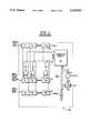
- FIG. 1shows a data correlator 100 which correlates serial input data to stored reference pattern data in real-time.
- the data correlator 100receives SERIAL INPUT DATA one bit at a time by serially shifting and latching the SERIAL INPUT DATA into data register 10.
- the serial shifting and latchingare enabled on the transition of a clock-1 signal (not shown).
- the SERIAL REFERENCE PATTERN DATAis clocked into a temporary reference data register (not shown) one bit at a time by serially shifting and latching on the transition of a clock-2 signal (not shown).
- the data in the temporary reference data registeris latched into reference data register 15 by a LATCH ENABLE signal (not shown).
- the data correlator 100receives serial mask data one bit at a time by serially shifting and latching the serial mask data into mask register 20.
- a threshold register 25is loaded 7 bits in parallel by an IO bus and latched by a CLOCK-3 (not shown).
- the hamming distance correlationis performed by the XOR-AND circuit 30.
- the XOR-AND circuit 30outputs a logic level 1 when a bit of data in the data register 10 is not the same logic value as the corresponding bit of data in the reference data register 15, excluding masked bit positions.
- a summation circuit 35sums all of the bits in agreement (e.g., when the hamming distance equal zero) received from the XOR-AND circuit 30, i.e all of the ones from the XOR-AND circuit 30 are added.
- the summation circuit 35either can output the sum directly to the 7 bit parallel bus IO or to a comparator 40.
- the comparator 40compares the summed value from the summation circuit 35 to a threshold value stored in threshold register 25.
- the comparator 40outputs a logic value 1 when the summed value is greater than or equal to the threshold value.
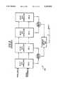
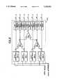
- FIG. 2shows a 128-bit data correlator 200 with four 32-bit data correlators 100 similar to the 64-bit data correlator shown in FIG. 1.
- the 32-bit data correlator 100is the same as 64-bit data correlator 100 except that the 32-bit data correlator 100 has 32 bit registers instead of 64-bit registers.
- serial input signals SERIAL DATA IN and SERIAL REFERENCE INare serially loaded as described for the 64-bit data correlator except the serial data flows from one 32-bit data correlator to the next adjacent correlator 100 until the correlator 100-3 stores the first thirty-two bits of the serial data.
- Each 32-bit data correlator 100outputs a correlation value as described for the 64-bit data correlator.
- the correlation valuesare summed two at a time by adders 210-0 and 201-1 and then combined in combining matrix 220.
- the combining matrix 220outputs the sum of the correlation values on a 8 bit parallel bus RESULTS.
- the data correlatorshave a predetermined word size, so a different chip is required when an application requires a different size word to be correlated.
- This limitationbecomes apparent when flexibility in word-length is needed: not only does it become costly to maintain a stock of several different word size chips but also the space required for the additional chips increases the size of the PC board to which the chips are mounted. Further, if the apparatus of FIG. 2 was to be used in a 32-bit configuration mode, correlators 100-1, 100-2 and 100-3 would be disabled, resulting in inefficient use of circuitry.
- a low-cost and efficient data correlatorwhich performs either auto-correlation or cross-correlation bit pattern comparisons between stored reference data and serial input data.
- the data correlator according to the present inventionhas selectable configurations responsive to external configuration signals.
- the data correlatorhas a 32-bit or 64-bit configuration
- the data correlatorperforms simultaneous correlations of a plurality of serial input data.
- the data correlatormay be configured internally as four 32-bit, two 64-bit or one 128-bit data correlator, whereby the four 32-bit or two 64-bit correlators operate in parallel.
- the internal configurationis transparent to the user once the internal configuration is chosen.
- each of the four 32 bit data correlatorsreceives 32 bits of serial input data from a corresponding serial input data line. Specifically, the leading bit of the input data is latched and the previously latched data is shifted. Thereafter, each 32 bit data correlator performs a 32-bit hamming distance correlation producing a correlation value.
- the correlatorsoperate in a pipelined mode, so that the latching shifting and correlating are performed within one clock cycle.
- the correlation valueis either passed to a threshold compare circuit to compare the correlation values to a predetermined threshold value or output directly to a microprocessor bus. If the correlation value is greater than the threshold value a low match flag is output.
- the match flags for each correlation valuesimultaneously appear on the microprocessor bus when a threshold compare operation is enabled. Bit positions which are not important to determine the correlation between data and reference data patterns can be masked out of the correlation when so designated by mask bits.
- the mask informationis loaded in 8-bit blocks through a 8 -bit microprocessor bus.
- the serial input datais loaded serially, and the reference data may be loaded either serially or parallely. Match flags and raw correlation results may be obtained for each correlation performed.
- two 32 bit correlatorswork in series, two sets of two 32 bit correlators each forming a 64-bit correlator.
- a data select circuitcontrols the pipeline-mode propagation of serial data throughout the 32-bit correlators. Specifically, two of the four 32 bit data correlators receive 64 bits of serial input data and the other two of the four 32-bit data correlators each receive the first 32 bits of serial input data after the data has passed through the first two 32-bit correlators and the data select circuit.
- Each 32 bit correlatorperforms a 32-bit hamming distance correlation at every clock cycle, producing a correlation value and carry-in bit.
- the correlation values of each set of two 32 bit correlatorare added together by a summation circuit to produce a 64-bit correlation value while preserving the carry-in bit.
- the correlation valueis either passed to a threshold compare circuit for comparison between the correlation values and the predetermined threshold value or output to a microprocessor bus. If the correlation value is greater than the threshold value a low match flag is output.
- the match flags for each correlation valueappears simultaneously on the microprocessor bus when a threshold compare operation is enabled.
- each of the carry-in bits of the 64-bit correlation valuesare preserved, the values can be combined to form a 128-bit correlation value.
- four 32 bit correlatorswork in series under the control of the data select circuit, resulting in one set of four 32 bit correlators working in conjunction.
- the first of the series of four 32 bit data correlatorslatches and shifts 128 serial bits, the next one latches and shifts 96 bits, the following one latches and shifts 64 bits, and the final one latches and shifts 32 bits of serial input data.
- Each 32 bit correlatorperforms a 32-bit hamming distance correlation after each latching and shifting of a bit, producing a correlation value during each clock cycle.
- the correlation values of each 32 bit correlatorare added together by the summation circuit to produce a 128-bit correlation value.
- the correlation valueis either passed to a threshold compare circuit for comparison between the correlation values and the predetermined threshold value or output to a microprocessor bus. If the correlation value is greater than the threshold value a low match flag is output. The match flag for the correlation value appears on the microprocessor bus when a threshold compare operation is enabled.
- the data correlatorincludes a CPU bus interface which enables the multiplexing of correlation scores and control instructions on the CPU microprocessor bus.
- the CPU bus interfacemultiplexes the appropriate data in response to a CPU address bus and a read/write signal from the microprocessor.
- the efficiency of the CPU busis enhanced by sharing data on the CPU bus, minimizing the number of data lines.
- the CPU bus interfacemultiplexes internal data on a single internal data bus to minimize data lines and maximize efficiency of the internal data bus.
- the data correlatoralso includes a control register which enables automatic addressing of the 32-bit correlators and the threshold registers.
- a control registerwhich enables automatic addressing of the 32-bit correlators and the threshold registers.
- the data correlatoralso includes a data select circuit which controls the propagation of serial data through the 32-bit comparators in accordance with the configuration mode of the data correlator.
- the data correlator according to the present inventioncan efficiently perform either as four 32-bit correlators operating simultaneously and in parallel, or two 64-bit correlators operating simultaneously and in parallel, or a single 128-bit correlator.
- the data correlatorincludes a summation circuit which effectively multiplexes the outputs of the 32-bit comparators in accordance with the configuration mode. Specifically, the summation circuit outputs either four 32-bit correlation results as 5-bit values, two 64-bit correlation results as 6-bit values, or a 128-bit correlation value as a 7-bit value. The summation circuit preserves the carry bit of the 32-bit correlation values to efficiently determine the 64-bit and 128-bit correlation values.
- the data correlator of the present inventionprovides a variable word-length correlator providing efficient and flexible correlation results.
- FIG. 1illustrates a block diagram of a conventional 64-bit digital data correlator.
- FIG. 2illustrates a block diagram of another conventional 128-bit digital data correlator.
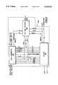
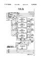
- FIG. 3shows a block diagram of a data correlator according to a preferred embodiment of the present invention.
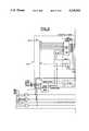
- FIG. 4shows an exemplary circuit diagram of the CPU bus interface of FIG. 3.
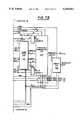
- FIG. 5shows an exemplary circuit diagram of the control unit of FIG. 3.
- FIG. 6shows a block diagram of the data comparator of FIG. 3.
- FIGS. 7A and 7Bshow an exemplary circuit diagram of the data comparator of FIG. 3.
- FIG. 8shows an exemplary circuit of the sum unit of FIG. 7B.
- FIG. 3shows a block diagram of a data correlator 350 according to a preferred embodiment of the present invention.
- the data correlator 350includes a CPU bus interface 330 for inputting and outputting data between the data correlator 350 and a conventional 8-bit microprocessor (CPU) bus.
- the CPU bushas an 8-bit parallel configuration, so that the CPU bus interface 330 outputs or receives the 8-bit data in parallel.
- the CPU bus interface 330can receive data such as control, reference, and mask data from the CPU bus. Also, the CPU bus interface 330 outputs correlation data such as correlation scores and match flags to the CPU bus.
- the CPU bus interface 330reads data off of the CPU bus when an externally-supplied read/write (R/W) control line is enabled. In the preferred embodiment of the present invention, a high signal on the R/W control line enables the CPU bus interface 330 to read the data on the CPU bus.
- the CPU bus interface 330also receives a least significant address bit ADX0 from an address bus to be used in conjunction with other control signals (described below) to control the output of the CPU bus interface 330 onto the CPU bus.
- the CPU bus interface 330is coupled to a data comparator 300 which outputs 8-bit correlation scores on a RESULT signal path and 4-bit match results (or match flags) on a MATCH OUT signal path indicating whether the correlation scores are within a corresponding threshold (described in detail below).
- the CPU bus interface 330outputs to the data comparator 300 correlation parameter data such as reference or mask data via an 8-bit signal path DI.
- the CPU bus interface 330also outputs control data to a control unit 310 via the 8-bit signal path DI.
- the CPU bus interface 330can transmit various control data and correlation parameter data on the single 8-bit DI signal path, thereby facilitating data transmission.
- the control unit 310receives read/write information from external circuitry through the read/write line (R/W) a described previously in reference to the CPU bus interface 300. Also, the control unit 310 receives address information from external circuitry via a 3-bit address but having address lines ADX0, ADX1, and ADX2.
- the control unit 310is coupled to the data comparator 300 and provides control data for loading and outputting data and configuration control data to determine the mode of operation by the data comparator 300.
- a 2-bit comparison out select signal COS output from control 310determines which match results are to be output by the data comparator 300 on the MATCH OUT signal path and output by the CPU bus interface 330.
- the control unit 310also outputs a write control line (READn) to enable the CPU gus interface 330 to output data so that external circuitry can read the data on the CPU bus.
- READnwrite control line
- the control unit 310receives internal configuration signals CI0 and CI1, which are externally-supplied and define the internal configuration of the data correlator 350, for example whether the data correlator 350 is to operate in a 32-bit, a 64-bit or a 128-bit mode.
- the configuration signals CI0 and CI1are decoded by the control unit 310 into four configurations of operation which are transmitted to the data comparator 300 and the CPU BUS interface 330 on control lines An, Bn, Cn and Dn.
- the control unit 310controls the correlation functions of the data comparator 300.
- the data comparator 300performs an exact match comparison in response to an exact match comparison signal EXACT MATCH COMP.
- the control unit 310also enables the proper loading of data on the DI signal path by the data comparator 300.
- loading of threshold information into data comparator 300is enabled by the 4-bit threshold load control line LD THRESH.
- the loading of mask information into data comparator 300 from the signal line DIis enabled by a 16-bit mask load control signal LD MASK from the control unit 310.
- the loading of correlator reference information into data correlator 300is enabled by a 16-bit reference load signal LD REF.
- the data comparator 300simultaneously receives via external circuitry four bits of serial input data through the 4-bit serial data stream SERIAL DATA IN and four bits of serial reference data through a 4-bit serial reference stream SERIAL REF IN.
- the data correlator 300can load correlation reference information either serially (via SERIAL REF IN) or in parallel (via DI) in response to the control unit 310.
- the manner in which the 4-bit serial input data streams SERIAL DATA IN and the 4-bit serial reference data streams SERIAL REF IN are utilized as input lineswill be explained in more detail in reference to FIGS. 7A and 7B.
- the data comparator 300simultaneously outputs to external circuitry four bits of serial data through 4-bit serial data streams SERIAL DATA OUT and four bits of serial reference data through 4-bit serial reference streams SERIAL REF OUT.
- the manner in which the 4-bit serial data streams SERIAL DATA OUT and serial reference data streams SERIAL REF OUT are utilized as output lineswill be explained in more detail in reference to FIGS. 7A and 7B.
- FIG. 4shows an exemplary circuit diagram of the CPU BUS interface 330 shown in FIG. 3.
- the READn signalcontrols a tri-state buffer 435 to enable the transmission of signals EXOUT to a pad pin 440 and an electrode 445 to direct the signal EXOUT onto the CPU bus.
- the signal EXOUTis an inverted output of an array of 2-to-1 multiplexers 420, which output either an 8-bit RESULT signal or a MATCH OUT signal in response to the ADX address signal and the Dn configuration signal.
- multiplexer 420-0outputs the MATCH OUT(3) signal
- the Dn signaldefines a predetermined configuration state, such as a special chip-compatability mode.
- the CPU bus interface 330inputs data from the CPU bus as shown in FIG. 4. An input signal is transmitted to the electrode 445 and pad pin 440 and then latched by an input buffer 415 in response to a read/write signal R/W.
- FIG. 5shows an exemplary circuit diagram of the control unit 310 shown in FIG. 3.
- the internal configuration signals CI0 and CI1are decoded to provide control signals An, Bn, Cn and Dn.
- the internal configuration signals CI0 and CI1are used to select the mode of operation for the data correlator 350.
- the data correlator 350operates internally as four 32-bit correlators when CI0 and CI1 are both logic level zero (mode A).
- mode Blogic level one
- mode Btwo 64-bit data correlators
- the data correlator 350operates as one 128-bit data correlator when internal configuration signal CI1 is a logic level 1 (mode C & D).
- the data correlator 350operates in a CS1212 chip compatible mode when both internal configuration signals CI0 & CI1 are logic level 1 (mode D).
- the CS1212 chip compatabilityis a protocol used with the CS1212 chip disclosed by Chip Supply, Inc., Orlando Fla. The available configuration options are summarized in TABLE 1.
- Reading and writing data in the data correlator 350is controlled by an address decoder 505.
- the address decoder 505decodes address signals ADX0, ADX1, and ADX2, mode signals An, Bn and Dn and the read/write signal R/W to output control signals WRITE CONT, WRITE DATA, READn and the comparison out select signal COS.
- Table 2shows the functions performed in response to the inputs to the address decoder 505.
- the data to be written to the data comparator 350is addressed by a control register 510.
- the control register 510performs automatic addressing of the data to be written to the data comparator 300.
- the automatic addressingis performed by incrementing the address input via the DI signal line to the control register 510.
- the control register 510automatically determines the appropriate address for the subsequent data supplied on the 8-bit data DI bus.
- TABLE 3shows the configuration of the control register 510.
- the data bits 0-3 on the DI buscorrespond to address signals A0-A3 for addressing up to sixteen register locations.
- the data bits DI(4) and DI(5)correspond to register select signals S0 and S1, respectively.
- Data bit DI(6)enables the autoincrement signal AINC
- data bit DI(7)enables the exact match comparator EMC signal (described in further detail with reference to FIGS. 7A and 7B).
- the control register 510includes a counter 515, and two D flip-flops 520 and 525.
- the write control signal WRITE CONT from the address decoder 505enables the control register 510.
- D flip flop 525latches control signal EXACT MATCH COMP (EMC) from the data input bus DI(7), which determines if an exact match comparison is to be performed.
- D flip flop 520latches an autoincrement signal AINC from data input bus DI(6) in response to the write control register enable signal WRITE CONT from the decoder 505.
- the counter 515is a modulo 128 counter which latches the address input by bits 0-5 of the DI signal line. The counter 515 automatically increments to a next sequential address in response to the automatic increment signal AINC output by D flip flop 520, and outputs address lines A0-A3, S0 and S1.
- the register select signals S0 and S1are output from the counter 515 of the control register 510 to a decoder 530, which outputs an enable signal in response to the register select signals.
- the threshold decoder 545outputs the 4-bit threshold register load signals LD THRESH in response to the internal configuration signals An and Bn and address signals A0 and A1.
- the reference decoder 540 and the mask decoder 535output a 16-bit reference register load signal LD REF and a 16-bit mask register load control signal LD MASK in response to the address signals A0-A3, respectively.
- FIG. 6shows a block diagram of the data comparator 300 according to the preferred embodiment of the present invention.
- Each correlator 400performs a 32-bit hamming distance comparison between input data and a reference data and outputs a 5-bit correlation value.
- the 5-bit correlation valueis input to a 5-bit threshold unit 430 if the data comparator 300 is configured internally as four 32-bit correlators. There are four 5-bit threshold units 430, one for each 32-bit correlator 400.
- the 5-bit correlation valueis passed to a 6-bit summation unit 420 if the data comparator 300 is configured internally as two 64-bit correlators. There are two 6-bit summation units 620, each one for two 32-bit correlators.
- correlator 400-0 and correlator 400-1output their respective 5-bit correlation values to summation unit 420-1.
- Correlator 400-2 and correlator 400-3output their respective 5-bit correlation values to summation unit 420-2.
- Each 6-bit summation unit 420-1 and 420-2outputs a 6-bit summation output to a 6-bit threshold unit 440-0 and 440-1, respectively.
- each 6-bit summation unitoutputs its 6-bit value to a 7-bit summation unit 460 for use when the data comparator 300 is configured internally as one 128-bit correlator.
- the 7-bit summation unitpasses its 7-bit summation output to a 7-bit threshold unit 450.
- FIGS. 7A and 7Bshow an exemplary circuit diagram of the data comparator 300 shown in FIGS. 3 and 6.
- FIG. 7Ais a first half of the data comparator 300 circuit diagram
- FIG. 7Bis a second half of the data comparator circuit diagram, so that the two figures should be considered together.
- four 32-bit comparators 705are each coupled to the DI bus and the serial load register control signal SLR.
- each 32-bit comparator 705receives four bits of the 16-bit LD MASK and LD REF signals, respectively, such that comparator 705-0 receives bits 0-3, comparator 705-1 receives bits 4-7, comparator 705-3 receives bits 8-11 and comparator 705-2 receives bits 12-15.
- the data correlator 300also includes a data select circuit 710 which receives simultaneous four bit input serial data streams (SERIAL DATA IN) and the simultaneous four bit input serial reference data streams (SERIAL REF IN).
- the data select unit 710outputs the SERIAL DATA IN on the 4-bit DIN signal path and the SERIAL REF IN on the 4-bit RIN signal path to the 32-bit comparators 705 in response to the mode signals An and Cn.
- the comparators 705-0, 705-1, 705-3 and 705-2receive bits 0, 1, 2 and 3 of the DIN and RIN signal paths, respectively.
- the comparators 705-0, 705-1, 705-3 and 705-2output bits 0, 1, 2 and 3 of a SDAT and SREF signal path to the data select circuit 710, respectively.
- the comparators 705 and the data select circuit 710are synchronized by a clock signal (not shown) in order to latch the serial data. Specifically, each comparator latches the leading bit on the DIN signal line and shifts the data currently-stored data (for example, the previously-latched data) in response to the clock signal (not shown). Thereafter, each comparator performs a 32-bit hamming distance correlation. Thus, each of the comparators 705 operate in a pipelined mode, so that the latching shifting and correlating is performed within each clock cycle.
- the data select circuit 710directs one of two input serial data streams along signal path DIN to the 32-bit compare unit 705-0 and 705-2; the 32-bit comparators 705-0 and 705-2 serially shift the input serial data stream and output the serial data stream on signal paths SDAT(0) and SDAT(3) until 64 bits have been input to the comparators 705-0 and 705-2.
- the data select unit 710sequentially receives the first 32 bits of the two data streams from the signal path SDAT and passes them in sequential lock step fashion (e.g., serial shift and latch) to the next 32-bit comparators 705-1 and 705-3, respectively, to effectively create a 64-bit comparator.
- the 32-bit compare unit 705-0passes the first 32-bits to 32-bit compare unit 705-1, so that the 32-bit comparator 705-0 stores the upper half of a 64-bit word and the 32-bit comparator 705-1 stores the lower half of the 64-bit word.
- the comparator 705-2passes the first thirty-two bits of the 64-bit word through the data select unit 710 to the 32-bit comparator 705-3.
- the data select circuit 710sequentially routes only one of the input serial data streams (e.g., bit 0 of SERIAL DATA IN) through all four 32-bit comparators 705-0, 705-1, 705-2 and 705-3 in lock step fashion to obtain the 128 bits of comparison.
- the first serial bit for the 128-bit data streamwill follow the signal path: SERIAL DATA IN(0), DIN(0), SDAT(0), DIN(1), SDAT(1), DIN(3), SDAT(3), DIN(2).
- the first serial bit for the 128-bit data streamwill ultimately be stored in the 32-bit comparator 705-3, while the 128-th serial bit will be stored in the 32-bit comparator 705-0.
- the input serial reference data (SERIAL REF IN) signalsare handled in the same manner as the input serial data (SERIAL DATA IN) when a serially load reference data signal (SLR) enables the 32-bit comparators 705.
- SLRserially load reference data signal
- the comparators 705latch the serial reference data in response to the serial load reference data signal SLR; otherwise, the reference data may be loaded in parallel from the DI bus, as explained below.
- the 32-bit comparators 705may be parallely loaded with reference data presented on the 8-bit data lines DI in response to the serial load reference control signal SLR.
- Each 32-bit comparatorreceives a 4-bit LD REF signal: each bit of the 4-bit LD REF signal corresponds to an 8-bit-wide data slice within the 32-bit comparator.
- reference datais segmented into 8-bit contiguous slices (i.e. 0-7, 8-15, 16-23, 24-31); each of these slices latch the data on the 8-bit DI bus in response to the corresponding bit of the 4-bit LD REF signal.
- the mask datais loaded in parallel fashion only.
- the 8-bit parallel data input line DIloads the 32-bit comparator 705 in 8-bit slices in response to the corresponding LD MASK bit in the same manner as described above for the parallel loading of the reference data.
- a 4-bit mask load control signal LD MASKis input to each 32-bit comparator 705 as shown in FIG. 7, i.e. the lowest four bits LD MASK(0-3) are input to 32-bit comparator 705-0, bits LD MASK(4-7) are input to 32-bit comparator 705-1, bits LD MASK(8-11) are input to the 32-bit comparator 705-3, and bits LD MASK(12-15) are input to the 32-bit comparator 705-2.
- the reference data input to the 32-bit comparator 705(either by serially loading RIN or parallely loading DI) is stored in a reference data register within the 32-bit comparator 705.
- Each 32-bit comparator 705also includes a data register for storing input serial data, and a mask data register for storing input mask data.
- the correlation process within each of the 32-bit comparators 705will now be described.
- the stored input datais bitwise exclusively nor'd (e.g., XOR function has an inverted output) with the stored reference data and bitwise AND'd with the stored mask data producing a hamming correlation between the stored data and the stored reference data.
- An exact match signal EMis output high from the comparator 705 when an exact match is found (e.g., the hamming distance equals zero) between the stored input data and the stored reference data.
- the number of bit matches in the hamming correlationare summed and output from each 32-bit comparator 705-0, 705-1, 705-2, 705-3 on 5-bit signal lines A1, B1, A2 and B2 respectively.
- the 5-bit signalrepresents up to 32 possible outcomes in the comparison (i.e., there could be 32 matches in a 32-bit comparison).
- the 32-bit comparators 705-0, 705-1, 705-2 and 705-3each output an expansion bit signal A1+1, B1+1, A2+1 and B2+1 respectively, which represent a carry in bit for subsequent summations if the 64-bit or 128-bit comparator configuration is selected.
- Each 32-bit comparator 705outputs serial reference data SREF and serial data SDAT, which is output to the data select circuit 710 and external circuitry (not shown).
- the comparison results of the 32-bit comparators 705 and the corresponding expansion bit signals (carry-in bits)are input to a summation circuit 715.
- the summation circuit 715collects the 32-bit comparison results and selectively integrates the results into two 64-bit correlation results or one 128-bit correlation result in response to the internal configuration mode control signals An and Cn. Specifically, if the data comparator 300 is operating in the four 32-bit correlator mode, the summation circuit 715 passes the results of the 32-bit comparators 705 (A1, B1, B1+1, A2, A2+1, B2 and B2+1) to a threshold compare circuit 720.
- the summation circuit 715functions in a manner similar to the summation circuit 420 shown in FIG. 6; the summation circuit 715 adds the results A1 and B1 of the 32-bit comparators 705-0 and 705-1 (and carry signal B1+1), and also adds the results A2 and B2 of the comparators 705-2 and 705-3 (and carry signal B2+1) and outputs the two 64-bit correlation results as 6-bit values on the S1 and S2 signal lines.
- the summation circuit 715functions in a manner similar to the summation circuit 460 shown in FIG. 6; the summation circuit 715 adds the 64-bit results calculated above and includes the carry signal A2+1, and outputs the 128-bit correlation results as a 7-bit value on the S1 signal line.
- carry in bits B1+1, A2+1 and B2+1 from 32-bit comparator 705-1, 705-2, and 705-3are all used by summation circuit 715 to compensate for the different modes of operation (to be described in more detail in reference to FIG. 8).
- the results of summation circuit 715are output to the threshold compare circuit 720 through a logic circuit 725 to make corrections due to the mode of operation.
- logic circuit 725-0allows the results of 32-bit comparator 705-0 (Al and A1+1) to pass through to threshold compare circuit 720 through signal lines ALI and CARRY0 respectively when the 32-bit data correlation mode is chosen.
- the logic circuit 725-1works in the same manner as logic circuit 725-0 except it works in conjunction with 32-bit comparator 705-2, so that input signals A2 and A2+1 are passed through to the threshold compare circuit 720 through signal lines AL2 and CARRY2, respectively.
- the logic circuits 725are arranged to inhibit propagation of data to the threshold compare circuit 720 when any mode other than the 32-bit data correlation mode is selected.
- the threshold compare circuit 720is loaded with threshold data (e.g., the predetermined value for a threshold test) through the 8-bit parallel data input bus DI.
- the threshold data from the 8-bit parallel data input bus DIis latched in a threshold register within threshold compare circuit 720 in response to the 4-bit LD THRESH signal.
- Bit DI(0)is the least significant bit from the data bus DI and bits DI(4), DI(5) and DI(6) are the most significant bits for the 32-bit, 64-bit and 128-bit modes, respectively.
- TABLE 4shows the magnitude of the bits written to the threshold register within threshold compare circuit 720.
- the parallel data DIis latched in by the 4-bit threshold load control signal LD THRESH.
- Each bit of the LD THRESH signalcontrols one of the four threshold registers, so that each of the four threshold registers may store a separate threshold value when the data correlator is operated in the 4 ⁇ 32-bit mode. Similarly, only two threshold registers are needed when the data correlator is operated in the 2 ⁇ 64-bit mode.
- the internal configuration mode control signals An, Cn and Dnare input to threshold compare circuit 720 to determine the size of comparison to be performed and whether to operate in the CS1212 compatible mode.
- the correlation result from the correlatorse.g., the number of bits of the input data which are different from the reference data
- the threshold compare circuit 720also outputs the results of a threshold comparison operation on signal path MATCH, indicating whether the sum of correlated bits in agreement are less than or equal to the threshold data value.
- Four parallel bit lines MATCH(0) to MATCH(3)are output from the threshold compare circuit 720 when the 32-bit correlation mode is selected.
- the threshold compare circuit 720outputs two parallel data lines MATCH(0) and MATCH(1) when the 64-bit data correlation mode is selected.
- One data line MATCH(0)is output by threshold compare circuit 720 when the 128-bit data correlation mode is selected.
- the exact match comparison control signal(EXACT MATCH COMP/EMC) enables a match circuit 730 to determine if an exact match has been made between the reference data and the input data.
- the match circuit 730either combines the exact match signals (EM) from 32-bit comparator 705 or else passes the results of the exact match signal (EM) of the 32-bit comparator 705 directly through to four parallel lines MATCH OUT, depending on which mode of operation has been selected.
- Internal configuration mode control signals An and Bnare used to determine which mode of operation has been selected by match circuit 730.
- the match circuit 730outputs the results of an exact match comparison onto four parallel data bit streams MATCH OUT(0) to MATCH OUT(3) if the 32 bit comparator mode has been selected.
- Two parallel data bit lines MATCH OUT(0) and MATCH OUT(1)are output by the match circuit 730 when the 64-bit data comparator mode is selected.
- the match circuit 730outputs one data bit line MATCH OUT(0) when the 128-bit data correlator mode is selected.
- the match circuit 730will output the final results of a threshold comparison from the threshold comparator circuit 720 when the exact match compare control signal (EMC) is inverted.
- EMCexact match compare control signal
- Four parallel data lines MATCH OUT(0) to MATCH OUT(3)are used when the 32-bit data correlator mode is selected.
- Two data lines MATCH OUT(0) and MATCH OUT(1)are used when the 64-bit correlation mode is selected, and one data line MATCH OUT(0) is used when the 128-bit data correlator mode is selected.
- the match circuit 730can output either the results of an exact match comparison or the results of the threshold comparison in response to the EMC signal.
- FIG. 8shows an exemplary circuit diagram of summation circuit 715 shown in FIG. 7.
- the summation circuit 715includes a primary 64-bit adder 840, a secondary 64-bit adder 845, and a 128-bit adder 835.
- the primary and secondary adders 840 and 845each add the 32-bit correlation results in order to obtain a 64-bit correlation result and the 128-bit adder 835 adds the results of the 64-bit adders 840 and 845 to obtain the 128-bit correlation result.
- the adders 840, 845 and 835are enabled in response to the internal configuration mode of the data correlator.
- 128-bit adder 835 and 64-bit adders 840 and 845are enabled when the data correlator is in the 128-bit configuration.
- the 128-bit adderis disabled via the configuration mode signal Cn so that the output signal ADD RESULT from the secondary 64-bit adder 845 is passed through the adder 835.
- the 64-bit adders 840 and 845are disabled by the configuration signal An, the 32-bit correlation result signals B1 and B2 are passed through the respective adders so that signal B1 is passed to the lowest five bits of output signal S2 and signal B1 is passed to the lowest five bits of output signal S1.
- the operation of the summation circuit 715will be described in more detail below.
- the internal configuration mode signal Anis logically AND'd with carry in signal B1+1 in AND gate 825-0.
- the result of AND 825-0is a 1 when both B1+1 and An are both a logic 1.
- the result of AND 825-0is fed to a carry in input of a full adder 815-0.
- the addition of this carry in bitallows the expansion of the effective correlator word length to 64-bits from two 32-bit comparators 705.
- the internal configuration signal Anis AND'd in AND gates 825 with the results of 32-bit comparator 705-0 (A1) to allow either the pass through of result signal of 32-bit comparator 705-1 or B1 on the addition of signals A1 and B1 in full adders 815.
- the AND gate 825will output zero to full adders 815.
- the addition of zero to result of 32-bit comparator 205-1 on signal B1passes the result B1 directly through full adders 815, effectively creating a pass through of signal B1.
- Full adders 820 and AND gates 830work in the same manner except result A2 is substituted for result A1, result signal B2 is substituted for result signal B1, and carry signal B2+1 is substituted for carry signal A2+1.
- the operation of the 128-bit adder 835is similar to the operation of the 64-bit adders 840 and 845.
- the carry in signal A2+1is logically AND'd with internal configuration mode control signal Cn in AND gate 805-0 when carry in bit A2+1 from 32-bit comparator 705-2 is a logic level 1 and internal configuration mode control signal Cn is a logic 1 (128-bit correlation mode selected).
- the AND gate 805-0sends the carry in bit A2+1 to a carry input of full adder 810-0 allowing for the increased magnitude required to sum 128 bits from the six-bit signals ADD RESULT and S2 from the adders 845 and 840, respectively.
- the addition resultis output as a 7-bit value on the signal path S1, which represents the 7-bit correlation value for the 128-bit correlation.
- the summation circuit 715is capable of performing multiple addition processes in order to obtain the appropriate bit-length comparison result. Since the carry-in values are preserved for the 32-bit and 64-bit correlation values, the 128-bit result can be quickly determined by one extra addition process.
- the present inventionenables a user to select the word length of a hamming data correlator with ease and minimal addressing modifications.
- a usercan configure the data correlator to perform in a 4 ⁇ 32-bit mode, a 2 ⁇ 64-bit mode or a 128-bit mode.
- the 32-bit data correlatorsreceive data from a data select circuit which transmits serial data in accordance with the selected configuration of the data correlator. Data is efficiently transmitted on the CPU data bus, namely the CPU data bus shares correlation results from the data correlator with control instructions from the microprocessor. As a result, efficiency of data manipulation between the external microprocessor and the data correlator is improved.
- the preferred embodimentuses 32-bit, 64-bit and 128-bit length correlators, it will be appreciated that any length correlator can be used, either by masking out a portion of the correlators, or by using a different base-length correlator other than 32 bits. Also, one skilled in the art will appreciate that a plurality of data correlators may be coupled to increase the capacity of bit-length or parallel correlations. Further, the preferred embodiment may be modified by having an internal memory, such as a RAM or mask ROM to store control data, reference data or mask data.
- an internal memorysuch as a RAM or mask ROM to store control data, reference data or mask data.
- results of data correlationcould be output to an internal memory for future comparisons.
- the reference valuecould be updated in accordance with the determined correlation result RESULT so that an adaptive correlation could be realized.
Landscapes
- Engineering & Computer Science (AREA)
- Physics & Mathematics (AREA)
- General Physics & Mathematics (AREA)
- Mathematical Physics (AREA)
- Computational Mathematics (AREA)
- Theoretical Computer Science (AREA)
- Mathematical Analysis (AREA)
- Mathematical Optimization (AREA)
- Pure & Applied Mathematics (AREA)
- Data Mining & Analysis (AREA)
- Algebra (AREA)
- Databases & Information Systems (AREA)
- Software Systems (AREA)
- General Engineering & Computer Science (AREA)
- Computing Systems (AREA)
- Synchronisation In Digital Transmission Systems (AREA)
Abstract
Description
TABLE 1 ______________________________________ Configuration Options: C0 C1 Correlator Configuration ______________________________________ 0 0 4 × 32 bit correlator (Mode A) 1 0 2 × 64 bit correlator (Mode B) 0 1 1 × 128 bit correlator (Mode C) 1 1 1 × 128 bit correlator (Mode D) (CS1212 compatible) ______________________________________
TABLE 2 ______________________________________ FUNCTIONS OF DATA CORRELATOR ADX2 ADX1 ADx0 Data Correlator Function ______________________________________ 0 0 0Output comparator 0results 0 0 1Output comparator 1results 0 1 0Output comparator 2results 0 1 1Output comparator 3results 1 0 0 Read control information into control register (Modes A, B & C) 1 0 1 Read data register selected (Modes A,B,C) 1 1 0 Read control register selected (Mode D) 1 1 1 Access data register selected (Mode ______________________________________ D) * = Don't care
TABLE 3 ______________________________________ D7 D6 D5 D4 D3 D2 D1 bit positions ______________________________________ EMC AINC S1-S0 A3-A0 signal ______________________________________
TABLE 4 ______________________________________ Threshold Register (S1 - 0 = 11): D7 D6 D5 D4 D3 D2 D1 D0 ______________________________________ MSB LSB MSB LSB MSB LSB BIT4 BIT5 BIT6 MSB BIT3 BIT2 BIT1 LSB ______________________________________
Claims (10)
Priority Applications (1)
| Application Number | Priority Date | Filing Date | Title |
|---|---|---|---|
| US07/767,330US5218562A (en) | 1991-09-30 | 1991-09-30 | Hamming data correlator having selectable word-length |
Applications Claiming Priority (1)
| Application Number | Priority Date | Filing Date | Title |
|---|---|---|---|
| US07/767,330US5218562A (en) | 1991-09-30 | 1991-09-30 | Hamming data correlator having selectable word-length |
Publications (1)
| Publication Number | Publication Date |
|---|---|
| US5218562Atrue US5218562A (en) | 1993-06-08 |
Family
ID=25079152
Family Applications (1)
| Application Number | Title | Priority Date | Filing Date |
|---|---|---|---|
| US07/767,330Expired - LifetimeUS5218562A (en) | 1991-09-30 | 1991-09-30 | Hamming data correlator having selectable word-length |
Country Status (1)
| Country | Link |
|---|---|
| US (1) | US5218562A (en) |
Cited By (54)
| Publication number | Priority date | Publication date | Assignee | Title |
|---|---|---|---|---|
| US5463645A (en)* | 1992-06-19 | 1995-10-31 | Nec Corporation | System for detecting non-coincidence of codes |
| US5517518A (en)* | 1994-07-21 | 1996-05-14 | Digital Security Controls Ltd. | Method and arrangement for recognition of a coded transmitted signal |
| US5535402A (en)* | 1992-04-30 | 1996-07-09 | The United States Of America As Represented By The Secretary Of The Navy | System for (N•M)-bit correlation using N M-bit correlators |
| US5646628A (en)* | 1994-12-09 | 1997-07-08 | Telefonaktiebolaget Lm Ericsson | Method of treating periodic signals |
| US5666550A (en)* | 1995-06-07 | 1997-09-09 | International Business Machines Corporation | Bus operation circuit using CMOS ratio logic circuits |
| US5684727A (en)* | 1996-02-07 | 1997-11-04 | Macdonald, Dettwiler And Associates Ltd. | High-speed correlator |
| US5822365A (en)* | 1995-12-30 | 1998-10-13 | Samsung Electronics Co., Ltd. | Variable correlator |
| US5951711A (en)* | 1993-12-30 | 1999-09-14 | Texas Instruments Incorporated | Method and device for determining hamming distance between two multi-bit digital words |
| US20010005403A1 (en)* | 1999-12-27 | 2001-06-28 | Hyundai Electronics Industries Co., Ltd. | Apparatus for calculating decision parameters in an IMT-2000 system |
| US6330702B1 (en)* | 1997-12-19 | 2001-12-11 | Bae Systems Plc | Hamming value determination and comparison |
| US20030103581A1 (en)* | 2001-11-09 | 2003-06-05 | Rawlins Gregory S. | Method and apparatus for reducing DC offsets in a communication system |
| US20030128776A1 (en)* | 2001-11-09 | 2003-07-10 | Parkervision, Inc | Method and apparatus for reducing DC off sets in a communication system |
| US20030181186A1 (en)* | 1999-04-16 | 2003-09-25 | Sorrells David F. | Reducing DC offsets using spectral spreading |
| US20030224752A1 (en)* | 2002-06-04 | 2003-12-04 | Parkervision, Inc. | Method and apparatus for DC offset removal in a radio frequency communication channel |
| US20030227983A1 (en)* | 2002-06-07 | 2003-12-11 | Parkervision, Inc. | Active polyphase inverter filter for quadrature signal generation |
| US20030229636A1 (en)* | 2002-06-06 | 2003-12-11 | Mattausch Hans Juergen | Pattern matching and pattern recognition system, associative memory apparatus, and pattern matching and pattern recognition processing method |
| US6748015B2 (en)* | 1996-04-25 | 2004-06-08 | Sirf Technology, Inc. | Spread spectrum receiver with multi-bit correlator |
| US6853690B1 (en) | 1999-04-16 | 2005-02-08 | Parkervision, Inc. | Method, system and apparatus for balanced frequency up-conversion of a baseband signal and 4-phase receiver and transceiver embodiments |
| US20050049984A1 (en)* | 1997-12-19 | 2005-03-03 | Bae Systems Plc | Neural networks and neural memory |
| US20060019617A1 (en)* | 2000-04-14 | 2006-01-26 | Parkervision, Inc. | Apparatus, system, and method for down converting and up converting electromagnetic signals |
| US7006805B1 (en) | 1999-01-22 | 2006-02-28 | Parker Vision, Inc. | Aliasing communication system with multi-mode and multi-band functionality and embodiments thereof, such as the family radio service |
| US7010559B2 (en)* | 2000-11-14 | 2006-03-07 | Parkervision, Inc. | Method and apparatus for a parallel correlator and applications thereof |
| US7016663B2 (en) | 1998-10-21 | 2006-03-21 | Parkervision, Inc. | Applications of universal frequency translation |
| US7027786B1 (en) | 1998-10-21 | 2006-04-11 | Parkervision, Inc. | Carrier and clock recovery using universal frequency translation |
| US7050508B2 (en) | 1998-10-21 | 2006-05-23 | Parkervision, Inc. | Method and system for frequency up-conversion with a variety of transmitter configurations |
| US7054296B1 (en) | 1999-08-04 | 2006-05-30 | Parkervision, Inc. | Wireless local area network (WLAN) technology and applications including techniques of universal frequency translation |
| US7065162B1 (en) | 1999-04-16 | 2006-06-20 | Parkervision, Inc. | Method and system for down-converting an electromagnetic signal, and transforms for same |
| US7072390B1 (en) | 1999-08-04 | 2006-07-04 | Parkervision, Inc. | Wireless local area network (WLAN) using universal frequency translation technology including multi-phase embodiments |
| US7076011B2 (en) | 1998-10-21 | 2006-07-11 | Parkervision, Inc. | Integrated frequency translation and selectivity |
| US7082171B1 (en) | 1999-11-24 | 2006-07-25 | Parkervision, Inc. | Phase shifting applications of universal frequency translation |
| US7110444B1 (en) | 1999-08-04 | 2006-09-19 | Parkervision, Inc. | Wireless local area network (WLAN) using universal frequency translation technology including multi-phase embodiments and circuit implementations |
| US7110435B1 (en) | 1999-03-15 | 2006-09-19 | Parkervision, Inc. | Spread spectrum applications of universal frequency translation |
| US7194246B2 (en) | 1998-10-21 | 2007-03-20 | Parkervision, Inc. | Methods and systems for down-converting a signal using a complementary transistor structure |
| US7209725B1 (en) | 1999-01-22 | 2007-04-24 | Parkervision, Inc | Analog zero if FM decoder and embodiments thereof, such as the family radio service |
| US7236754B2 (en) | 1999-08-23 | 2007-06-26 | Parkervision, Inc. | Method and system for frequency up-conversion |
| US7245886B2 (en) | 1998-10-21 | 2007-07-17 | Parkervision, Inc. | Method and system for frequency up-conversion with modulation embodiments |
| US20070206709A1 (en)* | 2006-03-03 | 2007-09-06 | Pmc-Sierra Israel Ltd. | Enhancing the ethernet FEC state machine to strengthen correlator performance |
| US7292835B2 (en) | 2000-01-28 | 2007-11-06 | Parkervision, Inc. | Wireless and wired cable modem applications of universal frequency translation technology |
| US7295826B1 (en) | 1998-10-21 | 2007-11-13 | Parkervision, Inc. | Integrated frequency translation and selectivity with gain control functionality, and applications thereof |
| US7308242B2 (en) | 1998-10-21 | 2007-12-11 | Parkervision, Inc. | Method and system for down-converting and up-converting an electromagnetic signal, and transforms for same |
| US7379883B2 (en) | 2002-07-18 | 2008-05-27 | Parkervision, Inc. | Networking methods and systems |
| US7454453B2 (en) | 2000-11-14 | 2008-11-18 | Parkervision, Inc. | Methods, systems, and computer program products for parallel correlation and applications thereof |
| US7460584B2 (en) | 2002-07-18 | 2008-12-02 | Parkervision, Inc. | Networking methods and systems |
| US7483686B2 (en) | 1999-03-03 | 2009-01-27 | Parkervision, Inc. | Universal platform module and methods and apparatuses relating thereto enabled by universal frequency translation technology |
| US7515896B1 (en) | 1998-10-21 | 2009-04-07 | Parkervision, Inc. | Method and system for down-converting an electromagnetic signal, and transforms for same, and aperture relationships |
| US7554508B2 (en) | 2000-06-09 | 2009-06-30 | Parker Vision, Inc. | Phased array antenna applications on universal frequency translation |
| US20100005254A1 (en)* | 2008-07-02 | 2010-01-07 | Cooke Laurence H | Nearest Neighbor Serial Content Addressable Memory |
| US7693230B2 (en) | 1999-04-16 | 2010-04-06 | Parkervision, Inc. | Apparatus and method of differential IQ frequency up-conversion |
| EP2280290A1 (en)* | 2009-07-10 | 2011-02-02 | FCS Flight Calibration Services GmbH | Secondary signal receiver and method for determining defined receiver times of secondary radar signals in a multilateration system |
| US8279546B1 (en)* | 2006-06-07 | 2012-10-02 | Marvell International Ltd. | Systems and methods for sync mark detection using correlation |
| US8295406B1 (en) | 1999-08-04 | 2012-10-23 | Parkervision, Inc. | Universal platform module for a plurality of communication protocols |
| US8976477B1 (en)* | 2014-02-12 | 2015-03-10 | Lsi Corporation | System and method for generating soft-orthogonal syncmarks |
| US9129042B2 (en) | 2008-07-02 | 2015-09-08 | Laurence H. Cooke | Nearest neighbor serial content addressable memory |
| US9197304B2 (en) | 2008-02-04 | 2015-11-24 | Nokia Technologies Oy | Method and apparatus for conveying antenna configuration information via masking |
Citations (3)
| Publication number | Priority date | Publication date | Assignee | Title |
|---|---|---|---|---|
| US4559607A (en)* | 1983-07-11 | 1985-12-17 | International Telephone And Telegraph Corporation | Arrangement to provide an accurate time-of-arrival indication for a plurality of received signals |
| US4825401A (en)* | 1986-03-31 | 1989-04-25 | Kabushiki Kaisha Toshiba | Functional dividable multiplier array circuit for multiplication of full words or simultaneous multiplication of two half words |
| US4933952A (en)* | 1988-04-08 | 1990-06-12 | Lmt Radioprofessionnelle | Asynchronous digital correlator and demodulators including a correlator of this type |
- 1991
- 1991-09-30USUS07/767,330patent/US5218562A/ennot_activeExpired - Lifetime
Patent Citations (3)
| Publication number | Priority date | Publication date | Assignee | Title |
|---|---|---|---|---|
| US4559607A (en)* | 1983-07-11 | 1985-12-17 | International Telephone And Telegraph Corporation | Arrangement to provide an accurate time-of-arrival indication for a plurality of received signals |
| US4825401A (en)* | 1986-03-31 | 1989-04-25 | Kabushiki Kaisha Toshiba | Functional dividable multiplier array circuit for multiplication of full words or simultaneous multiplication of two half words |
| US4933952A (en)* | 1988-04-08 | 1990-06-12 | Lmt Radioprofessionnelle | Asynchronous digital correlator and demodulators including a correlator of this type |
Cited By (120)
| Publication number | Priority date | Publication date | Assignee | Title |
|---|---|---|---|---|
| US5535402A (en)* | 1992-04-30 | 1996-07-09 | The United States Of America As Represented By The Secretary Of The Navy | System for (N•M)-bit correlation using N M-bit correlators |
| US5463645A (en)* | 1992-06-19 | 1995-10-31 | Nec Corporation | System for detecting non-coincidence of codes |
| US5951711A (en)* | 1993-12-30 | 1999-09-14 | Texas Instruments Incorporated | Method and device for determining hamming distance between two multi-bit digital words |
| US5517518A (en)* | 1994-07-21 | 1996-05-14 | Digital Security Controls Ltd. | Method and arrangement for recognition of a coded transmitted signal |
| US5646628A (en)* | 1994-12-09 | 1997-07-08 | Telefonaktiebolaget Lm Ericsson | Method of treating periodic signals |
| US5758179A (en)* | 1995-06-07 | 1998-05-26 | International Business Machines Corporation | Bus operation circuit using CMOS ratio logic circuits |
| US5666550A (en)* | 1995-06-07 | 1997-09-09 | International Business Machines Corporation | Bus operation circuit using CMOS ratio logic circuits |
| US5822365A (en)* | 1995-12-30 | 1998-10-13 | Samsung Electronics Co., Ltd. | Variable correlator |
| US5684727A (en)* | 1996-02-07 | 1997-11-04 | Macdonald, Dettwiler And Associates Ltd. | High-speed correlator |
| US6748015B2 (en)* | 1996-04-25 | 2004-06-08 | Sirf Technology, Inc. | Spread spectrum receiver with multi-bit correlator |
| US7729413B2 (en)* | 1996-04-25 | 2010-06-01 | Sirf Technology, Inc. | Spread spectrum receiver with multi-bit correlator |
| US20040202235A1 (en)* | 1996-04-25 | 2004-10-14 | Sanjai Kohli | Spread spectrum receiver with multi-bit correlator |
| US6330702B1 (en)* | 1997-12-19 | 2001-12-11 | Bae Systems Plc | Hamming value determination and comparison |
| US20050049984A1 (en)* | 1997-12-19 | 2005-03-03 | Bae Systems Plc | Neural networks and neural memory |
| US7937059B2 (en) | 1998-10-21 | 2011-05-03 | Parkervision, Inc. | Converting an electromagnetic signal via sub-sampling |
| US7194246B2 (en) | 1998-10-21 | 2007-03-20 | Parkervision, Inc. | Methods and systems for down-converting a signal using a complementary transistor structure |
| US7529522B2 (en) | 1998-10-21 | 2009-05-05 | Parkervision, Inc. | Apparatus and method for communicating an input signal in polar representation |
| US8233855B2 (en) | 1998-10-21 | 2012-07-31 | Parkervision, Inc. | Up-conversion based on gated information signal |
| US7515896B1 (en) | 1998-10-21 | 2009-04-07 | Parkervision, Inc. | Method and system for down-converting an electromagnetic signal, and transforms for same, and aperture relationships |
| US7620378B2 (en) | 1998-10-21 | 2009-11-17 | Parkervision, Inc. | Method and system for frequency up-conversion with modulation embodiments |
| US7693502B2 (en) | 1998-10-21 | 2010-04-06 | Parkervision, Inc. | Method and system for down-converting an electromagnetic signal, transforms for same, and aperture relationships |
| US7389100B2 (en) | 1998-10-21 | 2008-06-17 | Parkervision, Inc. | Method and circuit for down-converting a signal |
| US8190108B2 (en) | 1998-10-21 | 2012-05-29 | Parkervision, Inc. | Method and system for frequency up-conversion |
| US8190116B2 (en) | 1998-10-21 | 2012-05-29 | Parker Vision, Inc. | Methods and systems for down-converting a signal using a complementary transistor structure |
| US8160534B2 (en) | 1998-10-21 | 2012-04-17 | Parkervision, Inc. | Applications of universal frequency translation |
| US7697916B2 (en) | 1998-10-21 | 2010-04-13 | Parkervision, Inc. | Applications of universal frequency translation |
| US7376410B2 (en) | 1998-10-21 | 2008-05-20 | Parkervision, Inc. | Methods and systems for down-converting a signal using a complementary transistor structure |
| US7321735B1 (en) | 1998-10-21 | 2008-01-22 | Parkervision, Inc. | Optical down-converter using universal frequency translation technology |
| US7016663B2 (en) | 1998-10-21 | 2006-03-21 | Parkervision, Inc. | Applications of universal frequency translation |
| US7027786B1 (en) | 1998-10-21 | 2006-04-11 | Parkervision, Inc. | Carrier and clock recovery using universal frequency translation |
| US7050508B2 (en) | 1998-10-21 | 2006-05-23 | Parkervision, Inc. | Method and system for frequency up-conversion with a variety of transmitter configurations |
| US7308242B2 (en) | 1998-10-21 | 2007-12-11 | Parkervision, Inc. | Method and system for down-converting and up-converting an electromagnetic signal, and transforms for same |
| US7295826B1 (en) | 1998-10-21 | 2007-11-13 | Parkervision, Inc. | Integrated frequency translation and selectivity with gain control functionality, and applications thereof |
| US8019291B2 (en) | 1998-10-21 | 2011-09-13 | Parkervision, Inc. | Method and system for frequency down-conversion and frequency up-conversion |
| US8340618B2 (en) | 1998-10-21 | 2012-12-25 | Parkervision, Inc. | Method and system for down-converting an electromagnetic signal, and transforms for same, and aperture relationships |
| US7076011B2 (en) | 1998-10-21 | 2006-07-11 | Parkervision, Inc. | Integrated frequency translation and selectivity |
| US7245886B2 (en) | 1998-10-21 | 2007-07-17 | Parkervision, Inc. | Method and system for frequency up-conversion with modulation embodiments |
| US7936022B2 (en) | 1998-10-21 | 2011-05-03 | Parkervision, Inc. | Method and circuit for down-converting a signal |
| US7826817B2 (en) | 1998-10-21 | 2010-11-02 | Parker Vision, Inc. | Applications of universal frequency translation |
| US7218907B2 (en) | 1998-10-21 | 2007-05-15 | Parkervision, Inc. | Method and circuit for down-converting a signal |
| US7865177B2 (en) | 1998-10-21 | 2011-01-04 | Parkervision, Inc. | Method and system for down-converting an electromagnetic signal, and transforms for same, and aperture relationships |
| US7209725B1 (en) | 1999-01-22 | 2007-04-24 | Parkervision, Inc | Analog zero if FM decoder and embodiments thereof, such as the family radio service |
| US7006805B1 (en) | 1999-01-22 | 2006-02-28 | Parker Vision, Inc. | Aliasing communication system with multi-mode and multi-band functionality and embodiments thereof, such as the family radio service |
| US7483686B2 (en) | 1999-03-03 | 2009-01-27 | Parkervision, Inc. | Universal platform module and methods and apparatuses relating thereto enabled by universal frequency translation technology |
| US7599421B2 (en) | 1999-03-15 | 2009-10-06 | Parkervision, Inc. | Spread spectrum applications of universal frequency translation |
| US7110435B1 (en) | 1999-03-15 | 2006-09-19 | Parkervision, Inc. | Spread spectrum applications of universal frequency translation |
| US8224281B2 (en) | 1999-04-16 | 2012-07-17 | Parkervision, Inc. | Down-conversion of an electromagnetic signal with feedback control |
| US20030181186A1 (en)* | 1999-04-16 | 2003-09-25 | Sorrells David F. | Reducing DC offsets using spectral spreading |
| US7929638B2 (en) | 1999-04-16 | 2011-04-19 | Parkervision, Inc. | Wireless local area network (WLAN) using universal frequency translation technology including multi-phase embodiments |
| US7539474B2 (en) | 1999-04-16 | 2009-05-26 | Parkervision, Inc. | DC offset, re-radiation, and I/Q solutions using universal frequency translation technology |
| US8223898B2 (en) | 1999-04-16 | 2012-07-17 | Parkervision, Inc. | Method and system for down-converting an electromagnetic signal, and transforms for same |
| US7773688B2 (en) | 1999-04-16 | 2010-08-10 | Parkervision, Inc. | Method, system, and apparatus for balanced frequency up-conversion, including circuitry to directly couple the outputs of multiple transistors |
| US7272164B2 (en) | 1999-04-16 | 2007-09-18 | Parkervision, Inc. | Reducing DC offsets using spectral spreading |
| US7224749B2 (en) | 1999-04-16 | 2007-05-29 | Parkervision, Inc. | Method and apparatus for reducing re-radiation using techniques of universal frequency translation technology |
| US7065162B1 (en) | 1999-04-16 | 2006-06-20 | Parkervision, Inc. | Method and system for down-converting an electromagnetic signal, and transforms for same |
| US6853690B1 (en) | 1999-04-16 | 2005-02-08 | Parkervision, Inc. | Method, system and apparatus for balanced frequency up-conversion of a baseband signal and 4-phase receiver and transceiver embodiments |
| US7321751B2 (en) | 1999-04-16 | 2008-01-22 | Parkervision, Inc. | Method and apparatus for improving dynamic range in a communication system |
| US8036304B2 (en) | 1999-04-16 | 2011-10-11 | Parkervision, Inc. | Apparatus and method of differential IQ frequency up-conversion |
| US7724845B2 (en) | 1999-04-16 | 2010-05-25 | Parkervision, Inc. | Method and system for down-converting and electromagnetic signal, and transforms for same |
| US8077797B2 (en) | 1999-04-16 | 2011-12-13 | Parkervision, Inc. | Method, system, and apparatus for balanced frequency up-conversion of a baseband signal |
| US7894789B2 (en) | 1999-04-16 | 2011-02-22 | Parkervision, Inc. | Down-conversion of an electromagnetic signal with feedback control |
| US8594228B2 (en) | 1999-04-16 | 2013-11-26 | Parkervision, Inc. | Apparatus and method of differential IQ frequency up-conversion |
| US7693230B2 (en) | 1999-04-16 | 2010-04-06 | Parkervision, Inc. | Apparatus and method of differential IQ frequency up-conversion |
| US7190941B2 (en) | 1999-04-16 | 2007-03-13 | Parkervision, Inc. | Method and apparatus for reducing DC offsets in communication systems using universal frequency translation technology |
| US8229023B2 (en) | 1999-04-16 | 2012-07-24 | Parkervision, Inc. | Wireless local area network (WLAN) using universal frequency translation technology including multi-phase embodiments |
| US7072390B1 (en) | 1999-08-04 | 2006-07-04 | Parkervision, Inc. | Wireless local area network (WLAN) using universal frequency translation technology including multi-phase embodiments |
| US7653145B2 (en) | 1999-08-04 | 2010-01-26 | Parkervision, Inc. | Wireless local area network (WLAN) using universal frequency translation technology including multi-phase embodiments and circuit implementations |
| US8295406B1 (en) | 1999-08-04 | 2012-10-23 | Parkervision, Inc. | Universal platform module for a plurality of communication protocols |
| US7110444B1 (en) | 1999-08-04 | 2006-09-19 | Parkervision, Inc. | Wireless local area network (WLAN) using universal frequency translation technology including multi-phase embodiments and circuit implementations |
| US7054296B1 (en) | 1999-08-04 | 2006-05-30 | Parkervision, Inc. | Wireless local area network (WLAN) technology and applications including techniques of universal frequency translation |
| US7546096B2 (en) | 1999-08-23 | 2009-06-09 | Parkervision, Inc. | Frequency up-conversion using a harmonic generation and extraction module |
| US7236754B2 (en) | 1999-08-23 | 2007-06-26 | Parkervision, Inc. | Method and system for frequency up-conversion |
| US7379515B2 (en) | 1999-11-24 | 2008-05-27 | Parkervision, Inc. | Phased array antenna applications of universal frequency translation |
| US7082171B1 (en) | 1999-11-24 | 2006-07-25 | Parkervision, Inc. | Phase shifting applications of universal frequency translation |
| US7697597B2 (en) | 1999-12-27 | 2010-04-13 | Pantech & Curitel Communications, Inc. | Apparatus for calculating decision parameters in an IMT-2000 system |
| US20010005403A1 (en)* | 1999-12-27 | 2001-06-28 | Hyundai Electronics Industries Co., Ltd. | Apparatus for calculating decision parameters in an IMT-2000 system |
| US6912245B2 (en)* | 1999-12-27 | 2005-06-28 | Hyundai Electronics Industries Co., Ltd. | Apparatus for calculating decision parameters in an IMT-2000 system |
| US20050220177A1 (en)* | 1999-12-27 | 2005-10-06 | Hyundai Electronics Industries Co., Ltd. | Apparatus for calculating decision parameters in an IMT-2000 system |
| US7292835B2 (en) | 2000-01-28 | 2007-11-06 | Parkervision, Inc. | Wireless and wired cable modem applications of universal frequency translation technology |
| US8295800B2 (en) | 2000-04-14 | 2012-10-23 | Parkervision, Inc. | Apparatus and method for down-converting electromagnetic signals by controlled charging and discharging of a capacitor |
| US7386292B2 (en) | 2000-04-14 | 2008-06-10 | Parkervision, Inc. | Apparatus, system, and method for down-converting and up-converting electromagnetic signals |
| US7010286B2 (en) | 2000-04-14 | 2006-03-07 | Parkervision, Inc. | Apparatus, system, and method for down-converting and up-converting electromagnetic signals |
| US20060019617A1 (en)* | 2000-04-14 | 2006-01-26 | Parkervision, Inc. | Apparatus, system, and method for down converting and up converting electromagnetic signals |
| US7218899B2 (en) | 2000-04-14 | 2007-05-15 | Parkervision, Inc. | Apparatus, system, and method for up-converting electromagnetic signals |
| US7496342B2 (en) | 2000-04-14 | 2009-02-24 | Parkervision, Inc. | Down-converting electromagnetic signals, including controlled discharge of capacitors |
| US7822401B2 (en) | 2000-04-14 | 2010-10-26 | Parkervision, Inc. | Apparatus and method for down-converting electromagnetic signals by controlled charging and discharging of a capacitor |
| US7107028B2 (en) | 2000-04-14 | 2006-09-12 | Parkervision, Inc. | Apparatus, system, and method for up converting electromagnetic signals |
| US7554508B2 (en) | 2000-06-09 | 2009-06-30 | Parker Vision, Inc. | Phased array antenna applications on universal frequency translation |
| US7991815B2 (en) | 2000-11-14 | 2011-08-02 | Parkervision, Inc. | Methods, systems, and computer program products for parallel correlation and applications thereof |
| US7010559B2 (en)* | 2000-11-14 | 2006-03-07 | Parkervision, Inc. | Method and apparatus for a parallel correlator and applications thereof |
| US7454453B2 (en) | 2000-11-14 | 2008-11-18 | Parkervision, Inc. | Methods, systems, and computer program products for parallel correlation and applications thereof |
| US7433910B2 (en) | 2000-11-14 | 2008-10-07 | Parkervision, Inc. | Method and apparatus for the parallel correlator and applications thereof |
| US7233969B2 (en) | 2000-11-14 | 2007-06-19 | Parkervision, Inc. | Method and apparatus for a parallel correlator and applications thereof |
| US7653158B2 (en) | 2001-11-09 | 2010-01-26 | Parkervision, Inc. | Gain control in a communication channel |
| US8446994B2 (en) | 2001-11-09 | 2013-05-21 | Parkervision, Inc. | Gain control in a communication channel |
| US7072427B2 (en) | 2001-11-09 | 2006-07-04 | Parkervision, Inc. | Method and apparatus for reducing DC offsets in a communication system |
| US20030103581A1 (en)* | 2001-11-09 | 2003-06-05 | Rawlins Gregory S. | Method and apparatus for reducing DC offsets in a communication system |
| US7085335B2 (en) | 2001-11-09 | 2006-08-01 | Parkervision, Inc. | Method and apparatus for reducing DC offsets in a communication system |
| US20030128776A1 (en)* | 2001-11-09 | 2003-07-10 | Parkervision, Inc | Method and apparatus for reducing DC off sets in a communication system |
| US6975848B2 (en) | 2002-06-04 | 2005-12-13 | Parkervision, Inc. | Method and apparatus for DC offset removal in a radio frequency communication channel |
| US20030224752A1 (en)* | 2002-06-04 | 2003-12-04 | Parkervision, Inc. | Method and apparatus for DC offset removal in a radio frequency communication channel |
| US7203382B2 (en)* | 2002-06-06 | 2007-04-10 | President Of Hiroshima University | Pattern matching and pattern recognition system, associative memory apparatus, and pattern matching and pattern recognition processing method |
| US20030229636A1 (en)* | 2002-06-06 | 2003-12-11 | Mattausch Hans Juergen | Pattern matching and pattern recognition system, associative memory apparatus, and pattern matching and pattern recognition processing method |
| US20030227983A1 (en)* | 2002-06-07 | 2003-12-11 | Parkervision, Inc. | Active polyphase inverter filter for quadrature signal generation |
| US7321640B2 (en) | 2002-06-07 | 2008-01-22 | Parkervision, Inc. | Active polyphase inverter filter for quadrature signal generation |
| US7379883B2 (en) | 2002-07-18 | 2008-05-27 | Parkervision, Inc. | Networking methods and systems |
| US7460584B2 (en) | 2002-07-18 | 2008-12-02 | Parkervision, Inc. | Networking methods and systems |
| US8407061B2 (en) | 2002-07-18 | 2013-03-26 | Parkervision, Inc. | Networking methods and systems |
| US8160196B2 (en) | 2002-07-18 | 2012-04-17 | Parkervision, Inc. | Networking methods and systems |
| US20070206709A1 (en)* | 2006-03-03 | 2007-09-06 | Pmc-Sierra Israel Ltd. | Enhancing the ethernet FEC state machine to strengthen correlator performance |
| US7890840B2 (en)* | 2006-03-03 | 2011-02-15 | Pmc-Sierra Israel Ltd. | Enhancing the Ethernet FEC state machine to strengthen correlator performance |
| US8279546B1 (en)* | 2006-06-07 | 2012-10-02 | Marvell International Ltd. | Systems and methods for sync mark detection using correlation |
| US9197304B2 (en) | 2008-02-04 | 2015-11-24 | Nokia Technologies Oy | Method and apparatus for conveying antenna configuration information via masking |
| US8339824B2 (en)* | 2008-07-02 | 2012-12-25 | Cooke Laurence H | Nearest neighbor serial content addressable memory |
| US20100005254A1 (en)* | 2008-07-02 | 2010-01-07 | Cooke Laurence H | Nearest Neighbor Serial Content Addressable Memory |
| US8958265B2 (en) | 2008-07-02 | 2015-02-17 | Laurence H. Cooke | Nearest neighbor serial content addressable memory |
| US9007798B2 (en) | 2008-07-02 | 2015-04-14 | Laurence H. Cooke | Nearest neighbor serial content addressable memory |
| US9129042B2 (en) | 2008-07-02 | 2015-09-08 | Laurence H. Cooke | Nearest neighbor serial content addressable memory |
| EP2280290A1 (en)* | 2009-07-10 | 2011-02-02 | FCS Flight Calibration Services GmbH | Secondary signal receiver and method for determining defined receiver times of secondary radar signals in a multilateration system |
| US8976477B1 (en)* | 2014-02-12 | 2015-03-10 | Lsi Corporation | System and method for generating soft-orthogonal syncmarks |
Similar Documents
| Publication | Publication Date | Title |
|---|---|---|
| US5218562A (en) | Hamming data correlator having selectable word-length | |
| US4472788A (en) | Shift circuit having a plurality of cascade-connected data selectors | |
| US6243808B1 (en) | Digital data bit order conversion using universal switch matrix comprising rows of bit swapping selector groups | |
| EP0325314B1 (en) | Data processor system and video processor system provided with such a data processor system | |
| EP0342832B1 (en) | Dynamic feedback arrangement scrambling technique keystream generator | |
| US6381690B1 (en) | Processor for performing subword permutations and combinations | |
| US6999984B2 (en) | Modification to reconfigurable functional unit in a reconfigurable chip to perform linear feedback shift register function | |
| US5579253A (en) | Computer multiply instruction with a subresult selection option | |
| US4916657A (en) | Single instruction multiple data (SIMD) cellular array processing apparatus employing multiple state logic for coupling to data buses | |
| TW369776B (en) | A trellis encoder circuit for encoding a digital data stream | |
| US4937828A (en) | High speed parallel CRC device for concatenated data frames | |
| EP0234147A2 (en) | Two-wire/three-port RAM for cellular array processor | |
| US5905902A (en) | Programmable state machine employing a cache-like arrangement | |
| US5671166A (en) | Barrel shifter for combining pieces of data into a piece of combined data and shifting the combined data | |
| KR0177985B1 (en) | Vector data regulator of the processor | |
| US6735239B1 (en) | Sequence generator | |
| US4583199A (en) | Apparatus for aligning and packing a first operand into a second operand of a different character size | |
| KR960025044A (en) | Semiconductor integrated circuit | |
| US6493794B1 (en) | Large scale FIFO circuit | |
| EP0932273B1 (en) | Executing permutations | |
| US7093084B1 (en) | Memory implementations of shift registers | |
| US4733393A (en) | Test method and apparatus for cellular array processor chip | |
| US5729725A (en) | Mask data generator and bit field operation circuit | |
| US4335372A (en) | Digital scaling apparatus | |
| US5463638A (en) | Control device for interface control between a test machine and multi-channel electronic circuitry, in particular according to boundary test standard |
Legal Events
| Date | Code | Title | Description |
|---|---|---|---|
| AS | Assignment | Owner name:AMERICAN NEURALOGIX, INC. A CORP. OF FLORIDA, FLO Free format text:ASSIGNMENT OF ASSIGNORS INTEREST.;ASSIGNORS:BASEHORE, PAUL M.;WATSON, CHARLES;REEL/FRAME:006174/0536 Effective date:19920706 | |
| STCF | Information on status: patent grant | Free format text:PATENTED CASE | |
| AS | Assignment | Owner name:CREDIT MANAGERS ASSOCIATION OF CALIFORNIA, CALIFOR Free format text:SECURITY INTEREST;ASSIGNOR:ADAPTIVE LOGIC, INC.;REEL/FRAME:008146/0362 Effective date:19960916 | |
| FPAY | Fee payment | Year of fee payment:4 | |
| FEPP | Fee payment procedure | Free format text:PAYER NUMBER DE-ASSIGNED (ORIGINAL EVENT CODE: RMPN); ENTITY STATUS OF PATENT OWNER: LARGE ENTITY Free format text:PAYOR NUMBER ASSIGNED (ORIGINAL EVENT CODE: ASPN); ENTITY STATUS OF PATENT OWNER: LARGE ENTITY | |
| AS | Assignment | Owner name:MICROCHIP TECHNOLOGY INCORPORATED, ARIZONA Free format text:ASSIGNMENT OF ASSIGNORS INTEREST;ASSIGNOR:ADAPTIVE LOGIC, INC., F/K/A AMERICAN NEUROLOGIX, INC.;REEL/FRAME:008412/0537 Effective date:19970311 Owner name:ADAPTIVE LOGIC, INC., F/K/A AMERICAN NEUROLOGIX, I Free format text:ASSIGNMENT OF ASSIGNORS INTEREST;ASSIGNOR:CREDIT MANAGERS ASSOCIATION OF CALIFORNIA;REEL/FRAME:008412/0542 Effective date:19970310 | |
| FEPP | Fee payment procedure | Free format text:PAT HLDR NO LONGER CLAIMS SMALL ENT STAT AS SMALL BUSINESS (ORIGINAL EVENT CODE: LSM2); ENTITY STATUS OF PATENT OWNER: LARGE ENTITY Free format text:PAYER NUMBER DE-ASSIGNED (ORIGINAL EVENT CODE: RMPN); ENTITY STATUS OF PATENT OWNER: LARGE ENTITY | |
| FPAY | Fee payment | Year of fee payment:8 | |
| SULP | Surcharge for late payment | Year of fee payment:7 | |
| REMI | Maintenance fee reminder mailed | ||
| FPAY | Fee payment | Year of fee payment:12 |