US5218213A - SOI wafer with sige - Google Patents
SOI wafer with sigeDownload PDFInfo
- Publication number
- US5218213A US5218213AUS07/891,052US89105292AUS5218213AUS 5218213 AUS5218213 AUS 5218213AUS 89105292 AUS89105292 AUS 89105292AUS 5218213 AUS5218213 AUS 5218213A
- Authority
- US
- United States
- Prior art keywords
- layer
- silicon
- germanium
- insulator
- germanium layer
- Prior art date
- Legal status (The legal status is an assumption and is not a legal conclusion. Google has not performed a legal analysis and makes no representation as to the accuracy of the status listed.)
- Expired - Lifetime
Links
Images

Classifications
- H—ELECTRICITY
- H10—SEMICONDUCTOR DEVICES; ELECTRIC SOLID-STATE DEVICES NOT OTHERWISE PROVIDED FOR
- H10D—INORGANIC ELECTRIC SEMICONDUCTOR DEVICES
- H10D30/00—Field-effect transistors [FET]
- H10D30/60—Insulated-gate field-effect transistors [IGFET]
- H10D30/67—Thin-film transistors [TFT]
- H10D30/674—Thin-film transistors [TFT] characterised by the active materials
- H10D30/6741—Group IV materials, e.g. germanium or silicon carbide
- H10D30/6748—Group IV materials, e.g. germanium or silicon carbide having a multilayer structure or superlattice structure
- H—ELECTRICITY
- H01—ELECTRIC ELEMENTS
- H01L—SEMICONDUCTOR DEVICES NOT COVERED BY CLASS H10
- H01L21/00—Processes or apparatus adapted for the manufacture or treatment of semiconductor or solid state devices or of parts thereof
- H01L21/02—Manufacture or treatment of semiconductor devices or of parts thereof
- H01L21/04—Manufacture or treatment of semiconductor devices or of parts thereof the devices having potential barriers, e.g. a PN junction, depletion layer or carrier concentration layer
- H01L21/18—Manufacture or treatment of semiconductor devices or of parts thereof the devices having potential barriers, e.g. a PN junction, depletion layer or carrier concentration layer the devices having semiconductor bodies comprising elements of Group IV of the Periodic Table or AIIIBV compounds with or without impurities, e.g. doping materials
- H01L21/20—Deposition of semiconductor materials on a substrate, e.g. epitaxial growth solid phase epitaxy
- H01L21/2003—Deposition of semiconductor materials on a substrate, e.g. epitaxial growth solid phase epitaxy characterised by the substrate
- H01L21/2007—Bonding of semiconductor wafers to insulating substrates or to semiconducting substrates using an intermediate insulating layer
- H—ELECTRICITY
- H01—ELECTRIC ELEMENTS
- H01L—SEMICONDUCTOR DEVICES NOT COVERED BY CLASS H10
- H01L21/00—Processes or apparatus adapted for the manufacture or treatment of semiconductor or solid state devices or of parts thereof
- H01L21/02—Manufacture or treatment of semiconductor devices or of parts thereof
- H01L21/04—Manufacture or treatment of semiconductor devices or of parts thereof the devices having potential barriers, e.g. a PN junction, depletion layer or carrier concentration layer
- H01L21/18—Manufacture or treatment of semiconductor devices or of parts thereof the devices having potential barriers, e.g. a PN junction, depletion layer or carrier concentration layer the devices having semiconductor bodies comprising elements of Group IV of the Periodic Table or AIIIBV compounds with or without impurities, e.g. doping materials
- H01L21/30—Treatment of semiconductor bodies using processes or apparatus not provided for in groups H01L21/20 - H01L21/26
- H01L21/322—Treatment of semiconductor bodies using processes or apparatus not provided for in groups H01L21/20 - H01L21/26 to modify their internal properties, e.g. to produce internal imperfections
- H01L21/3221—Treatment of semiconductor bodies using processes or apparatus not provided for in groups H01L21/20 - H01L21/26 to modify their internal properties, e.g. to produce internal imperfections of silicon bodies, e.g. for gettering
- H01L21/3226—Treatment of semiconductor bodies using processes or apparatus not provided for in groups H01L21/20 - H01L21/26 to modify their internal properties, e.g. to produce internal imperfections of silicon bodies, e.g. for gettering of silicon on insulator
- H—ELECTRICITY
- H01—ELECTRIC ELEMENTS
- H01L—SEMICONDUCTOR DEVICES NOT COVERED BY CLASS H10
- H01L21/00—Processes or apparatus adapted for the manufacture or treatment of semiconductor or solid state devices or of parts thereof
- H01L21/70—Manufacture or treatment of devices consisting of a plurality of solid state components formed in or on a common substrate or of parts thereof; Manufacture of integrated circuit devices or of parts thereof
- H01L21/71—Manufacture of specific parts of devices defined in group H01L21/70
- H01L21/76—Making of isolation regions between components
- H01L21/762—Dielectric regions, e.g. EPIC dielectric isolation, LOCOS; Trench refilling techniques, SOI technology, use of channel stoppers
- H01L21/7624—Dielectric regions, e.g. EPIC dielectric isolation, LOCOS; Trench refilling techniques, SOI technology, use of channel stoppers using semiconductor on insulator [SOI] technology
- H01L21/76251—Dielectric regions, e.g. EPIC dielectric isolation, LOCOS; Trench refilling techniques, SOI technology, use of channel stoppers using semiconductor on insulator [SOI] technology using bonding techniques
- H—ELECTRICITY
- H10—SEMICONDUCTOR DEVICES; ELECTRIC SOLID-STATE DEVICES NOT OTHERWISE PROVIDED FOR
- H10D—INORGANIC ELECTRIC SEMICONDUCTOR DEVICES
- H10D30/00—Field-effect transistors [FET]
- H10D30/60—Insulated-gate field-effect transistors [IGFET]
- H10D30/67—Thin-film transistors [TFT]
- H10D30/6758—Thin-film transistors [TFT] characterised by the insulating substrates
Definitions
- the present inventionrelates generally to silicon on insulator (SOI) wafers and more specifically to a new method and resulting structure for producing SOI wafers.
- SOIsilicon on insulator
- FIGS. 1A through 1DA typical example of manufacturing is illustrated in FIGS. 1A through 1D.
- a thin layer of silicon-germanium 12is formed on a silicon wafer 10.
- a silicon layer 14is epitaxially grown on the silicon-germanium layer 12 having an interface at surface 16 and an exposed surface 17.
- a silicon handle 20 with an insulative layer, for example silicon dioxide 18,is bonded to surface 17 of the epitaxial layer 14.
- the original wafer 10is then removed using the silicon-germanium layer 12 as a removal or etch stop.
- the silicon-germanium layer 12is removed by etching which also removes a portion of the epitaxial layer 14.
- the ultimate thickness of the layer 14is a function of the etching control versus the epitaxial growth control.
- the resulting surface modified 16' in which the devices are formedhas defects resulting from the etching and removal processing steps. This is not a fresh virgin surface.
- a back channelmay be formed along surface 17 since substrate 20 can act as a gate with the insulative layer 18 acting as the gate insulator. As illustrated in FIG. 2 a parasitic back channel can form at the surface 17 which electrically connects the N+ diffusions 22.
- ionizing radiationis present (such as in outer space, for instance) holes trapped in the buried oxide layer 18 can cause a parasitic channel to form at the surface 17 of the NMOS devices leading to circuit failure.
- a still further object of the present inventionis to provide a silicon on insulator wafer which is less susceptible to bottom channel formation.
- a second substrateto a silicon-germanium layer on a first substrate by an intermediate insulative layer.
- the first substrateis removed down to the silicon-germanium layer and the silicon layer is epitaxially formed on the silicon-germanium layer.
- the resulting exposed surface of the epitaxial formed layeris the surface in which the devices are to be formed.
- the final thickness of the epitaxial layeris a function of epitaxial control and the surface in which the devices are to be prepared is a virgin, untreated surface.
- the silicon-germanium layeris grown using MBE (molecular beam epitaxy) or CVD and has a composition of Si 1-x Ge x , with x in the 0.2 to 0.4 range.
- the first and second substratesmay be silicon.
- the silicon-germanium layerwould have a thickness in the range of 100 to 3000 angstroms
- the insulative layerwould have a thickness range of 1000 angstroms to 4 microns
- epitaxial silicon layerwould have a thickness in the range of 1000 angstroms to 20 microns.
- the resulting structurehas the silicon-germanium layer between the epitaxial layer and the insulator. Strain caused by lattice mismatch between silicon and germanium atoms in the silicon-germanium layer lowers the minority carrier lifetime and therefore minimizes the back channel formation when the wafer is used to form CMOS devices.
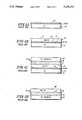
- FIGS. 1A-1Dshow cross-sections of a wafer at various stages of fabrication according to the prior art
- FIG. 2shows a cross-section of a wafer formed according to the prior art with N+ diffusions in a P type region
- FIGS. 3A-3Dshow a cross-section of a wafer at various stages of fabrication according to the principles of the present invention.
- FIG. 4shows a cross-section of a wafer incorporating the principles of the present invention including N+ diffusions in a P type region.
- FIGS. 3A-3D and 4having the same or similar purpose and function as that in FIGS. 1A-1D and 2 have the same reference numbers.
- a first wafer 10has a thin layer of silicon-germanium 12 formed thereon by CVD or MBE (molecular beam epitaxy). Step 3A does not differ from step 1A of the prior art.
- the structureis illustrated in FIG. 3B.
- the original substrate 10is then removed down to the silicon-germanium layer 12.
- layer 10may be removed by grinding, polishing and etching (using a strain sensitive etch) down to the silicon-germanium layer 12. This leaves the second substrate or handle 20 and the insulative layer 18 with the silicon-germanium layer 12 thereon as illustrated in FIG. 3C.
- an epitaxial layer 14is grown on the silicon-germanium layer 12 using the silicon-germanium layer 12 as a seed.
- the resulting structure as illustrated in FIG. 3Dincludes a top surface 17 in which devices are to be formed and a bottom surface 16 forming an interface between the epitaxial silicon layer 14 and the silicon-germanium layer 12.
- the surface 17 of FIG. 3D into which devices are to be builtis an untreated surface with a minimum of defects compared to the modified surface 16' of FIG. 1D.
- strainis created by mismatch between silicon and germanium atoms in the silicon-germanium layer 12. This strain has a gettering effect which removes oxygen and metal contaminants from the epitaxial layer 14, producing a denuded zone which can encompass the entire thickness of layer 14. The crystal quality of the epitaxial layer 14 is thereby enhanced. In addition, the strain within the silicon-germanium layer 12 leads to a low minority carrier lifetime in this layer.
- N+ type impuritiesare introduced to form regions 22 down to the insulated layer 18, as in FIG. 4.
- the N+ regions 22may represent the drain and source regions of an NMOSFET device, for example.
- the silicon-germanium layer 12 forming the interface between the insulative layer 18 and the epitaxial layer 14substantially reduces the formation of a back channel along the surface 24 between the regions 22 due to the low minority carrier lifetime in the silicon-germanium layer 12.
- a typical example of dimensionswould be the handle 20 having a thickness in the range of 10 to 25 mils, the insulative layer 18 having a thickness in the range of 1000 angstroms to 4 microns, the silicon-germanium layer 12 having a thickness in the range of 100 to 3000 angstroms and the epitaxial layer 14 having a thickness in the range of 1000 angstroms to 20 microns.
Landscapes
- Engineering & Computer Science (AREA)
- Physics & Mathematics (AREA)
- Condensed Matter Physics & Semiconductors (AREA)
- General Physics & Mathematics (AREA)
- Manufacturing & Machinery (AREA)
- Computer Hardware Design (AREA)
- Microelectronics & Electronic Packaging (AREA)
- Power Engineering (AREA)
- Recrystallisation Techniques (AREA)
Abstract
Description
Claims (10)
Priority Applications (1)
| Application Number | Priority Date | Filing Date | Title |
|---|---|---|---|
| US07/891,052US5218213A (en) | 1991-02-22 | 1992-06-01 | SOI wafer with sige |
Applications Claiming Priority (2)
| Application Number | Priority Date | Filing Date | Title |
|---|---|---|---|
| US65955391A | 1991-02-22 | 1991-02-22 | |
| US07/891,052US5218213A (en) | 1991-02-22 | 1992-06-01 | SOI wafer with sige |
Related Parent Applications (1)
| Application Number | Title | Priority Date | Filing Date |
|---|---|---|---|
| US65955391ADivision | 1991-02-22 | 1991-02-22 |
Publications (1)
| Publication Number | Publication Date |
|---|---|
| US5218213Atrue US5218213A (en) | 1993-06-08 |
Family
ID=27097847
Family Applications (1)
| Application Number | Title | Priority Date | Filing Date |
|---|---|---|---|
| US07/891,052Expired - LifetimeUS5218213A (en) | 1991-02-22 | 1992-06-01 | SOI wafer with sige |
Country Status (1)
| Country | Link |
|---|---|
| US (1) | US5218213A (en) |
Cited By (32)
| Publication number | Priority date | Publication date | Assignee | Title |
|---|---|---|---|---|
| EP0652591A1 (en)* | 1993-10-28 | 1995-05-10 | International Business Machines Corporation | Oxide in silicon-on-insulator structures |
| US5461243A (en)* | 1993-10-29 | 1995-10-24 | International Business Machines Corporation | Substrate for tensilely strained semiconductor |
| US5479048A (en)* | 1994-02-04 | 1995-12-26 | Analog Devices, Inc. | Integrated circuit chip supported by a handle wafer and provided with means to maintain the handle wafer potential at a desired level |
| DE4423067A1 (en)* | 1994-07-01 | 1996-01-04 | Daimler Benz Ag | Insulated semiconductor substrate prodn. method |
| US5665981A (en)* | 1994-10-24 | 1997-09-09 | Micron Technology, Inc. | Thin film transistors and method of promoting large crystal grain size in the formation of polycrystalline silicon alloy thin films |
| WO1998009804A1 (en)* | 1996-09-04 | 1998-03-12 | Sibond L.L.C. | Flattening process for bonded semiconductor substrates |
| US5892292A (en)* | 1994-06-03 | 1999-04-06 | Lucent Technologies Inc. | Getterer for multi-layer wafers and method for making same |
| US6258664B1 (en) | 1999-02-16 | 2001-07-10 | Micron Technology, Inc. | Methods of forming silicon-comprising materials having roughened outer surfaces, and methods of forming capacitor constructions |
| US6509587B2 (en) | 2000-09-29 | 2003-01-21 | Kabushiki Kaisha Toshiba | Semiconductor device |
| US6607968B1 (en)* | 1999-06-14 | 2003-08-19 | France Telecom | Method for making a silicon substrate comprising a buried thin silicon oxide film |
| US6607948B1 (en) | 1998-12-24 | 2003-08-19 | Kabushiki Kaisha Toshiba | Method of manufacturing a substrate using an SiGe layer |
| US6633066B1 (en) | 2000-01-07 | 2003-10-14 | Samsung Electronics Co., Ltd. | CMOS integrated circuit devices and substrates having unstrained silicon active layers |
| US20030230778A1 (en)* | 2002-01-30 | 2003-12-18 | Sumitomo Mitsubishi Silicon Corporation | SOI structure having a SiGe Layer interposed between the silicon and the insulator |
| US6690043B1 (en)* | 1999-11-26 | 2004-02-10 | Kabushiki Kaisha Toshiba | Semiconductor device and method of manufacturing the same |
| US20040178826A1 (en)* | 2003-03-11 | 2004-09-16 | Arup Bhattacharyya | Logic constructions and electronic devices |
| US20060022266A1 (en)* | 2004-07-30 | 2006-02-02 | International Business Machines Corporation | Manufacturable recessed strained rsd structure and process for advanced cmos |
| US20060138580A1 (en)* | 2004-12-20 | 2006-06-29 | Tae-Jin Kim | Photo-detecting device and related method of formation |
| US20070005052A1 (en)* | 2005-06-15 | 2007-01-04 | Kampa Gregory J | Treatment and diagnostic catheters with hydrogel electrodes |
| US20070202639A1 (en)* | 2004-12-14 | 2007-08-30 | International Business Machines Corporation | Dual stressed soi substrates |
| GB2437995A (en)* | 2006-05-11 | 2007-11-14 | X Fab Semiconductor Foundries | Semiconductor processing |
| US20080169512A1 (en)* | 2004-08-10 | 2008-07-17 | Doyle Brian S | Non-planar pMOS structure with a strained channel region and an integrated strained CMOS flow |
| US20080290525A1 (en)* | 2007-05-21 | 2008-11-27 | International Business Machines Corporation | Silicon-on-insulator structures for through via in silicon carriers |
| US20090149012A1 (en)* | 2004-09-30 | 2009-06-11 | Brask Justin K | Method of forming a nonplanar transistor with sidewall spacers |
| US7736956B2 (en) | 2005-08-17 | 2010-06-15 | Intel Corporation | Lateral undercut of metal gate in SOI device |
| US20100200917A1 (en)* | 2003-06-27 | 2010-08-12 | Hareland Scott A | Nonplanar device with stress incorporation layer and method of fabrication |
| US8067818B2 (en) | 2004-10-25 | 2011-11-29 | Intel Corporation | Nonplanar device with thinned lower body portion and method of fabrication |
| US8084818B2 (en) | 2004-06-30 | 2011-12-27 | Intel Corporation | High mobility tri-gate devices and methods of fabrication |
| US8183646B2 (en) | 2005-02-23 | 2012-05-22 | Intel Corporation | Field effect transistor with narrow bandgap source and drain regions and method of fabrication |
| EP2005477A4 (en)* | 2006-03-30 | 2012-06-13 | Freescale Semiconductor Inc | SEMICONDUCTOR MANUFACTURING METHOD USING ETCH STOPPING LAYER TO OPTIMIZE THE CONSTITUTION OF SOURCE / DRAIN STRESS ELEMENTS |
| US8268709B2 (en) | 2004-09-29 | 2012-09-18 | Intel Corporation | Independently accessed double-gate and tri-gate transistors in same process flow |
| US8362566B2 (en) | 2008-06-23 | 2013-01-29 | Intel Corporation | Stress in trigate devices using complimentary gate fill materials |
| US20210305131A1 (en)* | 2016-04-15 | 2021-09-30 | Taiwan Semiconductor Manufacturing Company Ltd. | Semiconductor structure and manufacturing method thereof |
Citations (6)
| Publication number | Priority date | Publication date | Assignee | Title |
|---|---|---|---|---|
| US4861393A (en)* | 1983-10-28 | 1989-08-29 | American Telephone And Telegraph Company, At&T Bell Laboratories | Semiconductor heterostructures having Gex Si1-x layers on Si utilizing molecular beam epitaxy |
| US4891329A (en)* | 1988-11-29 | 1990-01-02 | University Of North Carolina | Method of forming a nonsilicon semiconductor on insulator structure |
| US4962051A (en)* | 1988-11-18 | 1990-10-09 | Motorola, Inc. | Method of forming a defect-free semiconductor layer on insulator |
| US4975387A (en)* | 1989-12-15 | 1990-12-04 | The United States Of America As Represented By The Secretary Of The Navy | Formation of epitaxial si-ge heterostructures by solid phase epitaxy |
| US5006912A (en)* | 1987-04-14 | 1991-04-09 | British Telecommunications Public Limited Company | Heterojunction bipolar transistor with SiGe |
| US5013681A (en)* | 1989-09-29 | 1991-05-07 | The United States Of America As Represented By The Secretary Of The Navy | Method of producing a thin silicon-on-insulator layer |
- 1992
- 1992-06-01USUS07/891,052patent/US5218213A/ennot_activeExpired - Lifetime
Patent Citations (6)
| Publication number | Priority date | Publication date | Assignee | Title |
|---|---|---|---|---|
| US4861393A (en)* | 1983-10-28 | 1989-08-29 | American Telephone And Telegraph Company, At&T Bell Laboratories | Semiconductor heterostructures having Gex Si1-x layers on Si utilizing molecular beam epitaxy |
| US5006912A (en)* | 1987-04-14 | 1991-04-09 | British Telecommunications Public Limited Company | Heterojunction bipolar transistor with SiGe |
| US4962051A (en)* | 1988-11-18 | 1990-10-09 | Motorola, Inc. | Method of forming a defect-free semiconductor layer on insulator |
| US4891329A (en)* | 1988-11-29 | 1990-01-02 | University Of North Carolina | Method of forming a nonsilicon semiconductor on insulator structure |
| US5013681A (en)* | 1989-09-29 | 1991-05-07 | The United States Of America As Represented By The Secretary Of The Navy | Method of producing a thin silicon-on-insulator layer |
| US4975387A (en)* | 1989-12-15 | 1990-12-04 | The United States Of America As Represented By The Secretary Of The Navy | Formation of epitaxial si-ge heterostructures by solid phase epitaxy |
Non-Patent Citations (4)
| Title |
|---|
| Haisma et al., "Silicon-on-Insulator Wafer Bonding-Wafer Thinning, Technological Evaluations," Japanese J. Appl. Phys., vol. 28, No. 8, 1989, pp. 1426-1443. |
| Haisma et al., Silicon on Insulator Wafer Bonding Wafer Thinning, Technological Evaluations, Japanese J. Appl. Phys., vol. 28, No. 8, 1989, pp. 1426 1443.* |
| Kimura et al., "Epitaxial Film Transfer Technique for Producing Single Crystal Si Film on an Insulating Substrate," Appl. Phys. Lett. 43(3), Aug. 1, 1983, pp. 263-265. |
| Kimura et al., Epitaxial Film Transfer Technique for Producing Single Crystal Si Film on an Insulating Substrate, Appl. Phys. Lett. 43(3), Aug. 1, 1983, pp. 263 265.* |
Cited By (82)
| Publication number | Priority date | Publication date | Assignee | Title |
|---|---|---|---|---|
| EP0652591A1 (en)* | 1993-10-28 | 1995-05-10 | International Business Machines Corporation | Oxide in silicon-on-insulator structures |
| US5461243A (en)* | 1993-10-29 | 1995-10-24 | International Business Machines Corporation | Substrate for tensilely strained semiconductor |
| US5479048A (en)* | 1994-02-04 | 1995-12-26 | Analog Devices, Inc. | Integrated circuit chip supported by a handle wafer and provided with means to maintain the handle wafer potential at a desired level |
| US5569621A (en)* | 1994-02-04 | 1996-10-29 | Analog Devices, Incorporated | Integrated circuit chip supported by a handle wafer and provided with means to maintain the handle wafer potential at a desired level |
| US5892292A (en)* | 1994-06-03 | 1999-04-06 | Lucent Technologies Inc. | Getterer for multi-layer wafers and method for making same |
| DE4423067A1 (en)* | 1994-07-01 | 1996-01-04 | Daimler Benz Ag | Insulated semiconductor substrate prodn. method |
| US5977560A (en)* | 1994-10-24 | 1999-11-02 | Micron Technology, Inc. | Thin film transistor constructions with polycrystalline silicon-germanium alloy doped with carbon in the channel region |
| US6320202B1 (en) | 1994-10-24 | 2001-11-20 | Micron Technology, Inc. | Bottom-gated thin film transistors comprising germanium in a channel region |
| US5665981A (en)* | 1994-10-24 | 1997-09-09 | Micron Technology, Inc. | Thin film transistors and method of promoting large crystal grain size in the formation of polycrystalline silicon alloy thin films |
| WO1998009804A1 (en)* | 1996-09-04 | 1998-03-12 | Sibond L.L.C. | Flattening process for bonded semiconductor substrates |
| US20040070051A1 (en)* | 1998-12-24 | 2004-04-15 | Kabushiki Kaisha Toshiba | Semiconductor device and method of manufacturing substrate |
| US6607948B1 (en) | 1998-12-24 | 2003-08-19 | Kabushiki Kaisha Toshiba | Method of manufacturing a substrate using an SiGe layer |
| US6917096B2 (en) | 1998-12-24 | 2005-07-12 | Kabushiki Kaisha Toshiba | Semiconductor device and method of manufacturing substrate |
| US6258664B1 (en) | 1999-02-16 | 2001-07-10 | Micron Technology, Inc. | Methods of forming silicon-comprising materials having roughened outer surfaces, and methods of forming capacitor constructions |
| US6607968B1 (en)* | 1999-06-14 | 2003-08-19 | France Telecom | Method for making a silicon substrate comprising a buried thin silicon oxide film |
| USRE41841E1 (en) | 1999-06-14 | 2010-10-19 | Malgorzata Jurczak | Method for making a silicon substrate comprising a buried thin silicon oxide film |
| US6690043B1 (en)* | 1999-11-26 | 2004-02-10 | Kabushiki Kaisha Toshiba | Semiconductor device and method of manufacturing the same |
| US20040126958A1 (en)* | 1999-11-26 | 2004-07-01 | Koji Usuda | Semiconductor device and method of manufacturing the same |
| US7033913B2 (en) | 1999-11-26 | 2006-04-25 | Kabushiki Kaisha Toshiba | Semiconductor device and method of manufacturing the same |
| US7642140B2 (en) | 2000-01-07 | 2010-01-05 | Samsung Electronics Co., Ltd. | CMOS integrated circuit devices and substrates having buried silicon germanium layers therein and method of forming same |
| US20040075143A1 (en)* | 2000-01-07 | 2004-04-22 | Geum-Jong Bae | CMOS integrated circuit devices and substrates having buried silicon germanium layers therein and methods of forming same |
| US7195987B2 (en) | 2000-01-07 | 2007-03-27 | Samsung Electronics Co., Ltd. | Methods of forming CMOS integrated circuit devices and substrates having buried silicon germanium layers therein |
| US20070117297A1 (en)* | 2000-01-07 | 2007-05-24 | Geum-Jong Bae | CMOS integrated circuit devices and substrates having buried silicon germanium layers therein and method of forming same |
| US6914301B2 (en) | 2000-01-07 | 2005-07-05 | Samsung Electronics Co., Ltd. | CMOS integrated circuit devices and substrates having buried silicon germanium layers therein and methods of forming same |
| US6633066B1 (en) | 2000-01-07 | 2003-10-14 | Samsung Electronics Co., Ltd. | CMOS integrated circuit devices and substrates having unstrained silicon active layers |
| US20050230676A1 (en)* | 2000-01-07 | 2005-10-20 | Geum-Jong Bae | Methods of forming CMOS integrated circuit devices and substrates having buried silicon germanium layers therein and devices so formed |
| US6509587B2 (en) | 2000-09-29 | 2003-01-21 | Kabushiki Kaisha Toshiba | Semiconductor device |
| US20030230778A1 (en)* | 2002-01-30 | 2003-12-18 | Sumitomo Mitsubishi Silicon Corporation | SOI structure having a SiGe Layer interposed between the silicon and the insulator |
| US20060063356A1 (en)* | 2002-01-30 | 2006-03-23 | Sumitomo Mitsubishi Silicon Corporation | SOI structure having a sige layer interposed between the silicon and the insulator |
| US7741193B2 (en) | 2002-01-30 | 2010-06-22 | Sumitomo Mitsubishi Silicon Corp. | SOI structure having a SiGe layer interposed between the silicon and the insulator |
| US20050242396A1 (en)* | 2002-01-30 | 2005-11-03 | Sumitomo Mitsubishi Silicon Corporation | SOI structure having a sige layer interposed between the silicon and the insulator |
| US7180138B2 (en) | 2002-01-30 | 2007-02-20 | Sumitomo Mitsubishi Silicon Corp. | SOI structure having a SiGe layer interposed between the silicon and the insulator |
| US7947572B2 (en) | 2002-01-30 | 2011-05-24 | Sumitomo Mitsubishi Silicon Corp. | Method of manufacturing a SOI structure having a SiGe layer interposed between the silicon and the insulator |
| US20060011978A1 (en)* | 2003-03-11 | 2006-01-19 | Arup Bhattacharyya | Semiconductor constructions and integrated circuits |
| US20040178826A1 (en)* | 2003-03-11 | 2004-09-16 | Arup Bhattacharyya | Logic constructions and electronic devices |
| US6900667B2 (en)* | 2003-03-11 | 2005-05-31 | Micron Technology, Inc. | Logic constructions and electronic devices |
| US20060157688A1 (en)* | 2003-03-11 | 2006-07-20 | Micron Technology, Inc. | Methods of forming semiconductor constructions and integrated circuits |
| US8405164B2 (en) | 2003-06-27 | 2013-03-26 | Intel Corporation | Tri-gate transistor device with stress incorporation layer and method of fabrication |
| US20100200917A1 (en)* | 2003-06-27 | 2010-08-12 | Hareland Scott A | Nonplanar device with stress incorporation layer and method of fabrication |
| US8084818B2 (en) | 2004-06-30 | 2011-12-27 | Intel Corporation | High mobility tri-gate devices and methods of fabrication |
| US20060022266A1 (en)* | 2004-07-30 | 2006-02-02 | International Business Machines Corporation | Manufacturable recessed strained rsd structure and process for advanced cmos |
| US7115955B2 (en) | 2004-07-30 | 2006-10-03 | International Business Machines Corporation | Semiconductor device having a strained raised source/drain |
| US7446005B2 (en) | 2004-07-30 | 2008-11-04 | International Business Machines Corporation | Manufacturable recessed strained RSD structure and process for advanced CMOS |
| US20060205189A1 (en)* | 2004-07-30 | 2006-09-14 | International Business Machines Corporation | Manufacturable recessed strained RSD structure and process for advanced CMOS |
| US20080169512A1 (en)* | 2004-08-10 | 2008-07-17 | Doyle Brian S | Non-planar pMOS structure with a strained channel region and an integrated strained CMOS flow |
| US7960794B2 (en) | 2004-08-10 | 2011-06-14 | Intel Corporation | Non-planar pMOS structure with a strained channel region and an integrated strained CMOS flow |
| US8399922B2 (en) | 2004-09-29 | 2013-03-19 | Intel Corporation | Independently accessed double-gate and tri-gate transistors |
| US8268709B2 (en) | 2004-09-29 | 2012-09-18 | Intel Corporation | Independently accessed double-gate and tri-gate transistors in same process flow |
| US20090149012A1 (en)* | 2004-09-30 | 2009-06-11 | Brask Justin K | Method of forming a nonplanar transistor with sidewall spacers |
| US10236356B2 (en) | 2004-10-25 | 2019-03-19 | Intel Corporation | Nonplanar device with thinned lower body portion and method of fabrication |
| US9741809B2 (en) | 2004-10-25 | 2017-08-22 | Intel Corporation | Nonplanar device with thinned lower body portion and method of fabrication |
| US9190518B2 (en) | 2004-10-25 | 2015-11-17 | Intel Corporation | Nonplanar device with thinned lower body portion and method of fabrication |
| US8749026B2 (en) | 2004-10-25 | 2014-06-10 | Intel Corporation | Nonplanar device with thinned lower body portion and method of fabrication |
| US8067818B2 (en) | 2004-10-25 | 2011-11-29 | Intel Corporation | Nonplanar device with thinned lower body portion and method of fabrication |
| US8502351B2 (en) | 2004-10-25 | 2013-08-06 | Intel Corporation | Nonplanar device with thinned lower body portion and method of fabrication |
| US7312134B2 (en)* | 2004-12-14 | 2007-12-25 | International Business Machines Corporation | Dual stressed SOI substrates |
| US20070202639A1 (en)* | 2004-12-14 | 2007-08-30 | International Business Machines Corporation | Dual stressed soi substrates |
| US20060138580A1 (en)* | 2004-12-20 | 2006-06-29 | Tae-Jin Kim | Photo-detecting device and related method of formation |
| US7420207B2 (en)* | 2004-12-20 | 2008-09-02 | Samsung Electronics Co., Ltd. | Photo-detecting device and related method of formation |
| US8368135B2 (en) | 2005-02-23 | 2013-02-05 | Intel Corporation | Field effect transistor with narrow bandgap source and drain regions and method of fabrication |
| US10121897B2 (en) | 2005-02-23 | 2018-11-06 | Intel Corporation | Field effect transistor with narrow bandgap source and drain regions and method of fabrication |
| US8183646B2 (en) | 2005-02-23 | 2012-05-22 | Intel Corporation | Field effect transistor with narrow bandgap source and drain regions and method of fabrication |
| US9748391B2 (en) | 2005-02-23 | 2017-08-29 | Intel Corporation | Field effect transistor with narrow bandgap source and drain regions and method of fabrication |
| US8664694B2 (en) | 2005-02-23 | 2014-03-04 | Intel Corporation | Field effect transistor with narrow bandgap source and drain regions and method of fabrication |
| US9614083B2 (en) | 2005-02-23 | 2017-04-04 | Intel Corporation | Field effect transistor with narrow bandgap source and drain regions and method of fabrication |
| US9368583B2 (en) | 2005-02-23 | 2016-06-14 | Intel Corporation | Field effect transistor with narrow bandgap source and drain regions and method of fabrication |
| US8816394B2 (en) | 2005-02-23 | 2014-08-26 | Intel Corporation | Field effect transistor with narrow bandgap source and drain regions and method of fabrication |
| US9048314B2 (en) | 2005-02-23 | 2015-06-02 | Intel Corporation | Field effect transistor with narrow bandgap source and drain regions and method of fabrication |
| US20070005052A1 (en)* | 2005-06-15 | 2007-01-04 | Kampa Gregory J | Treatment and diagnostic catheters with hydrogel electrodes |
| US7736956B2 (en) | 2005-08-17 | 2010-06-15 | Intel Corporation | Lateral undercut of metal gate in SOI device |
| EP2005477A4 (en)* | 2006-03-30 | 2012-06-13 | Freescale Semiconductor Inc | SEMICONDUCTOR MANUFACTURING METHOD USING ETCH STOPPING LAYER TO OPTIMIZE THE CONSTITUTION OF SOURCE / DRAIN STRESS ELEMENTS |
| GB2437995A (en)* | 2006-05-11 | 2007-11-14 | X Fab Semiconductor Foundries | Semiconductor processing |
| US20090309190A1 (en)* | 2006-05-11 | 2009-12-17 | William Andrew Nevin | Semiconductor processing |
| CN101312161B (en)* | 2007-05-21 | 2010-12-01 | 国际商业机器公司 | Electronic structures and fabrication methods thereof |
| US20080290525A1 (en)* | 2007-05-21 | 2008-11-27 | International Business Machines Corporation | Silicon-on-insulator structures for through via in silicon carriers |
| US7645701B2 (en)* | 2007-05-21 | 2010-01-12 | International Business Machines Corporation | Silicon-on-insulator structures for through via in silicon carriers |
| US9224754B2 (en) | 2008-06-23 | 2015-12-29 | Intel Corporation | Stress in trigate devices using complimentary gate fill materials |
| US9450092B2 (en) | 2008-06-23 | 2016-09-20 | Intel Corporation | Stress in trigate devices using complimentary gate fill materials |
| US8741733B2 (en) | 2008-06-23 | 2014-06-03 | Intel Corporation | Stress in trigate devices using complimentary gate fill materials |
| US9806193B2 (en) | 2008-06-23 | 2017-10-31 | Intel Corporation | Stress in trigate devices using complimentary gate fill materials |
| US8362566B2 (en) | 2008-06-23 | 2013-01-29 | Intel Corporation | Stress in trigate devices using complimentary gate fill materials |
| US20210305131A1 (en)* | 2016-04-15 | 2021-09-30 | Taiwan Semiconductor Manufacturing Company Ltd. | Semiconductor structure and manufacturing method thereof |
Similar Documents
| Publication | Publication Date | Title |
|---|---|---|
| US5240876A (en) | Method of fabricating SOI wafer with SiGe as an etchback film in a BESOI process | |
| US5218213A (en) | SOI wafer with sige | |
| US5034343A (en) | Manufacturing ultra-thin wafer using a handle wafer | |
| US6963078B2 (en) | Dual strain-state SiGe layers for microelectronics | |
| US6723622B2 (en) | Method of forming a germanium film on a semiconductor substrate that includes the formation of a graded silicon-germanium buffer layer prior to the formation of a germanium layer | |
| US7442657B2 (en) | Producing stress-relaxed crystalline layer on a substrate | |
| KR100473663B1 (en) | Method for producing cmos device | |
| KR100392166B1 (en) | Semiconductor device and method for manufacturing the same | |
| US7825470B2 (en) | Transistor and in-situ fabrication process | |
| US4948742A (en) | Method of manufacturing a semiconductor device | |
| JP4949628B2 (en) | Method for protecting a strained semiconductor substrate layer during a CMOS process | |
| EP0253059A2 (en) | Process for suppressing the rise of the buried layer of a semiconductor device | |
| JPH0719839B2 (en) | Method for manufacturing semiconductor substrate | |
| JPH08116038A (en) | Semiconductor device and manufacturing method thereof | |
| US6211095B1 (en) | Method for relieving lattice mismatch stress in semiconductor devices | |
| US20060211221A1 (en) | Method for producing a strained layer on a substrate and corresponding layer structure | |
| US20040253458A1 (en) | Semiconductor wafer and method of manufacturing thereof | |
| US20030160300A1 (en) | Semiconductor substrate, method of manufacturing the same and semiconductor device | |
| JPH0469814B2 (en) | ||
| US5420458A (en) | Semiconductor device and method of manufacture thereof | |
| US5433168A (en) | Method of producing semiconductor substrate | |
| US7220626B2 (en) | Structure and method for manufacturing planar strained Si/SiGe substrate with multiple orientations and different stress levels | |
| US7749817B2 (en) | Single-crystal layer on a dielectric layer | |
| US5352628A (en) | Method of forming diffusion region of semiconductor device by solid phase diffusion | |
| JP3901957B2 (en) | Semiconductor substrate manufacturing method and semiconductor device manufactured by the method |
Legal Events
| Date | Code | Title | Description |
|---|---|---|---|
| STCF | Information on status: patent grant | Free format text:PATENTED CASE | |
| FEPP | Fee payment procedure | Free format text:PAYOR NUMBER ASSIGNED (ORIGINAL EVENT CODE: ASPN); ENTITY STATUS OF PATENT OWNER: LARGE ENTITY | |
| FPAY | Fee payment | Year of fee payment:4 | |
| AS | Assignment | Owner name:INTERSIL CORPORATION, FLORIDA Free format text:ASSIGNMENT OF ASSIGNORS INTEREST;ASSIGNOR:HARRIS CORPORATION;REEL/FRAME:010247/0043 Effective date:19990813 | |
| AS | Assignment | Owner name:CREDIT SUISSE FIRST BOSTON, AS COLLATERAL AGENT, N Free format text:SECURITY INTEREST;ASSIGNOR:INTERSIL CORPORATION;REEL/FRAME:010351/0410 Effective date:19990813 | |
| FPAY | Fee payment | Year of fee payment:8 | |
| REMI | Maintenance fee reminder mailed | ||
| FPAY | Fee payment | Year of fee payment:12 | |
| AS | Assignment | Owner name:MORGAN STANLEY & CO. INCORPORATED,NEW YORK Free format text:SECURITY AGREEMENT;ASSIGNORS:INTERSIL CORPORATION;TECHWELL, INC.;INTERSIL COMMUNICATIONS, INC.;AND OTHERS;REEL/FRAME:024390/0608 Effective date:20100427 | |
| AS | Assignment | Owner name:INTERSIL CORPORATION,FLORIDA Free format text:RELEASE BY SECURED PARTY;ASSIGNOR:CREDIT SUISSE FIRST BOSTON;REEL/FRAME:024445/0049 Effective date:20030306 |