US5212147A - Method of forming a patterned in-situ high Tc superconductive film - Google Patents
Method of forming a patterned in-situ high Tc superconductive filmDownload PDFInfo
- Publication number
- US5212147A US5212147AUS07/700,671US70067191AUS5212147AUS 5212147 AUS5212147 AUS 5212147AUS 70067191 AUS70067191 AUS 70067191AUS 5212147 AUS5212147 AUS 5212147A
- Authority
- US
- United States
- Prior art keywords
- layer
- sacrificial
- superconductive
- substrate
- gap
- Prior art date
- Legal status (The legal status is an assumption and is not a legal conclusion. Google has not performed a legal analysis and makes no representation as to the accuracy of the status listed.)
- Expired - Lifetime
Links
- 238000000034methodMethods0.000titleclaimsabstractdescription45
- 238000011065in-situ storageMethods0.000titleclaimsabstractdescription13
- 239000000463materialSubstances0.000claimsabstractdescription67
- 239000000758substrateSubstances0.000claimsabstractdescription47
- 238000000151depositionMethods0.000claimsabstractdescription41
- 229920000642polymerPolymers0.000claimsabstractdescription36
- 229920002120photoresistant polymerPolymers0.000claimsabstractdescription24
- 238000005530etchingMethods0.000claimsdescription18
- 229910052758niobiumInorganic materials0.000claimsdescription13
- 229910052709silverInorganic materials0.000claimsdescription13
- BQCADISMDOOEFD-UHFFFAOYSA-NSilverChemical compound[Ag]BQCADISMDOOEFD-UHFFFAOYSA-N0.000claimsdescription12
- 239000004332silverSubstances0.000claimsdescription12
- 230000000873masking effectEffects0.000claimsdescription10
- 239000011248coating agentSubstances0.000claimsdescription6
- 238000000576coating methodMethods0.000claimsdescription6
- PCHJSUWPFVWCPO-UHFFFAOYSA-NgoldChemical compound[Au]PCHJSUWPFVWCPO-UHFFFAOYSA-N0.000claimsdescription6
- 229910052737goldInorganic materials0.000claimsdescription6
- 239000010931goldSubstances0.000claimsdescription6
- PXHVJJICTQNCMI-UHFFFAOYSA-NNickelChemical compound[Ni]PXHVJJICTQNCMI-UHFFFAOYSA-N0.000claimsdescription4
- 239000010949copperSubstances0.000claimsdescription4
- 230000008020evaporationEffects0.000claimsdescription4
- 238000001704evaporationMethods0.000claimsdescription4
- 229910052710siliconInorganic materials0.000claimsdescription3
- RYGMFSIKBFXOCR-UHFFFAOYSA-NCopperChemical compound[Cu]RYGMFSIKBFXOCR-UHFFFAOYSA-N0.000claimsdescription2
- 229910052802copperInorganic materials0.000claimsdescription2
- 229910052751metalInorganic materials0.000claimsdescription2
- 239000002184metalSubstances0.000claimsdescription2
- 229910052750molybdenumInorganic materials0.000claimsdescription2
- 229910052759nickelInorganic materials0.000claimsdescription2
- 229910052715tantalumInorganic materials0.000claimsdescription2
- 229910052721tungstenInorganic materials0.000claimsdescription2
- 238000007493shaping processMethods0.000claims3
- 230000002411adverseEffects0.000abstractdescription4
- 238000001020plasma etchingMethods0.000abstractdescription4
- 238000005137deposition processMethods0.000abstractdescription3
- 238000012545processingMethods0.000description13
- 230000008021depositionEffects0.000description12
- 239000010955niobiumSubstances0.000description12
- GUCVJGMIXFAOAE-UHFFFAOYSA-Nniobium atomChemical compound[Nb]GUCVJGMIXFAOAE-UHFFFAOYSA-N0.000description12
- 239000000243solutionSubstances0.000description11
- 238000000059patterningMethods0.000description9
- 238000000992sputter etchingMethods0.000description7
- 230000015572biosynthetic processEffects0.000description5
- VYPSYNLAJGMNEJ-UHFFFAOYSA-NSilicium dioxideChemical compoundO=[Si]=OVYPSYNLAJGMNEJ-UHFFFAOYSA-N0.000description4
- 239000002253acidSubstances0.000description4
- 230000000877morphologic effectEffects0.000description4
- 239000010703siliconSubstances0.000description4
- 238000004528spin coatingMethods0.000description4
- XUIMIQQOPSSXEZ-UHFFFAOYSA-NSiliconChemical compound[Si]XUIMIQQOPSSXEZ-UHFFFAOYSA-N0.000description3
- 230000002378acidificating effectEffects0.000description3
- QVGXLLKOCUKJST-UHFFFAOYSA-Natomic oxygenChemical compound[O]QVGXLLKOCUKJST-UHFFFAOYSA-N0.000description3
- 229910052760oxygenInorganic materials0.000description3
- 239000001301oxygenSubstances0.000description3
- LFQSCWFLJHTTHZ-UHFFFAOYSA-NEthanolChemical compoundCCOLFQSCWFLJHTTHZ-UHFFFAOYSA-N0.000description2
- GRYLNZFGIOXLOG-UHFFFAOYSA-NNitric acidChemical compoundO[N+]([O-])=OGRYLNZFGIOXLOG-UHFFFAOYSA-N0.000description2
- 230000015556catabolic processEffects0.000description2
- 238000011109contaminationMethods0.000description2
- 238000006731degradation reactionMethods0.000description2
- 238000007737ion beam depositionMethods0.000description2
- 238000010884ion-beam techniqueMethods0.000description2
- 238000013508migrationMethods0.000description2
- 230000005012migrationEffects0.000description2
- 229910017604nitric acidInorganic materials0.000description2
- 230000002829reductive effectEffects0.000description2
- 235000012239silicon dioxideNutrition0.000description2
- 239000000377silicon dioxideSubstances0.000description2
- 229910052814silicon oxideInorganic materials0.000description2
- XLYOFNOQVPJJNP-UHFFFAOYSA-NwaterSubstancesOXLYOFNOQVPJJNP-UHFFFAOYSA-N0.000description2
- WKBOTKDWSSQWDR-UHFFFAOYSA-NBromine atomChemical compound[Br]WKBOTKDWSSQWDR-UHFFFAOYSA-N0.000description1
- QPLDLSVMHZLSFG-UHFFFAOYSA-NCopper oxideChemical class[Cu]=OQPLDLSVMHZLSFG-UHFFFAOYSA-N0.000description1
- KCXVZYZYPLLWCC-UHFFFAOYSA-NEDTAChemical compoundOC(=O)CN(CC(O)=O)CCN(CC(O)=O)CC(O)=OKCXVZYZYPLLWCC-UHFFFAOYSA-N0.000description1
- 229910002244LaAlO3Inorganic materials0.000description1
- 229910002331LaGaO3Inorganic materials0.000description1
- ZOKXTWBITQBERF-UHFFFAOYSA-NMolybdenumChemical compound[Mo]ZOKXTWBITQBERF-UHFFFAOYSA-N0.000description1
- 239000004642PolyimideSubstances0.000description1
- 239000003929acidic solutionSubstances0.000description1
- 238000000137annealingMethods0.000description1
- 239000011260aqueous acidSubstances0.000description1
- GDTBXPJZTBHREO-UHFFFAOYSA-NbromineSubstancesBrBrGDTBXPJZTBHREO-UHFFFAOYSA-N0.000description1
- 229910052794bromiumInorganic materials0.000description1
- 238000005266castingMethods0.000description1
- 239000000919ceramicSubstances0.000description1
- 238000005229chemical vapour depositionMethods0.000description1
- 238000007796conventional methodMethods0.000description1
- 239000013078crystalSubstances0.000description1
- 230000003413degradative effectEffects0.000description1
- 230000001419dependent effectEffects0.000description1
- 238000011161developmentMethods0.000description1
- 238000002474experimental methodMethods0.000description1
- SLGWESQGEUXWJQ-UHFFFAOYSA-Nformaldehyde;phenolChemical compoundO=C.OC1=CC=CC=C1SLGWESQGEUXWJQ-UHFFFAOYSA-N0.000description1
- 238000010438heat treatmentMethods0.000description1
- 238000010952in-situ formationMethods0.000description1
- 238000001659ion-beam spectroscopyMethods0.000description1
- 150000002500ionsChemical class0.000description1
- 238000000608laser ablationMethods0.000description1
- 230000000670limiting effectEffects0.000description1
- CPLXHLVBOLITMK-UHFFFAOYSA-Nmagnesium oxideInorganic materials[Mg]=OCPLXHLVBOLITMK-UHFFFAOYSA-N0.000description1
- 238000001465metallisationMethods0.000description1
- 150000002739metalsChemical class0.000description1
- 239000011733molybdenumSubstances0.000description1
- 239000012457nonaqueous mediaSubstances0.000description1
- 229920003986novolacPolymers0.000description1
- 230000035515penetrationEffects0.000description1
- 229920001568phenolic resinPolymers0.000description1
- 229920001721polyimidePolymers0.000description1
- 230000001681protective effectEffects0.000description1
- 239000004065semiconductorSubstances0.000description1
- 239000002904solventSubstances0.000description1
- 238000004544sputter depositionMethods0.000description1
- GUVRBAGPIYLISA-UHFFFAOYSA-Ntantalum atomChemical compound[Ta]GUVRBAGPIYLISA-UHFFFAOYSA-N0.000description1
- 238000012546transferMethods0.000description1
- WFKWXMTUELFFGS-UHFFFAOYSA-NtungstenChemical compound[W]WFKWXMTUELFFGS-UHFFFAOYSA-N0.000description1
- 239000010937tungstenSubstances0.000description1
- 238000001039wet etchingMethods0.000description1
Images

Classifications
- C—CHEMISTRY; METALLURGY
- C04—CEMENTS; CONCRETE; ARTIFICIAL STONE; CERAMICS; REFRACTORIES
- C04B—LIME, MAGNESIA; SLAG; CEMENTS; COMPOSITIONS THEREOF, e.g. MORTARS, CONCRETE OR LIKE BUILDING MATERIALS; ARTIFICIAL STONE; CERAMICS; REFRACTORIES; TREATMENT OF NATURAL STONE
- C04B41/00—After-treatment of mortars, concrete, artificial stone or ceramics; Treatment of natural stone
- C04B41/009—After-treatment of mortars, concrete, artificial stone or ceramics; Treatment of natural stone characterised by the material treated
- C—CHEMISTRY; METALLURGY
- C04—CEMENTS; CONCRETE; ARTIFICIAL STONE; CERAMICS; REFRACTORIES
- C04B—LIME, MAGNESIA; SLAG; CEMENTS; COMPOSITIONS THEREOF, e.g. MORTARS, CONCRETE OR LIKE BUILDING MATERIALS; ARTIFICIAL STONE; CERAMICS; REFRACTORIES; TREATMENT OF NATURAL STONE
- C04B41/00—After-treatment of mortars, concrete, artificial stone or ceramics; Treatment of natural stone
- C04B41/45—Coating or impregnating, e.g. injection in masonry, partial coating of green or fired ceramics, organic coating compositions for adhering together two concrete elements
- C04B41/4572—Partial coating or impregnation of the surface of the substrate
- C—CHEMISTRY; METALLURGY
- C04—CEMENTS; CONCRETE; ARTIFICIAL STONE; CERAMICS; REFRACTORIES
- C04B—LIME, MAGNESIA; SLAG; CEMENTS; COMPOSITIONS THEREOF, e.g. MORTARS, CONCRETE OR LIKE BUILDING MATERIALS; ARTIFICIAL STONE; CERAMICS; REFRACTORIES; TREATMENT OF NATURAL STONE
- C04B41/00—After-treatment of mortars, concrete, artificial stone or ceramics; Treatment of natural stone
- C04B41/45—Coating or impregnating, e.g. injection in masonry, partial coating of green or fired ceramics, organic coating compositions for adhering together two concrete elements
- C04B41/459—Temporary coatings or impregnations
- C04B41/4592—Temporary coatings or impregnations for masking purposes
- C04B41/4594—Temporary coatings or impregnations for masking purposes in metallisation processes
- C—CHEMISTRY; METALLURGY
- C04—CEMENTS; CONCRETE; ARTIFICIAL STONE; CERAMICS; REFRACTORIES
- C04B—LIME, MAGNESIA; SLAG; CEMENTS; COMPOSITIONS THEREOF, e.g. MORTARS, CONCRETE OR LIKE BUILDING MATERIALS; ARTIFICIAL STONE; CERAMICS; REFRACTORIES; TREATMENT OF NATURAL STONE
- C04B41/00—After-treatment of mortars, concrete, artificial stone or ceramics; Treatment of natural stone
- C04B41/45—Coating or impregnating, e.g. injection in masonry, partial coating of green or fired ceramics, organic coating compositions for adhering together two concrete elements
- C04B41/52—Multiple coating or impregnating multiple coating or impregnating with the same composition or with compositions only differing in the concentration of the constituents, is classified as single coating or impregnation
- C—CHEMISTRY; METALLURGY
- C04—CEMENTS; CONCRETE; ARTIFICIAL STONE; CERAMICS; REFRACTORIES
- C04B—LIME, MAGNESIA; SLAG; CEMENTS; COMPOSITIONS THEREOF, e.g. MORTARS, CONCRETE OR LIKE BUILDING MATERIALS; ARTIFICIAL STONE; CERAMICS; REFRACTORIES; TREATMENT OF NATURAL STONE
- C04B41/00—After-treatment of mortars, concrete, artificial stone or ceramics; Treatment of natural stone
- C04B41/80—After-treatment of mortars, concrete, artificial stone or ceramics; Treatment of natural stone of only ceramics
- C04B41/81—Coating or impregnation
- C04B41/89—Coating or impregnation for obtaining at least two superposed coatings having different compositions
- H—ELECTRICITY
- H10—SEMICONDUCTOR DEVICES; ELECTRIC SOLID-STATE DEVICES NOT OTHERWISE PROVIDED FOR
- H10N—ELECTRIC SOLID-STATE DEVICES NOT OTHERWISE PROVIDED FOR
- H10N60/00—Superconducting devices
- H10N60/01—Manufacture or treatment
- H10N60/0268—Manufacture or treatment of devices comprising copper oxide
- H10N60/0661—Processes performed after copper oxide formation, e.g. patterning
- Y—GENERAL TAGGING OF NEW TECHNOLOGICAL DEVELOPMENTS; GENERAL TAGGING OF CROSS-SECTIONAL TECHNOLOGIES SPANNING OVER SEVERAL SECTIONS OF THE IPC; TECHNICAL SUBJECTS COVERED BY FORMER USPC CROSS-REFERENCE ART COLLECTIONS [XRACs] AND DIGESTS
- Y10—TECHNICAL SUBJECTS COVERED BY FORMER USPC
- Y10S—TECHNICAL SUBJECTS COVERED BY FORMER USPC CROSS-REFERENCE ART COLLECTIONS [XRACs] AND DIGESTS
- Y10S505/00—Superconductor technology: apparatus, material, process
- Y10S505/725—Process of making or treating high tc, above 30 k, superconducting shaped material, article, or device
- Y10S505/728—Etching
- Y—GENERAL TAGGING OF NEW TECHNOLOGICAL DEVELOPMENTS; GENERAL TAGGING OF CROSS-SECTIONAL TECHNOLOGIES SPANNING OVER SEVERAL SECTIONS OF THE IPC; TECHNICAL SUBJECTS COVERED BY FORMER USPC CROSS-REFERENCE ART COLLECTIONS [XRACs] AND DIGESTS
- Y10—TECHNICAL SUBJECTS COVERED BY FORMER USPC
- Y10S—TECHNICAL SUBJECTS COVERED BY FORMER USPC CROSS-REFERENCE ART COLLECTIONS [XRACs] AND DIGESTS
- Y10S505/00—Superconductor technology: apparatus, material, process
- Y10S505/725—Process of making or treating high tc, above 30 k, superconducting shaped material, article, or device
- Y10S505/73—Vacuum treating or coating
- Y10S505/732—Evaporative coating with superconducting material
Definitions
- the present inventionrelates generally to superconductive materials and more particularly to methods of forming a superconductive film on a substrate.
- the methodincludes depositing a resist and patterning the resist to include somewhat overhung profiles, i.e., a gap in the resist is narrower at the top than at the bottom.
- the superconducting materialis then deposited using equipment which provides only normally incident deposition.
- the superconducting material on the resistis discontinuous with the superconducting material deposited on the substrate.
- the lift-off methodhas been used in the patterning of post-deposition annealed high T c superconductive films. However, the method does render the superconducting material more susceptible to particulate contamination.
- in-situ filmshave superior electrical and morphological characteristics, and therefore are generally preferred over post-deposition annealed films for device applications.
- electrical characteristicsin-situ films have superior critical current densities (J c ) and surface resistances (R s ).
- the filmstend to have improved grain boundaries and exhibit an improvement in smoothness.
- etching in certain non-aqueous solutionssuch as bromine/ethanol or ethylenediaminetetraacetic acid has been shown to lead to less degradation than acid-based etching, but these etches are adversely affected by crystal orientation and are limited with respect to resolution.
- ion millingis capable of high resolution, but is relatively non-selective, i.e. it is not stopped by any substrate layer. Ion milling may lead to unacceptable damage along sidewalls of a film.
- An object of the present inventionis to provide a method of forming a patterned superconductive film on a substrate without method steps that have the tendency to adversely affect the electrical or morphological characteristics of the superconducting material. It is a further object to provide such a method that allows high resolution patterning.
- the methodincludes depositing a lower inorganic layer on a substrate and depositing an upper inorganic layer on the lower layer.
- a photoresist layeris formed on the upper layer.
- the photoresist layeris patterned to provide at least one opening having an opening geometry substantially similar to the desired pattern of superconductive film to be deposited on the substrate.
- the upper layeris etched to create a first gap having a geometry identical to the patterned opening of the photoresist layer. Isotropic etching removes material from the lower layer to form cantilevered regions of the upper layer adjacent to the opening. Superconducting material is then deposited on the substrate by directing the material through the opening in the upper layer at an angle generally perpendicular to the substrate.
- the isotropic etching of the lower layerhas formed a second gap which allows deposition of the superconducting material as described above without contact of the material with the lower layer.
- a low viscosity solution of polymeris used to coat the superconductive film on the substrate. After coating by the polymer, the upper and lower layers can be removed without affect to the film, since the polymer seals the film from the ambient atmosphere. Lastly, the polymer is removed using O 2 plasma etching.
- An advantage of the present inventionis that limiting the superconductive film to post-deposition processing of polymer coating and polymer removal provides an in-situ film having superior electrical and morphological characteristics. Another advantage is that the process is intrinsically capable of high resolution. Resolution is limited only by the patterning of the photoresist layer atop the upper layer.
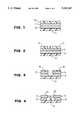
- FIGS. 1, 2, 3, 4, 5, 6, 7 and 8are side sectional views illustrating a sequence of processing steps for forming an in-situ superconductive film on a substrate.
- FIG. 9is a side sectional view of a structure formed by following the steps of FIGS. 1-8.
- a masking structure having a lower layer 10 of niobium and an upper layer 12 of silveris shown as being sandwiched between a substrate 14 and a photoresist layer 16.
- the upper and lower layersmay be deposited by conventional methods known in the art.
- the layersmay be formed by ion beam deposition, sputtering or evaporation.
- the photoresist layeris conventionally formed. Spin-coating of the photoresist is typical.
- the substrate 14is of a type suitable for depositing high T c superconductive films.
- the substratemay be LaAlO 3 , LaGaO 3 , MgO, but other materials may be used.
- the lower layershould have a thickness that exceeds the desired thickness of the high T c film to be formed by approximately 500 nm.
- the upper film 12should have a thickness of approximately 200-300 nm. While the thicknesses are not critical, the thickness of each layer should be constant across the entire substrate.
- the photoresist layer 16is then patterned to form an opening 18, as shown in FIG. 2.
- the method of patterning the photoresistshould be one which provides high resolution, since the opening 18 indirectly dictates dimensions of the high T c film to be formed.
- ion millingis used to transfer the pattern of the photoresist layer 16 through the upper layer 12 of silver.
- the ion millingtypically will penetrate at least a portion of the lower layer 10 as well. The degree of penetration is not important. The result is the structure having a via 20 illustrated in FIG. 3.
- Anisotropic plasma etchingremoves the remainder of the lower layer 10 below the via 20. CF 4 and O 2 are typically used for this purpose. This also removes the photoresist layer. Isotropical etching in the same plasma then etches into the lower layer 10 to form cantilevered portions 22 and 24 in the upper layer 12, as shown in FIG. 4. The area of the second gap 28 as measured parallel to the substrate 14 is greater than the area of the first gap 26.
- the next stepis to deposit the high T c film 30 30 and 32 shown in FIG. 5.
- the film 30 and 32may be YBa 2 Cu 3 O 7 , but this is not critical.
- Deposition of the filmis at an angle perpendicular to the surface of the substrate 14.
- the depositionis an anisotropic deposition. Deposition from varying angles would cover the entire surface of the substrate 14 exposed by etching into the lower layer 10. This is not a desired occurrence. What is preferred is that the formation of the film 32 on the substrate 14 have a length and a width dictated by the patterning of the upper layer 12.
- the structure of FIG. 6is achieved by spin coating a low viscosity solution of polymer 34 onto the device.
- the polymer 34provides a covering, and most importantly seals the high T c film 32 on the substrate 14 from the contact with the ambient atmosphere.
- the polymermay be a material typically used in the art as photoresist. Polyimide may also be used.
- the important characteristic of the sacrificial polymer 34is that it flow readily into the gaps of the upper and lower layers 10 and 12 to completely encapsulate the high T c film 32. Flow phenomena in polymer spin-coating are well known in the art.
- the polymershould have a low molecular weight and be a low viscosity casting solution.
- the fusible and soluble phenol-formaldehyde sold under the trademark Novolac (Baekeland)is suitable.
- the polymeris given a bake sufficient to render it unreactive to acid stripping.
- the bakemay be at a temperature of 180° C. for a period of 60 seconds using a hot plate.
- the bakeis performed after subjecting the polymer to an O 2 plasma for etching of the polymer to a level below the upper extent of the layer 12 of silver. This exposes the high T c film 30 on the upper layer 12 to subsequent processing steps, but a sufficient amount of polymer 34 remains to encapsulate the high T c film 32 on the substrate 14.
- the polymeris shown in FIG. 7 as being etched back below the upper extent of the niobium layer 10, but this is not necessary.
- the upper and lower layers 10 and 12 and the high T c film layer 30 atop the upper layer 12are removed using a suitable acidic etching solution.
- the entire structure illustrated in FIG. 7may be dipped in the solution.
- the acidic solutionis of the type which leaves the polymer 34 intact to provide the structure shown in FIG. 8.
- a solution of 50% concentrated HNO 3 and 5% HF in waterwill remove 1 micron N6 film in approximately two minutes.
- the substrateis reactive to acid, e.g. MgO
- the N6may be removed by CF 4 and O 2 plasma.
- the portion of the high T c film 32 which remainsis that portion sandwiched between the substrate 14 and the polymer 34.
- the polymeris removed by exposing the material to an O 2 plasma.
- the precisely deposited high T c film 32is exposed for subsequent connection to other electrical paths.
- the exposed film 32 on the substrate 14is shown in FIG. 9.
- An advantage of the present inventionis that the high T c film 32 which remains after completion of the process is exposed only to those processing steps of coating of the polymer and removal of the polymer 34. Experiments have shown that this does not affect the in-situ deposited film (as measured by J c and R s ) provided that post-deposition processing steps do not exceed a temperature of approximately 200° C.
- the processis not limited to YBaCuO deposition.
- Other high T c materialsmay be used. Some examples are Bi 2 Sr 2 Ca 1 Cu 2 O 8 , Tl 2 Ca 2 Ba 2 Cu 3 O 10 and (Ba 1-x Rb x )BiO 3 . All of these materials have the characteristics that the materials must be deposited at temperatures too high for conventional lift-off processing to reliably work, and that they contain elements that are not etchable by plasma chemistry and therefore require ion milling in conventional processing.
- Niobiumwas described as the material for formation of the lower layer 10 because niobium is easily etched in a CF 4 /O 2 plasma.
- other materialscan be used, such as tantalum, tungsten, molybdenum and silicon.
- semiconductors, such as siliconwill be defined as metals.
- Use of different materials to form the lower layer 10may require different methods for etching the materials.
- silveris not critical to formation of the upper layer 12. Silver is preferred because it is easily removed by an acidic etch solution, but is inert to the niobium etch and to the YBaCuO deposition conditions. Other materials satisfying these conditions could be used. For example, copper, nickel and gold are good substitutes.
- the purpose of the anisotropical etching to the bottom of the niobium layer 10, as shown in FIG. 3,is to provide a starting point for an isotropic etch that tunnels uniformly under the silver layer 12. If no pre-etching takes place, the isotropic etching will provide a gap in the niobium layer that is larger at its upper extent than at the surface of the substrate 14. However, all of the niobium need not be removed in the anisotropic process step. Typically, the niobium layer is 1 micron thick to achieve a film layer 32 of 0.5 microns. Leaving 100 nm to 300 nm of niobium will achieve satisfactory results. This can be accomplished by the ion milling step, thereby eliminating the need of the anisotropic plasma etch of the niobium.
- Ion milling of the upper layer 12is needed if this layer is a highly inert material, as is desirable to achieve maximum selectivity between the upper layer 12 and the lower layer 10.
- this layeris a highly inert material, as is desirable to achieve maximum selectivity between the upper layer 12 and the lower layer 10.
- silicon or silicon dioxidemay be used as a substitute of silver.
- the present inventionhas the advantage of providing excellent latitude in selection of the steps beyond use of a photoresist patterning that achieves high resolution.
- Conventional lift-off processingrequires delicate control of photoresist exposure and development to obtain a desired undercut profile, and requires careful control of the metal deposition process.
- the cantilevered portions 22 and 24 of the present inventionare provided under conditions of high selectivity, the processing in achieving the desired structure of high T c film and protective capping is not difficult.
- the line width of the high T c filmis determined solely by the width of the gap 26 in the upper layer 12, and not by the undercut of the lower layer 10.
- the processis intrinsically capable of very high resolution, limited only by resist patterning.
- FIGS. 1-9may be achieved by depositing a film of silver as the lower layer 10.
- the filmcould have a thickness of 1 micron, deposited by using an Ar + ion beam deposition system at 1150V, 1 mA/cm 2 beam current at a pressure of 4 ⁇ 10 -4 torr.
- the upper layer 12could then be deposited without breaking vacuum to provide a film of gold having a thickness of 5000 ⁇ .
- a photoresiste.g., AZ5214E photoresist sold by AZ Photoresist Products, could be exposed in a projection aligner and developed to provide a series of openings as small as 5 microns. Such an opening 18 is shown in FIG. 2.
- the initial etch of the lower and upper layers 10 and 12 of silver and goldmay be by use of an Ar + ion beam at 600V, 700 ⁇ A/cm 2 , pressure 4 ⁇ 10 -4 torr, with an angle of incidence of 45° for 47 minutes.
- the undercut 28 in the lower layer 10 of silvermay be formed by etching in a 4:1:1 (by volume) of CH 3 OH:NH 4 OH:H 2 O 2 solution, having an etch rate of approximately 60 ⁇ /sec, for a period of six minutes. The result would be an undercut of approximately 2.5 microns on each side of the gap 26 in the upper layer 12.
- Vacuum pressureplays a role in achieving a desired resolution in depositing the high T c film 32.
- the mean free pathis inversely proportional to pressure.
- in situ YBaCuO deposition processesrun at approximately 5 mtorr for laser ablation, 200-300 mtorr for sputtering, 4 torr for metalorganic chemical vapor deposition and 0.1 mtorr for evaporation.
- system pressureis affected by the manner in which oxygen is introduced.
- Systems that use oxygen excited by an electron cyclotron resonance plasma sourcecan run at lower pressures.
- the inventionmay be used with a considerable range of deposition systems. No one method has been determined to yield films of higher quality than the others.
- the polymer 34may be spun to a thickness of 1.5 microns and then etched back to expose the upper layer 12 of gold, while still covering the superconductive film 32 on the substrate 14, by using an O 2 plasma at 240 mtorr, 100W rf power for a period of thirty minutes.
- the gold 12may be removed by a KI/I 2 solution (4 g KI, 1 g I 2 in 4 ml water) and the silver 10 may be removed by mild acid, e.g., 10% HNO 3 .
- the O 2 plasmamay be reapplied to remove the remainder of the polymer 34.
Landscapes
- Chemical & Material Sciences (AREA)
- Engineering & Computer Science (AREA)
- Ceramic Engineering (AREA)
- Materials Engineering (AREA)
- Structural Engineering (AREA)
- Organic Chemistry (AREA)
- Manufacturing & Machinery (AREA)
- Superconductor Devices And Manufacturing Methods Thereof (AREA)
Abstract
Description
Claims (16)
Priority Applications (1)
| Application Number | Priority Date | Filing Date | Title |
|---|---|---|---|
| US07/700,671US5212147A (en) | 1991-05-15 | 1991-05-15 | Method of forming a patterned in-situ high Tc superconductive film |
Applications Claiming Priority (1)
| Application Number | Priority Date | Filing Date | Title |
|---|---|---|---|
| US07/700,671US5212147A (en) | 1991-05-15 | 1991-05-15 | Method of forming a patterned in-situ high Tc superconductive film |
Publications (1)
| Publication Number | Publication Date |
|---|---|
| US5212147Atrue US5212147A (en) | 1993-05-18 |
Family
ID=24814439
Family Applications (1)
| Application Number | Title | Priority Date | Filing Date |
|---|---|---|---|
| US07/700,671Expired - LifetimeUS5212147A (en) | 1991-05-15 | 1991-05-15 | Method of forming a patterned in-situ high Tc superconductive film |
Country Status (1)
| Country | Link |
|---|---|
| US (1) | US5212147A (en) |
Cited By (56)
| Publication number | Priority date | Publication date | Assignee | Title |
|---|---|---|---|---|
| US20020094496A1 (en)* | 2000-07-17 | 2002-07-18 | Choi Byung J. | Method and system of automatic fluid dispensing for imprint lithography processes |
| US20020093122A1 (en)* | 2000-08-01 | 2002-07-18 | Choi Byung J. | Methods for high-precision gap and orientation sensing between a transparent template and substrate for imprint lithography |
| US20020150398A1 (en)* | 2000-08-21 | 2002-10-17 | Choi Byung J. | Flexure based macro motion translation stage |
| US6576152B2 (en)* | 2000-07-06 | 2003-06-10 | Matsushita Electric Industrial Co., Ltd. | Dry etching method |
| US20030205657A1 (en)* | 2002-05-01 | 2003-11-06 | Voisin Ronald D. | Methods of manufacturing a lithography template |
| US20030215577A1 (en)* | 2002-05-16 | 2003-11-20 | Willson Carlton Grant | Method and system for fabricating nanoscale patterns in light curable compositions using an electric field |
| US20030235787A1 (en)* | 2002-06-24 | 2003-12-25 | Watts Michael P.C. | Low viscosity high resolution patterning material |
| US20040009673A1 (en)* | 2002-07-11 | 2004-01-15 | Sreenivasan Sidlgata V. | Method and system for imprint lithography using an electric field |
| US6686128B1 (en)* | 2001-08-17 | 2004-02-03 | Tfr Technologies, Inc. | Method of fabricating patterned layers of material upon a substrate |
| US20040022888A1 (en)* | 2002-08-01 | 2004-02-05 | Sreenivasan Sidlgata V. | Alignment systems for imprint lithography |
| US20040038552A1 (en)* | 2002-08-23 | 2004-02-26 | Watts Michael P.C. | Method for fabricating bulbous-shaped vias |
| US20040053146A1 (en)* | 2000-07-16 | 2004-03-18 | University Of Texas System Board Of Regents, Ut System | Method of varying template dimensions to achieve alignment during imprint lithography |
| US20040089979A1 (en)* | 2002-11-13 | 2004-05-13 | Molecular Imprints, Inc. | Method of reducing pattern distortions during imprint lithography processes |
| US20040104641A1 (en)* | 1999-10-29 | 2004-06-03 | University Of Texas System | Method of separating a template from a substrate during imprint lithography |
| US20040112861A1 (en)* | 2002-12-11 | 2004-06-17 | Molecular Imprints, Inc. | Method for modulating shapes of substrates |
| US20040112153A1 (en)* | 2002-12-12 | 2004-06-17 | Molecular Imprints, Inc. | Method and system for determining characteristics of substrates employing fluid geometries |
| US20040124566A1 (en)* | 2002-07-11 | 2004-07-01 | Sreenivasan Sidlgata V. | Step and repeat imprint lithography processes |
| US20040166749A1 (en)* | 2003-02-21 | 2004-08-26 | Le Gette Brian Edward | Collapsible flotation device having support member |
| US20040170771A1 (en)* | 2000-10-12 | 2004-09-02 | Board Of Regents, The University Of Texas System | Method of creating a dispersion of a liquid on a substrate |
| US20040170770A1 (en)* | 2003-02-27 | 2004-09-02 | Molecular Imprints, Inc. | Method to reduce adhesion between a polymerizable layer and a substrate employing a fluorine-containing layer |
| US20040188381A1 (en)* | 2003-03-25 | 2004-09-30 | Molecular Imprints, Inc. | Positive tone bi-layer imprint lithography method |
| US20040211754A1 (en)* | 2003-04-25 | 2004-10-28 | Molecular Imprints, Inc. | Method of forming stepped structures employing imprint lithography |
| US20050072755A1 (en)* | 2003-10-02 | 2005-04-07 | University Of Texas System Board Of Regents | Single phase fluid imprint lithography method |
| US20050084804A1 (en)* | 2003-10-16 | 2005-04-21 | Molecular Imprints, Inc. | Low surface energy templates |
| US6900881B2 (en) | 2002-07-11 | 2005-05-31 | Molecular Imprints, Inc. | Step and repeat imprint lithography systems |
| US6916584B2 (en) | 2002-08-01 | 2005-07-12 | Molecular Imprints, Inc. | Alignment methods for imprint lithography |
| US6926929B2 (en) | 2002-07-09 | 2005-08-09 | Molecular Imprints, Inc. | System and method for dispensing liquids |
| US6932934B2 (en) | 2002-07-11 | 2005-08-23 | Molecular Imprints, Inc. | Formation of discontinuous films during an imprint lithography process |
| US20050275311A1 (en)* | 2004-06-01 | 2005-12-15 | Molecular Imprints, Inc. | Compliant device for nano-scale manufacturing |
| US20050274219A1 (en)* | 2004-06-01 | 2005-12-15 | Molecular Imprints, Inc. | Method and system to control movement of a body for nano-scale manufacturing |
| US7019819B2 (en) | 2002-11-13 | 2006-03-28 | Molecular Imprints, Inc. | Chucking system for modulating shapes of substrates |
| US7027156B2 (en) | 2002-08-01 | 2006-04-11 | Molecular Imprints, Inc. | Scatterometry alignment for imprint lithography |
| US20060145398A1 (en)* | 2004-12-30 | 2006-07-06 | Board Of Regents, The University Of Texas System | Release layer comprising diamond-like carbon (DLC) or doped DLC with tunable composition for imprint lithography templates and contact masks |
| US7122079B2 (en) | 2004-02-27 | 2006-10-17 | Molecular Imprints, Inc. | Composition for an etching mask comprising a silicon-containing material |
| US7136150B2 (en) | 2003-09-25 | 2006-11-14 | Molecular Imprints, Inc. | Imprint lithography template having opaque alignment marks |
| US7157036B2 (en) | 2003-06-17 | 2007-01-02 | Molecular Imprints, Inc | Method to reduce adhesion between a conformable region and a pattern of a mold |
| US20070126150A1 (en)* | 2005-12-01 | 2007-06-07 | Molecular Imprints, Inc. | Bifurcated contact printing technique |
| US20070126156A1 (en)* | 2005-12-01 | 2007-06-07 | Molecular Imprints, Inc. | Technique for separating a mold from solidified imprinting material |
| US20070132152A1 (en)* | 2005-12-08 | 2007-06-14 | Molecular Imprints, Inc. | Method and System for Double-Sided Patterning of Substrates |
| US20070170617A1 (en)* | 2006-01-20 | 2007-07-26 | Molecular Imprints, Inc. | Patterning Substrates Employing Multiple Chucks |
| US20070228610A1 (en)* | 2006-04-03 | 2007-10-04 | Molecular Imprints, Inc. | Method of Concurrently Patterning a Substrate Having a Plurality of Fields and a Plurality of Alignment Marks |
| US20070243655A1 (en)* | 2006-04-18 | 2007-10-18 | Molecular Imprints, Inc. | Self-Aligned Process for Fabricating Imprint Templates Containing Variously Etched Features |
| US20080141862A1 (en)* | 2003-10-02 | 2008-06-19 | Molecular Imprints, Inc. | Single Phase Fluid Imprint Lithography Method |
| US20090250840A1 (en)* | 2006-04-18 | 2009-10-08 | Molecular Imprints, Inc. | Template Having Alignment Marks Formed of Contrast Material |
| US7802978B2 (en) | 2006-04-03 | 2010-09-28 | Molecular Imprints, Inc. | Imprinting of partial fields at the edge of the wafer |
| US7906180B2 (en) | 2004-02-27 | 2011-03-15 | Molecular Imprints, Inc. | Composition for an etching mask comprising a silicon-containing material |
| US8076386B2 (en) | 2004-02-23 | 2011-12-13 | Molecular Imprints, Inc. | Materials for imprint lithography |
| US8142850B2 (en) | 2006-04-03 | 2012-03-27 | Molecular Imprints, Inc. | Patterning a plurality of fields on a substrate to compensate for differing evaporation times |
| US8349241B2 (en) | 2002-10-04 | 2013-01-08 | Molecular Imprints, Inc. | Method to arrange features on a substrate to replicate features having minimal dimensional variability |
| US8850980B2 (en) | 2006-04-03 | 2014-10-07 | Canon Nanotechnologies, Inc. | Tessellated patterns in imprint lithography |
| CN104396038A (en)* | 2012-05-21 | 2015-03-04 | 丹麦技术大学 | Method for producing substrates for superconducting layers |
| US9177814B2 (en) | 2013-03-15 | 2015-11-03 | International Business Machines Corporation | Suspended superconducting qubits |
| CN105794007A (en)* | 2013-11-20 | 2016-07-20 | 丹麦科技大学 | Method for manufacturing a substrate for a superconducting layer |
| US9515247B1 (en) | 2015-05-18 | 2016-12-06 | International Business Machines Corporation | Sacrificial shorting straps for superconducting qubits |
| US9614270B2 (en) | 2015-04-30 | 2017-04-04 | International Business Machines Corporation | Superconducting airbridge crossover using superconducting sacrificial material |
| CN113380942A (en)* | 2021-05-31 | 2021-09-10 | 中国科学院微电子研究所 | Preparation method of Josephson junction and Josephson junction |
Citations (10)
| Publication number | Priority date | Publication date | Assignee | Title |
|---|---|---|---|---|
| US3975252A (en)* | 1975-03-14 | 1976-08-17 | Bell Telephone Laboratories, Incorporated | High-resolution sputter etching |
| US4650543A (en)* | 1984-03-02 | 1987-03-17 | Kabushiki Kaisha Toshiba | Method of forming electrode pattern of semiconductor device |
| US4742026A (en)* | 1986-04-30 | 1988-05-03 | Thomson-Csf | Method for the selective dry etching of layers of III-V group semiconductive materials |
| US4764245A (en)* | 1986-05-07 | 1988-08-16 | Siemens Aktiengesellschaft | Method for generating contact holes with beveled sidewalls in intermediate oxide layers |
| US4882312A (en)* | 1988-05-09 | 1989-11-21 | General Electric Company | Evaporation of high Tc Y-Ba-Cu-O superconducting thin film on Si and SiO2 with a zirconia buffer layer |
| US4933318A (en)* | 1987-12-16 | 1990-06-12 | U.S. Philips Corporation | Plasma etch of masked superconductor film |
| US4937225A (en)* | 1987-07-10 | 1990-06-26 | Massachusetts Institute Of Technology | Rapid solidification processing of oxide superconductors |
| US4942142A (en)* | 1987-07-27 | 1990-07-17 | Sumitomo Electric Industries Ltd. | Superconducting thin film and a method for preparing the same |
| US4952557A (en)* | 1987-11-09 | 1990-08-28 | Ametek, Inc. | Formation of superconducting articles by electrodeposition |
| US4952556A (en)* | 1987-12-08 | 1990-08-28 | General Motors Corporation | Patterning thin film superconductors using focused beam techniques |
- 1991
- 1991-05-15USUS07/700,671patent/US5212147A/ennot_activeExpired - Lifetime
Patent Citations (10)
| Publication number | Priority date | Publication date | Assignee | Title |
|---|---|---|---|---|
| US3975252A (en)* | 1975-03-14 | 1976-08-17 | Bell Telephone Laboratories, Incorporated | High-resolution sputter etching |
| US4650543A (en)* | 1984-03-02 | 1987-03-17 | Kabushiki Kaisha Toshiba | Method of forming electrode pattern of semiconductor device |
| US4742026A (en)* | 1986-04-30 | 1988-05-03 | Thomson-Csf | Method for the selective dry etching of layers of III-V group semiconductive materials |
| US4764245A (en)* | 1986-05-07 | 1988-08-16 | Siemens Aktiengesellschaft | Method for generating contact holes with beveled sidewalls in intermediate oxide layers |
| US4937225A (en)* | 1987-07-10 | 1990-06-26 | Massachusetts Institute Of Technology | Rapid solidification processing of oxide superconductors |
| US4942142A (en)* | 1987-07-27 | 1990-07-17 | Sumitomo Electric Industries Ltd. | Superconducting thin film and a method for preparing the same |
| US4952557A (en)* | 1987-11-09 | 1990-08-28 | Ametek, Inc. | Formation of superconducting articles by electrodeposition |
| US4952556A (en)* | 1987-12-08 | 1990-08-28 | General Motors Corporation | Patterning thin film superconductors using focused beam techniques |
| US4933318A (en)* | 1987-12-16 | 1990-06-12 | U.S. Philips Corporation | Plasma etch of masked superconductor film |
| US4882312A (en)* | 1988-05-09 | 1989-11-21 | General Electric Company | Evaporation of high Tc Y-Ba-Cu-O superconducting thin film on Si and SiO2 with a zirconia buffer layer |
Cited By (102)
| Publication number | Priority date | Publication date | Assignee | Title |
|---|---|---|---|---|
| US20040104641A1 (en)* | 1999-10-29 | 2004-06-03 | University Of Texas System | Method of separating a template from a substrate during imprint lithography |
| US7060402B2 (en) | 1999-10-29 | 2006-06-13 | Board Of Regents, The University Of Texas System | Method of orientating a template with respect to a substrate in response to a force exerted on the template |
| US6955868B2 (en) | 1999-10-29 | 2005-10-18 | Board Of Regents, The University Of Texas System | Method to control the relative position between a body and a surface |
| US20050089774A1 (en)* | 1999-10-29 | 2005-04-28 | Board Of Regents, The University Of Texas System | Method to control the relative position between a body and a surface |
| US7098572B2 (en) | 1999-10-29 | 2006-08-29 | Board Of Regents, The University Of Texas System | Apparatus to control displacement of a body spaced-apart from a surface |
| US6873087B1 (en) | 1999-10-29 | 2005-03-29 | Board Of Regents, The University Of Texas System | High precision orientation alignment and gap control stages for imprint lithography processes |
| US20040168588A1 (en)* | 1999-10-29 | 2004-09-02 | Board Of Regents, The University Of Texas System | Method of orientating a template with respect to a substrate in response to a force exerted on the template |
| US6576152B2 (en)* | 2000-07-06 | 2003-06-10 | Matsushita Electric Industrial Co., Ltd. | Dry etching method |
| US20040209177A1 (en)* | 2000-07-16 | 2004-10-21 | Board Of Regents, The University Of Texas System | Dual wavelength method of determining a relative position of a substrate and a template |
| US20040189996A1 (en)* | 2000-07-16 | 2004-09-30 | Board Of Regents, The University Of Texas System | Method of aligning a template with a substrate employing moire patterns |
| US20040053146A1 (en)* | 2000-07-16 | 2004-03-18 | University Of Texas System Board Of Regents, Ut System | Method of varying template dimensions to achieve alignment during imprint lithography |
| US6986975B2 (en) | 2000-07-16 | 2006-01-17 | Board Of Regents, The University Of Texas System | Method of aligning a template with a substrate employing moire patterns |
| US6921615B2 (en) | 2000-07-16 | 2005-07-26 | Board Of Regents, The University Of Texas System | High-resolution overlay alignment methods for imprint lithography |
| US6916585B2 (en) | 2000-07-16 | 2005-07-12 | Board Of Regents, The University Of Texas Systems | Method of varying template dimensions to achieve alignment during imprint lithography |
| US6902853B2 (en) | 2000-07-16 | 2005-06-07 | Board Of Regents, The University Of Texas System | Dual wavelength method of determining a relative position of a substrate and a template |
| US9223202B2 (en) | 2000-07-17 | 2015-12-29 | Board Of Regents, The University Of Texas System | Method of automatic fluid dispensing for imprint lithography processes |
| US20020094496A1 (en)* | 2000-07-17 | 2002-07-18 | Choi Byung J. | Method and system of automatic fluid dispensing for imprint lithography processes |
| US20020093122A1 (en)* | 2000-08-01 | 2002-07-18 | Choi Byung J. | Methods for high-precision gap and orientation sensing between a transparent template and substrate for imprint lithography |
| US6954275B2 (en) | 2000-08-01 | 2005-10-11 | Boards Of Regents, The University Of Texas System | Methods for high-precision gap and orientation sensing between a transparent template and substrate for imprint lithography |
| US20020150398A1 (en)* | 2000-08-21 | 2002-10-17 | Choi Byung J. | Flexure based macro motion translation stage |
| US8016277B2 (en) | 2000-08-21 | 2011-09-13 | Board Of Regents, The University Of Texas System | Flexure based macro motion translation stage |
| US20040170771A1 (en)* | 2000-10-12 | 2004-09-02 | Board Of Regents, The University Of Texas System | Method of creating a dispersion of a liquid on a substrate |
| US7060324B2 (en) | 2000-10-12 | 2006-06-13 | Board Of Regents, The University Of Texas System | Method of creating a dispersion of a liquid on a substrate |
| US6686128B1 (en)* | 2001-08-17 | 2004-02-03 | Tfr Technologies, Inc. | Method of fabricating patterned layers of material upon a substrate |
| US20030205657A1 (en)* | 2002-05-01 | 2003-11-06 | Voisin Ronald D. | Methods of manufacturing a lithography template |
| US7037639B2 (en) | 2002-05-01 | 2006-05-02 | Molecular Imprints, Inc. | Methods of manufacturing a lithography template |
| US6964793B2 (en) | 2002-05-16 | 2005-11-15 | Board Of Regents, The University Of Texas System | Method for fabricating nanoscale patterns in light curable compositions using an electric field |
| US20030215577A1 (en)* | 2002-05-16 | 2003-11-20 | Willson Carlton Grant | Method and system for fabricating nanoscale patterns in light curable compositions using an electric field |
| US20030235787A1 (en)* | 2002-06-24 | 2003-12-25 | Watts Michael P.C. | Low viscosity high resolution patterning material |
| US6926929B2 (en) | 2002-07-09 | 2005-08-09 | Molecular Imprints, Inc. | System and method for dispensing liquids |
| US7077992B2 (en) | 2002-07-11 | 2006-07-18 | Molecular Imprints, Inc. | Step and repeat imprint lithography processes |
| US20040009673A1 (en)* | 2002-07-11 | 2004-01-15 | Sreenivasan Sidlgata V. | Method and system for imprint lithography using an electric field |
| US6908861B2 (en) | 2002-07-11 | 2005-06-21 | Molecular Imprints, Inc. | Method for imprint lithography using an electric field |
| US7338275B2 (en) | 2002-07-11 | 2008-03-04 | Molecular Imprints, Inc. | Formation of discontinuous films during an imprint lithography process |
| US6900881B2 (en) | 2002-07-11 | 2005-05-31 | Molecular Imprints, Inc. | Step and repeat imprint lithography systems |
| US20040124566A1 (en)* | 2002-07-11 | 2004-07-01 | Sreenivasan Sidlgata V. | Step and repeat imprint lithography processes |
| US7727453B2 (en) | 2002-07-11 | 2010-06-01 | Molecular Imprints, Inc. | Step and repeat imprint lithography processes |
| US6932934B2 (en) | 2002-07-11 | 2005-08-23 | Molecular Imprints, Inc. | Formation of discontinuous films during an imprint lithography process |
| US7070405B2 (en) | 2002-08-01 | 2006-07-04 | Molecular Imprints, Inc. | Alignment systems for imprint lithography |
| US20040022888A1 (en)* | 2002-08-01 | 2004-02-05 | Sreenivasan Sidlgata V. | Alignment systems for imprint lithography |
| US7027156B2 (en) | 2002-08-01 | 2006-04-11 | Molecular Imprints, Inc. | Scatterometry alignment for imprint lithography |
| US6916584B2 (en) | 2002-08-01 | 2005-07-12 | Molecular Imprints, Inc. | Alignment methods for imprint lithography |
| US7071088B2 (en) | 2002-08-23 | 2006-07-04 | Molecular Imprints, Inc. | Method for fabricating bulbous-shaped vias |
| US20040038552A1 (en)* | 2002-08-23 | 2004-02-26 | Watts Michael P.C. | Method for fabricating bulbous-shaped vias |
| US8349241B2 (en) | 2002-10-04 | 2013-01-08 | Molecular Imprints, Inc. | Method to arrange features on a substrate to replicate features having minimal dimensional variability |
| US6929762B2 (en) | 2002-11-13 | 2005-08-16 | Molecular Imprints, Inc. | Method of reducing pattern distortions during imprint lithography processes |
| US20040089979A1 (en)* | 2002-11-13 | 2004-05-13 | Molecular Imprints, Inc. | Method of reducing pattern distortions during imprint lithography processes |
| US7019819B2 (en) | 2002-11-13 | 2006-03-28 | Molecular Imprints, Inc. | Chucking system for modulating shapes of substrates |
| US20040112861A1 (en)* | 2002-12-11 | 2004-06-17 | Molecular Imprints, Inc. | Method for modulating shapes of substrates |
| US6980282B2 (en) | 2002-12-11 | 2005-12-27 | Molecular Imprints, Inc. | Method for modulating shapes of substrates |
| US6871558B2 (en) | 2002-12-12 | 2005-03-29 | Molecular Imprints, Inc. | Method for determining characteristics of substrate employing fluid geometries |
| US20040112153A1 (en)* | 2002-12-12 | 2004-06-17 | Molecular Imprints, Inc. | Method and system for determining characteristics of substrates employing fluid geometries |
| US20040166749A1 (en)* | 2003-02-21 | 2004-08-26 | Le Gette Brian Edward | Collapsible flotation device having support member |
| US20040170770A1 (en)* | 2003-02-27 | 2004-09-02 | Molecular Imprints, Inc. | Method to reduce adhesion between a polymerizable layer and a substrate employing a fluorine-containing layer |
| US7452574B2 (en) | 2003-02-27 | 2008-11-18 | Molecular Imprints, Inc. | Method to reduce adhesion between a polymerizable layer and a substrate employing a fluorine-containing layer |
| US7179396B2 (en) | 2003-03-25 | 2007-02-20 | Molecular Imprints, Inc. | Positive tone bi-layer imprint lithography method |
| US20040188381A1 (en)* | 2003-03-25 | 2004-09-30 | Molecular Imprints, Inc. | Positive tone bi-layer imprint lithography method |
| US7396475B2 (en) | 2003-04-25 | 2008-07-08 | Molecular Imprints, Inc. | Method of forming stepped structures employing imprint lithography |
| US20040211754A1 (en)* | 2003-04-25 | 2004-10-28 | Molecular Imprints, Inc. | Method of forming stepped structures employing imprint lithography |
| US7157036B2 (en) | 2003-06-17 | 2007-01-02 | Molecular Imprints, Inc | Method to reduce adhesion between a conformable region and a pattern of a mold |
| US7136150B2 (en) | 2003-09-25 | 2006-11-14 | Molecular Imprints, Inc. | Imprint lithography template having opaque alignment marks |
| US20080141862A1 (en)* | 2003-10-02 | 2008-06-19 | Molecular Imprints, Inc. | Single Phase Fluid Imprint Lithography Method |
| US20050072755A1 (en)* | 2003-10-02 | 2005-04-07 | University Of Texas System Board Of Regents | Single phase fluid imprint lithography method |
| US7090716B2 (en) | 2003-10-02 | 2006-08-15 | Molecular Imprints, Inc. | Single phase fluid imprint lithography method |
| US8211214B2 (en) | 2003-10-02 | 2012-07-03 | Molecular Imprints, Inc. | Single phase fluid imprint lithography method |
| US20050084804A1 (en)* | 2003-10-16 | 2005-04-21 | Molecular Imprints, Inc. | Low surface energy templates |
| US8076386B2 (en) | 2004-02-23 | 2011-12-13 | Molecular Imprints, Inc. | Materials for imprint lithography |
| US7122079B2 (en) | 2004-02-27 | 2006-10-17 | Molecular Imprints, Inc. | Composition for an etching mask comprising a silicon-containing material |
| US7906180B2 (en) | 2004-02-27 | 2011-03-15 | Molecular Imprints, Inc. | Composition for an etching mask comprising a silicon-containing material |
| US20050274219A1 (en)* | 2004-06-01 | 2005-12-15 | Molecular Imprints, Inc. | Method and system to control movement of a body for nano-scale manufacturing |
| US20050275311A1 (en)* | 2004-06-01 | 2005-12-15 | Molecular Imprints, Inc. | Compliant device for nano-scale manufacturing |
| US20060145398A1 (en)* | 2004-12-30 | 2006-07-06 | Board Of Regents, The University Of Texas System | Release layer comprising diamond-like carbon (DLC) or doped DLC with tunable composition for imprint lithography templates and contact masks |
| US20070126156A1 (en)* | 2005-12-01 | 2007-06-07 | Molecular Imprints, Inc. | Technique for separating a mold from solidified imprinting material |
| US20070126150A1 (en)* | 2005-12-01 | 2007-06-07 | Molecular Imprints, Inc. | Bifurcated contact printing technique |
| US7803308B2 (en) | 2005-12-01 | 2010-09-28 | Molecular Imprints, Inc. | Technique for separating a mold from solidified imprinting material |
| US7906058B2 (en) | 2005-12-01 | 2011-03-15 | Molecular Imprints, Inc. | Bifurcated contact printing technique |
| US7670529B2 (en) | 2005-12-08 | 2010-03-02 | Molecular Imprints, Inc. | Method and system for double-sided patterning of substrates |
| US20070132152A1 (en)* | 2005-12-08 | 2007-06-14 | Molecular Imprints, Inc. | Method and System for Double-Sided Patterning of Substrates |
| US7670530B2 (en) | 2006-01-20 | 2010-03-02 | Molecular Imprints, Inc. | Patterning substrates employing multiple chucks |
| US20070170617A1 (en)* | 2006-01-20 | 2007-07-26 | Molecular Imprints, Inc. | Patterning Substrates Employing Multiple Chucks |
| US7802978B2 (en) | 2006-04-03 | 2010-09-28 | Molecular Imprints, Inc. | Imprinting of partial fields at the edge of the wafer |
| US8142850B2 (en) | 2006-04-03 | 2012-03-27 | Molecular Imprints, Inc. | Patterning a plurality of fields on a substrate to compensate for differing evaporation times |
| US20070228610A1 (en)* | 2006-04-03 | 2007-10-04 | Molecular Imprints, Inc. | Method of Concurrently Patterning a Substrate Having a Plurality of Fields and a Plurality of Alignment Marks |
| US8850980B2 (en) | 2006-04-03 | 2014-10-07 | Canon Nanotechnologies, Inc. | Tessellated patterns in imprint lithography |
| US7780893B2 (en) | 2006-04-03 | 2010-08-24 | Molecular Imprints, Inc. | Method of concurrently patterning a substrate having a plurality of fields and a plurality of alignment marks |
| US20090250840A1 (en)* | 2006-04-18 | 2009-10-08 | Molecular Imprints, Inc. | Template Having Alignment Marks Formed of Contrast Material |
| US8012395B2 (en) | 2006-04-18 | 2011-09-06 | Molecular Imprints, Inc. | Template having alignment marks formed of contrast material |
| US7547398B2 (en) | 2006-04-18 | 2009-06-16 | Molecular Imprints, Inc. | Self-aligned process for fabricating imprint templates containing variously etched features |
| US20070243655A1 (en)* | 2006-04-18 | 2007-10-18 | Molecular Imprints, Inc. | Self-Aligned Process for Fabricating Imprint Templates Containing Variously Etched Features |
| RU2626052C2 (en)* | 2012-05-21 | 2017-07-21 | Датский Технический Университет | Method for obtaining substrates for superconducting layers |
| US9496477B2 (en) | 2012-05-21 | 2016-11-15 | Danmarks Tekniske Universitet | Method for producing substrates for superconducting layers |
| CN104396038A (en)* | 2012-05-21 | 2015-03-04 | 丹麦技术大学 | Method for producing substrates for superconducting layers |
| CN104396038B (en)* | 2012-05-21 | 2017-12-15 | 丹麦技术大学 | Method for producing the substrate for superconducting layer |
| US9177814B2 (en) | 2013-03-15 | 2015-11-03 | International Business Machines Corporation | Suspended superconducting qubits |
| US9716219B2 (en) | 2013-03-15 | 2017-07-25 | International Business Machines Corporation | Suspended superconducting qubits |
| US10008655B2 (en) | 2013-03-15 | 2018-06-26 | International Business Machines Corporation | Suspended superconducting qubits |
| CN105794007A (en)* | 2013-11-20 | 2016-07-20 | 丹麦科技大学 | Method for manufacturing a substrate for a superconducting layer |
| US9614270B2 (en) | 2015-04-30 | 2017-04-04 | International Business Machines Corporation | Superconducting airbridge crossover using superconducting sacrificial material |
| US11380974B2 (en) | 2015-04-30 | 2022-07-05 | International Business Machines Corporation | Superconducting airbridge crossover using superconducting sacrificial material |
| US9515247B1 (en) | 2015-05-18 | 2016-12-06 | International Business Machines Corporation | Sacrificial shorting straps for superconducting qubits |
| CN113380942A (en)* | 2021-05-31 | 2021-09-10 | 中国科学院微电子研究所 | Preparation method of Josephson junction and Josephson junction |
| CN113380942B (en)* | 2021-05-31 | 2022-09-16 | 中国科学院微电子研究所 | Preparation method of Josephson junction and Josephson junction |
Similar Documents
| Publication | Publication Date | Title |
|---|---|---|
| US5212147A (en) | Method of forming a patterned in-situ high Tc superconductive film | |
| KR100490575B1 (en) | Method of forming noble metal thin film pattern | |
| US5256636A (en) | Microelectronic superconducting device with multi-layer contact | |
| US5348617A (en) | Selective etching process | |
| EP0024571A2 (en) | Selective metal removal in the presence of a metal silicide | |
| US6156672A (en) | Method of forming dielectric thin film pattern and method of forming laminate pattern comprising dielectric thin film and conductive thin film | |
| JPS5828736B2 (en) | How to form a flat thin film | |
| US4029562A (en) | Forming feedthrough connections for multi-level interconnections metallurgy systems | |
| US4933318A (en) | Plasma etch of masked superconductor film | |
| US4214966A (en) | Process useful in the fabrication of articles with metallized surfaces | |
| US4548834A (en) | Method of producing a Josephson tunnel barrier | |
| EP0219465B1 (en) | Improved (rie) plasma etch process for making metal-semiconductor ohmic type contacts | |
| US4299679A (en) | Method of producing Josephson elements of the tunneling junction type | |
| EP0076215B1 (en) | Lift-off shadow mask | |
| US3984300A (en) | Semiconductor pattern delineation by sputter etching process | |
| US4409262A (en) | Fabrication of submicron-wide lines with shadow depositions | |
| US5650377A (en) | Selective epitaxial growth of high-TC superconductive material | |
| EP0090612B1 (en) | Method of making josephson junction devices | |
| JPS5978585A (en) | Josephson integrated circuit | |
| JP2682136B2 (en) | Method of manufacturing Josephson device | |
| USRE29947E (en) | Semiconductor pattern delineation by sputter etching process | |
| JP2691175B2 (en) | Patterned oxide superconducting film formation method | |
| JPS58209183A (en) | Manufacture of josephson junction element | |
| Salmi et al. | Thin film process for Nb/NbOx/(Pb-In-Au) Josephson junction devices | |
| JPS6143488A (en) | Method for manufacturing superconducting contacts |
Legal Events
| Date | Code | Title | Description |
|---|---|---|---|
| AS | Assignment | Owner name:HEWLETT-PACKARD COMPANY, A CORPORATION OF CA, CALI Free format text:ASSIGNMENT OF ASSIGNORS INTEREST.;ASSIGNOR:SHEATS, JAMES R.;REEL/FRAME:006236/0964 Effective date:19910513 | |
| STCF | Information on status: patent grant | Free format text:PATENTED CASE | |
| CC | Certificate of correction | ||
| FEPP | Fee payment procedure | Free format text:PAYOR NUMBER ASSIGNED (ORIGINAL EVENT CODE: ASPN); ENTITY STATUS OF PATENT OWNER: LARGE ENTITY | |
| FPAY | Fee payment | Year of fee payment:4 | |
| AS | Assignment | Owner name:HEWLETT-PACKARD COMPANY, A DELAWARE CORPORATION, C Free format text:MERGER;ASSIGNOR:HEWLETT-PACKARD COMPANY, A CALIFORNIA CORPORATION;REEL/FRAME:010841/0649 Effective date:19980520 | |
| AS | Assignment | Owner name:AGILENT TECHNOLOGIES INC., CALIFORNIA Free format text:ASSIGNMENT OF ASSIGNORS INTEREST;ASSIGNOR:HEWLETT-PACKARD COMPANY, A DELAWARE CORPORATION;REEL/FRAME:010901/0336 Effective date:20000520 | |
| FPAY | Fee payment | Year of fee payment:8 | |
| FPAY | Fee payment | Year of fee payment:12 |