US5208961A - Semiconductor processing furnace door alignment apparatus and method - Google Patents
Semiconductor processing furnace door alignment apparatus and methodDownload PDFInfo
- Publication number
- US5208961A US5208961AUS07/843,537US84353792AUS5208961AUS 5208961 AUS5208961 AUS 5208961AUS 84353792 AUS84353792 AUS 84353792AUS 5208961 AUS5208961 AUS 5208961A
- Authority
- US
- United States
- Prior art keywords
- alignment
- furnace
- door
- furnace door
- bore
- Prior art date
- Legal status (The legal status is an assumption and is not a legal conclusion. Google has not performed a legal analysis and makes no representation as to the accuracy of the status listed.)
- Expired - Lifetime
Links
- 238000000034methodMethods0.000titleclaimsdescription20
- 239000004065semiconductorSubstances0.000titledescription11
- 238000007789sealingMethods0.000claimsdescription6
- XLYOFNOQVPJJNP-UHFFFAOYSA-NwaterSubstancesOXLYOFNOQVPJJNP-UHFFFAOYSA-N0.000claims1
- 235000012431wafersNutrition0.000description38
- 239000010453quartzSubstances0.000description24
- VYPSYNLAJGMNEJ-UHFFFAOYSA-Nsilicon dioxideInorganic materialsO=[Si]=OVYPSYNLAJGMNEJ-UHFFFAOYSA-N0.000description24
- 235000009508confectioneryNutrition0.000description7
- 125000006850spacer groupChemical group0.000description5
- 230000008569processEffects0.000description4
- 238000005229chemical vapour depositionMethods0.000description3
- 239000007789gasSubstances0.000description3
- 239000000463materialSubstances0.000description3
- 230000004323axial lengthEffects0.000description2
- 238000000151depositionMethods0.000description2
- 238000006073displacement reactionMethods0.000description2
- 239000000203mixtureSubstances0.000description2
- 239000000126substanceSubstances0.000description2
- 229910000619316 stainless steelInorganic materials0.000description1
- 230000009471actionEffects0.000description1
- 230000006835compressionEffects0.000description1
- 238000007906compressionMethods0.000description1
- 230000008878couplingEffects0.000description1
- 238000010168coupling processMethods0.000description1
- 238000005859coupling reactionMethods0.000description1
- 230000001419dependent effectEffects0.000description1
- 238000009792diffusion processMethods0.000description1
- 238000009826distributionMethods0.000description1
- 239000002019doping agentSubstances0.000description1
- 238000003780insertionMethods0.000description1
- 230000037431insertionEffects0.000description1
- 238000004519manufacturing processMethods0.000description1
- 239000002184metalSubstances0.000description1
- HBMJWWWQQXIZIP-UHFFFAOYSA-Nsilicon carbideChemical compound[Si+]#[C-]HBMJWWWQQXIZIP-UHFFFAOYSA-N0.000description1
- 229910010271silicon carbideInorganic materials0.000description1
- 239000000758substrateSubstances0.000description1
Images
Classifications
- C—CHEMISTRY; METALLURGY
- C30—CRYSTAL GROWTH
- C30B—SINGLE-CRYSTAL GROWTH; UNIDIRECTIONAL SOLIDIFICATION OF EUTECTIC MATERIAL OR UNIDIRECTIONAL DEMIXING OF EUTECTOID MATERIAL; REFINING BY ZONE-MELTING OF MATERIAL; PRODUCTION OF A HOMOGENEOUS POLYCRYSTALLINE MATERIAL WITH DEFINED STRUCTURE; SINGLE CRYSTALS OR HOMOGENEOUS POLYCRYSTALLINE MATERIAL WITH DEFINED STRUCTURE; AFTER-TREATMENT OF SINGLE CRYSTALS OR A HOMOGENEOUS POLYCRYSTALLINE MATERIAL WITH DEFINED STRUCTURE; APPARATUS THEREFOR
- C30B31/00—Diffusion or doping processes for single crystals or homogeneous polycrystalline material with defined structure; Apparatus therefor
- C30B31/06—Diffusion or doping processes for single crystals or homogeneous polycrystalline material with defined structure; Apparatus therefor by contacting with diffusion material in the gaseous state
- C30B31/10—Reaction chambers; Selection of materials therefor
- C30B31/103—Mechanisms for moving either the charge or heater
- Y—GENERAL TAGGING OF NEW TECHNOLOGICAL DEVELOPMENTS; GENERAL TAGGING OF CROSS-SECTIONAL TECHNOLOGIES SPANNING OVER SEVERAL SECTIONS OF THE IPC; TECHNICAL SUBJECTS COVERED BY FORMER USPC CROSS-REFERENCE ART COLLECTIONS [XRACs] AND DIGESTS
- Y10—TECHNICAL SUBJECTS COVERED BY FORMER USPC
- Y10T—TECHNICAL SUBJECTS COVERED BY FORMER US CLASSIFICATION
- Y10T29/00—Metal working
- Y10T29/49—Method of mechanical manufacture
- Y10T29/49826—Assembling or joining
- Y10T29/4984—Retaining clearance for motion between assembled parts
- Y—GENERAL TAGGING OF NEW TECHNOLOGICAL DEVELOPMENTS; GENERAL TAGGING OF CROSS-SECTIONAL TECHNOLOGIES SPANNING OVER SEVERAL SECTIONS OF THE IPC; TECHNICAL SUBJECTS COVERED BY FORMER USPC CROSS-REFERENCE ART COLLECTIONS [XRACs] AND DIGESTS
- Y10—TECHNICAL SUBJECTS COVERED BY FORMER USPC
- Y10T—TECHNICAL SUBJECTS COVERED BY FORMER US CLASSIFICATION
- Y10T29/00—Metal working
- Y10T29/53—Means to assemble or disassemble
- Y10T29/53657—Means to assemble or disassemble to apply or remove a resilient article [e.g., tube, sleeve, etc.]
- Y—GENERAL TAGGING OF NEW TECHNOLOGICAL DEVELOPMENTS; GENERAL TAGGING OF CROSS-SECTIONAL TECHNOLOGIES SPANNING OVER SEVERAL SECTIONS OF THE IPC; TECHNICAL SUBJECTS COVERED BY FORMER USPC CROSS-REFERENCE ART COLLECTIONS [XRACs] AND DIGESTS
- Y10—TECHNICAL SUBJECTS COVERED BY FORMER USPC
- Y10T—TECHNICAL SUBJECTS COVERED BY FORMER US CLASSIFICATION
- Y10T29/00—Metal working
- Y10T29/53—Means to assemble or disassemble
- Y10T29/53678—Compressing parts together face to face
Definitions
- the present inventionrelates in general to semiconductor processing furnaces, and more particularly to apparatus and techniques for aligning a diffusion furnace door to allow adjustment of the paddle assembly while yet maintaining the furnace door aligned and sealed to the furnace unit.
- Wafer processing furnacesgenerally include a quartz cylinder in which the wafers are disposed in an evacuated chamber. Temperatures generated by the furnace and conducted to the quartz chamber are typically in the range of 400° C. to 700° C., depending upon the particular process and materials involved. Further, the quartz tube has an inlet and outlet through which various gases can be passed to subject the semiconductor wafers to the desired temperature, as well as various chemical compositions according to a recipe. It is well known that optimum performance and yield of the wafers are dependent upon the uniformity of temperature and gas distribution within the quartz chamber.
- a wafer paddle assemblyincluding the furnace door, is externally movable, generally under computer control, for moving the paddle assembly into the horizontally situated quartz chamber.
- the paddle assemblyholds a number of wafers at the end thereof, and has affixed thereto the furnace door that seals to the opening when the paddle assembly is fully inserted into the quartz chamber.
- the chamberis pumped down to a desired vacuum, the furnace is heated to a desired temperature, and then the appropriate gases are passed through the quartz chamber for depositing various material layers on or in the wafers.
- Such a processis commonly known as chemical vapor deposition (CVD). Many other processes can be carried out with such furnaces.
- optimum processingoccurs in the quartz chamber at a certain location, termed a "sweet spot", where the temperature and chemical composition are maintained at desired parameters prescribed in the processing recipe.
- a sweet spotBy trial and error techniques, or by conducting tests on test wafers, the exact sweet spot location and size of each furnace can be found.
- the paddle assemblyIn order to precisely place the semiconductor wafers in the sweet spot, the paddle assembly often requires vertical or horizontal adjustments. The paddle assembly itself can generally accommodate small adjustments in a vertical or lateral direction without substantially affecting the seal of the door to the quartz chamber. However, situations often arises in which the paddle assembly cannot be adequately ad3usted in the sweet spot without affecting the seal between the furnace door and the quartz chamber.
- wafer processingmust be carried out at a location in the chamber that is suboptimal, thereby compromising the yield of the die on each wafer.
- the cost per circuit dieincreases, and sometimes entire batches of wafers are destroyed or unusable due to an inadequate vacuum seal between the furnace door and processing chamber.
- a furnace dooris made adjustable in an eccentric manner with respect to the paddle assembly so that both lateral and vertical adjustments therebetween are available.
- a furnace door and associated coupling bellowsare mounted around a paddle shaft assembly by a tubular frontal collar and a circular rear spacer plate.
- the frontal collarhas a bore formed therethrough offset from a central axis thereof.
- the spacer platehas a central bore formed halfway therethrough in one face, and an offset bore formed halfway therethrough in the opposite face. A resulting or oblong opening is thus formed through the spacer plate, through which the paddle assembly tube extends.
- the offset bore in the alignment plateholds a retainer ring around which an 0-ring is placed to seal one end of the bellows to the alignment plate.
- a similar seal arrangementprovides a seal between the other end of the bellows and the furnace door itself.
- the frontal collarfits within a circular opening in the furnace door, while the spacer ring is rotatably attached and sealed to a back plate that is fixed to the paddle tube.
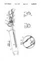
- FIG. 1is an isometric view of a conventional paddle wheel assembly and associated furnace door of the type well known in the field;
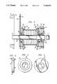
- FIG. 2is a cross-sectional view of the furnace door adjusting apparatus according to the invention.
- FIGS. 3, 4 and 5are respective frontal, rear and side views of the alignment plate utilized according to the invention.
- FIGS. 6 and 7are respective side and frontal Views of the alignment collar utilized in accordance with the invention.
- FIG. 8is a generalized frontal view of the furnace door in different positions occasioned by rotation of the alignment collar.
- FIG. 1the apparatus of the prior art is illustrated in FIG. 1 and described below. Particularly, shown is a wafer paddle assembly 8 commercially available from Cryco-Twenty Two, Inc.
- the illustrated wafer paddle assembly 8operates in conjunction with a furnace assembly including a quartz chamber, manufactured by Thermco, identified as Model 22-600. While not shown, the entire wafer paddle assembly 8 is movable laterally into a quartz chamber 9, under computer control, with respect to a furnace (not shown) for the insertion of semiconductor wafers therein to carry out high temperature processing.
- the wafer paddle assembly 8includes a silicon carbide paddle 10 shaped to accommodate a number of quartz boats for holding semiconductor wafers.
- the paddle 10has an end defined by a square shaft 12 which is held internal to a round paddle holder tube 14.
- a door and sealing assembly 16is fixed around the paddle holder tube 14.
- the paddle holder tube 14is held by a cantilever clamping assembly 18 which, in turn, is adjustably mounted with respect to a base plate 20.
- the base plate 20includes a manual adjustment 22 for providing vertical adjustments of the cantilever clamping assembly 18 and thus adjustments of the wafer paddle 10 within the furnace. While not shown, the base plate 20 is movable laterally by a threaded rod which is rotated by a motor under computer control, thereby laterally moving the entire wafer paddle assembly 8 into and out of the furnace chamber 9. Typically, the lateral travel of the wafer paddle assembly 8 can be about five feet.
- the door sealing assembly 16includes a ten-inch diameter door 24 having an annular O-ring seal 26 fixed to the frontal face thereof.
- the seal 26functions to seal the furnace door 24 to the frontal flange 27 of the furnace chamber.
- Attached to the back side of the furnace door 24is a metal bellows 28 which is longitudinally expandable and contractable with the door 24 with respect to the square portion of the wafer 12 and paddle 10.
- the door 24is longitudinally movable a small amount with respect to the wafer paddle 10 so that the door 24 can be pressed against the flanged opening of the chamber 9 and achieve a seal thereto.
- a collar 29fits between an opening in the door 24 and the square paddle shaft 12.
- the back side of the bellows 28is fastened to an attachment plate 30 by four J-shaped brackets 32.
- a seal 34is held between the attachment plate 30 and the end of the bellows 28. In this manner, the bellows 28 and the attachment plate 30 allow a vacuum to be maintained within the furnace chamber 9.
- the manual adjustment 22can be utilized to adjust the cantilever clamping assembly 18 left and right and thus place the wafer paddle 10 and the semiconductor wafers in the sweet spot of the quartz chamber 9.
- Other adjustmentsare available to move the paddle 10 in small vertical, angular, and other movements.
- the furnace door 24moves accordingly.
- the seal 26may remain flush against the flanged opening 27 of the chamber 9.
- the seal 26does not remain in intimate contact with the furnace opening 27, thereby affecting the processing of the wafers.
- the invention described below in more detailovercomes this problem.
- FIG. 2illustrates a portion of the wafer paddle assembly with some of the parts as supplied with the original equipment, as well as the new parts which allow the entire assembly to function in accordance with the invention.
- the originally-provided parts utilized with the inventioncomprise the paddle 10 and paddle shaft 12, the paddle holder tube 14, the door 24 and associated seal 26, together with the bellows 28, the attachment plate 30, and associated O-ring seal 34 and retainer ring 35 shown in FIG. 2.
- the assembly shown in FIG. 2operates in conjunction with the cantilever clamping assembly 18 and mounting base 20 for providing longitudinal movement of the wafer paddle 10 as well as manual movement in the vertical direction.
- the original collar 29is dispensed with, and a new collar 40 is utilized, as well as an alignment plate 42 and an additional O-ring seal 44 and associated retainer ring 45.
- the bellows 28is sealed to the furnace door 24 by an O-ring 46 and the new collar 40, which also functions as a retainer ring for the O-ring seal 46.
- the accordion-type bellows 28is fixed in a sealed manner at each end thereof with flanges 48 and 50.
- the front flange 48is sealed to the furnace door 24 by the O-ring 46 with the assistance of four J-shaped brackets, one shown as reference numeral 52.
- a bolt 54passes through the bracket 52 and is threaded into the furnace door 24, thereby compressing the O-ring seal 46 between the bellows front flange 48 and the door 24.
- the attachment plate 30is welded to the paddle holder tube 14 by a circular weld 56.
- the alignment plate 42shown in more detail in FIGS. 3, 4 and 5, has thirty-six threaded holes 58 formed in the backside thereof, and four threaded holes 60 formed in the front side thereof.
- the alignment plate 42includes a 1.375 inch radius bore 62 formed in the back face thereof to a depth of 3/16 inch, and a 1.375 inch radius bore 64 formed in the front face thereof offset from the bore 62 by 7/32 inch. Each bore 62 and 64 is formed halfway through the 3/8 inch thick alignment plate 42.
- the threaded holes 58are formed concentrically around the centered bore 62, while the four threaded holes 60 are formed equidistant from the axial axis of the offset bore 64. More particularly, the threaded holes 58 are formed in the back face of the alignment plate 42, spaced apart by ten degrees, at a radius of 2.156 inch from the centered axis about which the central bore 62 is formed. In like manner, the four threaded holes 60 are formed 90 degrees apart and 2.156 inches from the offset axis about which the offset bore 64 is formed. In the preferred embodiment of the invention, the alignment plate 42 is six inches in diameter.
- the centered bore 62receives therein the O-ring seal retainer 35, while the offset bore 64 receives therein and holds the retainer ring 45 around which the O-ring 44 is disposed.
- the alignment collar 40that operates in association with the alignment plate 42 in allowing such parts, as well as the bellows 28 to be rotated when vertical door adjustments are required to maintain the door seal 26 registered with the frontal flange 27 of the wafer processing chamber 9.
- the alignment collar 40has an axial length of about 5/8 inch and an outer diameter of about 3.875 inches.
- a collar bore 70has a diameter of about 2.0625 inches, which is not the same as that of the outside diameter of the paddle holder tube 14, which is about 2.0 inches.
- the collar bore 70is formed about an axis that is offset 19/32 inch from a central axis extending through the collar 40.
- annular O-ring seal 71for cradling a portion of an O-ring seal disposed therearound.
- the surface 73 defined by a circumference of the collar 40rotates freely within a bore formed in the furnace door 24, in which the old collar 29 was previously disposed.
- Both the alignment plate 42 and the alignment collar 40are constructed with 316 stainless steel stock.
- Those skilled in the artmay prefer to utilize a modified alignment collar in conjunction with a standard retainer ring, instead of the single collar 40 shown in FIGS. 6 and 7. If an individual retainer ring is used with a modified collar, then the elements may be spot welded together, and the O-ring 46 slipped over the retaining ring. Further, the collar 40 can be of a longer axial length than shown, if it does not interfere with other apparatus located in the quartz chamber 9.
- the alignment collar 40fits within the opening in the furnace door 24, in such a manner that the alignment collar 40 can be manually rotatable therein. Further, it can be seen that the alignment collar 40 provides internal support to an end of the paddle holder tube 14 which, in turn, provides internal support to the square end 12 of the wafer paddle 10.
- the attachment plate 30has four nonthreaded holes therein through which four bolts 76 pass and are threaded into four of the thirty-six threaded holes 58 formed in the back of the alignment plate 42.
- An elastomeric O-ring 34is positioned between the attachment plate 30 and the alignment plate 42 for providing a seal therebetween.
- the retainer ring 35fits within an annular channel in the attachment rin 30 as well as in the central bore 62 of the alignment plate 42, as described above. While the attachment plate 30 is welded to the paddle holder tube 14, the alignment plate 42 is rotatable about the tube 14 via the opening therethrough that is common to both the central bore 62 and the offset bore 64.
- the partsare not rotatable.
- four J-shaped brackets 32are bolted by corresponding bolts 78 to the four threaded holes 60 formed in the front side of the alignment plate 42.
- the elastomeric O-ring 44is disposed between the alignment plate 42 and the bellows back flange 50 for providing a seal therebetween.
- the O-ring 44is disposed around the retainer ring 45, as noted above, and the ring 45 fits within an annular channel formed in the bellows back flange 50, and in the offset bore 64 formed in the front face of the alignment plate.
- the J-shaped brackets 32bottom out on the alignment plate 42 when the bolts 78 are tightened, thereby preventing excessive compression of the O-ring 44.
- the alignment collar 40, the bellows 28 and the alignment plate 42can be rotatably adjusted in an opposite direction to thereby move the furnace door 24 to a position to maintain its alignment with the flanged end 27 of the quartz chamber 9, while yet maintaining the furnace door 24 in a vertical plane.
- the furnace door 24itself need not be rotated, but does move in a plane when the collar 40 is rotated about the paddle tube 14. On certain occasions, the furnace door 24 itself may need to be rotated to achieve the proper alignment with the quartz chamber flange 27.
- the bellows 28 and its end flanges 48 and 50are also rotated in correspondence with the collar 40 so that the axis of the assembly remains parallel to the axis of the paddle tube 14.
- the alignment plate 42is also rotatably adjusted, which adjustment moves the O-ring 44 and retainer ring 45 on the bellows side thereof, but does not move the O-ring 34 and associated retainer ring 35 on the attachment ring 30 side thereof. This latter action results as the central bore 62 is centered in the alignment plate 42 on the O-ring 34 side, while the offset bore 64 is displaced from the center of the alignment plate 42 on the bellows side.
- the four bolts 54are loosened so that the J-shaped brackets 52 allow the bellows front flange 48 to be rotated with respect to the furnace door 24 which is not rotated.
- the loosened bolts 54also allow the collar 40 to be rotated.
- the four bolts 76 passing through the attachment plate 30are completely removed from their threaded engagement in the alignment plate 42.
- the bolts 78remain tightened in the front side of the alignment plate 42.
- the alignment plate 42 and attached bellows 28are rotated as a unit an angular amount sufficient to provide appropriate vertical adjustment for the furnace door 24.
- the alignment collar 40is loosened by loosening bolts 54 as noted above, and the collar is also rotated in the same direction and amount as the alignment plate 42.
- the adjustment of the alignment collar 40brings the furnace door 24 back into a vertical plane so that a suitable seal can be maintained between the O-ring 26 and the frontal flange 27 of the quartz chamber 9.
- the four bolts 76are then threaded into four of the corresponding thirty-six threaded holes 58 and tightened.
- the bolts 54are tightened so that the J-shaped brackets 52 secure and seal the alignment collar 40 between the bellows front flange 48 and the rear surface of the furnace door 24. If finer rotational adjustments of the alignment plate 42 and the bellows 28 are required, then additional threaded holes 58 can be formed in the back face of the alignment plate 42 as shown in FIG. 4.
- both the alignment plate 42 and the alignment collar 40have offset bores formed therethrough, the rotational movement of both such members causes the apparatus associated therewith to be also moved along an axis that is parallel to, but offset from that of the paddle tube 14.
- the furnace door 24is required to move in a vertical plane to maintain registration with the vertical flanged surface 27 of the quartz chamber.
- FIG. 8The furnace door 24 is shown in solid line in a position when the offset bore 70 of the alignment collar 40 is rotated in its uppermost vertical position, while the broken line depicts the furnace door 24 lowered a maximum amount by the rotation of the collar 40 so that the offset bore 70 is in its lowermost vertical position.
- the opening in the door 24 through which a portion of the collar 40 is disposeddoes not move as a result of collar rotation.
- the door 24does move when the entire paddle assembly 8 is moved by movement of the cantilever clamping assembly 18.
- intermediate positions of the furnace door 24can be achieved by rotation of the collar 40 to positions intermediate that shown in FIG. 8, although the furnace door will encounter slight horizontal displacements at such positions. This sideways displacement of the door 24 is compensated by counter rotation of the door to bring the sealing ring 26 centered with respect to the furnace flange 27.
- the inventionprovides a technique for adjusting CVD furnaces without affecting the placement of the process loads as located on the paddle. While the preferred embodiment of the invention has been disclosed with reference to specific furnace door alignment apparatus, it is to be understood that many changes in detail may be made as a matter of engineering choices, without departing from the spirit and scope of the invention, as defined by the appended claims.
Landscapes
- Chemical & Material Sciences (AREA)
- Engineering & Computer Science (AREA)
- Crystallography & Structural Chemistry (AREA)
- Materials Engineering (AREA)
- Metallurgy (AREA)
- Organic Chemistry (AREA)
Abstract
Description
The present invention relates in general to semiconductor processing furnaces, and more particularly to apparatus and techniques for aligning a diffusion furnace door to allow adjustment of the paddle assembly while yet maintaining the furnace door aligned and sealed to the furnace unit.
The fabrication of semiconductor circuits involves many process steps for forming active and passive components in a semiconductor substrate. Many of the processing steps are carried out at high temperatures for depositing dopants or materials in or on the surface of the semiconductor wafer. Furnaces especially adapted for processing semiconductor wafers in a controlled environment are commercially available. Wafer processing furnaces generally include a quartz cylinder in which the wafers are disposed in an evacuated chamber. Temperatures generated by the furnace and conducted to the quartz chamber are typically in the range of 400° C. to 700° C., depending upon the particular process and materials involved. Further, the quartz tube has an inlet and outlet through which various gases can be passed to subject the semiconductor wafers to the desired temperature, as well as various chemical compositions according to a recipe. It is well known that optimum performance and yield of the wafers are dependent upon the uniformity of temperature and gas distribution within the quartz chamber.
While many different types of wafer processing furnaces are available, many such furnaces utilize a quartz chamber having a frontal flanged opening. A wafer paddle assembly, including the furnace door, is externally movable, generally under computer control, for moving the paddle assembly into the horizontally situated quartz chamber. The paddle assembly holds a number of wafers at the end thereof, and has affixed thereto the furnace door that seals to the opening when the paddle assembly is fully inserted into the quartz chamber. The chamber is pumped down to a desired vacuum, the furnace is heated to a desired temperature, and then the appropriate gases are passed through the quartz chamber for depositing various material layers on or in the wafers. Such a process is commonly known as chemical vapor deposition (CVD). Many other processes can be carried out with such furnaces. As noted above, optimum processing occurs in the quartz chamber at a certain location, termed a "sweet spot", where the temperature and chemical composition are maintained at desired parameters prescribed in the processing recipe. By trial and error techniques, or by conducting tests on test wafers, the exact sweet spot location and size of each furnace can be found. In order to precisely place the semiconductor wafers in the sweet spot, the paddle assembly often requires vertical or horizontal adjustments. The paddle assembly itself can generally accommodate small adjustments in a vertical or lateral direction without substantially affecting the seal of the door to the quartz chamber. However, situations often arises in which the paddle assembly cannot be adequately ad3usted in the sweet spot without affecting the seal between the furnace door and the quartz chamber. In this situation, wafer processing must be carried out at a location in the chamber that is suboptimal, thereby compromising the yield of the die on each wafer. As a result, the cost per circuit die increases, and sometimes entire batches of wafers are destroyed or unusable due to an inadequate vacuum seal between the furnace door and processing chamber.
From the foregoing, it can be seen that a need exists for an apparatus and technique for allowing adjustability between the paddle assembly and the furnace door so that a wider degree of adjustability is afforded, without affecting the seal between the furnace door and the temperature chamber. Another need exists for a technique providing the noted adjustability that is simplified and does not require precision equipment, apparatus or a high degree of operator expertise.
In accordance with the invention, there are disclosed herein techniques and apparatus for providing adjustments of a furnace door with respect to a wafer paddle assembly, thereby avoiding or substantially eliminating the shortcomings of the prior art apparatus and techniques. In accordance with an important aspect of the invention, a furnace door is made adjustable in an eccentric manner with respect to the paddle assembly so that both lateral and vertical adjustments therebetween are available.
According to a preferred embodiment of the invention, a furnace door and associated coupling bellows are mounted around a paddle shaft assembly by a tubular frontal collar and a circular rear spacer plate. Importantly, the frontal collar has a bore formed therethrough offset from a central axis thereof. The spacer plate has a central bore formed halfway therethrough in one face, and an offset bore formed halfway therethrough in the opposite face. A resulting or oblong opening is thus formed through the spacer plate, through which the paddle assembly tube extends. The offset bore in the alignment plate holds a retainer ring around which an 0-ring is placed to seal one end of the bellows to the alignment plate. A similar seal arrangement provides a seal between the other end of the bellows and the furnace door itself. The frontal collar fits within a circular opening in the furnace door, while the spacer ring is rotatably attached and sealed to a back plate that is fixed to the paddle tube. With this arrangement, when it is desired to adjust the paddle tube in a direction that would otherwise result in an inadequate seal between the furnace door and the chamber, the entire spacer plate, bellows, door and collar can be moved to bring the door back into alignment with the frontal surface of the quartz chamber, thereby assuring a suitable seal therebetween and the placement of the wafer paddle in the sweet spot of the furnace.
Further features and advantages will become apparent from the following and more particular description of the preferred embodiment of the invention, as illustrated in the accompanying drawings in which like reference characters generally refer to the same parts, elements or functions throughout the views, and in which:
FIG. 1 is an isometric view of a conventional paddle wheel assembly and associated furnace door of the type well known in the field;
FIG. 2 is a cross-sectional view of the furnace door adjusting apparatus according to the invention;
FIGS. 3, 4 and 5 are respective frontal, rear and side views of the alignment plate utilized according to the invention;
FIGS. 6 and 7 are respective side and frontal Views of the alignment collar utilized in accordance with the invention; and
FIG. 8 is a generalized frontal view of the furnace door in different positions occasioned by rotation of the alignment collar.
In order to facilitate understanding and appreciation of the present invention, the apparatus of the prior art is illustrated in FIG. 1 and described below. Particularly, shown is awafer paddle assembly 8 commercially available from Cryco-Twenty Two, Inc. The illustratedwafer paddle assembly 8 operates in conjunction with a furnace assembly including a quartz chamber, manufactured by Thermco, identified as Model 22-600. While not shown, the entirewafer paddle assembly 8 is movable laterally into aquartz chamber 9, under computer control, with respect to a furnace (not shown) for the insertion of semiconductor wafers therein to carry out high temperature processing. Thewafer paddle assembly 8 includes asilicon carbide paddle 10 shaped to accommodate a number of quartz boats for holding semiconductor wafers. Thepaddle 10 has an end defined by asquare shaft 12 which is held internal to a roundpaddle holder tube 14. A door andsealing assembly 16 is fixed around thepaddle holder tube 14. Thepaddle holder tube 14 is held by acantilever clamping assembly 18 which, in turn, is adjustably mounted with respect to abase plate 20. Thebase plate 20 includes amanual adjustment 22 for providing vertical adjustments of thecantilever clamping assembly 18 and thus adjustments of thewafer paddle 10 within the furnace. While not shown, thebase plate 20 is movable laterally by a threaded rod which is rotated by a motor under computer control, thereby laterally moving the entirewafer paddle assembly 8 into and out of thefurnace chamber 9. Typically, the lateral travel of thewafer paddle assembly 8 can be about five feet.
Thedoor sealing assembly 16 includes a ten-inch diameter door 24 having an annular O-ring seal 26 fixed to the frontal face thereof. Theseal 26 functions to seal thefurnace door 24 to thefrontal flange 27 of the furnace chamber. Attached to the back side of thefurnace door 24 is ametal bellows 28 which is longitudinally expandable and contractable with thedoor 24 with respect to the square portion of thewafer 12 andpaddle 10. Thedoor 24 is longitudinally movable a small amount with respect to thewafer paddle 10 so that thedoor 24 can be pressed against the flanged opening of thechamber 9 and achieve a seal thereto. In particular, acollar 29 fits between an opening in thedoor 24 and thesquare paddle shaft 12. The back side of thebellows 28 is fastened to anattachment plate 30 by four J-shaped brackets 32. Aseal 34 is held between theattachment plate 30 and the end of thebellows 28. In this manner, thebellows 28 and theattachment plate 30 allow a vacuum to be maintained within thefurnace chamber 9.
As noted above, themanual adjustment 22 can be utilized to adjust thecantilever clamping assembly 18 left and right and thus place thewafer paddle 10 and the semiconductor wafers in the sweet spot of thequartz chamber 9. Other adjustments (not shown) are available to move thepaddle 10 in small vertical, angular, and other movements. As can be appreciated, as thewafer paddle 10 is adjusted up or down, thefurnace door 24 moves accordingly. Depending upon the amount of movement, which may be 1/16 inch-1.5 inches, theseal 26 may remain flush against theflanged opening 27 of thechamber 9. However, there may be instances in which theseal 26 does not remain in intimate contact with thefurnace opening 27, thereby affecting the processing of the wafers. The invention described below in more detail, overcomes this problem.
FIG. 2 illustrates a portion of the wafer paddle assembly with some of the parts as supplied with the original equipment, as well as the new parts which allow the entire assembly to function in accordance with the invention. The originally-provided parts utilized with the invention comprise thepaddle 10 andpaddle shaft 12, thepaddle holder tube 14, thedoor 24 and associatedseal 26, together with thebellows 28, theattachment plate 30, and associated O-ring seal 34 andretainer ring 35 shown in FIG. 2. Of course, the assembly shown in FIG. 2 operates in conjunction with thecantilever clamping assembly 18 and mountingbase 20 for providing longitudinal movement of thewafer paddle 10 as well as manual movement in the vertical direction. In accordance with the preferred form of the invention, theoriginal collar 29 is dispensed with, and anew collar 40 is utilized, as well as analignment plate 42 and an additional O-ring seal 44 and associatedretainer ring 45. The bellows 28 is sealed to thefurnace door 24 by an O-ring 46 and thenew collar 40, which also functions as a retainer ring for the O-ring seal 46. The accordion-type bellows 28 is fixed in a sealed manner at each end thereof withflanges front flange 48 is sealed to thefurnace door 24 by the O-ring 46 with the assistance of four J-shaped brackets, one shown asreference numeral 52. Abolt 54 passes through thebracket 52 and is threaded into thefurnace door 24, thereby compressing the O-ring seal 46 between the bellowsfront flange 48 and thedoor 24.
As further noted in FIG. 2, theattachment plate 30 is welded to thepaddle holder tube 14 by acircular weld 56. Thealignment plate 42, shown in more detail in FIGS. 3, 4 and 5, has thirty-six threadedholes 58 formed in the backside thereof, and four threadedholes 60 formed in the front side thereof. Importantly, thealignment plate 42 includes a 1.375 inch radius bore 62 formed in the back face thereof to a depth of 3/16 inch, and a 1.375 inch radius bore 64 formed in the front face thereof offset from thebore 62 by 7/32 inch. Each bore 62 and 64 is formed halfway through the 3/8 inchthick alignment plate 42. The threaded holes 58 are formed concentrically around the centered bore 62, while the four threadedholes 60 are formed equidistant from the axial axis of the offset bore 64. More particularly, the threadedholes 58 are formed in the back face of thealignment plate 42, spaced apart by ten degrees, at a radius of 2.156 inch from the centered axis about which thecentral bore 62 is formed. In like manner, the four threadedholes 60 are formed 90 degrees apart and 2.156 inches from the offset axis about which the offset bore 64 is formed. In the preferred embodiment of the invention, thealignment plate 42 is six inches in diameter. The centered bore 62 receives therein the O-ring seal retainer 35, while the offset bore 64 receives therein and holds theretainer ring 45 around which the O-ring 44 is disposed.
With reference now to FIGS. 6 and 7, there is illustrated thealignment collar 40 that operates in association with thealignment plate 42 in allowing such parts, as well as thebellows 28 to be rotated when vertical door adjustments are required to maintain thedoor seal 26 registered with thefrontal flange 27 of thewafer processing chamber 9. In the preferred embodiment the invention, thealignment collar 40 has an axial length of about 5/8 inch and an outer diameter of about 3.875 inches. A collar bore 70 has a diameter of about 2.0625 inches, which is not the same as that of the outside diameter of thepaddle holder tube 14, which is about 2.0 inches. The collar bore 70 is formed about an axis that is offset 19/32 inch from a central axis extending through thecollar 40. Formed integral with thecollar 40 is an annular O-ring seal 71 for cradling a portion of an O-ring seal disposed therearound. Thesurface 73 defined by a circumference of thecollar 40 rotates freely within a bore formed in thefurnace door 24, in which theold collar 29 was previously disposed. Both thealignment plate 42 and thealignment collar 40 are constructed with 316 stainless steel stock. Those skilled in the art may prefer to utilize a modified alignment collar in conjunction with a standard retainer ring, instead of thesingle collar 40 shown in FIGS. 6 and 7. If an individual retainer ring is used with a modified collar, then the elements may be spot welded together, and the O-ring 46 slipped over the retaining ring. Further, thecollar 40 can be of a longer axial length than shown, if it does not interfere with other apparatus located in thequartz chamber 9.
With regard again to FIG. 2, it should be noted that thealignment collar 40 fits within the opening in thefurnace door 24, in such a manner that thealignment collar 40 can be manually rotatable therein. Further, it can be seen that thealignment collar 40 provides internal support to an end of thepaddle holder tube 14 which, in turn, provides internal support to thesquare end 12 of thewafer paddle 10.
As further noted in FIG. 2, theattachment plate 30 has four nonthreaded holes therein through which fourbolts 76 pass and are threaded into four of the thirty-six threadedholes 58 formed in the back of thealignment plate 42. An elastomeric O-ring 34 is positioned between theattachment plate 30 and thealignment plate 42 for providing a seal therebetween. Theretainer ring 35 fits within an annular channel in the attachment rin 30 as well as in thecentral bore 62 of thealignment plate 42, as described above. While theattachment plate 30 is welded to thepaddle holder tube 14, thealignment plate 42 is rotatable about thetube 14 via the opening therethrough that is common to both thecentral bore 62 and the offset bore 64. Of course, when fastened by thebolts 76 to theattachment plate 30, the parts are not rotatable. As noted above, four J-shapedbrackets 32 are bolted by correspondingbolts 78 to the four threadedholes 60 formed in the front side of thealignment plate 42. The elastomeric O-ring 44 is disposed between thealignment plate 42 and the bellows backflange 50 for providing a seal therebetween. The O-ring 44 is disposed around theretainer ring 45, as noted above, and thering 45 fits within an annular channel formed in the bellows backflange 50, and in the offset bore 64 formed in the front face of the alignment plate. The J-shapedbrackets 32 bottom out on thealignment plate 42 when thebolts 78 are tightened, thereby preventing excessive compression of the O-ring 44.
Were it not for the invention depicted in connection with FIG. 2, in an attempt to rotate thedoor 24 with the apparatus shown in FIG. 1 to achieve alignment with the flanged end of the quartz chamber, thedoor 24 would be tilted from a vertical plane and thereby exacerbate attempts to achieve a suitable seal to theflanged end 27 of thequartz chamber 9. However, by utilizing the principles and concepts of the invention, movements of thewafer paddle 10 occasioned by the manual cantilever clamping assembly adjustments which otherwise would result in misalignment of thefurnace door 24, can be compensated or offset by corresponding rotational adjustments of thealignment plate 42, thebellows 28, thealignment collar 40 and even thedoor 24 itself. In other words, when thewafer paddle 10 is ideally adjusted in one direction within the quartz chamber in the sweet spot thereof, thealignment collar 40, thebellows 28 and thealignment plate 42 can be rotatably adjusted in an opposite direction to thereby move thefurnace door 24 to a position to maintain its alignment with theflanged end 27 of thequartz chamber 9, while yet maintaining thefurnace door 24 in a vertical plane. It should be noted that thefurnace door 24 itself need not be rotated, but does move in a plane when thecollar 40 is rotated about thepaddle tube 14. On certain occasions, thefurnace door 24 itself may need to be rotated to achieve the proper alignment with thequartz chamber flange 27. The bellows 28 and itsend flanges collar 40 so that the axis of the assembly remains parallel to the axis of thepaddle tube 14. Thealignment plate 42 is also rotatably adjusted, which adjustment moves the O-ring 44 andretainer ring 45 on the bellows side thereof, but does not move the O-ring 34 and associatedretainer ring 35 on theattachment ring 30 side thereof. This latter action results as thecentral bore 62 is centered in thealignment plate 42 on the O-ring 34 side, while the offset bore 64 is displaced from the center of thealignment plate 42 on the bellows side. Were it not for the tendency of the furnace door to tilt when only thecollar 40 is rotated, theback flange 50 andalignment plate 42 would not need to be provided with offset apparatus. In other words, if thebellows 28 were of the type that could be bent so as to exhibit a circuitous axial axis, only thecollar 40 would be adjusted to displace thefurnace door 24 without also having to rotate thealignment plate 42 and thebellows 28.
The manner in which the foregoing adjustments are accomplished is described in the following manner. First, the fourbolts 54 are loosened so that the J-shapedbrackets 52 allow the bellowsfront flange 48 to be rotated with respect to thefurnace door 24 which is not rotated. The loosenedbolts 54 also allow thecollar 40 to be rotated. The fourbolts 76 passing through theattachment plate 30 are completely removed from their threaded engagement in thealignment plate 42. Thebolts 78 remain tightened in the front side of thealignment plate 42. Then, thealignment plate 42 and attached bellows 28 are rotated as a unit an angular amount sufficient to provide appropriate vertical adjustment for thefurnace door 24. In like manner, thealignment collar 40 is loosened by looseningbolts 54 as noted above, and the collar is also rotated in the same direction and amount as thealignment plate 42. The adjustment of thealignment collar 40 brings thefurnace door 24 back into a vertical plane so that a suitable seal can be maintained between the O-ring 26 and thefrontal flange 27 of thequartz chamber 9. The fourbolts 76 are then threaded into four of the corresponding thirty-six threadedholes 58 and tightened. Then, thebolts 54 are tightened so that the J-shapedbrackets 52 secure and seal thealignment collar 40 between the bellowsfront flange 48 and the rear surface of thefurnace door 24. If finer rotational adjustments of thealignment plate 42 and thebellows 28 are required, then additional threadedholes 58 can be formed in the back face of thealignment plate 42 as shown in FIG. 4.
As can be appreciated from the foregoing, because both thealignment plate 42 and thealignment collar 40 have offset bores formed therethrough, the rotational movement of both such members causes the apparatus associated therewith to be also moved along an axis that is parallel to, but offset from that of thepaddle tube 14. As noted above, whether or not thefurnace door 24 is itself rotated, it is required to move in a vertical plane to maintain registration with the verticalflanged surface 27 of the quartz chamber. This aspect is shown in FIG. 8. Thefurnace door 24 is shown in solid line in a position when the offset bore 70 of thealignment collar 40 is rotated in its uppermost vertical position, while the broken line depicts thefurnace door 24 lowered a maximum amount by the rotation of thecollar 40 so that the offset bore 70 is in its lowermost vertical position. As noted, the opening in thedoor 24 through which a portion of thecollar 40 is disposed does not move as a result of collar rotation. Thedoor 24 does move when theentire paddle assembly 8 is moved by movement of thecantilever clamping assembly 18. Of course, intermediate positions of thefurnace door 24 can be achieved by rotation of thecollar 40 to positions intermediate that shown in FIG. 8, although the furnace door will encounter slight horizontal displacements at such positions. This sideways displacement of thedoor 24 is compensated by counter rotation of the door to bring the sealingring 26 centered with respect to thefurnace flange 27.
From the foregoing, the invention provides a technique for adjusting CVD furnaces without affecting the placement of the process loads as located on the paddle. While the preferred embodiment of the invention has been disclosed with reference to specific furnace door alignment apparatus, it is to be understood that many changes in detail may be made as a matter of engineering choices, without departing from the spirit and scope of the invention, as defined by the appended claims.
Claims (22)
1. Furnace door alignment apparatus, comprising:
a furnace door movable with respect to an opening in said furnace, said door having an opening through which paddle apparatus is disposed so that said paddle apparatus is located in the furnace while said door is sealed to the furnace opening; and
an alignment collar supporting said paddle apparatus with respect to said furnace door, said alignment collar having a bore therein through which said paddle apparatus passes, and said bore being offset from a central axis of said alignment collar so that when said alignment collar is rotated about said paddle apparatus, said door is moved with respect to said central axis.
2. The furnace door alignment apparatus of claim 1, wherein said alignment collar has an annular area therearound for accommodating an O-ring type of seal.
3. The furnace door alignment apparatus of claim 1, further including an alignment plate having a central axis, and a bore in said alignment plate being offset with respect to the central axis of the alignment plate, said alignment plate bore being sized for passing the paddle apparatus therethrough.
4. The furnace door alignment apparatus of claim 3, wherein said alignment plate includes a central bore and an offset bore, each bore formed halfway through the alignment plate in opposing faces thereof, and said paddle apparatus passes through a bore portion that is common to said central and offset bores.
5. The furnace door alignment apparatus of claim 4, further including a bellows attachable to said alignment plate, and a seal engageable with said offset bore in said alignment plate.
6. The furnace door alignment apparatus of claim 3, further including a bellows attachable to said alignment plate at one end of the bellows and attachable to said furnace door at an opposite end thereof.
7. The furnace door alignment apparatus of claim 6, wherein said bellows includes a front flange and a back flange, and further including a pair of O-ring seals for sealing respectively to said front and back bellows flanges.
8. The furnace door alignment apparatus of claim 6, further including an attachment plate fixed to said paddle apparatus, and means for fastening the alignment plate to said attachment plate.
9. The furnace door alignment apparatus of claim 8, wherein said alignment plate includes threaded holes in a back face thereof for attachment by bolts to said attachment plate, said bellows having a front and back flange, and a plurality of threaded holes in a front face of said alignment plate for attachment to said bellows back flange.
10. The furnace door alignment apparatus of claim 9, wherein said alignment plate is fastened to said bellows back flange by a plurality of bolts and associated J-shaped brackets.
11. Furnace door alignment apparatus for use with a water processing furnace, comprising:
a furnace door movable with respect to an opening in said furnace, said door having an openign through which padde apparatus is disposed so that said paddle apparatus is disposed in the furnace while said door is sealed to the furnace opening;
an attachment plate fixed with respect to said paddle apparatus;
an alignment plate having a central axis, and a bore in said alignment plate offset with respect to said central plate axis, said alignment plate bore being sized for passing the paddle apparatus therethrough;
an alignment collar having a central axis, and a bore in said alignment collar being offset with respect to said alignment collar central axis, said alignment collar bore supporting the paddle apparatus and fitting within the opening in said furnace door;
a bellows having a front end sealed to said furnace door, and a back end with a seal arrangement engageable with the offset bore in said alignment plate;
means for selaing the furnace door to said wafer processing furnace; and
said alignment plate and said alignment collar being movable at desired angular positions with respect to said paddle apparatus.
12. The furnace door alignment apparatus of claim 11, wherein said bellows seal arrangement includes a retainer ring disposed in the offset bore of said alignment plate, and an O-ring disposed around said retainer ring.
13. The furnace door alignment apparatus of claim 11, further including a plurality of threaded holes in one side face of said alignment plate, and means for fixing said attachment plate to said alignment plate using said threaded holes.
14. The furnace door alignment apparatus of claim 13, wherein said alignment plate includes a central bore formed in oen face thereof and halfway therethrough, and said offset bore is formed halfway through said alignment plate on an opposite face thereof, thereby forming a bore portion common to said central and offset bores, said paddle assembly passing through said common bore portion.
15. The furnace door alignment apparatus of claim 13, wherein said alignment plate includes a plurality of threaded holes in an opposite face for fastening thereto said bellows.
16. The furnace door alignment apparatus of claim 11, wherein said alignment collar includes an annular groove therearound for accommodating an O-ring therein.
17. A method for adjusting a furnace door with respec to a furnace opening in wafer processing furnace equipment of the type having a furnace and a door held against an opening in the furnace, and wafer paddle apparatus disposed through the door and attachable thereto, and a bellows and seals for sealing the furnace door to the paddle apparatus, the method comprising the steps of:
mounting an alignment plate for angular movements about said paddle apparatus;
mounting an alignment collar for angular movements about said paddle apparatus;
mounting the bellows to said alignment plate so that angular movements of said alignment plate displace a central axis of said bellows from a central axis of said paddle apparatus;
mounting the alignment collar to the furnace door so the angular movements thereof cause a central axis of the door to be displaced from the central axis of said paddle apparatus; and
mounting the bellows to the furnace door.
18. The method of claim 17, further including forming an offset bore in said alignment plate and an offset bore in said alignment collar, and passing both said offset bores said paddle apparatus.
19. The method of claim 18, further including engaging a seal ring to said offset bore in said alignment plate so that a seal engaged with said seal ring moves with said bellows.
20. The method of claim 17, further including attaching said alignment plate to an attachment plate that is fixed to said paddle apapratus.
21. The method of claim 20, further including sealing said attachment plate to said alignment plate with an O-ring seal and a retainer ring so that said O-ring does not move with respect to the paddle apparatus axis when said alignment plate is rotated.
22. The method of claim 17, further including rotating said alignment collar about its offset axis, thereby moving said furnace door in a vertical plane without tilting the furnace door.
Priority Applications (1)
| Application Number | Priority Date | Filing Date | Title |
|---|---|---|---|
| US07/843,537US5208961A (en) | 1992-02-28 | 1992-02-28 | Semiconductor processing furnace door alignment apparatus and method |
Applications Claiming Priority (1)
| Application Number | Priority Date | Filing Date | Title |
|---|---|---|---|
| US07/843,537US5208961A (en) | 1992-02-28 | 1992-02-28 | Semiconductor processing furnace door alignment apparatus and method |
Publications (1)
| Publication Number | Publication Date |
|---|---|
| US5208961Atrue US5208961A (en) | 1993-05-11 |
Family
ID=25290302
Family Applications (1)
| Application Number | Title | Priority Date | Filing Date |
|---|---|---|---|
| US07/843,537Expired - LifetimeUS5208961A (en) | 1992-02-28 | 1992-02-28 | Semiconductor processing furnace door alignment apparatus and method |
Country Status (1)
| Country | Link |
|---|---|
| US (1) | US5208961A (en) |
Cited By (259)
| Publication number | Priority date | Publication date | Assignee | Title |
|---|---|---|---|---|
| US6631934B1 (en)* | 2000-06-02 | 2003-10-14 | Saint-Gobain Ceramics & Plastics, Inc. | Silicon carbide cantilever paddle |
| US20050090923A1 (en)* | 2003-09-03 | 2005-04-28 | Norman Rieker | Method for monitoring a batch system |
| US20110147140A1 (en)* | 2005-07-06 | 2011-06-23 | Wabtec Holding Corp. | Universal brake assembly |
| USD714369S1 (en) | 2011-11-23 | 2014-09-30 | Coorstek, Inc. | Wafer paddle |
| USD842951S1 (en)* | 2017-11-10 | 2019-03-12 | Ogosport Llc | Paddle |
| US11164955B2 (en) | 2017-07-18 | 2021-11-02 | Asm Ip Holding B.V. | Methods for forming a semiconductor device structure and related semiconductor device structures |
| US11171025B2 (en) | 2019-01-22 | 2021-11-09 | Asm Ip Holding B.V. | Substrate processing device |
| US11168395B2 (en) | 2018-06-29 | 2021-11-09 | Asm Ip Holding B.V. | Temperature-controlled flange and reactor system including same |
| US11205585B2 (en)* | 2016-07-28 | 2021-12-21 | Asm Ip Holding B.V. | Substrate processing apparatus and method of operating the same |
| US11217444B2 (en) | 2018-11-30 | 2022-01-04 | Asm Ip Holding B.V. | Method for forming an ultraviolet radiation responsive metal oxide-containing film |
| US11222772B2 (en) | 2016-12-14 | 2022-01-11 | Asm Ip Holding B.V. | Substrate processing apparatus |
| USD940837S1 (en) | 2019-08-22 | 2022-01-11 | Asm Ip Holding B.V. | Electrode |
| US11227789B2 (en) | 2019-02-20 | 2022-01-18 | Asm Ip Holding B.V. | Method and apparatus for filling a recess formed within a substrate surface |
| US11227782B2 (en) | 2019-07-31 | 2022-01-18 | Asm Ip Holding B.V. | Vertical batch furnace assembly |
| US11233133B2 (en) | 2015-10-21 | 2022-01-25 | Asm Ip Holding B.V. | NbMC layers |
| US11230766B2 (en) | 2018-03-29 | 2022-01-25 | Asm Ip Holding B.V. | Substrate processing apparatus and method |
| US11232963B2 (en) | 2018-10-03 | 2022-01-25 | Asm Ip Holding B.V. | Substrate processing apparatus and method |
| US11242598B2 (en) | 2015-06-26 | 2022-02-08 | Asm Ip Holding B.V. | Structures including metal carbide material, devices including the structures, and methods of forming same |
| US11251035B2 (en) | 2016-12-22 | 2022-02-15 | Asm Ip Holding B.V. | Method of forming a structure on a substrate |
| US11251068B2 (en) | 2018-10-19 | 2022-02-15 | Asm Ip Holding B.V. | Substrate processing apparatus and substrate processing method |
| US11251040B2 (en) | 2019-02-20 | 2022-02-15 | Asm Ip Holding B.V. | Cyclical deposition method including treatment step and apparatus for same |
| USD944946S1 (en) | 2019-06-14 | 2022-03-01 | Asm Ip Holding B.V. | Shower plate |
| US11270899B2 (en) | 2018-06-04 | 2022-03-08 | Asm Ip Holding B.V. | Wafer handling chamber with moisture reduction |
| US11274369B2 (en) | 2018-09-11 | 2022-03-15 | Asm Ip Holding B.V. | Thin film deposition method |
| US11282698B2 (en) | 2019-07-19 | 2022-03-22 | Asm Ip Holding B.V. | Method of forming topology-controlled amorphous carbon polymer film |
| US11286562B2 (en) | 2018-06-08 | 2022-03-29 | Asm Ip Holding B.V. | Gas-phase chemical reactor and method of using same |
| US11286558B2 (en) | 2019-08-23 | 2022-03-29 | Asm Ip Holding B.V. | Methods for depositing a molybdenum nitride film on a surface of a substrate by a cyclical deposition process and related semiconductor device structures including a molybdenum nitride film |
| US11289326B2 (en) | 2019-05-07 | 2022-03-29 | Asm Ip Holding B.V. | Method for reforming amorphous carbon polymer film |
| US11295980B2 (en) | 2017-08-30 | 2022-04-05 | Asm Ip Holding B.V. | Methods for depositing a molybdenum metal film over a dielectric surface of a substrate by a cyclical deposition process and related semiconductor device structures |
| USD947913S1 (en) | 2019-05-17 | 2022-04-05 | Asm Ip Holding B.V. | Susceptor shaft |
| US11296189B2 (en) | 2018-06-21 | 2022-04-05 | Asm Ip Holding B.V. | Method for depositing a phosphorus doped silicon arsenide film and related semiconductor device structures |
| USD949319S1 (en) | 2019-08-22 | 2022-04-19 | Asm Ip Holding B.V. | Exhaust duct |
| US11306395B2 (en) | 2017-06-28 | 2022-04-19 | Asm Ip Holding B.V. | Methods for depositing a transition metal nitride film on a substrate by atomic layer deposition and related deposition apparatus |
| US11315794B2 (en) | 2019-10-21 | 2022-04-26 | Asm Ip Holding B.V. | Apparatus and methods for selectively etching films |
| US11339476B2 (en) | 2019-10-08 | 2022-05-24 | Asm Ip Holding B.V. | Substrate processing device having connection plates, substrate processing method |
| US11342216B2 (en) | 2019-02-20 | 2022-05-24 | Asm Ip Holding B.V. | Cyclical deposition method and apparatus for filling a recess formed within a substrate surface |
| US11345999B2 (en) | 2019-06-06 | 2022-05-31 | Asm Ip Holding B.V. | Method of using a gas-phase reactor system including analyzing exhausted gas |
| US11355338B2 (en) | 2019-05-10 | 2022-06-07 | Asm Ip Holding B.V. | Method of depositing material onto a surface and structure formed according to the method |
| US11361990B2 (en) | 2018-05-28 | 2022-06-14 | Asm Ip Holding B.V. | Substrate processing method and device manufactured by using the same |
| US11374112B2 (en) | 2017-07-19 | 2022-06-28 | Asm Ip Holding B.V. | Method for depositing a group IV semiconductor and related semiconductor device structures |
| US11378337B2 (en) | 2019-03-28 | 2022-07-05 | Asm Ip Holding B.V. | Door opener and substrate processing apparatus provided therewith |
| US11387120B2 (en) | 2017-09-28 | 2022-07-12 | Asm Ip Holding B.V. | Chemical dispensing apparatus and methods for dispensing a chemical to a reaction chamber |
| US11387106B2 (en) | 2018-02-14 | 2022-07-12 | Asm Ip Holding B.V. | Method for depositing a ruthenium-containing film on a substrate by a cyclical deposition process |
| US11390950B2 (en) | 2017-01-10 | 2022-07-19 | Asm Ip Holding B.V. | Reactor system and method to reduce residue buildup during a film deposition process |
| US11390946B2 (en) | 2019-01-17 | 2022-07-19 | Asm Ip Holding B.V. | Methods of forming a transition metal containing film on a substrate by a cyclical deposition process |
| US11393690B2 (en) | 2018-01-19 | 2022-07-19 | Asm Ip Holding B.V. | Deposition method |
| US11390945B2 (en) | 2019-07-03 | 2022-07-19 | Asm Ip Holding B.V. | Temperature control assembly for substrate processing apparatus and method of using same |
| US11398382B2 (en) | 2018-03-27 | 2022-07-26 | Asm Ip Holding B.V. | Method of forming an electrode on a substrate and a semiconductor device structure including an electrode |
| US11396702B2 (en) | 2016-11-15 | 2022-07-26 | Asm Ip Holding B.V. | Gas supply unit and substrate processing apparatus including the gas supply unit |
| US11401605B2 (en) | 2019-11-26 | 2022-08-02 | Asm Ip Holding B.V. | Substrate processing apparatus |
| US11411088B2 (en) | 2018-11-16 | 2022-08-09 | Asm Ip Holding B.V. | Methods for forming a metal silicate film on a substrate in a reaction chamber and related semiconductor device structures |
| US11410851B2 (en) | 2017-02-15 | 2022-08-09 | Asm Ip Holding B.V. | Methods for forming a metallic film on a substrate by cyclical deposition and related semiconductor device structures |
| US11417545B2 (en) | 2017-08-08 | 2022-08-16 | Asm Ip Holding B.V. | Radiation shield |
| US11414760B2 (en) | 2018-10-08 | 2022-08-16 | Asm Ip Holding B.V. | Substrate support unit, thin film deposition apparatus including the same, and substrate processing apparatus including the same |
| US11424119B2 (en) | 2019-03-08 | 2022-08-23 | Asm Ip Holding B.V. | Method for selective deposition of silicon nitride layer and structure including selectively-deposited silicon nitride layer |
| US11430640B2 (en) | 2019-07-30 | 2022-08-30 | Asm Ip Holding B.V. | Substrate processing apparatus |
| US11430674B2 (en) | 2018-08-22 | 2022-08-30 | Asm Ip Holding B.V. | Sensor array, apparatus for dispensing a vapor phase reactant to a reaction chamber and related methods |
| US11437241B2 (en) | 2020-04-08 | 2022-09-06 | Asm Ip Holding B.V. | Apparatus and methods for selectively etching silicon oxide films |
| US11443926B2 (en) | 2019-07-30 | 2022-09-13 | Asm Ip Holding B.V. | Substrate processing apparatus |
| US11447864B2 (en) | 2019-04-19 | 2022-09-20 | Asm Ip Holding B.V. | Layer forming method and apparatus |
| US11450529B2 (en) | 2019-11-26 | 2022-09-20 | Asm Ip Holding B.V. | Methods for selectively forming a target film on a substrate comprising a first dielectric surface and a second metallic surface |
| US11447861B2 (en) | 2016-12-15 | 2022-09-20 | Asm Ip Holding B.V. | Sequential infiltration synthesis apparatus and a method of forming a patterned structure |
| USD965044S1 (en) | 2019-08-19 | 2022-09-27 | Asm Ip Holding B.V. | Susceptor shaft |
| US11453943B2 (en) | 2016-05-25 | 2022-09-27 | Asm Ip Holding B.V. | Method for forming carbon-containing silicon/metal oxide or nitride film by ALD using silicon precursor and hydrocarbon precursor |
| USD965524S1 (en) | 2019-08-19 | 2022-10-04 | Asm Ip Holding B.V. | Susceptor support |
| US11469098B2 (en) | 2018-05-08 | 2022-10-11 | Asm Ip Holding B.V. | Methods for depositing an oxide film on a substrate by a cyclical deposition process and related device structures |
| US11476109B2 (en) | 2019-06-11 | 2022-10-18 | Asm Ip Holding B.V. | Method of forming an electronic structure using reforming gas, system for performing the method, and structure formed using the method |
| US11473195B2 (en) | 2018-03-01 | 2022-10-18 | Asm Ip Holding B.V. | Semiconductor processing apparatus and a method for processing a substrate |
| US11482412B2 (en) | 2018-01-19 | 2022-10-25 | Asm Ip Holding B.V. | Method for depositing a gap-fill layer by plasma-assisted deposition |
| US11482418B2 (en) | 2018-02-20 | 2022-10-25 | Asm Ip Holding B.V. | Substrate processing method and apparatus |
| US11482533B2 (en) | 2019-02-20 | 2022-10-25 | Asm Ip Holding B.V. | Apparatus and methods for plug fill deposition in 3-D NAND applications |
| US11488819B2 (en) | 2018-12-04 | 2022-11-01 | Asm Ip Holding B.V. | Method of cleaning substrate processing apparatus |
| US11488854B2 (en) | 2020-03-11 | 2022-11-01 | Asm Ip Holding B.V. | Substrate handling device with adjustable joints |
| US11495459B2 (en) | 2019-09-04 | 2022-11-08 | Asm Ip Holding B.V. | Methods for selective deposition using a sacrificial capping layer |
| US11492703B2 (en) | 2018-06-27 | 2022-11-08 | Asm Ip Holding B.V. | Cyclic deposition methods for forming metal-containing material and films and structures including the metal-containing material |
| US11501968B2 (en) | 2019-11-15 | 2022-11-15 | Asm Ip Holding B.V. | Method for providing a semiconductor device with silicon filled gaps |
| US11501956B2 (en) | 2012-10-12 | 2022-11-15 | Asm Ip Holding B.V. | Semiconductor reaction chamber showerhead |
| US11501973B2 (en) | 2018-01-16 | 2022-11-15 | Asm Ip Holding B.V. | Method for depositing a material film on a substrate within a reaction chamber by a cyclical deposition process and related device structures |
| US11499222B2 (en) | 2018-06-27 | 2022-11-15 | Asm Ip Holding B.V. | Cyclic deposition methods for forming metal-containing material and films and structures including the metal-containing material |
| US11499226B2 (en) | 2018-11-02 | 2022-11-15 | Asm Ip Holding B.V. | Substrate supporting unit and a substrate processing device including the same |
| US11515188B2 (en) | 2019-05-16 | 2022-11-29 | Asm Ip Holding B.V. | Wafer boat handling device, vertical batch furnace and method |
| US11515187B2 (en) | 2020-05-01 | 2022-11-29 | Asm Ip Holding B.V. | Fast FOUP swapping with a FOUP handler |
| US11521851B2 (en) | 2020-02-03 | 2022-12-06 | Asm Ip Holding B.V. | Method of forming structures including a vanadium or indium layer |
| US11527400B2 (en) | 2019-08-23 | 2022-12-13 | Asm Ip Holding B.V. | Method for depositing silicon oxide film having improved quality by peald using bis(diethylamino)silane |
| US11527403B2 (en) | 2019-12-19 | 2022-12-13 | Asm Ip Holding B.V. | Methods for filling a gap feature on a substrate surface and related semiconductor structures |
| US11532757B2 (en) | 2016-10-27 | 2022-12-20 | Asm Ip Holding B.V. | Deposition of charge trapping layers |
| US11530483B2 (en) | 2018-06-21 | 2022-12-20 | Asm Ip Holding B.V. | Substrate processing system |
| US11530876B2 (en) | 2020-04-24 | 2022-12-20 | Asm Ip Holding B.V. | Vertical batch furnace assembly comprising a cooling gas supply |
| US11551912B2 (en) | 2020-01-20 | 2023-01-10 | Asm Ip Holding B.V. | Method of forming thin film and method of modifying surface of thin film |
| US11551925B2 (en) | 2019-04-01 | 2023-01-10 | Asm Ip Holding B.V. | Method for manufacturing a semiconductor device |
| USD975665S1 (en) | 2019-05-17 | 2023-01-17 | Asm Ip Holding B.V. | Susceptor shaft |
| US11557474B2 (en) | 2019-07-29 | 2023-01-17 | Asm Ip Holding B.V. | Methods for selective deposition utilizing n-type dopants and/or alternative dopants to achieve high dopant incorporation |
| US11562901B2 (en) | 2019-09-25 | 2023-01-24 | Asm Ip Holding B.V. | Substrate processing method |
| US11572620B2 (en) | 2018-11-06 | 2023-02-07 | Asm Ip Holding B.V. | Methods for selectively depositing an amorphous silicon film on a substrate |
| US11581186B2 (en) | 2016-12-15 | 2023-02-14 | Asm Ip Holding B.V. | Sequential infiltration synthesis apparatus |
| US11587815B2 (en) | 2019-07-31 | 2023-02-21 | Asm Ip Holding B.V. | Vertical batch furnace assembly |
| US11587814B2 (en) | 2019-07-31 | 2023-02-21 | Asm Ip Holding B.V. | Vertical batch furnace assembly |
| US11587821B2 (en) | 2017-08-08 | 2023-02-21 | Asm Ip Holding B.V. | Substrate lift mechanism and reactor including same |
| US11594600B2 (en) | 2019-11-05 | 2023-02-28 | Asm Ip Holding B.V. | Structures with doped semiconductor layers and methods and systems for forming same |
| US11594450B2 (en) | 2019-08-22 | 2023-02-28 | Asm Ip Holding B.V. | Method for forming a structure with a hole |
| USD979506S1 (en) | 2019-08-22 | 2023-02-28 | Asm Ip Holding B.V. | Insulator |
| USD980814S1 (en) | 2021-05-11 | 2023-03-14 | Asm Ip Holding B.V. | Gas distributor for substrate processing apparatus |
| USD980813S1 (en) | 2021-05-11 | 2023-03-14 | Asm Ip Holding B.V. | Gas flow control plate for substrate processing apparatus |
| US11605528B2 (en) | 2019-07-09 | 2023-03-14 | Asm Ip Holding B.V. | Plasma device using coaxial waveguide, and substrate treatment method |
| US11610774B2 (en) | 2019-10-02 | 2023-03-21 | Asm Ip Holding B.V. | Methods for forming a topographically selective silicon oxide film by a cyclical plasma-enhanced deposition process |
| US11610775B2 (en) | 2016-07-28 | 2023-03-21 | Asm Ip Holding B.V. | Method and apparatus for filling a gap |
| USD981973S1 (en) | 2021-05-11 | 2023-03-28 | Asm Ip Holding B.V. | Reactor wall for substrate processing apparatus |
| US11615970B2 (en) | 2019-07-17 | 2023-03-28 | Asm Ip Holding B.V. | Radical assist ignition plasma system and method |
| US11626308B2 (en) | 2020-05-13 | 2023-04-11 | Asm Ip Holding B.V. | Laser alignment fixture for a reactor system |
| US11626316B2 (en) | 2019-11-20 | 2023-04-11 | Asm Ip Holding B.V. | Method of depositing carbon-containing material on a surface of a substrate, structure formed using the method, and system for forming the structure |
| US11629407B2 (en) | 2019-02-22 | 2023-04-18 | Asm Ip Holding B.V. | Substrate processing apparatus and method for processing substrates |
| US11629406B2 (en) | 2018-03-09 | 2023-04-18 | Asm Ip Holding B.V. | Semiconductor processing apparatus comprising one or more pyrometers for measuring a temperature of a substrate during transfer of the substrate |
| US11637011B2 (en) | 2019-10-16 | 2023-04-25 | Asm Ip Holding B.V. | Method of topology-selective film formation of silicon oxide |
| US11637014B2 (en) | 2019-10-17 | 2023-04-25 | Asm Ip Holding B.V. | Methods for selective deposition of doped semiconductor material |
| US11639811B2 (en) | 2017-11-27 | 2023-05-02 | Asm Ip Holding B.V. | Apparatus including a clean mini environment |
| US11639548B2 (en) | 2019-08-21 | 2023-05-02 | Asm Ip Holding B.V. | Film-forming material mixed-gas forming device and film forming device |
| US11646205B2 (en) | 2019-10-29 | 2023-05-09 | Asm Ip Holding B.V. | Methods of selectively forming n-type doped material on a surface, systems for selectively forming n-type doped material, and structures formed using same |
| US11644758B2 (en) | 2020-07-17 | 2023-05-09 | Asm Ip Holding B.V. | Structures and methods for use in photolithography |
| US11646197B2 (en) | 2018-07-03 | 2023-05-09 | Asm Ip Holding B.V. | Method for depositing silicon-free carbon-containing film as gap-fill layer by pulse plasma-assisted deposition |
| US11643724B2 (en) | 2019-07-18 | 2023-05-09 | Asm Ip Holding B.V. | Method of forming structures using a neutral beam |
| US11646204B2 (en) | 2020-06-24 | 2023-05-09 | Asm Ip Holding B.V. | Method for forming a layer provided with silicon |
| US11646184B2 (en) | 2019-11-29 | 2023-05-09 | Asm Ip Holding B.V. | Substrate processing apparatus |
| US11649546B2 (en) | 2016-07-08 | 2023-05-16 | Asm Ip Holding B.V. | Organic reactants for atomic layer deposition |
| US11658035B2 (en) | 2020-06-30 | 2023-05-23 | Asm Ip Holding B.V. | Substrate processing method |
| US11658029B2 (en) | 2018-12-14 | 2023-05-23 | Asm Ip Holding B.V. | Method of forming a device structure using selective deposition of gallium nitride and system for same |
| US11664199B2 (en) | 2018-10-19 | 2023-05-30 | Asm Ip Holding B.V. | Substrate processing apparatus and substrate processing method |
| US11664245B2 (en) | 2019-07-16 | 2023-05-30 | Asm Ip Holding B.V. | Substrate processing device |
| US11664267B2 (en) | 2019-07-10 | 2023-05-30 | Asm Ip Holding B.V. | Substrate support assembly and substrate processing device including the same |
| US11676812B2 (en) | 2016-02-19 | 2023-06-13 | Asm Ip Holding B.V. | Method for forming silicon nitride film selectively on top/bottom portions |
| US11674220B2 (en) | 2020-07-20 | 2023-06-13 | Asm Ip Holding B.V. | Method for depositing molybdenum layers using an underlayer |
| US11680839B2 (en) | 2019-08-05 | 2023-06-20 | Asm Ip Holding B.V. | Liquid level sensor for a chemical source vessel |
| US11682572B2 (en) | 2017-11-27 | 2023-06-20 | Asm Ip Holdings B.V. | Storage device for storing wafer cassettes for use with a batch furnace |
| CN116292890A (en)* | 2023-03-20 | 2023-06-23 | 赛瑞达智能电子装备(无锡)有限公司 | Technological sealing system formed by SIC square slurry with flange |
| US11685991B2 (en) | 2018-02-14 | 2023-06-27 | Asm Ip Holding B.V. | Method for depositing a ruthenium-containing film on a substrate by a cyclical deposition process |
| USD990534S1 (en) | 2020-09-11 | 2023-06-27 | Asm Ip Holding B.V. | Weighted lift pin |
| US11688603B2 (en) | 2019-07-17 | 2023-06-27 | Asm Ip Holding B.V. | Methods of forming silicon germanium structures |
| USD990441S1 (en) | 2021-09-07 | 2023-06-27 | Asm Ip Holding B.V. | Gas flow control plate |
| US11694892B2 (en) | 2016-07-28 | 2023-07-04 | Asm Ip Holding B.V. | Method and apparatus for filling a gap |
| US11705333B2 (en) | 2020-05-21 | 2023-07-18 | Asm Ip Holding B.V. | Structures including multiple carbon layers and methods of forming and using same |
| US11718913B2 (en) | 2018-06-04 | 2023-08-08 | Asm Ip Holding B.V. | Gas distribution system and reactor system including same |
| US11725277B2 (en) | 2011-07-20 | 2023-08-15 | Asm Ip Holding B.V. | Pressure transmitter for a semiconductor processing environment |
| US11725280B2 (en) | 2020-08-26 | 2023-08-15 | Asm Ip Holding B.V. | Method for forming metal silicon oxide and metal silicon oxynitride layers |
| US11735445B2 (en) | 2018-10-31 | 2023-08-22 | Asm Ip Holding B.V. | Substrate processing apparatus for processing substrates |
| US11735414B2 (en) | 2018-02-06 | 2023-08-22 | Asm Ip Holding B.V. | Method of post-deposition treatment for silicon oxide film |
| US11735422B2 (en) | 2019-10-10 | 2023-08-22 | Asm Ip Holding B.V. | Method of forming a photoresist underlayer and structure including same |
| US11742189B2 (en) | 2015-03-12 | 2023-08-29 | Asm Ip Holding B.V. | Multi-zone reactor, system including the reactor, and method of using the same |
| US11742198B2 (en) | 2019-03-08 | 2023-08-29 | Asm Ip Holding B.V. | Structure including SiOCN layer and method of forming same |
| US11749562B2 (en) | 2016-07-08 | 2023-09-05 | Asm Ip Holding B.V. | Selective deposition method to form air gaps |
| US11767589B2 (en) | 2020-05-29 | 2023-09-26 | Asm Ip Holding B.V. | Substrate processing device |
| US11769682B2 (en) | 2017-08-09 | 2023-09-26 | Asm Ip Holding B.V. | Storage apparatus for storing cassettes for substrates and processing apparatus equipped therewith |
| US11769670B2 (en) | 2018-12-13 | 2023-09-26 | Asm Ip Holding B.V. | Methods for forming a rhenium-containing film on a substrate by a cyclical deposition process and related semiconductor device structures |
| US11776846B2 (en) | 2020-02-07 | 2023-10-03 | Asm Ip Holding B.V. | Methods for depositing gap filling fluids and related systems and devices |
| US11781243B2 (en) | 2020-02-17 | 2023-10-10 | Asm Ip Holding B.V. | Method for depositing low temperature phosphorous-doped silicon |
| US11781221B2 (en) | 2019-05-07 | 2023-10-10 | Asm Ip Holding B.V. | Chemical source vessel with dip tube |
| US11795545B2 (en) | 2014-10-07 | 2023-10-24 | Asm Ip Holding B.V. | Multiple temperature range susceptor, assembly, reactor and system including the susceptor, and methods of using the same |
| US11804364B2 (en) | 2020-05-19 | 2023-10-31 | Asm Ip Holding B.V. | Substrate processing apparatus |
| US11802338B2 (en) | 2017-07-26 | 2023-10-31 | Asm Ip Holding B.V. | Chemical treatment, deposition and/or infiltration apparatus and method for using the same |
| US11804388B2 (en) | 2018-09-11 | 2023-10-31 | Asm Ip Holding B.V. | Substrate processing apparatus and method |
| US11810788B2 (en) | 2016-11-01 | 2023-11-07 | Asm Ip Holding B.V. | Methods for forming a transition metal niobium nitride film on a substrate by atomic layer deposition and related semiconductor device structures |
| US11814747B2 (en) | 2019-04-24 | 2023-11-14 | Asm Ip Holding B.V. | Gas-phase reactor system-with a reaction chamber, a solid precursor source vessel, a gas distribution system, and a flange assembly |
| US11823866B2 (en) | 2020-04-02 | 2023-11-21 | Asm Ip Holding B.V. | Thin film forming method |
| US11823876B2 (en) | 2019-09-05 | 2023-11-21 | Asm Ip Holding B.V. | Substrate processing apparatus |
| US11821078B2 (en) | 2020-04-15 | 2023-11-21 | Asm Ip Holding B.V. | Method for forming precoat film and method for forming silicon-containing film |
| US11828707B2 (en) | 2020-02-04 | 2023-11-28 | Asm Ip Holding B.V. | Method and apparatus for transmittance measurements of large articles |
| US11830730B2 (en) | 2017-08-29 | 2023-11-28 | Asm Ip Holding B.V. | Layer forming method and apparatus |
| US11830738B2 (en) | 2020-04-03 | 2023-11-28 | Asm Ip Holding B.V. | Method for forming barrier layer and method for manufacturing semiconductor device |
| US11827981B2 (en) | 2020-10-14 | 2023-11-28 | Asm Ip Holding B.V. | Method of depositing material on stepped structure |
| US11840761B2 (en) | 2019-12-04 | 2023-12-12 | Asm Ip Holding B.V. | Substrate processing apparatus |
| US11848200B2 (en) | 2017-05-08 | 2023-12-19 | Asm Ip Holding B.V. | Methods for selectively forming a silicon nitride film on a substrate and related semiconductor device structures |
| US11873557B2 (en) | 2020-10-22 | 2024-01-16 | Asm Ip Holding B.V. | Method of depositing vanadium metal |
| US11876356B2 (en) | 2020-03-11 | 2024-01-16 | Asm Ip Holding B.V. | Lockout tagout assembly and system and method of using same |
| US11885013B2 (en) | 2019-12-17 | 2024-01-30 | Asm Ip Holding B.V. | Method of forming vanadium nitride layer and structure including the vanadium nitride layer |
| US11885023B2 (en) | 2018-10-01 | 2024-01-30 | Asm Ip Holding B.V. | Substrate retaining apparatus, system including the apparatus, and method of using same |
| USD1012873S1 (en) | 2020-09-24 | 2024-01-30 | Asm Ip Holding B.V. | Electrode for semiconductor processing apparatus |
| US11885020B2 (en) | 2020-12-22 | 2024-01-30 | Asm Ip Holding B.V. | Transition metal deposition method |
| US11887857B2 (en) | 2020-04-24 | 2024-01-30 | Asm Ip Holding B.V. | Methods and systems for depositing a layer comprising vanadium, nitrogen, and a further element |
| US11891696B2 (en) | 2020-11-30 | 2024-02-06 | Asm Ip Holding B.V. | Injector configured for arrangement within a reaction chamber of a substrate processing apparatus |
| US11898243B2 (en) | 2020-04-24 | 2024-02-13 | Asm Ip Holding B.V. | Method of forming vanadium nitride-containing layer |
| US11901179B2 (en) | 2020-10-28 | 2024-02-13 | Asm Ip Holding B.V. | Method and device for depositing silicon onto substrates |
| US11923190B2 (en) | 2018-07-03 | 2024-03-05 | Asm Ip Holding B.V. | Method for depositing silicon-free carbon-containing film as gap-fill layer by pulse plasma-assisted deposition |
| US11923181B2 (en) | 2019-11-29 | 2024-03-05 | Asm Ip Holding B.V. | Substrate processing apparatus for minimizing the effect of a filling gas during substrate processing |
| US11929251B2 (en) | 2019-12-02 | 2024-03-12 | Asm Ip Holding B.V. | Substrate processing apparatus having electrostatic chuck and substrate processing method |
| US11939673B2 (en) | 2018-02-23 | 2024-03-26 | Asm Ip Holding B.V. | Apparatus for detecting or monitoring for a chemical precursor in a high temperature environment |
| US11946137B2 (en) | 2020-12-16 | 2024-04-02 | Asm Ip Holding B.V. | Runout and wobble measurement fixtures |
| US11956977B2 (en) | 2015-12-29 | 2024-04-09 | Asm Ip Holding B.V. | Atomic layer deposition of III-V compounds to form V-NAND devices |
| US11959168B2 (en) | 2020-04-29 | 2024-04-16 | Asm Ip Holding B.V. | Solid source precursor vessel |
| US11961741B2 (en) | 2020-03-12 | 2024-04-16 | Asm Ip Holding B.V. | Method for fabricating layer structure having target topological profile |
| US11967488B2 (en) | 2013-02-01 | 2024-04-23 | Asm Ip Holding B.V. | Method for treatment of deposition reactor |
| USD1023959S1 (en) | 2021-05-11 | 2024-04-23 | Asm Ip Holding B.V. | Electrode for substrate processing apparatus |
| US11976359B2 (en) | 2020-01-06 | 2024-05-07 | Asm Ip Holding B.V. | Gas supply assembly, components thereof, and reactor system including same |
| US11987881B2 (en) | 2020-05-22 | 2024-05-21 | Asm Ip Holding B.V. | Apparatus for depositing thin films using hydrogen peroxide |
| US11986868B2 (en) | 2020-02-28 | 2024-05-21 | Asm Ip Holding B.V. | System dedicated for parts cleaning |
| US11993847B2 (en) | 2020-01-08 | 2024-05-28 | Asm Ip Holding B.V. | Injector |
| US11996292B2 (en) | 2019-10-25 | 2024-05-28 | Asm Ip Holding B.V. | Methods for filling a gap feature on a substrate surface and related semiconductor structures |
| US11996289B2 (en) | 2020-04-16 | 2024-05-28 | Asm Ip Holding B.V. | Methods of forming structures including silicon germanium and silicon layers, devices formed using the methods, and systems for performing the methods |
| US11996309B2 (en) | 2019-05-16 | 2024-05-28 | Asm Ip Holding B.V. | Wafer boat handling device, vertical batch furnace and method |
| US12009241B2 (en) | 2019-10-14 | 2024-06-11 | Asm Ip Holding B.V. | Vertical batch furnace assembly with detector to detect cassette |
| US12006572B2 (en) | 2019-10-08 | 2024-06-11 | Asm Ip Holding B.V. | Reactor system including a gas distribution assembly for use with activated species and method of using same |
| US12009224B2 (en) | 2020-09-29 | 2024-06-11 | Asm Ip Holding B.V. | Apparatus and method for etching metal nitrides |
| US12020934B2 (en) | 2020-07-08 | 2024-06-25 | Asm Ip Holding B.V. | Substrate processing method |
| US12025484B2 (en) | 2018-05-08 | 2024-07-02 | Asm Ip Holding B.V. | Thin film forming method |
| US12027365B2 (en) | 2020-11-24 | 2024-07-02 | Asm Ip Holding B.V. | Methods for filling a gap and related systems and devices |
| US12033861B2 (en) | 2017-10-05 | 2024-07-09 | Asm Ip Holding B.V. | Method for selectively depositing a metallic film on a substrate |
| US12033885B2 (en) | 2020-01-06 | 2024-07-09 | Asm Ip Holding B.V. | Channeled lift pin |
| US12040200B2 (en) | 2017-06-20 | 2024-07-16 | Asm Ip Holding B.V. | Semiconductor processing apparatus and methods for calibrating a semiconductor processing apparatus |
| US12040199B2 (en) | 2018-11-28 | 2024-07-16 | Asm Ip Holding B.V. | Substrate processing apparatus for processing substrates |
| US12040184B2 (en) | 2017-10-30 | 2024-07-16 | Asm Ip Holding B.V. | Methods for forming a semiconductor structure and related semiconductor structures |
| US12040177B2 (en) | 2020-08-18 | 2024-07-16 | Asm Ip Holding B.V. | Methods for forming a laminate film by cyclical plasma-enhanced deposition processes |
| US12051602B2 (en) | 2020-05-04 | 2024-07-30 | Asm Ip Holding B.V. | Substrate processing system for processing substrates with an electronics module located behind a door in a front wall of the substrate processing system |
| US12051567B2 (en) | 2020-10-07 | 2024-07-30 | Asm Ip Holding B.V. | Gas supply unit and substrate processing apparatus including gas supply unit |
| US12057314B2 (en) | 2020-05-15 | 2024-08-06 | Asm Ip Holding B.V. | Methods for silicon germanium uniformity control using multiple precursors |
| CN118482573A (en)* | 2024-07-12 | 2024-08-13 | 湘潭新大粉末冶金技术有限公司 | A sintering furnace heat-insulating door structure and sintering furnace |
| US12068154B2 (en) | 2020-04-13 | 2024-08-20 | Asm Ip Holding B.V. | Method of forming a nitrogen-containing carbon film and system for performing the method |
| US12074022B2 (en) | 2020-08-27 | 2024-08-27 | Asm Ip Holding B.V. | Method and system for forming patterned structures using multiple patterning process |
| US12087586B2 (en) | 2020-04-15 | 2024-09-10 | Asm Ip Holding B.V. | Method of forming chromium nitride layer and structure including the chromium nitride layer |
| US12106944B2 (en) | 2020-06-02 | 2024-10-01 | Asm Ip Holding B.V. | Rotating substrate support |
| US12107005B2 (en) | 2020-10-06 | 2024-10-01 | Asm Ip Holding B.V. | Deposition method and an apparatus for depositing a silicon-containing material |
| US12112940B2 (en) | 2019-07-19 | 2024-10-08 | Asm Ip Holding B.V. | Method of forming topology-controlled amorphous carbon polymer film |
| US12125700B2 (en) | 2020-01-16 | 2024-10-22 | Asm Ip Holding B.V. | Method of forming high aspect ratio features |
| US12131885B2 (en) | 2020-12-22 | 2024-10-29 | Asm Ip Holding B.V. | Plasma treatment device having matching box |
| US12129545B2 (en) | 2020-12-22 | 2024-10-29 | Asm Ip Holding B.V. | Precursor capsule, a vessel and a method |
| US12148609B2 (en) | 2020-09-16 | 2024-11-19 | Asm Ip Holding B.V. | Silicon oxide deposition method |
| US12154824B2 (en) | 2020-08-14 | 2024-11-26 | Asm Ip Holding B.V. | Substrate processing method |
| US12159788B2 (en) | 2020-12-14 | 2024-12-03 | Asm Ip Holding B.V. | Method of forming structures for threshold voltage control |
| US12169361B2 (en) | 2019-07-30 | 2024-12-17 | Asm Ip Holding B.V. | Substrate processing apparatus and method |
| WO2024255618A1 (en)* | 2023-06-15 | 2024-12-19 | 江苏微导纳米科技股份有限公司 | Processing device, limiting assembly, and method of using processing device |
| US12173404B2 (en) | 2020-03-17 | 2024-12-24 | Asm Ip Holding B.V. | Method of depositing epitaxial material, structure formed using the method, and system for performing the method |
| US12173402B2 (en) | 2018-02-15 | 2024-12-24 | Asm Ip Holding B.V. | Method of forming a transition metal containing film on a substrate by a cyclical deposition process, a method for supplying a transition metal halide compound to a reaction chamber, and related vapor deposition apparatus |
| US12195852B2 (en) | 2020-11-23 | 2025-01-14 | Asm Ip Holding B.V. | Substrate processing apparatus with an injector |
| US12203166B2 (en) | 2020-05-07 | 2025-01-21 | Asm Ip Holding B.V. | Apparatus and methods for performing an in-situ etch of reaction chambers with fluorine-based radicals |
| US12209308B2 (en) | 2020-11-12 | 2025-01-28 | Asm Ip Holding B.V. | Reactor and related methods |
| US12211742B2 (en) | 2020-09-10 | 2025-01-28 | Asm Ip Holding B.V. | Methods for depositing gap filling fluid |
| US12218000B2 (en) | 2020-09-25 | 2025-02-04 | Asm Ip Holding B.V. | Semiconductor processing method |
| US12218269B2 (en) | 2020-02-13 | 2025-02-04 | Asm Ip Holding B.V. | Substrate processing apparatus including light receiving device and calibration method of light receiving device |
| US12217946B2 (en) | 2020-10-15 | 2025-02-04 | Asm Ip Holding B.V. | Method of manufacturing semiconductor device, and substrate treatment apparatus using ether-CAT |
| US12217954B2 (en) | 2020-08-25 | 2025-02-04 | Asm Ip Holding B.V. | Method of cleaning a surface |
| USD1060598S1 (en) | 2021-12-03 | 2025-02-04 | Asm Ip Holding B.V. | Split showerhead cover |
| US12221357B2 (en) | 2020-04-24 | 2025-02-11 | Asm Ip Holding B.V. | Methods and apparatus for stabilizing vanadium compounds |
| US12230531B2 (en) | 2018-04-09 | 2025-02-18 | Asm Ip Holding B.V. | Substrate supporting apparatus, substrate processing apparatus including the same, and substrate processing method |
| US12243742B2 (en) | 2020-04-21 | 2025-03-04 | Asm Ip Holding B.V. | Method for processing a substrate |
| US12240760B2 (en) | 2016-03-18 | 2025-03-04 | Asm Ip Holding B.V. | Aligned carbon nanotubes |
| US12243757B2 (en) | 2020-05-21 | 2025-03-04 | Asm Ip Holding B.V. | Flange and apparatus for processing substrates |
| US12241158B2 (en) | 2020-07-20 | 2025-03-04 | Asm Ip Holding B.V. | Method for forming structures including transition metal layers |
| US12243747B2 (en) | 2020-04-24 | 2025-03-04 | Asm Ip Holding B.V. | Methods of forming structures including vanadium boride and vanadium phosphide layers |
| US12247286B2 (en) | 2019-08-09 | 2025-03-11 | Asm Ip Holding B.V. | Heater assembly including cooling apparatus and method of using same |
| US12255053B2 (en) | 2020-12-10 | 2025-03-18 | Asm Ip Holding B.V. | Methods and systems for depositing a layer |
| US12252785B2 (en) | 2019-06-10 | 2025-03-18 | Asm Ip Holding B.V. | Method for cleaning quartz epitaxial chambers |
| US12266524B2 (en) | 2020-06-16 | 2025-04-01 | Asm Ip Holding B.V. | Method for depositing boron containing silicon germanium layers |
| US12272527B2 (en) | 2018-05-09 | 2025-04-08 | Asm Ip Holding B.V. | Apparatus for use with hydrogen radicals and method of using same |
| US12278129B2 (en) | 2020-03-04 | 2025-04-15 | Asm Ip Holding B.V. | Alignment fixture for a reactor system |
| US12276023B2 (en) | 2017-08-04 | 2025-04-15 | Asm Ip Holding B.V. | Showerhead assembly for distributing a gas within a reaction chamber |
| US12288710B2 (en) | 2020-12-18 | 2025-04-29 | Asm Ip Holding B.V. | Wafer processing apparatus with a rotatable table |
| US12322591B2 (en) | 2020-07-27 | 2025-06-03 | Asm Ip Holding B.V. | Thin film deposition process |
| US12378665B2 (en) | 2018-10-26 | 2025-08-05 | Asm Ip Holding B.V. | High temperature coatings for a preclean and etch apparatus and related methods |
| US12406846B2 (en) | 2020-05-26 | 2025-09-02 | Asm Ip Holding B.V. | Method for depositing boron and gallium containing silicon germanium layers |
| US12410515B2 (en) | 2020-01-29 | 2025-09-09 | Asm Ip Holding B.V. | Contaminant trap system for a reactor system |
| US12431354B2 (en) | 2020-07-01 | 2025-09-30 | Asm Ip Holding B.V. | Silicon nitride and silicon oxide deposition methods using fluorine inhibitor |
| US12428726B2 (en) | 2019-10-08 | 2025-09-30 | Asm Ip Holding B.V. | Gas injection system and reactor system including same |
| US12444599B2 (en) | 2021-12-08 | 2025-10-14 | Asm Ip Holding B.V. | Method for forming an ultraviolet radiation responsive metal oxide-containing film |
Citations (6)
| Publication number | Priority date | Publication date | Assignee | Title |
|---|---|---|---|---|
| DE2432422A1 (en)* | 1974-07-05 | 1976-01-22 | Siemens Ag | DEVICE FOR MAKING A JOINT OR ALLOY |
| US4526534A (en)* | 1983-06-01 | 1985-07-02 | Quartz Engineering & Materials, Inc. | Cantilever diffusion tube apparatus and method |
| US4543059A (en)* | 1984-07-18 | 1985-09-24 | Quartz Engineering & Materials, Inc. | Slotted cantilever diffusion tube system and method and apparatus for loading |
| US4624638A (en)* | 1984-11-29 | 1986-11-25 | Btu Engineering Corporation | CVD boat loading mechanism having a separable, low profile cantilevered paddle assembly |
| US4943234A (en)* | 1988-02-11 | 1990-07-24 | Soehlbrand Heinrich | Procedure and equipment for the thermal treatment of semiconductor materials |
| US4979897A (en)* | 1988-12-05 | 1990-12-25 | Cryco Twenty-Two, Inc. | Atmospheric door closure |
- 1992
- 1992-02-28USUS07/843,537patent/US5208961A/ennot_activeExpired - Lifetime
Patent Citations (6)
| Publication number | Priority date | Publication date | Assignee | Title |
|---|---|---|---|---|
| DE2432422A1 (en)* | 1974-07-05 | 1976-01-22 | Siemens Ag | DEVICE FOR MAKING A JOINT OR ALLOY |
| US4526534A (en)* | 1983-06-01 | 1985-07-02 | Quartz Engineering & Materials, Inc. | Cantilever diffusion tube apparatus and method |
| US4543059A (en)* | 1984-07-18 | 1985-09-24 | Quartz Engineering & Materials, Inc. | Slotted cantilever diffusion tube system and method and apparatus for loading |
| US4624638A (en)* | 1984-11-29 | 1986-11-25 | Btu Engineering Corporation | CVD boat loading mechanism having a separable, low profile cantilevered paddle assembly |
| US4943234A (en)* | 1988-02-11 | 1990-07-24 | Soehlbrand Heinrich | Procedure and equipment for the thermal treatment of semiconductor materials |
| US4979897A (en)* | 1988-12-05 | 1990-12-25 | Cryco Twenty-Two, Inc. | Atmospheric door closure |
Cited By (307)
| Publication number | Priority date | Publication date | Assignee | Title |
|---|---|---|---|---|
| US6631934B1 (en)* | 2000-06-02 | 2003-10-14 | Saint-Gobain Ceramics & Plastics, Inc. | Silicon carbide cantilever paddle |
| US20050090923A1 (en)* | 2003-09-03 | 2005-04-28 | Norman Rieker | Method for monitoring a batch system |
| US20110147140A1 (en)* | 2005-07-06 | 2011-06-23 | Wabtec Holding Corp. | Universal brake assembly |
| US8978841B2 (en)* | 2005-07-06 | 2015-03-17 | Wabtec Holding Corp | Universal brake assembly |
| US11725277B2 (en) | 2011-07-20 | 2023-08-15 | Asm Ip Holding B.V. | Pressure transmitter for a semiconductor processing environment |
| USD714369S1 (en) | 2011-11-23 | 2014-09-30 | Coorstek, Inc. | Wafer paddle |
| USD714370S1 (en) | 2011-11-23 | 2014-09-30 | Coorstek, Inc. | Wafer paddle |
| USD714371S1 (en) | 2011-11-23 | 2014-09-30 | Coorstek, Inc. | Wafer paddle |
| US11501956B2 (en) | 2012-10-12 | 2022-11-15 | Asm Ip Holding B.V. | Semiconductor reaction chamber showerhead |
| US11967488B2 (en) | 2013-02-01 | 2024-04-23 | Asm Ip Holding B.V. | Method for treatment of deposition reactor |
| US11795545B2 (en) | 2014-10-07 | 2023-10-24 | Asm Ip Holding B.V. | Multiple temperature range susceptor, assembly, reactor and system including the susceptor, and methods of using the same |
| US11742189B2 (en) | 2015-03-12 | 2023-08-29 | Asm Ip Holding B.V. | Multi-zone reactor, system including the reactor, and method of using the same |
| US11242598B2 (en) | 2015-06-26 | 2022-02-08 | Asm Ip Holding B.V. | Structures including metal carbide material, devices including the structures, and methods of forming same |
| US11233133B2 (en) | 2015-10-21 | 2022-01-25 | Asm Ip Holding B.V. | NbMC layers |
| US11956977B2 (en) | 2015-12-29 | 2024-04-09 | Asm Ip Holding B.V. | Atomic layer deposition of III-V compounds to form V-NAND devices |
| US11676812B2 (en) | 2016-02-19 | 2023-06-13 | Asm Ip Holding B.V. | Method for forming silicon nitride film selectively on top/bottom portions |
| US12240760B2 (en) | 2016-03-18 | 2025-03-04 | Asm Ip Holding B.V. | Aligned carbon nanotubes |
| US11453943B2 (en) | 2016-05-25 | 2022-09-27 | Asm Ip Holding B.V. | Method for forming carbon-containing silicon/metal oxide or nitride film by ALD using silicon precursor and hydrocarbon precursor |
| US11749562B2 (en) | 2016-07-08 | 2023-09-05 | Asm Ip Holding B.V. | Selective deposition method to form air gaps |
| US11649546B2 (en) | 2016-07-08 | 2023-05-16 | Asm Ip Holding B.V. | Organic reactants for atomic layer deposition |
| US11694892B2 (en) | 2016-07-28 | 2023-07-04 | Asm Ip Holding B.V. | Method and apparatus for filling a gap |
| US11610775B2 (en) | 2016-07-28 | 2023-03-21 | Asm Ip Holding B.V. | Method and apparatus for filling a gap |
| US11205585B2 (en)* | 2016-07-28 | 2021-12-21 | Asm Ip Holding B.V. | Substrate processing apparatus and method of operating the same |
| US11532757B2 (en) | 2016-10-27 | 2022-12-20 | Asm Ip Holding B.V. | Deposition of charge trapping layers |
| US11810788B2 (en) | 2016-11-01 | 2023-11-07 | Asm Ip Holding B.V. | Methods for forming a transition metal niobium nitride film on a substrate by atomic layer deposition and related semiconductor device structures |
| US11396702B2 (en) | 2016-11-15 | 2022-07-26 | Asm Ip Holding B.V. | Gas supply unit and substrate processing apparatus including the gas supply unit |
| US11222772B2 (en) | 2016-12-14 | 2022-01-11 | Asm Ip Holding B.V. | Substrate processing apparatus |
| US11581186B2 (en) | 2016-12-15 | 2023-02-14 | Asm Ip Holding B.V. | Sequential infiltration synthesis apparatus |
| US11970766B2 (en) | 2016-12-15 | 2024-04-30 | Asm Ip Holding B.V. | Sequential infiltration synthesis apparatus |
| US11851755B2 (en) | 2016-12-15 | 2023-12-26 | Asm Ip Holding B.V. | Sequential infiltration synthesis apparatus and a method of forming a patterned structure |
| US11447861B2 (en) | 2016-12-15 | 2022-09-20 | Asm Ip Holding B.V. | Sequential infiltration synthesis apparatus and a method of forming a patterned structure |
| US12000042B2 (en) | 2016-12-15 | 2024-06-04 | Asm Ip Holding B.V. | Sequential infiltration synthesis apparatus and a method of forming a patterned structure |
| US11251035B2 (en) | 2016-12-22 | 2022-02-15 | Asm Ip Holding B.V. | Method of forming a structure on a substrate |
| US11390950B2 (en) | 2017-01-10 | 2022-07-19 | Asm Ip Holding B.V. | Reactor system and method to reduce residue buildup during a film deposition process |
| US12043899B2 (en) | 2017-01-10 | 2024-07-23 | Asm Ip Holding B.V. | Reactor system and method to reduce residue buildup during a film deposition process |
| US11410851B2 (en) | 2017-02-15 | 2022-08-09 | Asm Ip Holding B.V. | Methods for forming a metallic film on a substrate by cyclical deposition and related semiconductor device structures |
| US12106965B2 (en) | 2017-02-15 | 2024-10-01 | Asm Ip Holding B.V. | Methods for forming a metallic film on a substrate by cyclical deposition and related semiconductor device structures |
| US11848200B2 (en) | 2017-05-08 | 2023-12-19 | Asm Ip Holding B.V. | Methods for selectively forming a silicon nitride film on a substrate and related semiconductor device structures |
| US12040200B2 (en) | 2017-06-20 | 2024-07-16 | Asm Ip Holding B.V. | Semiconductor processing apparatus and methods for calibrating a semiconductor processing apparatus |
| US11306395B2 (en) | 2017-06-28 | 2022-04-19 | Asm Ip Holding B.V. | Methods for depositing a transition metal nitride film on a substrate by atomic layer deposition and related deposition apparatus |
| US11976361B2 (en) | 2017-06-28 | 2024-05-07 | Asm Ip Holding B.V. | Methods for depositing a transition metal nitride film on a substrate by atomic layer deposition and related deposition apparatus |
| US11695054B2 (en) | 2017-07-18 | 2023-07-04 | Asm Ip Holding B.V. | Methods for forming a semiconductor device structure and related semiconductor device structures |
| US11164955B2 (en) | 2017-07-18 | 2021-11-02 | Asm Ip Holding B.V. | Methods for forming a semiconductor device structure and related semiconductor device structures |
| US11374112B2 (en) | 2017-07-19 | 2022-06-28 | Asm Ip Holding B.V. | Method for depositing a group IV semiconductor and related semiconductor device structures |
| US12363960B2 (en) | 2017-07-19 | 2025-07-15 | Asm Ip Holding B.V. | Method for depositing a Group IV semiconductor and related semiconductor device structures |
| US11802338B2 (en) | 2017-07-26 | 2023-10-31 | Asm Ip Holding B.V. | Chemical treatment, deposition and/or infiltration apparatus and method for using the same |
| US12276023B2 (en) | 2017-08-04 | 2025-04-15 | Asm Ip Holding B.V. | Showerhead assembly for distributing a gas within a reaction chamber |
| US11417545B2 (en) | 2017-08-08 | 2022-08-16 | Asm Ip Holding B.V. | Radiation shield |
| US11587821B2 (en) | 2017-08-08 | 2023-02-21 | Asm Ip Holding B.V. | Substrate lift mechanism and reactor including same |
| US11769682B2 (en) | 2017-08-09 | 2023-09-26 | Asm Ip Holding B.V. | Storage apparatus for storing cassettes for substrates and processing apparatus equipped therewith |
| US11830730B2 (en) | 2017-08-29 | 2023-11-28 | Asm Ip Holding B.V. | Layer forming method and apparatus |
| US11295980B2 (en) | 2017-08-30 | 2022-04-05 | Asm Ip Holding B.V. | Methods for depositing a molybdenum metal film over a dielectric surface of a substrate by a cyclical deposition process and related semiconductor device structures |
| US11581220B2 (en) | 2017-08-30 | 2023-02-14 | Asm Ip Holding B.V. | Methods for depositing a molybdenum metal film over a dielectric surface of a substrate by a cyclical deposition process and related semiconductor device structures |
| US11387120B2 (en) | 2017-09-28 | 2022-07-12 | Asm Ip Holding B.V. | Chemical dispensing apparatus and methods for dispensing a chemical to a reaction chamber |
| US12033861B2 (en) | 2017-10-05 | 2024-07-09 | Asm Ip Holding B.V. | Method for selectively depositing a metallic film on a substrate |
| US12040184B2 (en) | 2017-10-30 | 2024-07-16 | Asm Ip Holding B.V. | Methods for forming a semiconductor structure and related semiconductor structures |
| USD842951S1 (en)* | 2017-11-10 | 2019-03-12 | Ogosport Llc | Paddle |
| US11639811B2 (en) | 2017-11-27 | 2023-05-02 | Asm Ip Holding B.V. | Apparatus including a clean mini environment |
| US11682572B2 (en) | 2017-11-27 | 2023-06-20 | Asm Ip Holdings B.V. | Storage device for storing wafer cassettes for use with a batch furnace |
| US11501973B2 (en) | 2018-01-16 | 2022-11-15 | Asm Ip Holding B.V. | Method for depositing a material film on a substrate within a reaction chamber by a cyclical deposition process and related device structures |
| US11482412B2 (en) | 2018-01-19 | 2022-10-25 | Asm Ip Holding B.V. | Method for depositing a gap-fill layer by plasma-assisted deposition |
| US12119228B2 (en) | 2018-01-19 | 2024-10-15 | Asm Ip Holding B.V. | Deposition method |
| US11972944B2 (en) | 2018-01-19 | 2024-04-30 | Asm Ip Holding B.V. | Method for depositing a gap-fill layer by plasma-assisted deposition |
| US11393690B2 (en) | 2018-01-19 | 2022-07-19 | Asm Ip Holding B.V. | Deposition method |
| US11735414B2 (en) | 2018-02-06 | 2023-08-22 | Asm Ip Holding B.V. | Method of post-deposition treatment for silicon oxide film |
| US11685991B2 (en) | 2018-02-14 | 2023-06-27 | Asm Ip Holding B.V. | Method for depositing a ruthenium-containing film on a substrate by a cyclical deposition process |
| US11387106B2 (en) | 2018-02-14 | 2022-07-12 | Asm Ip Holding B.V. | Method for depositing a ruthenium-containing film on a substrate by a cyclical deposition process |
| US12173402B2 (en) | 2018-02-15 | 2024-12-24 | Asm Ip Holding B.V. | Method of forming a transition metal containing film on a substrate by a cyclical deposition process, a method for supplying a transition metal halide compound to a reaction chamber, and related vapor deposition apparatus |
| US11482418B2 (en) | 2018-02-20 | 2022-10-25 | Asm Ip Holding B.V. | Substrate processing method and apparatus |
| US11939673B2 (en) | 2018-02-23 | 2024-03-26 | Asm Ip Holding B.V. | Apparatus for detecting or monitoring for a chemical precursor in a high temperature environment |
| US11473195B2 (en) | 2018-03-01 | 2022-10-18 | Asm Ip Holding B.V. | Semiconductor processing apparatus and a method for processing a substrate |
| US11629406B2 (en) | 2018-03-09 | 2023-04-18 | Asm Ip Holding B.V. | Semiconductor processing apparatus comprising one or more pyrometers for measuring a temperature of a substrate during transfer of the substrate |
| US12020938B2 (en) | 2018-03-27 | 2024-06-25 | Asm Ip Holding B.V. | Method of forming an electrode on a substrate and a semiconductor device structure including an electrode |
| US11398382B2 (en) | 2018-03-27 | 2022-07-26 | Asm Ip Holding B.V. | Method of forming an electrode on a substrate and a semiconductor device structure including an electrode |
| US11230766B2 (en) | 2018-03-29 | 2022-01-25 | Asm Ip Holding B.V. | Substrate processing apparatus and method |
| US12230531B2 (en) | 2018-04-09 | 2025-02-18 | Asm Ip Holding B.V. | Substrate supporting apparatus, substrate processing apparatus including the same, and substrate processing method |
| US12025484B2 (en) | 2018-05-08 | 2024-07-02 | Asm Ip Holding B.V. | Thin film forming method |
| US11469098B2 (en) | 2018-05-08 | 2022-10-11 | Asm Ip Holding B.V. | Methods for depositing an oxide film on a substrate by a cyclical deposition process and related device structures |
| US12272527B2 (en) | 2018-05-09 | 2025-04-08 | Asm Ip Holding B.V. | Apparatus for use with hydrogen radicals and method of using same |
| US11361990B2 (en) | 2018-05-28 | 2022-06-14 | Asm Ip Holding B.V. | Substrate processing method and device manufactured by using the same |
| US11908733B2 (en) | 2018-05-28 | 2024-02-20 | Asm Ip Holding B.V. | Substrate processing method and device manufactured by using the same |
| US11837483B2 (en) | 2018-06-04 | 2023-12-05 | Asm Ip Holding B.V. | Wafer handling chamber with moisture reduction |
| US11718913B2 (en) | 2018-06-04 | 2023-08-08 | Asm Ip Holding B.V. | Gas distribution system and reactor system including same |
| US11270899B2 (en) | 2018-06-04 | 2022-03-08 | Asm Ip Holding B.V. | Wafer handling chamber with moisture reduction |
| US11286562B2 (en) | 2018-06-08 | 2022-03-29 | Asm Ip Holding B.V. | Gas-phase chemical reactor and method of using same |
| US11530483B2 (en) | 2018-06-21 | 2022-12-20 | Asm Ip Holding B.V. | Substrate processing system |
| US11296189B2 (en) | 2018-06-21 | 2022-04-05 | Asm Ip Holding B.V. | Method for depositing a phosphorus doped silicon arsenide film and related semiconductor device structures |
| US11492703B2 (en) | 2018-06-27 | 2022-11-08 | Asm Ip Holding B.V. | Cyclic deposition methods for forming metal-containing material and films and structures including the metal-containing material |
| US11499222B2 (en) | 2018-06-27 | 2022-11-15 | Asm Ip Holding B.V. | Cyclic deposition methods for forming metal-containing material and films and structures including the metal-containing material |
| US11814715B2 (en) | 2018-06-27 | 2023-11-14 | Asm Ip Holding B.V. | Cyclic deposition methods for forming metal-containing material and films and structures including the metal-containing material |
| US11952658B2 (en) | 2018-06-27 | 2024-04-09 | Asm Ip Holding B.V. | Cyclic deposition methods for forming metal-containing material and films and structures including the metal-containing material |
| US11168395B2 (en) | 2018-06-29 | 2021-11-09 | Asm Ip Holding B.V. | Temperature-controlled flange and reactor system including same |
| US11646197B2 (en) | 2018-07-03 | 2023-05-09 | Asm Ip Holding B.V. | Method for depositing silicon-free carbon-containing film as gap-fill layer by pulse plasma-assisted deposition |
| US11923190B2 (en) | 2018-07-03 | 2024-03-05 | Asm Ip Holding B.V. | Method for depositing silicon-free carbon-containing film as gap-fill layer by pulse plasma-assisted deposition |
| US11430674B2 (en) | 2018-08-22 | 2022-08-30 | Asm Ip Holding B.V. | Sensor array, apparatus for dispensing a vapor phase reactant to a reaction chamber and related methods |
| US11804388B2 (en) | 2018-09-11 | 2023-10-31 | Asm Ip Holding B.V. | Substrate processing apparatus and method |
| US11274369B2 (en) | 2018-09-11 | 2022-03-15 | Asm Ip Holding B.V. | Thin film deposition method |
| US11885023B2 (en) | 2018-10-01 | 2024-01-30 | Asm Ip Holding B.V. | Substrate retaining apparatus, system including the apparatus, and method of using same |
| US11232963B2 (en) | 2018-10-03 | 2022-01-25 | Asm Ip Holding B.V. | Substrate processing apparatus and method |
| US11414760B2 (en) | 2018-10-08 | 2022-08-16 | Asm Ip Holding B.V. | Substrate support unit, thin film deposition apparatus including the same, and substrate processing apparatus including the same |
| US11251068B2 (en) | 2018-10-19 | 2022-02-15 | Asm Ip Holding B.V. | Substrate processing apparatus and substrate processing method |
| US11664199B2 (en) | 2018-10-19 | 2023-05-30 | Asm Ip Holding B.V. | Substrate processing apparatus and substrate processing method |
| US12378665B2 (en) | 2018-10-26 | 2025-08-05 | Asm Ip Holding B.V. | High temperature coatings for a preclean and etch apparatus and related methods |
| US11735445B2 (en) | 2018-10-31 | 2023-08-22 | Asm Ip Holding B.V. | Substrate processing apparatus for processing substrates |
| US11866823B2 (en) | 2018-11-02 | 2024-01-09 | Asm Ip Holding B.V. | Substrate supporting unit and a substrate processing device including the same |
| US11499226B2 (en) | 2018-11-02 | 2022-11-15 | Asm Ip Holding B.V. | Substrate supporting unit and a substrate processing device including the same |
| US11572620B2 (en) | 2018-11-06 | 2023-02-07 | Asm Ip Holding B.V. | Methods for selectively depositing an amorphous silicon film on a substrate |
| US11798999B2 (en) | 2018-11-16 | 2023-10-24 | Asm Ip Holding B.V. | Methods for forming a metal silicate film on a substrate in a reaction chamber and related semiconductor device structures |
| US11411088B2 (en) | 2018-11-16 | 2022-08-09 | Asm Ip Holding B.V. | Methods for forming a metal silicate film on a substrate in a reaction chamber and related semiconductor device structures |
| US12040199B2 (en) | 2018-11-28 | 2024-07-16 | Asm Ip Holding B.V. | Substrate processing apparatus for processing substrates |
| US11217444B2 (en) | 2018-11-30 | 2022-01-04 | Asm Ip Holding B.V. | Method for forming an ultraviolet radiation responsive metal oxide-containing film |
| US11488819B2 (en) | 2018-12-04 | 2022-11-01 | Asm Ip Holding B.V. | Method of cleaning substrate processing apparatus |
| US11769670B2 (en) | 2018-12-13 | 2023-09-26 | Asm Ip Holding B.V. | Methods for forming a rhenium-containing film on a substrate by a cyclical deposition process and related semiconductor device structures |
| US11658029B2 (en) | 2018-12-14 | 2023-05-23 | Asm Ip Holding B.V. | Method of forming a device structure using selective deposition of gallium nitride and system for same |
| US11959171B2 (en) | 2019-01-17 | 2024-04-16 | Asm Ip Holding B.V. | Methods of forming a transition metal containing film on a substrate by a cyclical deposition process |
| US11390946B2 (en) | 2019-01-17 | 2022-07-19 | Asm Ip Holding B.V. | Methods of forming a transition metal containing film on a substrate by a cyclical deposition process |
| US11171025B2 (en) | 2019-01-22 | 2021-11-09 | Asm Ip Holding B.V. | Substrate processing device |
| US11227789B2 (en) | 2019-02-20 | 2022-01-18 | Asm Ip Holding B.V. | Method and apparatus for filling a recess formed within a substrate surface |
| US11482533B2 (en) | 2019-02-20 | 2022-10-25 | Asm Ip Holding B.V. | Apparatus and methods for plug fill deposition in 3-D NAND applications |
| US12176243B2 (en) | 2019-02-20 | 2024-12-24 | Asm Ip Holding B.V. | Method and apparatus for filling a recess formed within a substrate surface |
| US11251040B2 (en) | 2019-02-20 | 2022-02-15 | Asm Ip Holding B.V. | Cyclical deposition method including treatment step and apparatus for same |
| US11798834B2 (en) | 2019-02-20 | 2023-10-24 | Asm Ip Holding B.V. | Cyclical deposition method and apparatus for filling a recess formed within a substrate surface |
| US11615980B2 (en) | 2019-02-20 | 2023-03-28 | Asm Ip Holding B.V. | Method and apparatus for filling a recess formed within a substrate surface |
| US11342216B2 (en) | 2019-02-20 | 2022-05-24 | Asm Ip Holding B.V. | Cyclical deposition method and apparatus for filling a recess formed within a substrate surface |
| US12410522B2 (en) | 2019-02-22 | 2025-09-09 | Asm Ip Holding B.V. | Substrate processing apparatus and method for processing substrates |
| US11629407B2 (en) | 2019-02-22 | 2023-04-18 | Asm Ip Holding B.V. | Substrate processing apparatus and method for processing substrates |
| US11901175B2 (en) | 2019-03-08 | 2024-02-13 | Asm Ip Holding B.V. | Method for selective deposition of silicon nitride layer and structure including selectively-deposited silicon nitride layer |
| US11424119B2 (en) | 2019-03-08 | 2022-08-23 | Asm Ip Holding B.V. | Method for selective deposition of silicon nitride layer and structure including selectively-deposited silicon nitride layer |
| US11742198B2 (en) | 2019-03-08 | 2023-08-29 | Asm Ip Holding B.V. | Structure including SiOCN layer and method of forming same |
| US11378337B2 (en) | 2019-03-28 | 2022-07-05 | Asm Ip Holding B.V. | Door opener and substrate processing apparatus provided therewith |
| US11551925B2 (en) | 2019-04-01 | 2023-01-10 | Asm Ip Holding B.V. | Method for manufacturing a semiconductor device |
| US11447864B2 (en) | 2019-04-19 | 2022-09-20 | Asm Ip Holding B.V. | Layer forming method and apparatus |
| US11814747B2 (en) | 2019-04-24 | 2023-11-14 | Asm Ip Holding B.V. | Gas-phase reactor system-with a reaction chamber, a solid precursor source vessel, a gas distribution system, and a flange assembly |
| US11781221B2 (en) | 2019-05-07 | 2023-10-10 | Asm Ip Holding B.V. | Chemical source vessel with dip tube |
| US11289326B2 (en) | 2019-05-07 | 2022-03-29 | Asm Ip Holding B.V. | Method for reforming amorphous carbon polymer film |
| US11355338B2 (en) | 2019-05-10 | 2022-06-07 | Asm Ip Holding B.V. | Method of depositing material onto a surface and structure formed according to the method |
| US11996309B2 (en) | 2019-05-16 | 2024-05-28 | Asm Ip Holding B.V. | Wafer boat handling device, vertical batch furnace and method |
| US11515188B2 (en) | 2019-05-16 | 2022-11-29 | Asm Ip Holding B.V. | Wafer boat handling device, vertical batch furnace and method |
| USD975665S1 (en) | 2019-05-17 | 2023-01-17 | Asm Ip Holding B.V. | Susceptor shaft |
| USD947913S1 (en) | 2019-05-17 | 2022-04-05 | Asm Ip Holding B.V. | Susceptor shaft |
| US12195855B2 (en) | 2019-06-06 | 2025-01-14 | Asm Ip Holding B.V. | Gas-phase reactor system including a gas detector |
| US11345999B2 (en) | 2019-06-06 | 2022-05-31 | Asm Ip Holding B.V. | Method of using a gas-phase reactor system including analyzing exhausted gas |
| US11453946B2 (en) | 2019-06-06 | 2022-09-27 | Asm Ip Holding B.V. | Gas-phase reactor system including a gas detector |
| US12252785B2 (en) | 2019-06-10 | 2025-03-18 | Asm Ip Holding B.V. | Method for cleaning quartz epitaxial chambers |
| US11476109B2 (en) | 2019-06-11 | 2022-10-18 | Asm Ip Holding B.V. | Method of forming an electronic structure using reforming gas, system for performing the method, and structure formed using the method |
| US11908684B2 (en) | 2019-06-11 | 2024-02-20 | Asm Ip Holding B.V. | Method of forming an electronic structure using reforming gas, system for performing the method, and structure formed using the method |
| USD944946S1 (en) | 2019-06-14 | 2022-03-01 | Asm Ip Holding B.V. | Shower plate |
| US11746414B2 (en) | 2019-07-03 | 2023-09-05 | Asm Ip Holding B.V. | Temperature control assembly for substrate processing apparatus and method of using same |
| US11390945B2 (en) | 2019-07-03 | 2022-07-19 | Asm Ip Holding B.V. | Temperature control assembly for substrate processing apparatus and method of using same |
| US11605528B2 (en) | 2019-07-09 | 2023-03-14 | Asm Ip Holding B.V. | Plasma device using coaxial waveguide, and substrate treatment method |
| US12107000B2 (en) | 2019-07-10 | 2024-10-01 | Asm Ip Holding B.V. | Substrate support assembly and substrate processing device including the same |
| US11664267B2 (en) | 2019-07-10 | 2023-05-30 | Asm Ip Holding B.V. | Substrate support assembly and substrate processing device including the same |
| US11996304B2 (en) | 2019-07-16 | 2024-05-28 | Asm Ip Holding B.V. | Substrate processing device |
| US11664245B2 (en) | 2019-07-16 | 2023-05-30 | Asm Ip Holding B.V. | Substrate processing device |
| US11688603B2 (en) | 2019-07-17 | 2023-06-27 | Asm Ip Holding B.V. | Methods of forming silicon germanium structures |
| US11615970B2 (en) | 2019-07-17 | 2023-03-28 | Asm Ip Holding B.V. | Radical assist ignition plasma system and method |
| US12129548B2 (en) | 2019-07-18 | 2024-10-29 | Asm Ip Holding B.V. | Method of forming structures using a neutral beam |
| US11643724B2 (en) | 2019-07-18 | 2023-05-09 | Asm Ip Holding B.V. | Method of forming structures using a neutral beam |
| US12112940B2 (en) | 2019-07-19 | 2024-10-08 | Asm Ip Holding B.V. | Method of forming topology-controlled amorphous carbon polymer film |
| US11282698B2 (en) | 2019-07-19 | 2022-03-22 | Asm Ip Holding B.V. | Method of forming topology-controlled amorphous carbon polymer film |
| US11557474B2 (en) | 2019-07-29 | 2023-01-17 | Asm Ip Holding B.V. | Methods for selective deposition utilizing n-type dopants and/or alternative dopants to achieve high dopant incorporation |
| US12169361B2 (en) | 2019-07-30 | 2024-12-17 | Asm Ip Holding B.V. | Substrate processing apparatus and method |
| US11443926B2 (en) | 2019-07-30 | 2022-09-13 | Asm Ip Holding B.V. | Substrate processing apparatus |
| US11430640B2 (en) | 2019-07-30 | 2022-08-30 | Asm Ip Holding B.V. | Substrate processing apparatus |
| US11587814B2 (en) | 2019-07-31 | 2023-02-21 | Asm Ip Holding B.V. | Vertical batch furnace assembly |
| US11587815B2 (en) | 2019-07-31 | 2023-02-21 | Asm Ip Holding B.V. | Vertical batch furnace assembly |
| US11876008B2 (en) | 2019-07-31 | 2024-01-16 | Asm Ip Holding B.V. | Vertical batch furnace assembly |
| US11227782B2 (en) | 2019-07-31 | 2022-01-18 | Asm Ip Holding B.V. | Vertical batch furnace assembly |
| US11680839B2 (en) | 2019-08-05 | 2023-06-20 | Asm Ip Holding B.V. | Liquid level sensor for a chemical source vessel |
| US12247286B2 (en) | 2019-08-09 | 2025-03-11 | Asm Ip Holding B.V. | Heater assembly including cooling apparatus and method of using same |
| USD965044S1 (en) | 2019-08-19 | 2022-09-27 | Asm Ip Holding B.V. | Susceptor shaft |
| USD965524S1 (en) | 2019-08-19 | 2022-10-04 | Asm Ip Holding B.V. | Susceptor support |
| US11639548B2 (en) | 2019-08-21 | 2023-05-02 | Asm Ip Holding B.V. | Film-forming material mixed-gas forming device and film forming device |
| US12040229B2 (en) | 2019-08-22 | 2024-07-16 | Asm Ip Holding B.V. | Method for forming a structure with a hole |
| USD949319S1 (en) | 2019-08-22 | 2022-04-19 | Asm Ip Holding B.V. | Exhaust duct |
| USD940837S1 (en) | 2019-08-22 | 2022-01-11 | Asm Ip Holding B.V. | Electrode |
| USD979506S1 (en) | 2019-08-22 | 2023-02-28 | Asm Ip Holding B.V. | Insulator |
| US11594450B2 (en) | 2019-08-22 | 2023-02-28 | Asm Ip Holding B.V. | Method for forming a structure with a hole |
| US11898242B2 (en) | 2019-08-23 | 2024-02-13 | Asm Ip Holding B.V. | Methods for forming a polycrystalline molybdenum film over a surface of a substrate and related structures including a polycrystalline molybdenum film |
| US11827978B2 (en) | 2019-08-23 | 2023-11-28 | Asm Ip Holding B.V. | Methods for depositing a molybdenum nitride film on a surface of a substrate by a cyclical deposition process and related semiconductor device structures including a molybdenum nitride film |
| US12033849B2 (en) | 2019-08-23 | 2024-07-09 | Asm Ip Holding B.V. | Method for depositing silicon oxide film having improved quality by PEALD using bis(diethylamino)silane |
| US11286558B2 (en) | 2019-08-23 | 2022-03-29 | Asm Ip Holding B.V. | Methods for depositing a molybdenum nitride film on a surface of a substrate by a cyclical deposition process and related semiconductor device structures including a molybdenum nitride film |
| US11527400B2 (en) | 2019-08-23 | 2022-12-13 | Asm Ip Holding B.V. | Method for depositing silicon oxide film having improved quality by peald using bis(diethylamino)silane |
| US11495459B2 (en) | 2019-09-04 | 2022-11-08 | Asm Ip Holding B.V. | Methods for selective deposition using a sacrificial capping layer |
| US11823876B2 (en) | 2019-09-05 | 2023-11-21 | Asm Ip Holding B.V. | Substrate processing apparatus |
| US11562901B2 (en) | 2019-09-25 | 2023-01-24 | Asm Ip Holding B.V. | Substrate processing method |
| US11610774B2 (en) | 2019-10-02 | 2023-03-21 | Asm Ip Holding B.V. | Methods for forming a topographically selective silicon oxide film by a cyclical plasma-enhanced deposition process |
| US12230497B2 (en) | 2019-10-02 | 2025-02-18 | Asm Ip Holding B.V. | Methods for forming a topographically selective silicon oxide film by a cyclical plasma-enhanced deposition process |
| US11339476B2 (en) | 2019-10-08 | 2022-05-24 | Asm Ip Holding B.V. | Substrate processing device having connection plates, substrate processing method |
| US12006572B2 (en) | 2019-10-08 | 2024-06-11 | Asm Ip Holding B.V. | Reactor system including a gas distribution assembly for use with activated species and method of using same |
| US12428726B2 (en) | 2019-10-08 | 2025-09-30 | Asm Ip Holding B.V. | Gas injection system and reactor system including same |
| US11735422B2 (en) | 2019-10-10 | 2023-08-22 | Asm Ip Holding B.V. | Method of forming a photoresist underlayer and structure including same |
| US12009241B2 (en) | 2019-10-14 | 2024-06-11 | Asm Ip Holding B.V. | Vertical batch furnace assembly with detector to detect cassette |
| US11637011B2 (en) | 2019-10-16 | 2023-04-25 | Asm Ip Holding B.V. | Method of topology-selective film formation of silicon oxide |
| US11637014B2 (en) | 2019-10-17 | 2023-04-25 | Asm Ip Holding B.V. | Methods for selective deposition of doped semiconductor material |
| US11315794B2 (en) | 2019-10-21 | 2022-04-26 | Asm Ip Holding B.V. | Apparatus and methods for selectively etching films |
| US11996292B2 (en) | 2019-10-25 | 2024-05-28 | Asm Ip Holding B.V. | Methods for filling a gap feature on a substrate surface and related semiconductor structures |
| US11646205B2 (en) | 2019-10-29 | 2023-05-09 | Asm Ip Holding B.V. | Methods of selectively forming n-type doped material on a surface, systems for selectively forming n-type doped material, and structures formed using same |
| US12266695B2 (en) | 2019-11-05 | 2025-04-01 | Asm Ip Holding B.V. | Structures with doped semiconductor layers and methods and systems for forming same |
| US11594600B2 (en) | 2019-11-05 | 2023-02-28 | Asm Ip Holding B.V. | Structures with doped semiconductor layers and methods and systems for forming same |
| US11501968B2 (en) | 2019-11-15 | 2022-11-15 | Asm Ip Holding B.V. | Method for providing a semiconductor device with silicon filled gaps |
| US11626316B2 (en) | 2019-11-20 | 2023-04-11 | Asm Ip Holding B.V. | Method of depositing carbon-containing material on a surface of a substrate, structure formed using the method, and system for forming the structure |
| US11915929B2 (en) | 2019-11-26 | 2024-02-27 | Asm Ip Holding B.V. | Methods for selectively forming a target film on a substrate comprising a first dielectric surface and a second metallic surface |
| US11450529B2 (en) | 2019-11-26 | 2022-09-20 | Asm Ip Holding B.V. | Methods for selectively forming a target film on a substrate comprising a first dielectric surface and a second metallic surface |
| US11401605B2 (en) | 2019-11-26 | 2022-08-02 | Asm Ip Holding B.V. | Substrate processing apparatus |
| US11646184B2 (en) | 2019-11-29 | 2023-05-09 | Asm Ip Holding B.V. | Substrate processing apparatus |
| US11923181B2 (en) | 2019-11-29 | 2024-03-05 | Asm Ip Holding B.V. | Substrate processing apparatus for minimizing the effect of a filling gas during substrate processing |
| US11929251B2 (en) | 2019-12-02 | 2024-03-12 | Asm Ip Holding B.V. | Substrate processing apparatus having electrostatic chuck and substrate processing method |
| US11840761B2 (en) | 2019-12-04 | 2023-12-12 | Asm Ip Holding B.V. | Substrate processing apparatus |
| US11885013B2 (en) | 2019-12-17 | 2024-01-30 | Asm Ip Holding B.V. | Method of forming vanadium nitride layer and structure including the vanadium nitride layer |
| US11527403B2 (en) | 2019-12-19 | 2022-12-13 | Asm Ip Holding B.V. | Methods for filling a gap feature on a substrate surface and related semiconductor structures |
| US12119220B2 (en) | 2019-12-19 | 2024-10-15 | Asm Ip Holding B.V. | Methods for filling a gap feature on a substrate surface and related semiconductor structures |
| US11976359B2 (en) | 2020-01-06 | 2024-05-07 | Asm Ip Holding B.V. | Gas supply assembly, components thereof, and reactor system including same |
| US12033885B2 (en) | 2020-01-06 | 2024-07-09 | Asm Ip Holding B.V. | Channeled lift pin |
| US11993847B2 (en) | 2020-01-08 | 2024-05-28 | Asm Ip Holding B.V. | Injector |
| US12125700B2 (en) | 2020-01-16 | 2024-10-22 | Asm Ip Holding B.V. | Method of forming high aspect ratio features |
| US11551912B2 (en) | 2020-01-20 | 2023-01-10 | Asm Ip Holding B.V. | Method of forming thin film and method of modifying surface of thin film |
| US12410515B2 (en) | 2020-01-29 | 2025-09-09 | Asm Ip Holding B.V. | Contaminant trap system for a reactor system |
| US11521851B2 (en) | 2020-02-03 | 2022-12-06 | Asm Ip Holding B.V. | Method of forming structures including a vanadium or indium layer |
| US11828707B2 (en) | 2020-02-04 | 2023-11-28 | Asm Ip Holding B.V. | Method and apparatus for transmittance measurements of large articles |
| US11776846B2 (en) | 2020-02-07 | 2023-10-03 | Asm Ip Holding B.V. | Methods for depositing gap filling fluids and related systems and devices |
| US12218269B2 (en) | 2020-02-13 | 2025-02-04 | Asm Ip Holding B.V. | Substrate processing apparatus including light receiving device and calibration method of light receiving device |
| US11781243B2 (en) | 2020-02-17 | 2023-10-10 | Asm Ip Holding B.V. | Method for depositing low temperature phosphorous-doped silicon |
| US11986868B2 (en) | 2020-02-28 | 2024-05-21 | Asm Ip Holding B.V. | System dedicated for parts cleaning |
| US12278129B2 (en) | 2020-03-04 | 2025-04-15 | Asm Ip Holding B.V. | Alignment fixture for a reactor system |
| US11837494B2 (en) | 2020-03-11 | 2023-12-05 | Asm Ip Holding B.V. | Substrate handling device with adjustable joints |
| US11876356B2 (en) | 2020-03-11 | 2024-01-16 | Asm Ip Holding B.V. | Lockout tagout assembly and system and method of using same |
| US11488854B2 (en) | 2020-03-11 | 2022-11-01 | Asm Ip Holding B.V. | Substrate handling device with adjustable joints |
| US11961741B2 (en) | 2020-03-12 | 2024-04-16 | Asm Ip Holding B.V. | Method for fabricating layer structure having target topological profile |
| US12173404B2 (en) | 2020-03-17 | 2024-12-24 | Asm Ip Holding B.V. | Method of depositing epitaxial material, structure formed using the method, and system for performing the method |
| US11823866B2 (en) | 2020-04-02 | 2023-11-21 | Asm Ip Holding B.V. | Thin film forming method |
| US11830738B2 (en) | 2020-04-03 | 2023-11-28 | Asm Ip Holding B.V. | Method for forming barrier layer and method for manufacturing semiconductor device |
| US11437241B2 (en) | 2020-04-08 | 2022-09-06 | Asm Ip Holding B.V. | Apparatus and methods for selectively etching silicon oxide films |
| US12068154B2 (en) | 2020-04-13 | 2024-08-20 | Asm Ip Holding B.V. | Method of forming a nitrogen-containing carbon film and system for performing the method |
| US11821078B2 (en) | 2020-04-15 | 2023-11-21 | Asm Ip Holding B.V. | Method for forming precoat film and method for forming silicon-containing film |
| US12087586B2 (en) | 2020-04-15 | 2024-09-10 | Asm Ip Holding B.V. | Method of forming chromium nitride layer and structure including the chromium nitride layer |
| US11996289B2 (en) | 2020-04-16 | 2024-05-28 | Asm Ip Holding B.V. | Methods of forming structures including silicon germanium and silicon layers, devices formed using the methods, and systems for performing the methods |
| US12243742B2 (en) | 2020-04-21 | 2025-03-04 | Asm Ip Holding B.V. | Method for processing a substrate |
| US11887857B2 (en) | 2020-04-24 | 2024-01-30 | Asm Ip Holding B.V. | Methods and systems for depositing a layer comprising vanadium, nitrogen, and a further element |
| US12221357B2 (en) | 2020-04-24 | 2025-02-11 | Asm Ip Holding B.V. | Methods and apparatus for stabilizing vanadium compounds |
| US12130084B2 (en) | 2020-04-24 | 2024-10-29 | Asm Ip Holding B.V. | Vertical batch furnace assembly comprising a cooling gas supply |
| US11898243B2 (en) | 2020-04-24 | 2024-02-13 | Asm Ip Holding B.V. | Method of forming vanadium nitride-containing layer |
| US12243747B2 (en) | 2020-04-24 | 2025-03-04 | Asm Ip Holding B.V. | Methods of forming structures including vanadium boride and vanadium phosphide layers |
| US11530876B2 (en) | 2020-04-24 | 2022-12-20 | Asm Ip Holding B.V. | Vertical batch furnace assembly comprising a cooling gas supply |
| US11959168B2 (en) | 2020-04-29 | 2024-04-16 | Asm Ip Holding B.V. | Solid source precursor vessel |
| US11515187B2 (en) | 2020-05-01 | 2022-11-29 | Asm Ip Holding B.V. | Fast FOUP swapping with a FOUP handler |
| US11798830B2 (en) | 2020-05-01 | 2023-10-24 | Asm Ip Holding B.V. | Fast FOUP swapping with a FOUP handler |
| US12051602B2 (en) | 2020-05-04 | 2024-07-30 | Asm Ip Holding B.V. | Substrate processing system for processing substrates with an electronics module located behind a door in a front wall of the substrate processing system |
| US12203166B2 (en) | 2020-05-07 | 2025-01-21 | Asm Ip Holding B.V. | Apparatus and methods for performing an in-situ etch of reaction chambers with fluorine-based radicals |
| US11626308B2 (en) | 2020-05-13 | 2023-04-11 | Asm Ip Holding B.V. | Laser alignment fixture for a reactor system |
| US12057314B2 (en) | 2020-05-15 | 2024-08-06 | Asm Ip Holding B.V. | Methods for silicon germanium uniformity control using multiple precursors |
| US11804364B2 (en) | 2020-05-19 | 2023-10-31 | Asm Ip Holding B.V. | Substrate processing apparatus |
| US11705333B2 (en) | 2020-05-21 | 2023-07-18 | Asm Ip Holding B.V. | Structures including multiple carbon layers and methods of forming and using same |
| US12243757B2 (en) | 2020-05-21 | 2025-03-04 | Asm Ip Holding B.V. | Flange and apparatus for processing substrates |
| US11987881B2 (en) | 2020-05-22 | 2024-05-21 | Asm Ip Holding B.V. | Apparatus for depositing thin films using hydrogen peroxide |
| US12406846B2 (en) | 2020-05-26 | 2025-09-02 | Asm Ip Holding B.V. | Method for depositing boron and gallium containing silicon germanium layers |
| US11767589B2 (en) | 2020-05-29 | 2023-09-26 | Asm Ip Holding B.V. | Substrate processing device |
| US12106944B2 (en) | 2020-06-02 | 2024-10-01 | Asm Ip Holding B.V. | Rotating substrate support |
| US12266524B2 (en) | 2020-06-16 | 2025-04-01 | Asm Ip Holding B.V. | Method for depositing boron containing silicon germanium layers |
| US11646204B2 (en) | 2020-06-24 | 2023-05-09 | Asm Ip Holding B.V. | Method for forming a layer provided with silicon |
| US11658035B2 (en) | 2020-06-30 | 2023-05-23 | Asm Ip Holding B.V. | Substrate processing method |
| US12431354B2 (en) | 2020-07-01 | 2025-09-30 | Asm Ip Holding B.V. | Silicon nitride and silicon oxide deposition methods using fluorine inhibitor |
| US12020934B2 (en) | 2020-07-08 | 2024-06-25 | Asm Ip Holding B.V. | Substrate processing method |
| US12055863B2 (en) | 2020-07-17 | 2024-08-06 | Asm Ip Holding B.V. | Structures and methods for use in photolithography |
| US11644758B2 (en) | 2020-07-17 | 2023-05-09 | Asm Ip Holding B.V. | Structures and methods for use in photolithography |
| US11674220B2 (en) | 2020-07-20 | 2023-06-13 | Asm Ip Holding B.V. | Method for depositing molybdenum layers using an underlayer |
| US12241158B2 (en) | 2020-07-20 | 2025-03-04 | Asm Ip Holding B.V. | Method for forming structures including transition metal layers |
| US12322591B2 (en) | 2020-07-27 | 2025-06-03 | Asm Ip Holding B.V. | Thin film deposition process |
| US12154824B2 (en) | 2020-08-14 | 2024-11-26 | Asm Ip Holding B.V. | Substrate processing method |
| US12040177B2 (en) | 2020-08-18 | 2024-07-16 | Asm Ip Holding B.V. | Methods for forming a laminate film by cyclical plasma-enhanced deposition processes |
| US12217954B2 (en) | 2020-08-25 | 2025-02-04 | Asm Ip Holding B.V. | Method of cleaning a surface |
| US11725280B2 (en) | 2020-08-26 | 2023-08-15 | Asm Ip Holding B.V. | Method for forming metal silicon oxide and metal silicon oxynitride layers |
| US12074022B2 (en) | 2020-08-27 | 2024-08-27 | Asm Ip Holding B.V. | Method and system for forming patterned structures using multiple patterning process |
| US12211742B2 (en) | 2020-09-10 | 2025-01-28 | Asm Ip Holding B.V. | Methods for depositing gap filling fluid |
| USD990534S1 (en) | 2020-09-11 | 2023-06-27 | Asm Ip Holding B.V. | Weighted lift pin |
| US12148609B2 (en) | 2020-09-16 | 2024-11-19 | Asm Ip Holding B.V. | Silicon oxide deposition method |
| USD1012873S1 (en) | 2020-09-24 | 2024-01-30 | Asm Ip Holding B.V. | Electrode for semiconductor processing apparatus |
| US12218000B2 (en) | 2020-09-25 | 2025-02-04 | Asm Ip Holding B.V. | Semiconductor processing method |
| US12009224B2 (en) | 2020-09-29 | 2024-06-11 | Asm Ip Holding B.V. | Apparatus and method for etching metal nitrides |
| US12107005B2 (en) | 2020-10-06 | 2024-10-01 | Asm Ip Holding B.V. | Deposition method and an apparatus for depositing a silicon-containing material |
| US12051567B2 (en) | 2020-10-07 | 2024-07-30 | Asm Ip Holding B.V. | Gas supply unit and substrate processing apparatus including gas supply unit |
| US11827981B2 (en) | 2020-10-14 | 2023-11-28 | Asm Ip Holding B.V. | Method of depositing material on stepped structure |
| US12217946B2 (en) | 2020-10-15 | 2025-02-04 | Asm Ip Holding B.V. | Method of manufacturing semiconductor device, and substrate treatment apparatus using ether-CAT |
| US11873557B2 (en) | 2020-10-22 | 2024-01-16 | Asm Ip Holding B.V. | Method of depositing vanadium metal |
| US11901179B2 (en) | 2020-10-28 | 2024-02-13 | Asm Ip Holding B.V. | Method and device for depositing silicon onto substrates |
| US12209308B2 (en) | 2020-11-12 | 2025-01-28 | Asm Ip Holding B.V. | Reactor and related methods |
| US12195852B2 (en) | 2020-11-23 | 2025-01-14 | Asm Ip Holding B.V. | Substrate processing apparatus with an injector |
| US12027365B2 (en) | 2020-11-24 | 2024-07-02 | Asm Ip Holding B.V. | Methods for filling a gap and related systems and devices |
| US11891696B2 (en) | 2020-11-30 | 2024-02-06 | Asm Ip Holding B.V. | Injector configured for arrangement within a reaction chamber of a substrate processing apparatus |
| US12255053B2 (en) | 2020-12-10 | 2025-03-18 | Asm Ip Holding B.V. | Methods and systems for depositing a layer |
| US12159788B2 (en) | 2020-12-14 | 2024-12-03 | Asm Ip Holding B.V. | Method of forming structures for threshold voltage control |
| US11946137B2 (en) | 2020-12-16 | 2024-04-02 | Asm Ip Holding B.V. | Runout and wobble measurement fixtures |
| US12288710B2 (en) | 2020-12-18 | 2025-04-29 | Asm Ip Holding B.V. | Wafer processing apparatus with a rotatable table |
| US12131885B2 (en) | 2020-12-22 | 2024-10-29 | Asm Ip Holding B.V. | Plasma treatment device having matching box |
| US12129545B2 (en) | 2020-12-22 | 2024-10-29 | Asm Ip Holding B.V. | Precursor capsule, a vessel and a method |
| US11885020B2 (en) | 2020-12-22 | 2024-01-30 | Asm Ip Holding B.V. | Transition metal deposition method |
| US12442082B2 (en) | 2021-05-04 | 2025-10-14 | Asm Ip Holding B.V. | Reactor system comprising a tuning circuit |
| USD981973S1 (en) | 2021-05-11 | 2023-03-28 | Asm Ip Holding B.V. | Reactor wall for substrate processing apparatus |
| USD980813S1 (en) | 2021-05-11 | 2023-03-14 | Asm Ip Holding B.V. | Gas flow control plate for substrate processing apparatus |
| USD980814S1 (en) | 2021-05-11 | 2023-03-14 | Asm Ip Holding B.V. | Gas distributor for substrate processing apparatus |
| USD1023959S1 (en) | 2021-05-11 | 2024-04-23 | Asm Ip Holding B.V. | Electrode for substrate processing apparatus |
| USD990441S1 (en) | 2021-09-07 | 2023-06-27 | Asm Ip Holding B.V. | Gas flow control plate |
| USD1060598S1 (en) | 2021-12-03 | 2025-02-04 | Asm Ip Holding B.V. | Split showerhead cover |
| US12444599B2 (en) | 2021-12-08 | 2025-10-14 | Asm Ip Holding B.V. | Method for forming an ultraviolet radiation responsive metal oxide-containing film |
| CN116292890A (en)* | 2023-03-20 | 2023-06-23 | 赛瑞达智能电子装备(无锡)有限公司 | Technological sealing system formed by SIC square slurry with flange |
| WO2024255618A1 (en)* | 2023-06-15 | 2024-12-19 | 江苏微导纳米科技股份有限公司 | Processing device, limiting assembly, and method of using processing device |
| CN118482573A (en)* | 2024-07-12 | 2024-08-13 | 湘潭新大粉末冶金技术有限公司 | A sintering furnace heat-insulating door structure and sintering furnace |
Similar Documents
| Publication | Publication Date | Title |
|---|---|---|
| US5208961A (en) | Semiconductor processing furnace door alignment apparatus and method | |
| KR101671158B1 (en) | Cvd apparatus for improved film thickness non-uniformity and particle performance | |
| US5556476A (en) | Controlling edge deposition on semiconductor substrates | |
| US6296712B1 (en) | Chemical vapor deposition hardware and process | |
| US5800686A (en) | Chemical vapor deposition chamber with substrate edge protection | |
| JP2642005B2 (en) | Substrate support device | |
| US7871470B2 (en) | Substrate support lift mechanism | |
| EP0972092B1 (en) | Multipurpose processing chamber for chemical vapor deposition processes | |
| US8398777B2 (en) | System and method for pedestal adjustment | |
| WO2008011306A2 (en) | Substrate support with adjustable lift and rotation mount | |
| US20080017117A1 (en) | Substrate support with adjustable lift and rotation mount | |
| US11417563B2 (en) | Apparatus and method for adjusting a pedestal assembly for a reactor | |
| JP3477953B2 (en) | Heat treatment equipment | |
| US8075690B2 (en) | Diffuser gravity support | |
| US9530677B2 (en) | Substrate processing apparatus and semiconductor device manufacturing method | |
| US20030019428A1 (en) | Chemical vapor deposition chamber | |
| JP4108119B2 (en) | Improved chemical vapor deposition chamber | |
| WO1999003135A1 (en) | Lid assembly | |
| CN102560433A (en) | Rotating substrate support and methods of use | |
| US10501844B2 (en) | Fine leveling of large carousel based susceptor | |
| JPH04226051A (en) | Equipment for processing wafers | |
| US4979897A (en) | Atmospheric door closure | |
| US5921560A (en) | Direct drive rotational motor with axial vacuum | |
| US6793766B2 (en) | Apparatus having platforms positioned for precise centering of semiconductor wafers during processing | |
| EP0399671A2 (en) | Processing semi-conductor wafers and other substrates |
Legal Events
| Date | Code | Title | Description |
|---|---|---|---|
| AS | Assignment | Owner name:NATIONAL SEMICONDUCTOR CORPORATION A CORP. OF DEL Free format text:ASSIGNMENT OF ASSIGNORS INTEREST.;ASSIGNOR:LA JOIE, MARC S.;REEL/FRAME:006039/0470 Effective date:19920225 Owner name:NATIONAL SEMICONDUCTOR CORPORATION, A CORP. OF DEL Free format text:ASSIGNMENT OF ASSIGNORS INTEREST;ASSIGNOR:LA JOIE, MARC S.;REEL/FRAME:006039/0470 Effective date:19920225 | |
| STCF | Information on status: patent grant | Free format text:PATENTED CASE | |
| CC | Certificate of correction | ||
| FPAY | Fee payment | Year of fee payment:4 | |
| FEPP | Fee payment procedure | Free format text:PAYOR NUMBER ASSIGNED (ORIGINAL EVENT CODE: ASPN); ENTITY STATUS OF PATENT OWNER: LARGE ENTITY | |
| FPAY | Fee payment | Year of fee payment:8 | |
| FPAY | Fee payment | Year of fee payment:12 |