US5208697A - Microwave frequency range electro-optic modulator with efficient input coupling and smooth wideband frequency response - Google Patents
Microwave frequency range electro-optic modulator with efficient input coupling and smooth wideband frequency responseDownload PDFInfo
- Publication number
- US5208697A US5208697AUS07/502,377US50237790AUS5208697AUS 5208697 AUS5208697 AUS 5208697AUS 50237790 AUS50237790 AUS 50237790AUS 5208697 AUS5208697 AUS 5208697A
- Authority
- US
- United States
- Prior art keywords
- impedance
- input
- microwave
- electro
- optic modulator
- Prior art date
- Legal status (The legal status is an assumption and is not a legal conclusion. Google has not performed a legal analysis and makes no representation as to the accuracy of the status listed.)
- Expired - Lifetime
Links
- 230000008878couplingEffects0.000titleclaimsabstractdescription10
- 238000010168coupling processMethods0.000titleclaimsabstractdescription10
- 238000005859coupling reactionMethods0.000titleclaimsabstractdescription10
- 230000004044responseEffects0.000titleabstractdescription12
- 239000000463materialSubstances0.000claimsabstractdescription16
- 150000002118epoxidesChemical class0.000claimsabstractdescription5
- 230000003287optical effectEffects0.000claimsdescription40
- 239000000758substrateSubstances0.000claimsdescription21
- GQYHUHYESMUTHG-UHFFFAOYSA-Nlithium niobateChemical compound[Li+].[O-][Nb](=O)=OGQYHUHYESMUTHG-UHFFFAOYSA-N0.000claimsdescription6
- 239000004020conductorSubstances0.000description11
- ZEMPKEQAKRGZGQ-AAKVHIHISA-N2,3-bis[[(z)-12-hydroxyoctadec-9-enoyl]oxy]propyl (z)-12-hydroxyoctadec-9-enoateChemical compoundCCCCCCC(O)C\C=C/CCCCCCCC(=O)OCC(OC(=O)CCCCCCC\C=C/CC(O)CCCCCC)COC(=O)CCCCCCC\C=C/CC(O)CCCCCCZEMPKEQAKRGZGQ-AAKVHIHISA-N0.000description4
- 239000011358absorbing materialSubstances0.000description3
- 229910003327LiNbO3Inorganic materials0.000description2
- 238000010521absorption reactionMethods0.000description2
- 230000008901benefitEffects0.000description2
- 230000005540biological transmissionEffects0.000description2
- 238000004891communicationMethods0.000description2
- 230000000694effectsEffects0.000description2
- 230000003993interactionEffects0.000description2
- 229910052751metalInorganic materials0.000description2
- 239000002184metalSubstances0.000description2
- 239000000382optic materialSubstances0.000description2
- 239000013307optical fiberSubstances0.000description2
- 230000001902propagating effectEffects0.000description2
- 230000007704transitionEffects0.000description2
- RTAQQCXQSZGOHL-UHFFFAOYSA-NTitaniumChemical compound[Ti]RTAQQCXQSZGOHL-UHFFFAOYSA-N0.000description1
- 239000000654additiveSubstances0.000description1
- 230000000996additive effectEffects0.000description1
- PNEYBMLMFCGWSK-UHFFFAOYSA-Naluminium oxideInorganic materials[O-2].[O-2].[O-2].[Al+3].[Al+3]PNEYBMLMFCGWSK-UHFFFAOYSA-N0.000description1
- 239000000969carrierSubstances0.000description1
- 239000004568cementSubstances0.000description1
- 239000000919ceramicSubstances0.000description1
- 230000001427coherent effectEffects0.000description1
- 239000013078crystalSubstances0.000description1
- 238000013461designMethods0.000description1
- 238000010586diagramMethods0.000description1
- 238000009792diffusion processMethods0.000description1
- 230000005684electric fieldEffects0.000description1
- 239000000835fiberSubstances0.000description1
- 238000003780insertionMethods0.000description1
- 230000037431insertionEffects0.000description1
- 238000000034methodMethods0.000description1
- 238000012986modificationMethods0.000description1
- 230000004048modificationEffects0.000description1
- 230000005693optoelectronicsEffects0.000description1
- 230000008569processEffects0.000description1
- 230000009467reductionEffects0.000description1
- 239000004065semiconductorSubstances0.000description1
- 239000010936titaniumSubstances0.000description1
- 229910052719titaniumInorganic materials0.000description1
Images

Classifications
- G—PHYSICS
- G02—OPTICS
- G02F—OPTICAL DEVICES OR ARRANGEMENTS FOR THE CONTROL OF LIGHT BY MODIFICATION OF THE OPTICAL PROPERTIES OF THE MEDIA OF THE ELEMENTS INVOLVED THEREIN; NON-LINEAR OPTICS; FREQUENCY-CHANGING OF LIGHT; OPTICAL LOGIC ELEMENTS; OPTICAL ANALOGUE/DIGITAL CONVERTERS
- G02F1/00—Devices or arrangements for the control of the intensity, colour, phase, polarisation or direction of light arriving from an independent light source, e.g. switching, gating or modulating; Non-linear optics
- G02F1/01—Devices or arrangements for the control of the intensity, colour, phase, polarisation or direction of light arriving from an independent light source, e.g. switching, gating or modulating; Non-linear optics for the control of the intensity, phase, polarisation or colour
- G02F1/21—Devices or arrangements for the control of the intensity, colour, phase, polarisation or direction of light arriving from an independent light source, e.g. switching, gating or modulating; Non-linear optics for the control of the intensity, phase, polarisation or colour by interference
- G02F1/225—Devices or arrangements for the control of the intensity, colour, phase, polarisation or direction of light arriving from an independent light source, e.g. switching, gating or modulating; Non-linear optics for the control of the intensity, phase, polarisation or colour by interference in an optical waveguide structure
- G02F1/2255—Devices or arrangements for the control of the intensity, colour, phase, polarisation or direction of light arriving from an independent light source, e.g. switching, gating or modulating; Non-linear optics for the control of the intensity, phase, polarisation or colour by interference in an optical waveguide structure controlled by a high-frequency electromagnetic component in an electric waveguide structure
- G—PHYSICS
- G02—OPTICS
- G02F—OPTICAL DEVICES OR ARRANGEMENTS FOR THE CONTROL OF LIGHT BY MODIFICATION OF THE OPTICAL PROPERTIES OF THE MEDIA OF THE ELEMENTS INVOLVED THEREIN; NON-LINEAR OPTICS; FREQUENCY-CHANGING OF LIGHT; OPTICAL LOGIC ELEMENTS; OPTICAL ANALOGUE/DIGITAL CONVERTERS
- G02F1/00—Devices or arrangements for the control of the intensity, colour, phase, polarisation or direction of light arriving from an independent light source, e.g. switching, gating or modulating; Non-linear optics
- G02F1/01—Devices or arrangements for the control of the intensity, colour, phase, polarisation or direction of light arriving from an independent light source, e.g. switching, gating or modulating; Non-linear optics for the control of the intensity, phase, polarisation or colour
- G02F1/03—Devices or arrangements for the control of the intensity, colour, phase, polarisation or direction of light arriving from an independent light source, e.g. switching, gating or modulating; Non-linear optics for the control of the intensity, phase, polarisation or colour based on ceramics or electro-optical crystals, e.g. exhibiting Pockels effect or Kerr effect
- G02F1/035—Devices or arrangements for the control of the intensity, colour, phase, polarisation or direction of light arriving from an independent light source, e.g. switching, gating or modulating; Non-linear optics for the control of the intensity, phase, polarisation or colour based on ceramics or electro-optical crystals, e.g. exhibiting Pockels effect or Kerr effect in an optical waveguide structure
- G02F1/0356—Devices or arrangements for the control of the intensity, colour, phase, polarisation or direction of light arriving from an independent light source, e.g. switching, gating or modulating; Non-linear optics for the control of the intensity, phase, polarisation or colour based on ceramics or electro-optical crystals, e.g. exhibiting Pockels effect or Kerr effect in an optical waveguide structure controlled by a high-frequency electromagnetic wave component in an electric waveguide structure
- G—PHYSICS
- G02—OPTICS
- G02F—OPTICAL DEVICES OR ARRANGEMENTS FOR THE CONTROL OF LIGHT BY MODIFICATION OF THE OPTICAL PROPERTIES OF THE MEDIA OF THE ELEMENTS INVOLVED THEREIN; NON-LINEAR OPTICS; FREQUENCY-CHANGING OF LIGHT; OPTICAL LOGIC ELEMENTS; OPTICAL ANALOGUE/DIGITAL CONVERTERS
- G02F1/00—Devices or arrangements for the control of the intensity, colour, phase, polarisation or direction of light arriving from an independent light source, e.g. switching, gating or modulating; Non-linear optics
- G02F1/01—Devices or arrangements for the control of the intensity, colour, phase, polarisation or direction of light arriving from an independent light source, e.g. switching, gating or modulating; Non-linear optics for the control of the intensity, phase, polarisation or colour
- G02F1/21—Devices or arrangements for the control of the intensity, colour, phase, polarisation or direction of light arriving from an independent light source, e.g. switching, gating or modulating; Non-linear optics for the control of the intensity, phase, polarisation or colour by interference
- G02F1/212—Mach-Zehnder type
- G—PHYSICS
- G02—OPTICS
- G02F—OPTICAL DEVICES OR ARRANGEMENTS FOR THE CONTROL OF LIGHT BY MODIFICATION OF THE OPTICAL PROPERTIES OF THE MEDIA OF THE ELEMENTS INVOLVED THEREIN; NON-LINEAR OPTICS; FREQUENCY-CHANGING OF LIGHT; OPTICAL LOGIC ELEMENTS; OPTICAL ANALOGUE/DIGITAL CONVERTERS
- G02F2201/00—Constructional arrangements not provided for in groups G02F1/00 - G02F7/00
- G02F2201/12—Constructional arrangements not provided for in groups G02F1/00 - G02F7/00 electrode
- G02F2201/127—Constructional arrangements not provided for in groups G02F1/00 - G02F7/00 electrode travelling wave
Definitions
- the present inventiongenerally relates to the field of optical data communications, and more specifically to an electro-optic modulator for operation at microwave frequencies with efficient input coupling and smooth wideband frequency response.
- a coherent laser light beamis amplitude modulated with a data signal, and propagates to a remote receiver either directly through the atmosphere, or via a system of optical fibers and repeaters.
- the light beammay advantageously be modulated with electrical signals in the microwave frequency range using an electro-optic modulator such as a Mach-Zehnder modulator or optical coupler.
- An electro-optic modulator based on a Mach-Zehnder interferometergenerally includes a monolithic substrate formed of an electro-optic material such as lithium niobate (LiNbO 3 )
- An optical waveguideis formed in the substrate having two arms or branches which extend generally in parallel with each other. The index of refraction of the material in the waveguide is higher than the index of refraction of the material of the substrate.
- the branchesIn the basic Mach-Zehnder modulator, the branches have equal lengths. In the absence of an applied electrical bias voltage, an input optical or light beam produced by a laser or the like applied to the waveguide divides equally between the branches. The optical signals propagating through the branches recombine at the optical output of the waveguide in phase with each other, such that their amplitudes are additive and an optical output signal which is essentially similar to the optical input signal appears at the output of the waveguide.
- a predetermined electrical bias voltage differential between the waveguide branchescauses a differential in the indices of refraction of the two branches due to the electro-optic effect, with a corresponding differential in the effective optical lengths of the branches.
- V ⁇bias voltage known in the art as V ⁇
- the effective optical lengthshave varied to such an extent that the optical signals emerging from the branches are 180° out of phase with each other.
- the amplitudes of the signalscombine subtractively, canceling each other out, such that a zero output is produced at the optical output.
- Some of the problems which have limited the high frequency broadband application of Mach-Zehnder electro-optic modulatorsare specific to the modulator electrodes. These include impedance mismatch losses at the modulator input, and the presence of spurious resonances at the modulator's frequency response.
- a Mach-Zehnder electro-optic modulator of the type to which the present invention relatesis described in a paper entitled "Traveling-wave 1.3- ⁇ m interferometer modulator with high bandwidth, low drive power, and low loss", by D. Dolfi, in Applied Optics, vol. 25, no. 15, August 1986, pp. 2479-2480.
- the device as disclosedincludes a modulation signal source having a 50 ⁇ output impedance which applies an electrical modulation input signal to a coplanar waveguide structure in the modulator with an input impedance of 22 ⁇ .
- the reflection loss at the input due to the impedance mismatchreduced the effective drive voltage to 61% of the source voltage.
- An attempt to eliminate the reflection and minimize ripples in the frequency responseincluded connecting a 28 ⁇ series resistance between the source and modulator. However, this reduced the effective drive voltage even further to 44% of the source voltage.
- a further related deviceis disclosed in a paper entitled "10 GHz Bandwidth Traveling-Wave LiNbO 3 Optical Waveguide Modulator", by M. Izutsu et al, in IEEE Journal of Quantum Electronics, vol. QE-14, no. 6, June 1978, pp. 394-395.
- the deviceis a phase modulator, rather than an amplitude modulator, and achieved smooth frequency response using a symmetrical electrode configuration as a microwave waveguide.
- the present inventionprovides a planar Mach-Zehnder interferometer electro-optic modulator assembly for modulating an optical light beam at a preferred, but not limiting, wavelength of 1.3 ⁇ m, using a travelling wave coplanar waveguide electrode structure suitable for operation in high microwave frequency fiber optic links.
- the problem of large impedance mismatch in conventional Mach-Zehnder modulatorsis due to inefficient input coupling.
- the present modulatorovercomes this problem by incorporating a radio frequency (RF) impedance matching transformer and transitions to provide efficient coupling to a 50 ⁇ system using industry standard connectors.
- RFradio frequency
- the problem of spurious resonances in the modulator's frequency responseresults from a mismatch in the dielectric constant at the interface of the modulator substrate and the mounting structure which supports the modulator, since modulator substrates have been conventionally mounted on a plastic or ceramic block, or even suspended in air.
- the present modulatorovercomes this problem by mounting the modulator substrate, which is preferably formed of lithium niobate, on a block of microwave absorbing material.
- the present modulator assemblyprovides efficient RF coupling from a conventional 50 ⁇ input connector to the modulator's RF/optical interaction region up to very high microwave frequencies for 1.3 ⁇ m optical wavelengths.
- Travelling wave coplanar electrodes for lithium niobate modulatorsneed low characteristic impedances (about 25 ⁇ ) because of the small electrode gap dimension (less than 12 ⁇ m for X-cut substrates) required to produce large enough electric fields for sufficient electro-optic phase modulation in each arm of the Mach-Zehnder interferometer at reasonable input drive powers (less than 100 mW for 50% modulation). Mach-Zehnder modulators reported in the prior art have no means for providing an RF impedance match in the modulator, with the resulting high values of reflection loss discussed above.
- the present inventionincorporates a tapered coplanar waveguide impedance transformer, preferably a Chebyshev transformer, to bring the RF impedance level up to a desired value, in this case 50 ⁇ .
- the substrate of the present modulatoris cemented to a block of microwave waveguide absorbing material which eliminates the spurious resonances.
- the present inventionis especially applicable to a Mach-Zehnder modulator configuration, the scope thereof includes application to other types of travelling wave electro-optic modulators, such as optical couplers.
- a travelling-wave Mach-Zehnder electro-optic modulator for operation at microwave electrical input signal frequencieshas an electrical modulation electrode structure including a coplanar waveguide.
- An electrical input signal connectorincludes a microstrip line having an output impedance which is significantly different from the input impedance of the waveguide.
- a Chebyshev impedance matching transformercouples the input signal from the input connector to the modulation electrode, while matching the output impedance of the microstrip line to the input impedance of the waveguide to maximize the coupling efficiency and minimize return loss.
- the modulatoris mounted on a block of magnetically loaded epoxide material which absorbs spurious resonant microwave emissions, and enables the modulator to operate with smooth frequency response over a wide range of microwave input frequencies.
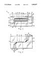
- FIG. 1is a schematic diagram of a Mach-Zehnder electro-optic modulator assembly embodying the present invention, illustrating optical and coplanar waveguides thereof to greatly enlarged scale;
- FIG. 2is a plan view illustrating a Chebyshev impedance transformer configuration of the present modulator assembly
- FIG. 3is a perspective view of the present modulator assembly
- FIG. 4is an exploded view of the present modulator assembly and a mechanical package for mounting the same.
- a travelling wave electro-optic modulator assembly based on a planar Mach-Zehnder interferometeris generally designated as 10, and includes a substrate 12 formed of a material such as lithium niobate which exhibits the required electro-optic effect.
- An optical waveguide 14is formed in the substrate 12 by a suitable process such as in-diffusion of titanium.
- the waveguide 14includes an optical input 16 for receiving an optical signal as a beam of light for modulation by a microwave frequency input signal, and an optical output 18 for connection with an optical fiber link or the like.
- the optical input signalis produced by a semiconductor laser or other appropriate source (not shown) at a preferred, but not limiting, wavelength of 1.3 ⁇ m.
- the waveguide 14further includes two branches 20 and 22, which diverge from the optical input 16 and extend generally parallel to each other.
- the branches 20 and 22converge at their other ends into the optical output 18.
- the branches 20 and 22have equal lengths.
- the modulator 10further includes an electrical coplanar waveguide 24 (in which the hot lead and ground plane are coplanar) for coupling an input microwave frequency electrical signal to the optical waveguide 14 to modulate the optical signal.
- the waveguide 24includes a center conductor 26 having an input section 28, a central section 30, and an output section 32.
- a larger outer conductor 34is provided around the center conductor 26, and electrically connected to a suitable reference potential such as ground.
- a suitable bias voltageis applied from a source (not shown) to the center conductor 26 to bias the modulator 10 at a linear operating point.
- the microwave signal applied to the center conductor 26causes the indices of refraction of the material in the branches 20 and 22 of the optical waveguide 14 to vary in an unequal manner due to the electro-optical effect in accordance with the index ellipsoid and trigonal crystal symmetry of the lithium niobate material, causing a differential in the phases of the signals propagating from the branches 20 and 22 into the optical output 18.
- Thiscauses interference between the optical signals from the branches 20 and 22 to an extent corresponding to the instantaneous potential of the microwave input signal, a corresponding variation in the energy of the optical signal at the optical output 18, and thereby amplitude modulation of the optical signal.
- a substrate 36made of a block of a material such as alumina on which is formed a conventional microstrip input line 38 typically having an impedance of 50 ⁇ .
- the adjacent edges of the substrates 12 and 36are butted together, and the microstrip line 38 electrically connected to the input section 28 of the coplanar waveguide center connector 26 by a gold bond ribbon 37.
- the outer conductor 34 of the waveguide 24is connected to a ground plane 39 of the microstrip line 38 by a gold bond ribbon 40 which is bent from the upper surface of the substrate 12 around the edge thereof to the lower surface of the substrate 36.
- a similar substrate 42, 50 ⁇ microstrip output line 44, ground plane 45, and gold bond ribbons 46 and 48are interconnected with the output section 32 of the waveguide center connector 26.
- impedance matching transformers fabricated on the electro-optic material substrateare provided between the microstrip lines 38 and 44, which typically have impedances of about 50 ⁇ , and the coplanar waveguide 24, which typically has an impedance on the order of 25 ⁇ .
- the waveguides 14 and 24are not visible in detail due to the scale of the drawing.
- the electro-optical interaction length of the modulatorwill typically be on the order of 3.5 mm, although this dimension does not limit of the scope of the invention.
- An input impedance matching transformer 50includes the input section 28 of the coplanar waveguide center conductor 26. Edges 52 and 54 of the input section 28 are shaped in relation to adjacent edges 56 and 58 of the outer conductor 34 of the coplanar waveguide 24 in such a manner that the characteristic impedance of the input section 28 smoothly transitions from 50 ⁇ to 25 ⁇ from the input end thereof which connects to the microstrip line 38, to the output end thereof which connects to the center section 30.
- a similar impedance matching transformer 60is provided at the output end of the center connector 26, including edges 62 and 64 of the output section 32 of the center conductor 26, and adjacent edges 66 and 68 of the outer conductor 34.
- the shapes of the edges 52, 54, 56, 58, 62, 64, 66 and 68are preferably designed such that the transformers 50 and 60 will form Chebyshev transformers.
- the characteristic impedance along the input section 28may be calculated as described in a paper entitled “A Transmission Line Taper of Improved Design", by R. Klopfenstein, in Proceedings of the IRE, 1956, pp. 31 to 35.
- the tapers of the edges as a function of characteristic impedancemay be calculated as described in a textbook entitled “Microstrip Lines and Slotlines", by K. Gurta, Artech House, 1979, p. 275.
- the actual dimensions of the edgeswill vary depending on the particular application, but may be calculated using the Chebyshev relationships in these references.
- the Chebyshev taper configurationhas been found to be optimum in that it has a minimum reflection coefficient in the pass band for a specified length of taper, and for a specified maximum magnitude reflection coefficient in the pass band, the taper has minimum length.
- a practical modulator arrangementhas been found to be feasible having a return loss on the order of 20 dB.
- Exemplary dimensions for the transformer 50 suitable for matching a 50 ⁇ microstrip line 38 to the 25 ⁇ coplanar waveguide 24 as described aboveare given in the following table, with the length of the centerline of the input section 28 from the microstrip line 38 to the central section 30 being 2723.7 ⁇ m. The length is divided into 21 equal increments of 129.7 ⁇ m each. The width W of the input section 28 between the edges 52 and 54, and the ground plane spacing D between the edges 56 and 58 of the outer conductor 34, are given in microns for each increment.
- the modulator substrate 12is mounted on a block 70 of microwave energy absorbing material using cement or other appropriate means.
- the block 70may preferably be made of a magnetically loaded epoxide material such as manufactured by the Emerson and Cumming Company under the tradename Eccosorb.
- the block 70absorbs spurious resonant microwave emissions resulting from a mismatch in the dielectric constant at the interface of the substrate 12 and the block 70 itself, as well as any undesired microstrip or other resonant modes generated in the apparatus 10. Reduction of spurious resonances to a negligible level through absorption thereof by the block enables the modulator to operate over a wide range of microwave input frequencies with smooth frequency response.
- Eccosorb MF-124 materialwhich has an insertion loss of 149 dB/cm at 18 GHz.
- the Eccosorb materialhas the advantage of being easily machinable into any desired shape.
- the scope of the inventionincludes the absorption of spurious resonant emissions using any suitable material.
- FIG. 4A rugged package for mounting the apparatus 10 for support and interconnection with standard optical link elements is illustrated in FIG. 4, and includes a block 72 made of a metal or other rigid, durable material.
- the block 70is designed to fit snugly into a deep groove 74 in the block 72 in which it is cemented or otherwise fixed in place.
- the substrates 36 and 42are cemented to portions 76 and 78 respectively of the block 72 on opposite sides of the groove 74.
- An input connector 80which preferably has a conventional 50 ⁇ SMA (small microwave connector, type A) configuration is fixed to a side plate 82 by means of a flange 84 and screws 86.
- the center lead of the connector 80is electrically connected to the input microstrip line 38 through a hole 88 in the side plate 82 by means of a gold bond ribbon or the like, although not visible in the drawing.
- An output connector 90is connected to the output microstrip line 44 by a similar arrangement, with the corresponding elements designated by the same reference numerals.
- the block 72is formed on its opposite sides with vertical grooves 92, which have shapes conjugate to vertical ridges 94 formed on the side plates 82, enabling the elements of the assembly 10 to be quickly joined together in precise alignment and fixed together with screws 96. Further illustrated are pressure ridges 98 and 100 formed on the block 72 to ensure good electrical contact between the microstrip ground planes and SMA ground.
Landscapes
- Physics & Mathematics (AREA)
- Nonlinear Science (AREA)
- Electromagnetism (AREA)
- General Physics & Mathematics (AREA)
- Optics & Photonics (AREA)
- Optical Modulation, Optical Deflection, Nonlinear Optics, Optical Demodulation, Optical Logic Elements (AREA)
- Optical Integrated Circuits (AREA)
Abstract
Description
TABLE ______________________________________ Point no. W D ______________________________________ Base 254 1419.8 1 242.5 1274.3 2 231 1137.9 3 219.5 1011.5 4 208 895 5 196.5 788.8 6 185 691.8 7 173.5 605.2 8 162 527 9 150.5 457.7 10 139 395.7 11 127.5 340.5 12 116 291.7 13 104.5 248.2 14 93 209.2 15 81.5 174.4 16 70 143 17 58.5 114.5 18 47 88.5 19 35.5 64.5 20 24 42.3End 24 36 ______________________________________
Claims (6)
Priority Applications (6)
| Application Number | Priority Date | Filing Date | Title |
|---|---|---|---|
| US07/502,377US5208697A (en) | 1990-03-30 | 1990-03-30 | Microwave frequency range electro-optic modulator with efficient input coupling and smooth wideband frequency response |
| GB9103351AGB2272979B (en) | 1990-03-30 | 1991-02-18 | Microwave frequency range electro-optic modulator with efficient input coupling and smooth wideband frequency response |
| DE4106993ADE4106993C2 (en) | 1990-03-30 | 1991-03-05 | Electro-optical modulator arrangement |
| SE9100689ASE9100689L (en) | 1990-03-30 | 1991-03-08 | Microwave frequency electro-optic modulator |
| ITRM910196AIT1250600B (en) | 1990-03-30 | 1991-03-26 | ELECTRO-OPTIC MODULATOR IN THE FIELD OF MICROWAVE FREQUENCIES WITH EFFICIENT INPUT COUPLING AND UNIFORM LARGE BAND FREQUENCY RESPONSE |
| FR9108802AFR2814249A1 (en) | 1990-03-30 | 1991-07-12 | Travelling-wave Mach-Zehnder electro-optic modulator |
Applications Claiming Priority (2)
| Application Number | Priority Date | Filing Date | Title |
|---|---|---|---|
| US07/502,377US5208697A (en) | 1990-03-30 | 1990-03-30 | Microwave frequency range electro-optic modulator with efficient input coupling and smooth wideband frequency response |
| FR9108802AFR2814249A1 (en) | 1990-03-30 | 1991-07-12 | Travelling-wave Mach-Zehnder electro-optic modulator |
Publications (1)
| Publication Number | Publication Date |
|---|---|
| US5208697Atrue US5208697A (en) | 1993-05-04 |
Family
ID=26228832
Family Applications (1)
| Application Number | Title | Priority Date | Filing Date |
|---|---|---|---|
| US07/502,377Expired - LifetimeUS5208697A (en) | 1990-03-30 | 1990-03-30 | Microwave frequency range electro-optic modulator with efficient input coupling and smooth wideband frequency response |
Country Status (6)
| Country | Link |
|---|---|
| US (1) | US5208697A (en) |
| DE (1) | DE4106993C2 (en) |
| FR (1) | FR2814249A1 (en) |
| GB (1) | GB2272979B (en) |
| IT (1) | IT1250600B (en) |
| SE (1) | SE9100689L (en) |
Cited By (31)
| Publication number | Priority date | Publication date | Assignee | Title |
|---|---|---|---|---|
| US5339369A (en)* | 1992-10-23 | 1994-08-16 | General Microwave Israel Corporation | High-speed external modulator |
| US5408544A (en)* | 1993-12-28 | 1995-04-18 | Fujitsu Limited | Optical modulator for producing a controllable chirp |
| US5455876A (en)* | 1992-10-23 | 1995-10-03 | General Microwave Israel Corporation | High-speed external integrated optical modulator |
| DE4431589A1 (en)* | 1994-09-05 | 1996-03-07 | Deutsche Telekom Ag | Integrated optical single side band modulator for microwave frequencies e.g. for data transmission systems |
| US5572610A (en)* | 1993-06-15 | 1996-11-05 | Nec Corporation | Waveguide-type optical device and impedance matching method thereof |
| US5712933A (en)* | 1994-02-24 | 1998-01-27 | Nec Corporation | Waveguide-type optical device |
| US5729378A (en)* | 1995-11-10 | 1998-03-17 | Kokusai Densin Denwa Kabusiki Kaisha | Optical device |
| US6192167B1 (en)* | 1998-07-24 | 2001-02-20 | Uniphase Telecommunications Products | Differential drive optical modulator |
| US6304685B1 (en)* | 2000-05-05 | 2001-10-16 | The United States Of America As Represented By The Secretary Of The Navy | Low drive voltage LiNbO3 intensity modulator with reduced electrode loss |
| US20030147575A1 (en)* | 2002-02-07 | 2003-08-07 | Fujitsu Limited | Optical modulator module and optical modulator |
| KR100425366B1 (en)* | 2000-10-27 | 2004-03-30 | 마츠시타 덴끼 산교 가부시키가이샤 | Optical signal transmission system and magneto-optical modulator designed to establish modulation over wide range for use in the same |
| US6737931B2 (en) | 2002-07-19 | 2004-05-18 | Agilent Technologies, Inc. | Device interconnects and methods of making the same |
| US20040264832A1 (en)* | 2001-11-16 | 2004-12-30 | Jungo Kondo | Optical waveguide device, and a travelling wave form optical modulator |
| US20050058385A1 (en)* | 2003-08-18 | 2005-03-17 | Hassan Tanbakuchi | Low-pass filter transmission line with integral electroabsorption modulator |
| EP1574894A1 (en)* | 2004-03-11 | 2005-09-14 | Avanex Corporation | System for reducing the electrical return loss of a lithium niobate travelling wave optical modulator with low characteristic impedance |
| US20070041143A1 (en)* | 2005-07-01 | 2007-02-22 | The Boeing Company | Apparatus, system, and method for lightning strike protection and verification of dielectric inserts |
| EP1752817A4 (en)* | 2004-05-18 | 2008-06-25 | Ngk Insulators Ltd | OPTICAL WAVEGUIDE DEVICE |
| US20080180340A1 (en)* | 2007-01-31 | 2008-07-31 | International Business Machines Corporation | Waveguide Coupling Devices |
| US20100054743A1 (en)* | 2005-12-01 | 2010-03-04 | John Heaton | Method and device for digitising an electrical signal |
| US20120051683A1 (en)* | 2010-08-30 | 2012-03-01 | Fujitsu Optical Components Limited | Optical modulator module |
| US20130343695A1 (en)* | 2012-05-15 | 2013-12-26 | Commissariat A L'energie Atomique Et Aux Energies Alternatives | Polarization splitting optical coupler |
| US20150063809A1 (en)* | 2013-08-29 | 2015-03-05 | Fujitsu Optical Components Limited | Optical module and optical transmitter |
| US20150078763A1 (en)* | 2013-09-13 | 2015-03-19 | Fujitsu Optical Components Limited | Optical module and optical transmitter |
| JP2015519547A (en)* | 2012-04-16 | 2015-07-09 | ライカ・ジオシステムズ・アクチェンゲゼルシャフトLeica Geosystems Ag | Electro-optic distance measuring device |
| US20150362823A1 (en)* | 2014-06-12 | 2015-12-17 | Fujitsu Optical Components Limited | Optical module and transmitting device |
| JP2016109941A (en)* | 2014-12-08 | 2016-06-20 | 富士通オプティカルコンポーネンツ株式会社 | Optical module |
| US10088733B2 (en)* | 2016-08-08 | 2018-10-02 | Acacia Communications, Inc. | Segmented traveling wave optical modulators and related methods |
| JP2018169592A (en)* | 2017-03-30 | 2018-11-01 | 住友大阪セメント株式会社 | Light control element module |
| US10133142B2 (en) | 2016-03-29 | 2018-11-20 | Acacia Communications, Inc. | Silicon modulators and related apparatus and methods |
| WO2023004112A1 (en)* | 2021-07-22 | 2023-01-26 | The Regents Of The University Of California | Integrated magneto-optical modulator |
| US12019349B2 (en) | 2020-05-15 | 2024-06-25 | Fujitsu Optical Components Limited | Optical device and optical transceiver using the same |
Citations (13)
| Publication number | Priority date | Publication date | Assignee | Title |
|---|---|---|---|---|
| US3944950A (en)* | 1972-01-19 | 1976-03-16 | The United States Of America As Represented By The Secretary Of The Army | Quasi-optical integrated circuits |
| US4205311A (en)* | 1977-09-14 | 1980-05-27 | Sony Corporation | Liquid crystal display device |
| US4208091A (en)* | 1977-03-30 | 1980-06-17 | United Technologies Corporation | Broadband microwave waveguide modulator for infrared lasers |
| EP0018150A1 (en)* | 1979-04-18 | 1980-10-29 | Magyar Tudomanyos Akademia Szamitastechnikai es Automatizalasi Kutato Intezete | Circuit arrangement for controlling a multi-beam acousto-optical cell |
| US4448479A (en)* | 1981-11-16 | 1984-05-15 | Bell Telephone Laboratories, Incorporated | Traveling wave, electrooptic devices with effective velocity matching |
| US4553810A (en)* | 1983-04-21 | 1985-11-19 | At&T Bell Laboratories | Traveling wave electrooptic devices |
| WO1987003383A1 (en)* | 1985-11-25 | 1987-06-04 | Eastman Kodak Company | Circuit for electro-optic modulators |
| US4679893A (en)* | 1983-08-26 | 1987-07-14 | Hughes Aircraft Company | High switching frequency optical waveguide switch, modulator, and filter devices |
| US4709978A (en)* | 1986-02-21 | 1987-12-01 | Bell Communications Research, Inc. | Mach-Zehnder integrated optical modulator |
| US4866406A (en)* | 1986-08-20 | 1989-09-12 | Sumitomo Special Metal Co., Ltd. | Wide-band optical modulator |
| US4917451A (en)* | 1988-01-19 | 1990-04-17 | E. I. Dupont De Nemours And Company | Waveguide structure using potassium titanyl phosphate |
| US4973140A (en)* | 1989-01-25 | 1990-11-27 | United Technologies Corporation | Reentrant traveling-wave single sideband optical modulator |
| US5005932A (en)* | 1989-11-06 | 1991-04-09 | Hughes Aircraft Company | Electro-optic modulator |
Family Cites Families (2)
| Publication number | Priority date | Publication date | Assignee | Title |
|---|---|---|---|---|
| DE3415523A1 (en)* | 1984-04-24 | 1985-10-24 | Beerwald, Hans, Dr.Rer.Nat., 5370 Kall | Device for shifting the frequency of infrared laser radiation by means of single-sideband modulation |
| FR2592966B1 (en)* | 1986-01-16 | 1989-11-10 | France Etat | DIRECT ELECTRO-OPTICAL COUPLER WITH PROGRESSIVE WAVE AND ALTERNATE PHASE. |
- 1990
- 1990-03-30USUS07/502,377patent/US5208697A/ennot_activeExpired - Lifetime
- 1991
- 1991-02-18GBGB9103351Apatent/GB2272979B/ennot_activeExpired - Fee Related
- 1991-03-05DEDE4106993Apatent/DE4106993C2/ennot_activeExpired - Fee Related
- 1991-03-08SESE9100689Apatent/SE9100689L/ennot_activeApplication Discontinuation
- 1991-03-26ITITRM910196Apatent/IT1250600B/enactiveIP Right Grant
- 1991-07-12FRFR9108802Apatent/FR2814249A1/enactivePending
Patent Citations (13)
| Publication number | Priority date | Publication date | Assignee | Title |
|---|---|---|---|---|
| US3944950A (en)* | 1972-01-19 | 1976-03-16 | The United States Of America As Represented By The Secretary Of The Army | Quasi-optical integrated circuits |
| US4208091A (en)* | 1977-03-30 | 1980-06-17 | United Technologies Corporation | Broadband microwave waveguide modulator for infrared lasers |
| US4205311A (en)* | 1977-09-14 | 1980-05-27 | Sony Corporation | Liquid crystal display device |
| EP0018150A1 (en)* | 1979-04-18 | 1980-10-29 | Magyar Tudomanyos Akademia Szamitastechnikai es Automatizalasi Kutato Intezete | Circuit arrangement for controlling a multi-beam acousto-optical cell |
| US4448479A (en)* | 1981-11-16 | 1984-05-15 | Bell Telephone Laboratories, Incorporated | Traveling wave, electrooptic devices with effective velocity matching |
| US4553810A (en)* | 1983-04-21 | 1985-11-19 | At&T Bell Laboratories | Traveling wave electrooptic devices |
| US4679893A (en)* | 1983-08-26 | 1987-07-14 | Hughes Aircraft Company | High switching frequency optical waveguide switch, modulator, and filter devices |
| WO1987003383A1 (en)* | 1985-11-25 | 1987-06-04 | Eastman Kodak Company | Circuit for electro-optic modulators |
| US4709978A (en)* | 1986-02-21 | 1987-12-01 | Bell Communications Research, Inc. | Mach-Zehnder integrated optical modulator |
| US4866406A (en)* | 1986-08-20 | 1989-09-12 | Sumitomo Special Metal Co., Ltd. | Wide-band optical modulator |
| US4917451A (en)* | 1988-01-19 | 1990-04-17 | E. I. Dupont De Nemours And Company | Waveguide structure using potassium titanyl phosphate |
| US4973140A (en)* | 1989-01-25 | 1990-11-27 | United Technologies Corporation | Reentrant traveling-wave single sideband optical modulator |
| US5005932A (en)* | 1989-11-06 | 1991-04-09 | Hughes Aircraft Company | Electro-optic modulator |
Non-Patent Citations (28)
| Title |
|---|
| Betts et al.; "High Sensitivity . . . in LiNbO3"; Jnl. of Lightwave Tech., vol. 7, #12, pp. 2078-2083, Dec. 1989, abst. |
| Betts et al.; High Sensitivity . . . in LiNbO 3 ; Jnl. of Lightwave Tech., vol. 7, 12, pp. 2078 2083, Dec. 1989, abst.* |
| Conference Paper of 23rd International Congress on Electronics, published 1976, Italy, pp. 161 166, Electrooptical Modulator Using Microstrip Lines as Matching Networks , V. Andresciani et al.* |
| Conference Paper of 23rd International Congress on Electronics, published 1976, Italy, pp. 161-166, "Electrooptical Modulator Using Microstrip Lines as Matching Networks", V. Andresciani et al. |
| Cross et al., "Microwave Integrated Optical Modulator", Appl. Phys. Lett. 44(5), 1 Mar. 1984, pp. 486-488. |
| Cross et al., Microwave Integrated Optical Modulator , Appl. Phys. Lett. 44(5), 1 Mar. 1984, pp. 486 488.* |
| Dolfi, "Traveling-wave 1.3-μm Interferometer Modulator with High Bandwidth, Low Drive Power, and Low Loss", Applied Optics, vol. 25, No. 15, 1 Aug. 1986, pp. 2479-2480. |
| Dolfi, Traveling wave 1.3 m Interferometer Modulator with High Bandwidth, Low Drive Power, and Low Loss , Applied Optics, vol. 25, No. 15, 1 Aug. 1986, pp. 2479 2480.* |
| Gee et al., "Traveling-Wave Electrooptic Modulator", Applied Optics, vol. 22, No. 13, 1 Jul. 1983, pp. 2034-2037. |
| Gee et al., Traveling Wave Electrooptic Modulator , Applied Optics, vol. 22, No. 13, 1 Jul. 1983, pp. 2034 2037.* |
| Gibson et al., "Performance of High Frequency LiNbO3 Fibre Pigtailed Mach-Zehnder Waveguide Intensity Modulators at 1.32 μm and 1.52 μm", Pilkington Guided Wave Optics, Barr and Stroud Ltd., Glasgow, Scotland. |
| Gibson et al., Performance of High Frequency LiNbO 3 Fibre Pigtailed Mach Zehnder Waveguide Intensity Modulators at 1.32 m and 1.52 m , Pilkington Guided Wave Optics, Barr and Stroud Ltd., Glasgow, Scotland.* |
| Gupta et al., "Microstrip Lines and Slotlines", Artech House, 1979, p. 275. |
| Gupta et al., Microstrip Lines and Slotlines , Artech House, 1979, p. 275.* |
| Izutsu et al., "10 GHz Bandwidth Traveling-Wave LiNbO3 Optical Waveguide Modulator", IEEE Journal of Quantum Electronics, vol. QE-14, No. 6, Jun. 1978, pp. 394-395. |
| Izutsu et al., 10 GHz Bandwidth Traveling Wave LiNbO 3 Optical Waveguide Modulator , IEEE Journal of Quantum Electronics, vol. QE 14, No. 6, Jun. 1978, pp. 394 395.* |
| J. H. Schaffner; "Analysis of a Millimeter . . . Periodic Electrode"; SPIE Proc. OSP-Pat, Jan. 17, 1990, L.A., Calif., pp. 101-110. |
| J. H. Schaffner; Analysis of a Millimeter . . . Periodic Electrode ; SPIE Proc. OSP Pat, Jan. 17, 1990, L.A., Calif., pp. 101 110.* |
| Jalinsen et al.; "Integrated Optical Modulator . . ."; MFOC 1988 West Proc., Dec. 8, 1988, pp. 93-95; abst. only. |
| Jalinsen et al.; Integrated Optical Modulator . . . ; MFOC 1988 West Proc., Dec. 8, 1988, pp. 93 95; abst. only.* |
| Klopfenstein, "A Transmission Line Taper of Improved Design", Proceedings of the IRE, pp. 31-35. |
| Klopfenstein, A Transmission Line Taper of Improved Design , Proceedings of the IRE, pp. 31 35.* |
| Nick Parsons; "Integrated Optics", Artech House, Inc., 1989; Principals of Modern Optical Systems. |
| Nick Parsons; Integrated Optics , Artech House, Inc., 1989; Principals of Modern Optical Systems.* |
| Soo et al.; "A Study on the New Microstrip Magic Tee"; J. Korea Inst. Electron. Eng., vol. 17, #3, pp. 36-44, Jun. 1980, abst only. |
| Soo et al.; A Study on the New Microstrip Magic Tee ; J. Korea Inst. Electron. Eng., vol. 17, 3, pp. 36 44, Jun. 1980, abst only.* |
| SPIE, Optoelectronic Signal Processing for Phased Array Antennas II, vol. 1217 Jan. 1990, Analysis of a millimeter wave integrated electro optic modulator with a periodic electrode , J. H. Schaffner.* |
| SPIE, Optoelectronic Signal Processing for Phased-Array Antennas II, vol. 1217 Jan. 1990, "Analysis of a millimeter wave integrated electro-optic modulator with a periodic electrode", J. H. Schaffner. |
Cited By (50)
| Publication number | Priority date | Publication date | Assignee | Title |
|---|---|---|---|---|
| US5455876A (en)* | 1992-10-23 | 1995-10-03 | General Microwave Israel Corporation | High-speed external integrated optical modulator |
| US5339369A (en)* | 1992-10-23 | 1994-08-16 | General Microwave Israel Corporation | High-speed external modulator |
| US5572610A (en)* | 1993-06-15 | 1996-11-05 | Nec Corporation | Waveguide-type optical device and impedance matching method thereof |
| US5408544A (en)* | 1993-12-28 | 1995-04-18 | Fujitsu Limited | Optical modulator for producing a controllable chirp |
| US5712933A (en)* | 1994-02-24 | 1998-01-27 | Nec Corporation | Waveguide-type optical device |
| DE4431589C2 (en)* | 1994-09-05 | 1999-06-17 | Deutsche Telekom Ag | Integrated optical single-sideband modulator for microwave frequencies |
| DE4431589A1 (en)* | 1994-09-05 | 1996-03-07 | Deutsche Telekom Ag | Integrated optical single side band modulator for microwave frequencies e.g. for data transmission systems |
| US5729378A (en)* | 1995-11-10 | 1998-03-17 | Kokusai Densin Denwa Kabusiki Kaisha | Optical device |
| EP0773464A3 (en)* | 1995-11-10 | 1998-04-08 | Kokusai Denshin Denwa Kabushiki Kaisha | Optical device |
| US6192167B1 (en)* | 1998-07-24 | 2001-02-20 | Uniphase Telecommunications Products | Differential drive optical modulator |
| US6304685B1 (en)* | 2000-05-05 | 2001-10-16 | The United States Of America As Represented By The Secretary Of The Navy | Low drive voltage LiNbO3 intensity modulator with reduced electrode loss |
| KR100425366B1 (en)* | 2000-10-27 | 2004-03-30 | 마츠시타 덴끼 산교 가부시키가이샤 | Optical signal transmission system and magneto-optical modulator designed to establish modulation over wide range for use in the same |
| US7035485B2 (en)* | 2001-11-16 | 2006-04-25 | Ngk Insulators, Ltd. | Optical waveguide device, and a travelling wave form optical modulator |
| US20040264832A1 (en)* | 2001-11-16 | 2004-12-30 | Jungo Kondo | Optical waveguide device, and a travelling wave form optical modulator |
| EP1341027A3 (en)* | 2002-02-07 | 2003-09-17 | Fujitsu Limited | Optical modulator module and optical modulator |
| US6873748B2 (en) | 2002-02-07 | 2005-03-29 | Fujitsu Limited | Optical modulator module and optical modulator |
| US20030147575A1 (en)* | 2002-02-07 | 2003-08-07 | Fujitsu Limited | Optical modulator module and optical modulator |
| EP1995624A1 (en)* | 2002-02-07 | 2008-11-26 | Fujitsu Limited | Optical modulator module |
| US6737931B2 (en) | 2002-07-19 | 2004-05-18 | Agilent Technologies, Inc. | Device interconnects and methods of making the same |
| US20050058385A1 (en)* | 2003-08-18 | 2005-03-17 | Hassan Tanbakuchi | Low-pass filter transmission line with integral electroabsorption modulator |
| US7031558B2 (en) | 2003-08-18 | 2006-04-18 | Hassan Tanbakuchi | Low-pass filter transmission line with integral electroabsorption modulator |
| EP1574894A1 (en)* | 2004-03-11 | 2005-09-14 | Avanex Corporation | System for reducing the electrical return loss of a lithium niobate travelling wave optical modulator with low characteristic impedance |
| US20050201653A1 (en)* | 2004-03-11 | 2005-09-15 | Avanex Corporation | System for reducing the electrical return loss of a lithium niobate traveling wave optical modulator with low characteristic impedance |
| US7228014B2 (en) | 2004-03-11 | 2007-06-05 | Avanex Corporation | System for reducing the electrical return loss of a lithium niobate traveling wave optical modulator with low characteristic impedance |
| EP1752817A4 (en)* | 2004-05-18 | 2008-06-25 | Ngk Insulators Ltd | OPTICAL WAVEGUIDE DEVICE |
| US20070041143A1 (en)* | 2005-07-01 | 2007-02-22 | The Boeing Company | Apparatus, system, and method for lightning strike protection and verification of dielectric inserts |
| US7633283B2 (en)* | 2005-07-01 | 2009-12-15 | The Boeing Company | Method for lightning strike protection and verification of magnetizable dielectric inserts |
| US20100054743A1 (en)* | 2005-12-01 | 2010-03-04 | John Heaton | Method and device for digitising an electrical signal |
| US20080180340A1 (en)* | 2007-01-31 | 2008-07-31 | International Business Machines Corporation | Waveguide Coupling Devices |
| US20120051683A1 (en)* | 2010-08-30 | 2012-03-01 | Fujitsu Optical Components Limited | Optical modulator module |
| JP2012048121A (en)* | 2010-08-30 | 2012-03-08 | Fujitsu Optical Components Ltd | Optical modulator module |
| US8712195B2 (en)* | 2010-08-30 | 2014-04-29 | Fujitsu Optical Components Limited | Optical modulator module |
| USRE46932E1 (en)* | 2010-08-30 | 2018-07-03 | Fujitsu Optical Components Limited | Optical modulator module |
| JP2015519547A (en)* | 2012-04-16 | 2015-07-09 | ライカ・ジオシステムズ・アクチェンゲゼルシャフトLeica Geosystems Ag | Electro-optic distance measuring device |
| US9405007B2 (en) | 2012-04-16 | 2016-08-02 | Leica Geosystems Ag | Electro-optic distance-measuring device |
| US20130343695A1 (en)* | 2012-05-15 | 2013-12-26 | Commissariat A L'energie Atomique Et Aux Energies Alternatives | Polarization splitting optical coupler |
| US9134482B2 (en)* | 2012-05-15 | 2015-09-15 | Commissariat à l'énergie atmoique aux énergies alternatives | Polarization splitting optical coupler having an interposed guide segment extending between first and second coplanar waveguides |
| US20150063809A1 (en)* | 2013-08-29 | 2015-03-05 | Fujitsu Optical Components Limited | Optical module and optical transmitter |
| US9231728B2 (en)* | 2013-08-29 | 2016-01-05 | Fujitsu Optical Components Limited | Optical module and optical transmitter |
| US20150078763A1 (en)* | 2013-09-13 | 2015-03-19 | Fujitsu Optical Components Limited | Optical module and optical transmitter |
| US9229292B2 (en)* | 2013-09-13 | 2016-01-05 | Fujitsu Optical Components Limited | Optical module and optical transmitter |
| US20150362823A1 (en)* | 2014-06-12 | 2015-12-17 | Fujitsu Optical Components Limited | Optical module and transmitting device |
| US9709871B2 (en)* | 2014-06-12 | 2017-07-18 | Fujitsu Optical Components Limited | Optical module and transmitting device |
| JP2016001284A (en)* | 2014-06-12 | 2016-01-07 | 富士通オプティカルコンポーネンツ株式会社 | Optical module and transmitter |
| JP2016109941A (en)* | 2014-12-08 | 2016-06-20 | 富士通オプティカルコンポーネンツ株式会社 | Optical module |
| US10133142B2 (en) | 2016-03-29 | 2018-11-20 | Acacia Communications, Inc. | Silicon modulators and related apparatus and methods |
| US10088733B2 (en)* | 2016-08-08 | 2018-10-02 | Acacia Communications, Inc. | Segmented traveling wave optical modulators and related methods |
| JP2018169592A (en)* | 2017-03-30 | 2018-11-01 | 住友大阪セメント株式会社 | Light control element module |
| US12019349B2 (en) | 2020-05-15 | 2024-06-25 | Fujitsu Optical Components Limited | Optical device and optical transceiver using the same |
| WO2023004112A1 (en)* | 2021-07-22 | 2023-01-26 | The Regents Of The University Of California | Integrated magneto-optical modulator |
Also Published As
| Publication number | Publication date |
|---|---|
| ITRM910196A0 (en) | 1991-03-26 |
| DE4106993A1 (en) | 1995-01-05 |
| GB2272979A (en) | 1994-06-01 |
| FR2814249A1 (en) | 2002-03-22 |
| GB9103351D0 (en) | 1994-03-02 |
| IT1250600B (en) | 1995-04-21 |
| ITRM910196A1 (en) | 1992-09-26 |
| GB2272979B (en) | 1994-09-14 |
| SE9100689L (en) | 1995-07-20 |
| DE4106993C2 (en) | 1999-07-22 |
Similar Documents
| Publication | Publication Date | Title |
|---|---|---|
| US5208697A (en) | Microwave frequency range electro-optic modulator with efficient input coupling and smooth wideband frequency response | |
| US6483953B1 (en) | External optical modulation using non-co-linear compensation networks | |
| KR950000406B1 (en) | All-optical modulator and optical signal modulation method | |
| EP1335238B1 (en) | Optical phase modulator with electrode arrangement having a wideband transmission response | |
| US6504640B2 (en) | Resonant optical modulators with zero chirp | |
| US4208091A (en) | Broadband microwave waveguide modulator for infrared lasers | |
| US6909817B2 (en) | Electro-optic modulators with internal impedance matching | |
| AU9158798A (en) | Narrow-band optical modulator with reduced power requirement | |
| US6356673B1 (en) | Low loss coplanar waveguide horn for low drive LiNbO3 modulators | |
| JP3841933B2 (en) | Optical waveguide module | |
| US6016198A (en) | Electro-optic reflection device with traveling-wave structure | |
| CN101501555A (en) | Optical modulator | |
| US7016554B2 (en) | Optical modulator | |
| JP3043614B2 (en) | Waveguide type optical device | |
| NOGUCHI et al. | Push-pull type ridged Ti: LiNbO 3 optical modulator | |
| JP4443932B2 (en) | Conversion between optical and radio frequency signals | |
| Jiang et al. | LiNbO 3 Mach-Zehnder modulators with fixed negative chirp | |
| US7877015B2 (en) | Optical to radio frequency detector | |
| CN119644648B (en) | Large-bandwidth low-insertion-loss Mach-Zehnder modulator based on thin film lithium niobate | |
| Thylen et al. | High speed LiNbO3 integrated optics modulators and switches | |
| JPH04243217A (en) | light modulator | |
| US3653744A (en) | Optical modulator utilizing a slow wave circuit | |
| Knoesen et al. | High-bandwidth polymer in-line fiber modulator | |
| Perlmutter et al. | Symmetric Coplanar Electrodes For High Speed Ti: LiNbO3 Devices | |
| HK1075498B (en) | Conversion between optical and radio frequency signals |
Legal Events
| Date | Code | Title | Description |
|---|---|---|---|
| AS | Assignment | Owner name:HUGHES AIRCRAFT COMPANY, LOS ANGELES, CA A DE CORP Free format text:ASSIGNMENT OF ASSIGNORS INTEREST.;ASSIGNORS:SCHAFFNER, JAMES H.;JOYCE, ROBERT L.;REEL/FRAME:005266/0743 Effective date:19900314 Owner name:HUGHES AIRCRAFT COMPANY, LOS ANGELES, CA A CORP. O Free format text:ASSIGNMENT OF ASSIGNORS INTEREST.;ASSIGNOR:SCHELLENBERG, JAMES M.;REEL/FRAME:005266/0748 Effective date:19900324 Owner name:HUGHES AIRCRAFT COMPANY, LOS ANGELES, CA A DE CORP Free format text:ASSIGNMENT OF ASSIGNORS INTEREST.;ASSIGNOR:GEE, CAROLINE M.;REEL/FRAME:005266/0746 Effective date:19900316 | |
| STCF | Information on status: patent grant | Free format text:PATENTED CASE | |
| FEPP | Fee payment procedure | Free format text:PAYOR NUMBER ASSIGNED (ORIGINAL EVENT CODE: ASPN); ENTITY STATUS OF PATENT OWNER: LARGE ENTITY | |
| REMI | Maintenance fee reminder mailed | ||
| FPAY | Fee payment | Year of fee payment:4 | |
| SULP | Surcharge for late payment | ||
| AS | Assignment | Owner name:HUGHES ELECTRONICS CORPORATION, CALIFORNIA Free format text:ASSIGNMENT OF ASSIGNORS INTEREST;ASSIGNOR:HE HOLDINGS INC., HUGHES ELECTRONICS FORMERLY KNOWN AS HUGHES AIRCRAFT COMPANY;REEL/FRAME:009350/0366 Effective date:19971217 | |
| FEPP | Fee payment procedure | Free format text:PAYER NUMBER DE-ASSIGNED (ORIGINAL EVENT CODE: RMPN); ENTITY STATUS OF PATENT OWNER: LARGE ENTITY Free format text:PAYOR NUMBER ASSIGNED (ORIGINAL EVENT CODE: ASPN); ENTITY STATUS OF PATENT OWNER: LARGE ENTITY | |
| FPAY | Fee payment | Year of fee payment:8 | |
| FPAY | Fee payment | Year of fee payment:12 |