US5208568A - Method for producing dielectric resonator apparatus having metallized mesa - Google Patents
Method for producing dielectric resonator apparatus having metallized mesaDownload PDFInfo
- Publication number
- US5208568A US5208568AUS07/829,367US82936792AUS5208568AUS 5208568 AUS5208568 AUS 5208568AUS 82936792 AUS82936792 AUS 82936792AUS 5208568 AUS5208568 AUS 5208568A
- Authority
- US
- United States
- Prior art keywords
- protuberance
- hole
- dielectric
- mesa
- block
- Prior art date
- Legal status (The legal status is an assumption and is not a legal conclusion. Google has not performed a legal analysis and makes no representation as to the accuracy of the status listed.)
- Expired - Lifetime
Links
Images
Classifications
- H—ELECTRICITY
- H01—ELECTRIC ELEMENTS
- H01P—WAVEGUIDES; RESONATORS, LINES, OR OTHER DEVICES OF THE WAVEGUIDE TYPE
- H01P11/00—Apparatus or processes specially adapted for manufacturing waveguides or resonators, lines, or other devices of the waveguide type
- H01P11/008—Manufacturing resonators
- H—ELECTRICITY
- H01—ELECTRIC ELEMENTS
- H01P—WAVEGUIDES; RESONATORS, LINES, OR OTHER DEVICES OF THE WAVEGUIDE TYPE
- H01P1/00—Auxiliary devices
- H01P1/20—Frequency-selective devices, e.g. filters
- H01P1/201—Filters for transverse electromagnetic waves
- H01P1/205—Comb or interdigital filters; Cascaded coaxial cavities
- H01P1/2056—Comb filters or interdigital filters with metallised resonator holes in a dielectric block
- H—ELECTRICITY
- H01—ELECTRIC ELEMENTS
- H01P—WAVEGUIDES; RESONATORS, LINES, OR OTHER DEVICES OF THE WAVEGUIDE TYPE
- H01P7/00—Resonators of the waveguide type
- H01P7/04—Coaxial resonators
- Y—GENERAL TAGGING OF NEW TECHNOLOGICAL DEVELOPMENTS; GENERAL TAGGING OF CROSS-SECTIONAL TECHNOLOGIES SPANNING OVER SEVERAL SECTIONS OF THE IPC; TECHNICAL SUBJECTS COVERED BY FORMER USPC CROSS-REFERENCE ART COLLECTIONS [XRACs] AND DIGESTS
- Y10—TECHNICAL SUBJECTS COVERED BY FORMER USPC
- Y10T—TECHNICAL SUBJECTS COVERED BY FORMER US CLASSIFICATION
- Y10T29/00—Metal working
- Y10T29/49—Method of mechanical manufacture
- Y10T29/49002—Electrical device making
- Y10T29/49016—Antenna or wave energy "plumbing" making
Definitions
- This inventionrelates generally to electrical signal filters, and in particular to so-called ceramic, or dielectric, resonators and filters.
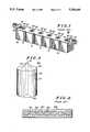
- Prior art ceramic bandpass filterssuch as that shown in FIG. 1 and described in U.S. Pat. No. 4,431,977, are typically constructed from blocks of ceramic material.
- the blocksare typically formed by pressing a ceramic-based powder, using a mold or other equivalent, to form a solid structure. The resulting structure may then be cured, or fired, to form a rigid block of ceramic.
- the blockincluding any number of through holes (e.g., holes 140 shown in FIG. 1) which make up the individual resonator structures, is then selectively coated with a conductive metallization layer. The coating is typically applied to the block so as to provide a shorted, typically one-quarter wavelength, transmission line resonator with each of the holes. Further processing of the metallization, as next described, is required to tune the resonator/filter to the desired frequency characteristics.
- FIG. 2shows a top view of a prior art ceramic block filter having an intricate metallization pattern on the top surface.
- the filter 200is described in U.S. Pat. No. 4,692,726 (issued to Green et al. on Sep. 8, 1987, and assigned to the assignee of the present invention).
- the metallization pattern on the top surface of a dielectric filteris commonly known to affect the capacitive loading on the top surface of the dielectric filter.
- the patternmay be made up of a ground plane coating (203), input/output pads (201), and various resonator pads (202, 204) which surround the hole resonators.
- the capacitive loading at the top of the blockcan be altered. Altering the capacitive top loading is a well-known method for frequency tuning dielectric resonators and filters, as the capacitive reactance plays a significant role in the overall frequency response characteristics (i.e. center frequency, bandwidth, etc.).
- Detailed metallization patternslike the one shown in FIG. 2 are typically screen printed, e.g., using a plating mask or similar article, onto the top surface of the block.
- the results of this processhave proven to be greatly dependent on the registration of the block with respect to the plating mask. That is, even a slight mis-alignment between the mask and the block often results in a resonator which is either unusable, or one that needs a substantial amount of tuning to meet the required specifications.
- Most tuning techniques todayinvolve removing portions of the metallized top-patterns, which operations are often manual (e.g., using a hand-held grinding tool).
- the present inventionencompasses a dielectric resonator which is formed from a block of dielectric material having top, bottom, and side surfaces.
- a protuberanceis formed on at least the top surface of the block.
- a holeis formed through the block, which hole extends substantially from the apex of the protuberance, through the block, to the bottom surface.
- the hole and protuberancecombine to form a mesa structure.
- the bottom surface, side surface, and an interior surface of the holeare coated with a conductive layer.
- a conductive coatingis selectively disposed on the top surface of the block, which coating at least partially covers the mesa.
- a dielectric block resonatoris thereby formed whose resonant characteristics are at least partially determined by the physical dimensions of the mesa.
- FIG. 1is an isometric view of a dielectric block filter which is known in the prior art.
- FIG. 2is a top view showing the metallization pattern on one surface of dielectric filter, which filter is known in the prior art.
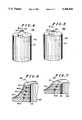
- FIG. 3is an isometric view of a ceramic structure, which may be used in accordance with the present invention.
- FIG. 4is an isometric view of the structure of FIG. 3 after further processing, in accordance with the present invention.
- FIG. 5is an isometric view of the structure of FIG. 4 after still further processing, in accordance with the present invention.
- FIG. 6is an isometric cross-sectional view of a portion of the structure of FIG. 4, in accordance with the present invention.
- FIG. 7is an isometric cross-sectional view of a portion of the structure of FIG. 5, in accordance with the present invention.
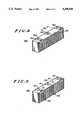
- FIG. 8is an isometric view of a dielectric filter, in accordance with one embodiment of the present invention.
- FIG. 9is an isometric view of a dielectric filter, in accordance with an alternate embodiment of the present invention.
- FIG. 3shows a ceramic structure 300, having a protuberance 304 formed on the top surface thereof, in accordance with one embodiment of the invention.
- protuberance 304is formed from the same material as the block, but it may be formed of any suitable dielectric material.
- the structure 300also includes a hole 305, which is preferably centered at the apex of the protuberance 304. Hole 305 extends through the apex of the protuberance 304, through the ceramic structure, to the bottom surface 302. Hole 305 further has an interior surface 306, which is substantially parallel with exterior surface 301 as shown. (The physical dimensions of the protuberance 304 will, as later described, be altered to affect an electrical tuning of the resonator during manufacture.)
- Processing a ceramic block resonator from the structure shown in FIG. 3requires the application of a conductive layer to at least some portions of the block.
- the entire structureincluding all sides (301-303), protuberance 304, and interior surface 306 of hole 305, is coated with a conductive paste.
- the conductive pastee.g., silver-glass paste such as Cermalloy C8710 is then cured to form a conductive metallization layer over the entire block. Further processing of the coated ceramic structure, as next described, will enable the coated structure to perform as a transmission line resonator, which performance is well established in the art.
- ceramic resonators of this typeare familiar with a physical grinding, (e.g., lapping, milling) process which is typically used to correct malformed blocks.
- the blockmay be somewhat misshaped, e.g., having concave or convex sides.
- the uncoated blocksare milled or lapped; a well known process which typically involves passing the surface to be corrected across an abrasive surface in order to remove undesired material.
- a milling processmay be used to provide an electrical discontinuity, or gap, between the inner surface 306 and the conductive sides of the protuberance 304.
- This gap in the metallization layeris required for the structure to behave like a transmission line resonator, and is provided by removing a top portion of the protuberance 304, as well as the metallization disposed thereon, as next described.
- FIG. 4shows a ceramic structure, such as the one shown in FIG. 3, which is coated with a conductive metallization layer and then milled in accordance with the invention.
- Milling protuberance 407 across a horizontal planei.e. parallel to the top and bottom surfaces of the block) removes the metallization on the upper portion of the structure.
- the desired gapis thereby created between the metallized interior surface 406 of hole 405, and the metallized side surface of protuberance 407.
- further grindingreduces the height of the protuberance 407, which alters the capacitive reactance between these two metallized surfaces, as later described.
- FIG. 6there is shown a partial cross-sectional view of the dielectric resonator 400 shown in FIG. 4, which view shows the mesa-like structure 604 formed after milling the protuberance 407.
- This mesacan be formed to have varying physical dimensions (i.e., height, width, surface areas, etc.), which physical dimensions play an important role in the resonant characteristics of the resonator.
- Milling through the metallization on the top of the mesaproduces a capacitance between metallized layers 406 and 407 (i.e. approximating a simple parallel-plate capacitor) which capacitance is represented by reference numbers 602A-D.
- FIG. 7shows a partial cross-sectional view of the top surface of resonator 500 shown in FIG. 5, which is formed by further milling the resonator 400 shown in FIG. 4.
- Capacitors 702A-Brepresent the effective capacitance between metallized interior surface 506 of hole 505 and the metallized protuberance 507. As mentioned earlier, altering the capacitance in this way results in predictable changes in the frequency response of the resonator. Therefore, by milling the surface of the protuberance 701, a method is provided for easily adjusting the frequency characteristics of the resonator. Accordingly, the (capacitive) top loading of the resonator can be altered by simply milling more or less material from the protuberance disposed on the top surface of the resonator.
- resonator structuresin parallel. These resonators may be integrally disposed within the same ceramic block or they may be independent structures, each having their own resonance characteristics. Dielectric filters are often constructed by forming dielectric resonators, and placing them in parallel, on the same dielectric block. Further, altering the capacitive top loading of such structures results in changes in the capacitive coupling between each resonator (thus changing the response characteristics of the filter).
- FIG. 8shows a dielectric resonator filter, or so-called combline filter, which employs the present invention.
- Filter 800shows a parallelepiped ceramic block having three holes formed therethrough. The three holes 805, 806, 807 are separated by a distance 801, which distance affects the amount of inter-resonator coupling (this relationship is well understood in the art).
- the region 803 of the block between resonators 805, 806, 807is coated with a conductive layer. Alternatively, region 803 may be selectively coated to alter the inter-resonator coupling, which in turn affects the frequency response characteristics of the filter (i.e. center frequency, transmission zeroes, bandwidth, etc.).
- Surface 809i.e.
- an unmetallized annular region around hole 805 created by the milling process described hereinacts as a dielectric gap between the metallized hole 805 and the metallized sides of the mesa.
- surface 809is shown to be concentric with the resonator hole, but may vary in shape with respect to the hole to allow design flexibility. The relationship between the hole shape (e.g., round, square, elliptic, etc.) and the shape of the metallization around the hole is well known in the art and is therefore not addressed here.
- FIG. 9shows an alternate embodiment of the present invention, which embodiment is in the form of an interdigital filter 900.
- Inter-digital filterswhose response characteristics are well established in the art, are similar to the aforementioned combline structure except that alternating resonator sections are physically inverted within the block. That is, resonators 901, interposed among resonators 905-907 are inverted with respect to these resonators. Accordingly, the so-called top loading of resonators 901 is altered by processing protuberances 902 (located on the "bottom" of the dielectric block) with a metallization and milling operation similar to the one described above for the resonators and combline filter.
Landscapes
- Physics & Mathematics (AREA)
- Electromagnetism (AREA)
- Engineering & Computer Science (AREA)
- Manufacturing & Machinery (AREA)
- Control Of Motors That Do Not Use Commutators (AREA)
Abstract
Description
Claims (5)
Priority Applications (1)
| Application Number | Priority Date | Filing Date | Title |
|---|---|---|---|
| US07/829,367US5208568A (en) | 1992-02-03 | 1992-02-03 | Method for producing dielectric resonator apparatus having metallized mesa |
Applications Claiming Priority (1)
| Application Number | Priority Date | Filing Date | Title |
|---|---|---|---|
| US07/829,367US5208568A (en) | 1992-02-03 | 1992-02-03 | Method for producing dielectric resonator apparatus having metallized mesa |
Publications (1)
| Publication Number | Publication Date |
|---|---|
| US5208568Atrue US5208568A (en) | 1993-05-04 |
Family
ID=25254340
Family Applications (1)
| Application Number | Title | Priority Date | Filing Date |
|---|---|---|---|
| US07/829,367Expired - LifetimeUS5208568A (en) | 1992-02-03 | 1992-02-03 | Method for producing dielectric resonator apparatus having metallized mesa |
Country Status (1)
| Country | Link |
|---|---|
| US (1) | US5208568A (en) |
Cited By (7)
| Publication number | Priority date | Publication date | Assignee | Title |
|---|---|---|---|---|
| US5327109A (en)* | 1992-11-04 | 1994-07-05 | Motorola, Inc. | Block filter having high-side passband transfer function zeroes |
| WO1995030249A1 (en)* | 1994-04-29 | 1995-11-09 | Motorola Inc. | An improved method of tuning a ceramic duplex filter |
| US20030134539A1 (en)* | 2000-08-18 | 2003-07-17 | Eagle Comtronics, Inc. | Electrical signal filter housing with hexagonal drive section |
| US20040174236A1 (en)* | 2002-02-21 | 2004-09-09 | Matthews Brian Richard | Ceramic RF filter having improved third harmonic response |
| US20090315642A1 (en)* | 2006-07-25 | 2009-12-24 | Koninklijke Philips Electronics N. V. | Moulded cable traps |
| US20100062215A1 (en)* | 2008-09-09 | 2010-03-11 | Hitachi Maxell, Ltd. | Component having through-hole and method of manufacturing component |
| US10312563B2 (en)* | 2016-11-08 | 2019-06-04 | LGS Innovations LLC | Ceramic filter with differential conductivity |
Citations (10)
| Publication number | Priority date | Publication date | Assignee | Title |
|---|---|---|---|---|
| US4431977A (en)* | 1982-02-16 | 1984-02-14 | Motorola, Inc. | Ceramic bandpass filter |
| US4506241A (en)* | 1981-12-01 | 1985-03-19 | Matsushita Electric Industrial Co., Ltd. | Coaxial dielectric resonator having different impedance portions and method of manufacturing the same |
| JPS6243904A (en)* | 1985-08-22 | 1987-02-25 | Murata Mfg Co Ltd | Dielectric resonator |
| US4668925A (en)* | 1984-11-17 | 1987-05-26 | Tdk Corporation | Dielectric resonator and method for making |
| US4692726A (en)* | 1986-07-25 | 1987-09-08 | Motorola, Inc. | Multiple resonator dielectric filter |
| JPS64801A (en)* | 1986-12-27 | 1989-01-05 | Nippon Chiyoutanpa Kk | Cl circuit element and series resonance type band stop filter |
| US4837534A (en)* | 1988-01-29 | 1989-06-06 | Motorola, Inc. | Ceramic block filter with bidirectional tuning |
| US4937542A (en)* | 1988-11-16 | 1990-06-26 | Alps Electric Co., Ltd. | Dielectric filter |
| JPH0321701A (en)* | 1989-06-17 | 1991-01-30 | Fujikura Ltd | Heater buried road |
| US5004992A (en)* | 1990-05-25 | 1991-04-02 | Motorola, Inc. | Multi-resonator ceramic filter and method for tuning and adjusting the resonators thereof |
- 1992
- 1992-02-03USUS07/829,367patent/US5208568A/ennot_activeExpired - Lifetime
Patent Citations (11)
| Publication number | Priority date | Publication date | Assignee | Title |
|---|---|---|---|---|
| US4506241A (en)* | 1981-12-01 | 1985-03-19 | Matsushita Electric Industrial Co., Ltd. | Coaxial dielectric resonator having different impedance portions and method of manufacturing the same |
| US4506241B1 (en)* | 1981-12-01 | 1993-04-06 | Matsushita Electric Industrial Co Ltd | |
| US4431977A (en)* | 1982-02-16 | 1984-02-14 | Motorola, Inc. | Ceramic bandpass filter |
| US4668925A (en)* | 1984-11-17 | 1987-05-26 | Tdk Corporation | Dielectric resonator and method for making |
| JPS6243904A (en)* | 1985-08-22 | 1987-02-25 | Murata Mfg Co Ltd | Dielectric resonator |
| US4692726A (en)* | 1986-07-25 | 1987-09-08 | Motorola, Inc. | Multiple resonator dielectric filter |
| JPS64801A (en)* | 1986-12-27 | 1989-01-05 | Nippon Chiyoutanpa Kk | Cl circuit element and series resonance type band stop filter |
| US4837534A (en)* | 1988-01-29 | 1989-06-06 | Motorola, Inc. | Ceramic block filter with bidirectional tuning |
| US4937542A (en)* | 1988-11-16 | 1990-06-26 | Alps Electric Co., Ltd. | Dielectric filter |
| JPH0321701A (en)* | 1989-06-17 | 1991-01-30 | Fujikura Ltd | Heater buried road |
| US5004992A (en)* | 1990-05-25 | 1991-04-02 | Motorola, Inc. | Multi-resonator ceramic filter and method for tuning and adjusting the resonators thereof |
Cited By (11)
| Publication number | Priority date | Publication date | Assignee | Title |
|---|---|---|---|---|
| US5327109A (en)* | 1992-11-04 | 1994-07-05 | Motorola, Inc. | Block filter having high-side passband transfer function zeroes |
| WO1995030249A1 (en)* | 1994-04-29 | 1995-11-09 | Motorola Inc. | An improved method of tuning a ceramic duplex filter |
| US5528204A (en)* | 1994-04-29 | 1996-06-18 | Motorola, Inc. | Method of tuning a ceramic duplex filter using an averaging step |
| US20030134539A1 (en)* | 2000-08-18 | 2003-07-17 | Eagle Comtronics, Inc. | Electrical signal filter housing with hexagonal drive section |
| US6829813B2 (en) | 2000-08-18 | 2004-12-14 | Eagle Comtronics, Inc. | Method of installing an electrical signal filter |
| US20040174236A1 (en)* | 2002-02-21 | 2004-09-09 | Matthews Brian Richard | Ceramic RF filter having improved third harmonic response |
| US20090315642A1 (en)* | 2006-07-25 | 2009-12-24 | Koninklijke Philips Electronics N. V. | Moulded cable traps |
| US8400153B2 (en) | 2006-07-25 | 2013-03-19 | Koninklijke Philips Electronics N.V. | Moulded cable traps |
| US20100062215A1 (en)* | 2008-09-09 | 2010-03-11 | Hitachi Maxell, Ltd. | Component having through-hole and method of manufacturing component |
| JP2010068091A (en)* | 2008-09-09 | 2010-03-25 | Hitachi Maxell Ltd | Element having through-hole and method for manufacturing the same |
| US10312563B2 (en)* | 2016-11-08 | 2019-06-04 | LGS Innovations LLC | Ceramic filter with differential conductivity |
Similar Documents
| Publication | Publication Date | Title |
|---|---|---|
| USRE34898E (en) | Ceramic band-pass filter | |
| US5160905A (en) | High dielectric micro-trough line filter | |
| US4890079A (en) | Di-electric bandpass filter | |
| WO1989001245A1 (en) | Adjustable electronic filter and method of tuning same | |
| US5926078A (en) | Dielectric filter including various means of adjusting the coupling between resonators | |
| US6351198B1 (en) | Dielectric filter, duplexer, and communication apparatus | |
| US4837534A (en) | Ceramic block filter with bidirectional tuning | |
| US5208568A (en) | Method for producing dielectric resonator apparatus having metallized mesa | |
| EP0303216B1 (en) | Dielectric filter and its method of manufacturing | |
| US5327109A (en) | Block filter having high-side passband transfer function zeroes | |
| JPH0369202B2 (en) | ||
| KR102439016B1 (en) | Cavity filter and method of manufacturing the same | |
| US4839618A (en) | Monolithic crystal filter with wide bandwidth and method of making same | |
| US5293140A (en) | Transmission line structure | |
| US6501347B1 (en) | Dielectric filter having forked auxiliary conductor | |
| JPH06151243A (en) | Laminated filter | |
| JPH0294901A (en) | Dielectric filter and its manufacture | |
| EP0246042B1 (en) | Dielectric filter | |
| JPS61189001A (en) | Inter-digital filter and its manufacture | |
| CN1241044A (en) | Duplexer dielectric filter | |
| JPH0328561Y2 (en) | ||
| JPS6142962B2 (en) | ||
| US6281763B1 (en) | Dielectric resonator, dielectric filter, dielectric duplexer, and method for manufacturing dielectric resonator | |
| JPH1022702A (en) | Dielectric filter and manufacture therefor | |
| JPH071841Y2 (en) | Dielectric filter |
Legal Events
| Date | Code | Title | Description |
|---|---|---|---|
| AS | Assignment | Owner name:MOTOROLA, INC., A CORP. OF DELAWARE, ILLINOIS Free format text:ASSIGNMENT OF ASSIGNORS INTEREST.;ASSIGNOR:SASSIN, FREDERICK L.;REEL/FRAME:006003/0900 Effective date:19920129 | |
| STCF | Information on status: patent grant | Free format text:PATENTED CASE | |
| FPAY | Fee payment | Year of fee payment:4 | |
| AS | Assignment | Owner name:CTS CORPORATION, INDIANA Free format text:ASSIGNMENT OF ASSIGNORS INTEREST;ASSIGNOR:MOTOROLA, INC., A CORPORATION OF DELAWARE;REEL/FRAME:009808/0378 Effective date:19990226 | |
| FEPP | Fee payment procedure | Free format text:PAYOR NUMBER ASSIGNED (ORIGINAL EVENT CODE: ASPN); ENTITY STATUS OF PATENT OWNER: LARGE ENTITY | |
| FPAY | Fee payment | Year of fee payment:8 | |
| FEPP | Fee payment procedure | Free format text:PAYER NUMBER DE-ASSIGNED (ORIGINAL EVENT CODE: RMPN); ENTITY STATUS OF PATENT OWNER: LARGE ENTITY Free format text:PAYOR NUMBER ASSIGNED (ORIGINAL EVENT CODE: ASPN); ENTITY STATUS OF PATENT OWNER: LARGE ENTITY | |
| FPAY | Fee payment | Year of fee payment:12 |