US5199917A - Silicon tip field emission cathode arrays and fabrication thereof - Google Patents
Silicon tip field emission cathode arrays and fabrication thereofDownload PDFInfo
- Publication number
- US5199917A US5199917AUS07/803,986US80398691AUS5199917AUS 5199917 AUS5199917 AUS 5199917AUS 80398691 AUS80398691 AUS 80398691AUS 5199917 AUS5199917 AUS 5199917A
- Authority
- US
- United States
- Prior art keywords
- layer
- metal
- pedestal
- tips
- oxide
- Prior art date
- Legal status (The legal status is an assumption and is not a legal conclusion. Google has not performed a legal analysis and makes no representation as to the accuracy of the status listed.)
- Expired - Lifetime
Links
- XUIMIQQOPSSXEZ-UHFFFAOYSA-NSiliconChemical compound[Si]XUIMIQQOPSSXEZ-UHFFFAOYSA-N0.000titleclaimsabstractdescription44
- 229910052710siliconInorganic materials0.000titleclaimsabstractdescription44
- 239000010703siliconSubstances0.000titleclaimsabstractdescription44
- 238000003491arrayMethods0.000titleabstractdescription19
- 238000004519manufacturing processMethods0.000titleabstractdescription18
- 238000000034methodMethods0.000claimsabstractdescription53
- 230000003647oxidationEffects0.000claimsabstractdescription21
- 238000007254oxidation reactionMethods0.000claimsabstractdescription21
- 229910052751metalInorganic materials0.000claimsdescription91
- 239000002184metalSubstances0.000claimsdescription91
- 239000000758substrateSubstances0.000claimsdescription39
- NJPPVKZQTLUDBO-UHFFFAOYSA-NnovaluronChemical compoundC1=C(Cl)C(OC(F)(F)C(OC(F)(F)F)F)=CC=C1NC(=O)NC(=O)C1=C(F)C=CC=C1FNJPPVKZQTLUDBO-UHFFFAOYSA-N0.000claimsdescription31
- 238000000151depositionMethods0.000claimsdescription26
- 238000005530etchingMethods0.000claimsdescription21
- 230000008021depositionEffects0.000claimsdescription7
- 230000008020evaporationEffects0.000claimsdescription7
- 238000001704evaporationMethods0.000claimsdescription7
- 230000001590oxidative effectEffects0.000claimsdescription7
- 230000000873masking effectEffects0.000claimsdescription6
- 238000004544sputter depositionMethods0.000claimsdescription5
- 230000001419dependent effectEffects0.000claimsdescription2
- 238000005538encapsulationMethods0.000claimsdescription2
- 229910021421monocrystalline siliconInorganic materials0.000claims2
- 238000000059patterningMethods0.000claims1
- 238000010301surface-oxidation reactionMethods0.000claims1
- 230000015572biosynthetic processEffects0.000abstractdescription7
- 238000010894electron beam technologyMethods0.000abstractdescription4
- 238000001459lithographyMethods0.000abstractdescription3
- 239000010410layerSubstances0.000description95
- 229910052782aluminiumInorganic materials0.000description13
- XAGFODPZIPBFFR-UHFFFAOYSA-NaluminiumChemical compound[Al]XAGFODPZIPBFFR-UHFFFAOYSA-N0.000description13
- 150000004767nitridesChemical class0.000description11
- 239000000463materialSubstances0.000description9
- 239000010408filmSubstances0.000description8
- 229920002120photoresistant polymerPolymers0.000description5
- 239000002210silicon-based materialSubstances0.000description5
- YMWUJEATGCHHMB-UHFFFAOYSA-NDichloromethaneChemical compoundClCClYMWUJEATGCHHMB-UHFFFAOYSA-N0.000description3
- 238000004518low pressure chemical vapour depositionMethods0.000description3
- CSCPPACGZOOCGX-UHFFFAOYSA-NAcetoneChemical compoundCC(C)=OCSCPPACGZOOCGX-UHFFFAOYSA-N0.000description2
- VYZAMTAEIAYCRO-UHFFFAOYSA-NChromiumChemical compound[Cr]VYZAMTAEIAYCRO-UHFFFAOYSA-N0.000description2
- KRHYYFGTRYWZRS-UHFFFAOYSA-NFluoraneChemical compoundFKRHYYFGTRYWZRS-UHFFFAOYSA-N0.000description2
- 239000004642PolyimideSubstances0.000description2
- VYPSYNLAJGMNEJ-UHFFFAOYSA-NSilicium dioxideChemical compoundO=[Si]=OVYPSYNLAJGMNEJ-UHFFFAOYSA-N0.000description2
- 229920001577copolymerPolymers0.000description2
- 230000007547defectEffects0.000description2
- PCHJSUWPFVWCPO-UHFFFAOYSA-NgoldChemical compound[Au]PCHJSUWPFVWCPO-UHFFFAOYSA-N0.000description2
- 239000010931goldSubstances0.000description2
- 229910052737goldInorganic materials0.000description2
- 150000002739metalsChemical class0.000description2
- 238000000623plasma-assisted chemical vapour depositionMethods0.000description2
- 229920001721polyimidePolymers0.000description2
- ZOKXTWBITQBERF-UHFFFAOYSA-NMolybdenumChemical compound[Mo]ZOKXTWBITQBERF-UHFFFAOYSA-N0.000description1
- 229910052581Si3N4Inorganic materials0.000description1
- 238000013459approachMethods0.000description1
- 229910052785arsenicInorganic materials0.000description1
- RQNWIZPPADIBDY-UHFFFAOYSA-Narsenic atomChemical compound[As]RQNWIZPPADIBDY-UHFFFAOYSA-N0.000description1
- QVGXLLKOCUKJST-UHFFFAOYSA-Natomic oxygenChemical compound[O]QVGXLLKOCUKJST-UHFFFAOYSA-N0.000description1
- 238000004140cleaningMethods0.000description1
- 238000000576coating methodMethods0.000description1
- 238000010276constructionMethods0.000description1
- 230000003247decreasing effectEffects0.000description1
- 230000000694effectsEffects0.000description1
- 238000005566electron beam evaporationMethods0.000description1
- 238000000609electron-beam lithographyMethods0.000description1
- 238000005516engineering processMethods0.000description1
- 229910052732germaniumInorganic materials0.000description1
- GNPVGFCGXDBREM-UHFFFAOYSA-Ngermanium atomChemical compound[Ge]GNPVGFCGXDBREM-UHFFFAOYSA-N0.000description1
- 239000011229interlayerSubstances0.000description1
- 150000002500ionsChemical class0.000description1
- 238000001465metallisationMethods0.000description1
- 238000004377microelectronicMethods0.000description1
- 238000012986modificationMethods0.000description1
- 230000004048modificationEffects0.000description1
- 229910052750molybdenumInorganic materials0.000description1
- 239000011733molybdenumSubstances0.000description1
- 230000003287optical effectEffects0.000description1
- 229910052760oxygenInorganic materials0.000description1
- 239000001301oxygenSubstances0.000description1
- 238000009304pastoral farmingMethods0.000description1
- 238000013404process transferMethods0.000description1
- 238000012545processingMethods0.000description1
- 239000004065semiconductorSubstances0.000description1
- 239000000377silicon dioxideSubstances0.000description1
- 235000012239silicon dioxideNutrition0.000description1
- LIVNPJMFVYWSIS-UHFFFAOYSA-Nsilicon monoxideChemical class[Si-]#[O+]LIVNPJMFVYWSIS-UHFFFAOYSA-N0.000description1
- HQVNEWCFYHHQES-UHFFFAOYSA-Nsilicon nitrideChemical compoundN12[Si]34N5[Si]62N3[Si]51N64HQVNEWCFYHHQES-UHFFFAOYSA-N0.000description1
- 229910052814silicon oxideInorganic materials0.000description1
- 125000006850spacer groupChemical group0.000description1
- -1spacer nitrideChemical class0.000description1
- 239000000126substanceSubstances0.000description1
- 238000002207thermal evaporationMethods0.000description1
- 238000007669thermal treatmentMethods0.000description1
- 239000010409thin filmSubstances0.000description1
- WFKWXMTUELFFGS-UHFFFAOYSA-NtungstenChemical compound[W]WFKWXMTUELFFGS-UHFFFAOYSA-N0.000description1
- 229910052721tungstenInorganic materials0.000description1
- 239000010937tungstenSubstances0.000description1
Images


Classifications
- H—ELECTRICITY
- H01—ELECTRIC ELEMENTS
- H01J—ELECTRIC DISCHARGE TUBES OR DISCHARGE LAMPS
- H01J9/00—Apparatus or processes specially adapted for the manufacture, installation, removal, maintenance of electric discharge tubes, discharge lamps, or parts thereof; Recovery of material from discharge tubes or lamps
- H01J9/02—Manufacture of electrodes or electrode systems
- H01J9/022—Manufacture of electrodes or electrode systems of cold cathodes
- H01J9/025—Manufacture of electrodes or electrode systems of cold cathodes of field emission cathodes
- B—PERFORMING OPERATIONS; TRANSPORTING
- B82—NANOTECHNOLOGY
- B82Y—SPECIFIC USES OR APPLICATIONS OF NANOSTRUCTURES; MEASUREMENT OR ANALYSIS OF NANOSTRUCTURES; MANUFACTURE OR TREATMENT OF NANOSTRUCTURES
- B82Y10/00—Nanotechnology for information processing, storage or transmission, e.g. quantum computing or single electron logic
Definitions
- the present inventionrelates, in general, to the fabrication of vacuum microelectronic devices, and more particularly, to field emission tips having closely spaced, aligned gate electrodes, and to a method for fabricating the same.
- Field emission sources of electronsand more particularly, electron sources utilizing a plurality of conically shaped controllable electron emitters arranged in arrays or patterns are well known in the art, for it has been well established that electron emission can be stimulated by an electric potential applied near a cathode which tapers to a fine point.
- Such field emitterscan be broadly categorized by the type of material used for fabrication. One such category includes the use of semiconductor material such as silicon or germanium to construct arrays of such emitters, while another category encompasses the use of sharply pointed metallic field emitters which utilize individual needle-like protuberances deposited on an electrode. Deposited metallic emitters suffer from at least two major disadvantages.
- the use of deposition techniques to form the pointed shapeslimits the area over which uniform arrays can be formed, for such techniques require that a source of emitter material be directed onto a surface essentially normal to that surface while at the same time directing a source of masking material onto the same surface at a shallow grazing angle.
- Thisis a very critical operation which does not lend itself to the formation of large quantities of emitter elements over large surfaces, principally because it is extremely difficult to obtain uniformity in the emitters. It is important that each emitter element in an array have essentially the same electron emission characteristics if the emitter array is to produce satisfactory results.
- a problem common to both categories of emitteris due to the fact that in order to control the emission of electrons from such emitter arrays, gate electrodes are needed above, below, or near the emitter elements.
- the gatesallow appropriate voltages to be applied between the emitters, the gate electrodes and an anode located above the emitters and gates so that the flow of electrons from the emitters is controllable.
- holestypically are formed in a gate electrode metal layer above or around the emitters.
- the size and precise location of the holes, and the voltage applied to the gate electrode,control not only the magnitude of the electron emission from the emitter, but also determine the shape of the emitted electron flow pattern and can determine the direction of the electron beam emitted from the emitter array.
- the hole size and its proximity to the emitterdetermine the voltage required for control of the current from the emitter, while the alignment of the axis of the hole with respect to the axis of the emitter determines the direction of the current beam from the emitter.
- precise alignment and hole size controlhas been very difficult to achieve in the prior art because of the very small geometries and tolerances in the devices.
- an object of the present inventionto provide a method for fabricating field emission cathode arrays which overcomes the fabrication difficulties encountered in the prior art.
- Another object of the inventionis to provide a method of fabricating field emission cathode arrays utilizing a plurality of emitter tips, wherein uniformity of tip radius is achieved over large arrays.
- Another object of the present inventionis the provision of a fabrication technique for field emission cathodes and their associated control gates, wherein the cathode tip radius, the size of the control gate aperture, and the alignment of the gate aperture with respect to the cathode tip are independently controllable to provide a field emission array having uniform emitter tips which are accurately sized and positioned in height relative to the aperture and which are aligned with gate electrode apertures.
- an emitter tip arrayis produced by electron beam or other suitable submicrometer scale lithography for precise location of the emitters, and in which the emitter tips are formed by an oxidation process which ensures accurate and precise formation of tips having uniform radii.
- the processalso utilizes the oxidation step to precisely align gate electrode apertures with respect to corresponding emitter tips so that large arrays can be formed with great accuracy and reliability.
- an electron emitter sourceconsisting of at least one, and preferably an array of emitter tips surrounded by a closely-spaced and accurately aligned electrode is provided, whereby accurate control of electron emission can be obtained.
- the tips and their aligned electrodesare produced by a fabrication process wherein a plurality of silicon islands surrounded by channels or trenches are formed in a silicon substrate, with the islands being supported by corresponding vertical tapered silicon pedestals which extend upwardly from, and are integral with, the substrate.
- the pedestalsare formed with a narrow neck portion where they adjoin their corresponding islands, so that subsequent oxidation of the pedestals separates the silicon islands from the pedestals at the neck portion.
- This oxidation stepshapes the tapered pedestal to form upper and lower opposed, spaced apart and aligned silicon tips in the islands and in their corresponding pedestals, respectively, within the oxide layer, the islands being held in place by the oxide.
- the oxidation stepalso provides a uniform layer of oxide on the pedestals, or lower tips, and on the horizontal surface of the substrate between the tips.
- the silicon tips formed by this oxidation stepare the emitter tips for the array, and the shape of the tip is a critical factor in providing a uniform emission from the emitter array. Since the oxidation of the pedestals advances uniformly from all sides of the pedestal, the silicon material "shrinks" uniformly.
- the processcontinues until all of the silicon in the region of the narrow neck portion has been oxidized, with the result that the tapered silicon material terminates in a small tip having a diameter of less than 20 nm.
- the oxidation processis uniform throughout the array so that all of the emitters will be the same size with the same tip diameter.
- a layer of gate electrode metalis deposited on the horizontal oxide layer between the tips, with the metal surrounding the individual tips and being spaced therefrom by the thickness of the oxide layer on the tips so that apertures are formed in the metal in exact alignment with the tips.
- the metalis spaced above the surface of the substrate by the oxide layer.
- the oxide layeris etched to lift off the islands and their included upper tips and further to remove the layer of oxide on the pedestals to thereby expose cone-shaped, tapered tips.
- the oxide etching stepalso removes a selected portion of the oxide from the substrate surface by undercutting the gate electrode metal adjacent the tips. This undercutting leaves oxide support pillars between adjacent tips and beneath the gate metal to support the gate metal and hold it securely in place so that the apertures remain in alignment with respect to the tips.
- the gap between the surface of a tip and the edge of its corresponding gate electrode apertureis determined by the thickness of the oxide layer formed on the pedestals, and since that thickness can be carefully controlled, not only can the gate electrode metal be spaced very close to the surfaces of the tips, but since the oxide layer is uniform around the circumference of each tip and throughout the array, the edges of the apertures in the metal will be uniformly spaced around each tip and the gaps will be equal at all the tips.
- the side walls of the apertures in the gate electrode metalwill be sloped so as to be parallel to the surfaces of the conical tips which they surround, thereby further ensuring accurate alignment and accurate spacing. This perfect alignment of the apertures in the electrode metal and the uniform gap between the edges of the apertures and the tip further helps to provide an accurately controllable emission array.
- the gate electrode layernot only is deposited on the horizontal surface of the oxide between the tip pedestals, but in addition is deposited, as by sputter deposition of TiW, on the sides of the pedestals, so that the metal extends up to the islands, to completely cover the pedestals.
- An aluminum maskis then deposited over the gate electrode layer to define an aperture surrounding each tip, and a plasma etch removes the gate metal layer in the defined aperture. Thereafter, an etching step removes the oxide layer to lift off the islands, leaving an exposed conical emitter surrounded by an upwardly-sloping gate electrode "dimple".
- the dimplehas an aperture which is perfectly aligned with, and concentric to, the emitter tip, with the diameter of the aperture being selected by the masking step to be as small as desired, the size of the aperture being limited only by the minimum diameter of the oxide at its narrowest part, adjacent the island.
- the gate electrode metal layercan be patterned in a conventional manner to form contact pads and boundaries for arrays of tips for controllable emission, as desired. Furthermore, the tips can be encapsulated with a suitable metal for improved emission characteristics.
- Micro-cathode emitting tips fabricated using the process of the present inventionhave a number of outstanding and unique characteristics.
- the tipsare formed through the use of a high temperature thermal oxidation which provides tips which are uniform in height and which have very small, uniform radii.
- the tips formed using this techniqueare relatively free of defects.
- the islands formed during this processcarry a dielectric cap which serves as an ideal mask for self aligning the deposition of the gate metal layer and permit the formation of perfectly aligned gate electrodes with aperture diameters as small as one micrometer or less.
- Very large arrays of cathodescan be fabricated using this technique, and the vertical placement of the tip with respect to the plane of the gate electrode metal can be varied.
- the processis capable of providing single electrodes which may be fabricated, for example, on a movable microstructure to provide a scanning electron microscope.
- the illustrated array of emitterscan be formed in dense pattern to provide high current emission at low voltages, while the gate electrode layer is capable of being patterned to provide control not only for groups of emitters, but for single emitters if desired.
- Such emitters or groups of emitterscan be electrically activated in patterns to provide images or in selected sequences to provide scanning, for example, and can be used to provide electron beams which can be electrically deflected, as in a cathode ray tube.
- the preferred mode of the inventioncontemplates the fabrication of conical emitter tips, it is also possible to form the emitters in elongated wedge shapes, or other shapes, as desired.
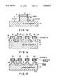
- FIGS. 1a through 1idiagrammatically illustrate the process by which the cathodes of the present invention are formed
- FIG. 2illustrates a silicon-tip field emission cathode array before the removal of the dielectric cap used in the formation thereof;
- FIG. 3is a diagrammatic perspective view of a silicon-tip field emission cathode array in partial cross-section
- FIGS. 4a and 4bprovide a diagrammatic illustration of apparatus for minimizing the gate electrode aperture
- FIGS. 5a-5eillustrate a modified form of the process of the invention.
- electron-emitting microcathodesare fabricated through the use of nanometer process technology to produce emitters having tips with very small radii and having gate electrodes spaced typically less than one micron from the tip apex.
- electron emitterscan be operated as cathodes in a field emission device at potentials of less than 100 volts.
- advantagecan be taken of the well characterized and understood conventional silicon processing techniques so that very large, densely packed arrays of silicon cathodes can be produced. As a result, large total currents and large current densities, as well as low operating voltages can be achieved.
- the present inventionis directed to a novel fabrication technique for the formation of silicon tip-type field emission cathodes having self-aligned gate electrodes and, if desired, self-aligned metal encapsulating films.
- the ability to provide self alignment of the gate electrode and the metal encapsulating filmpermits construction of field emission cathode tips on a nanometer scale with accuracy and reliability.
- the present inventioncontemplates, in one embodiment, the use of gold with a chrome adhesion layer for both the gate electrode and the encapsulating metal, in fact other metal films can be used. These films can be deposited using electron beam evaporation, thermal evaporation, or sputter deposition in the processes which is to be described below.
- Molybdenum and tungstenare ideal films where high temperature use is desired for the field emission cathodes or when removal of silicon oxides in vacuum using a thermal treatment is required. Accordingly, when the following description refers to "metal" in the fabrication process, it will be understood that the foregoing metals are preferred, although others may be used.
- the fabrication of self-aligned metal encapsulated silicon tip field emission cathode arraysstarts with a substrate which preferably is an n-type, (100) oriented, 10 18 arsenic doped silicon (5 m-ohm per cm), generally indicated at 10 in FIG. 1a, for example in the form of a wafer.
- the field emission tipsare formed from this material in the following manner.
- the top surface 12 of the substrateis cleaned and a silicon dioxide layer 14, illustrated as "Oxide I" is thermally grown on surface 12 to a thickness of, for example, 90 nm, at a temperature of 900° C.
- the oxide layer 14reduces the stress between the substrate 10 and a silicon nitride layer 16, identified in FIG.
- the nitride layer 16is applied to the top surface of the oxide layer 14 by low pressure chemical vapor deposition (LPCVD) to a thickness of about 400 nm and at a temperature of 850° C.
- LPCVDlow pressure chemical vapor deposition
- the locations and sizes of individual tip field emission cathodesare determined by lithography in a tri-layer resist material which is deposited on the nitride layer.
- the resist layermay include, for example, a polyimide base layer 18 which may be 800 nm thick, a plasma enhanced chemical vapor deposition (PECVD) interlayer oxide 20 having a thickness of 80 nm and a P(NMA-MAA) type I, 11% co-polymer top layer 22 having a thickness of 170 nm.
- PECVDplasma enhanced chemical vapor deposition
- P(NMA-MAA) type I11% co-polymer top layer 22 having a thickness of 170 nm.
- these circlesare located in an array of rows and columns to provide the desired pattern of field emission cathode tips.
- the copolymer layer 22is developed, and the inner layer oxide 20 is patterned using an isotropic reactive ion etch (RIE). Thereafter, the polyimide layer 18 is patterned using a high pressure oxygen (RIE) to thereby produce circular cavities such as the cavity 24 illustrated in FIG. 1b.
- RIEhigh pressure oxygen
- a 250 nm aluminum film 26is thermally evaporated onto the top surface of layer 22 and into the cavities 24, where it is deposited onto the top surface of the nitride layer 16 to thereby form circles of aluminum, such as the circle 28, on the nitride layer.
- Line of sight aluminum evaporationis used, and a pattern of circles 28 is produced on nitride layer 16 in accordance with the desired pattern of the array of field emission cathodes to be produced.
- the aluminum layer 26is removed by means of a methylene chloride lift off process which removes the resist sequence and the layer 26 of aluminum, leaving the aluminum circles 28 intact.
- the array pattern represented by the aluminum circles 28is then transferred to the underlying dielectric stack, consisting of nitride 16 and oxide 14, by means of an anisotropic RIE process, as illustrated in FIG. 1c.
- FIG. 1cillustrates only one aluminum circle and its dielectric stack, it will be understood that multiple circles may be provided on the top surface 12 of the substrate.
- a second anisotropic RIE processtransfers the pattern to the underlying substrate silicon by etching trenches, for example, 500 nm deep, into the substrate silicon.
- the bottom wall of the trenchis illustrated at 30 in FIG. 1d, and this trench extends between all of the dielectric stacks in the array to define upstanding cylindrical pedestals at the desired locations of the emitter.
- a conformal nitride layeris deposited by low pressure chemical vapor deposition to cover all of the exposed surfaces and then is etched back by an RIE etch to expose the trench surface 30 and to leave nitride side wall spacers 32 on the cylindrical side wall 34 of each of the upstanding silicon pillars 36.
- the side wall spacer nitride material 32which is illustrated in FIG. 1d as "Nitride II" is provided to prevent oxidation of the silicon pedestal 36 during the subsequent steps.
- the exposed surface 30 of the silicon substrate 10is further etched to a depth of 1 micrometer, for example, using an RIE recess etch, thereby forming recesses such as those illustrated at 40 in FIG. 1e.
- These recessesundercut the pedestal 36 (of FIG. 1d) below the nitride spacer 32 to form spaced, circular islands such as islands 46, 48, 50 and 52 supported above the remaining substrate 10.
- the islandsremain connected to the substrate 10 and are supported by corresponding silicon pillars 56, 58, 60 and 62, respectively.
- the islands and the corresponding pillarsconform in cross sectional shape to the aluminum deposition 28, and thus preferably are circular in cross section, with the pedestals 56, 58, 60 and 62 being tapered generally inwardly and upwardly.
- the apertures 40surround the pillars to provide a continuous surface 64 which surrounds the islands and the supporting pillars. As illustrated, the pillars have their smallest diameter at neck portion 66, where they join the bottom wall 68 of the corresponding
- FIG. 1eis then oxidized using high temperature lateral thermal oxidation (for example at a temperature of 1100° C.) to form a layer of oxide 70, illustrated in FIG. 1f, on the exposed surfaces of the silicon material 10.
- the thickness of layer 70is sufficient to oxidize all of the silicon in the region of the neck portion 66 of the pillars which support the silicon islands, and accordingly the thickness of the oxide layer will depend upon the diameter of the neck portion.
- an oxide thickness of approximately 600 nmwill be sufficient to remove all of the oxide in the area of the neck 66, silicon thereby separating the islands 46, 48, 50 and 52 from their corresponding supporting silicon pillars 56, 58, 60 and 62, and electrically isolating the islands from the underlying silicon substrate 10, as illustrated in FIG. 1f.
- the islands of substrate siliconare mechanically supported by the oxide layer and it has been found that the upper and lower silicon material will be defect free so long as the two parts are completely isolated by the lateral thermal oxidation which produces oxidation layer 70.
- Oxidation of the siliconmoves into the surface of the silicon material essentially at a constant rate, oxidizing the material inwardly at the neck 66 and the vertical side walls of the pillars, upwardly at the bottom surfaces 68 of the islands, and downwardly on the substrate surface 64, thereby reducing the size of the island 46 (for example) and reducing the diameter of the pillar 56 throughout its entire height.
- This oxidationshapes the bottom surface 68 of island 46 (as well as the other islands in the array) into a downwardly-facing tip 74 and shapes the pillar 56 into an upwardly-facing conical tip 76, with the tips 74 and 76 being opposed and aligned with each other.
- a gate electrode metal layer 80is deposited on the upper surfaces of the wafer as by line-of-sight evaporation to form a layer approximately 300 nm thick on the horizontal bottom surfaces 81 of apertures 40 surrounding the islands.
- the metalforms a layer 82 on the top and sides of the islands. Because of the presence of the oxide layer 70 on the surfaces of the upwardly-facing lower tips 76, and because the layer 70 is of uniform thickness, the metal layer 80 forms circular apertures around the conical tips 76 with the interior edges 86 of these apertures being spaced from the conical tips 76 by the thickness of the oxide layer.
- aperture 84is substantially the same as the diameter of its corresponding island 46, in the illustrated example, and preferably is about 1.8 micrometers.
- FIG. 2is a perspective and diagrammatic illustration of an array of the islands of FIG. 1g, showing the islands covered by the metal layer 82. As illustrated in this figure, the islands are supported by oxide pedestals formed by the oxide layer 70, with the gate electrode layer 80 covering the bottom of the openings 40 between the adjacent islands. The gate electrode layer 80 provides a continuous metal surface between the adjacent islands in all directions. Although the islands are shown in FIG. 2 as being arranged in rows along an X axis and columns along a Y axis, various other patterns and arrangements may be provided, as desired.
- the next step in the processis the removal of the islands 46, 48, etc. and the dielectric and metal caps which the islands support.
- the capsare lifted off by etching the wafer in a buffered hydrofluoric acid solution to remove the oxide layer 70 around the conical tips 76, as illustrated in FIG. 1h.
- the etching processis continued until the oxide layer 70 is removed from the side walls of the conical tips 76 to expose the tips, and until the metal layer 80 is undercut, as illustrated at 90.
- This undercuttingleaves an oxide support structure 92 beneath the gate electrode layer 80 to secure layer 80 to the floor 78 of the silicon substrate 10 and to hold it in position with respect to the tips 76.
- FIG. 3corresponds to FIG. 1h, showing the wafer with the islands 46, 48, etc. removed and the oxide layer removed from the tips 76.
- FIG. 3also shows the undercutting of the metal layer 80 adjacent the aperture 84 surrounding the tip 76 to leave support segments 92 of the oxide in place. This support structure 92 ensures that the apertures 84 remain accurately aligned with their corresponding tips.
- the circumferential edges 86 forming the apertures 84are tapered upwardly and inwardly to parallel the side wall of the corresponding tip 76 so that a constant gap 96 is formed between the gate electrode metal 80 and the adjacent field emission tip.
- the cathode emitter tipswere encapsulated with a 5 nm chrome adhesion film and 10 nm of gold.
- the gate aperture 84 formed in layer 80is approximately the same diameter as the cap formed by island 46 and its dielectric coatings, prior to the metallization step, as illustrated in FIG. 1f. If it is desired to reduce the diameter of this gate aperture, the metal layer 80 can be deposited by shadow evaporation, causing the metal 80 to be deposited on the sides of the pillars, thereby raising the level of &:he aperture 84 up the side wall of the oxide layer 70. Alternatively, this can be accomplished by depositing a thicker layer of the metal 80. However, the gap 96 is still determined by the thickness of layer 70.
- the minimum gap 96 between aperture 84 and the side wall of tip 76is a function of the diameter of the silicon neck portion 66, and thus of the thickness of the oxide required to form the opposing tips 74 and 76.
- the minimum diameter of the aperture 84is also a function of the diameter of the neck 66 and thus of the total thickness of the supporting neck after oxidation, but its actual diameter is dependent on its vertical location on the tapered tip.
- FIGS. 1, 2 and 3utilizes an essentially planar electrode layer 80, with the aperture 84 surrounding the tips 76 being in the same plane as the top surface of the electrode. However, it is often desirable to provide smaller apertures than are available with this planar arrangement. A method for doing this is illustrated in FIG. 4, to which reference is now made.
- FIG. 4illustrates apparatus for depositing the electrode metal onto the oxide layer of FIG. 1f by shadow evaporation, so as to increase the height of the tip which will be covered by the metal layer and to thereby reduce the diameter of the gate aperture.
- the substrate or wafer 10is secured to an inclined rotatable surface 110 when the step illustrated in FIG. 1f has been completed.
- the inclined surface 110is secured to a rotating chuck 112 so that the substrate can be rotated about an axis parallel to the direction of evaporation of the Metal I contained in a crucible 114, indicated by arrow 116, for deposition on the surface of the wafer.
- a rotating chuck 112so that the substrate can be rotated about an axis parallel to the direction of evaporation of the Metal I contained in a crucible 114, indicated by arrow 116, for deposition on the surface of the wafer.
- the evaporated metalis directed onto the surface of oxide 70 where it extends upwardly along the support pillar, with the shadow effect of the island 46 determining the height to which the metal is deposited. Since the pillar is tapered, the top edge of the metal, which defines the aperture 84, is reduced in diameter, and can be reduced to about 600 nm. This deposition results in a "dimple" 120 of metal around the tip, extending above the top surface 122 of the metal layer 80.
- FIGS. 5a-dAnother method for fabricating a dimpled gate electrode for the purpose of controlling the diameter of the gate aperture is illustrated diagrammatically in FIGS. 5a-d.
- FIG. 5ais an illustration of the island and pillar structure of FIG. 1e, and is fabricated in the manner described hereinabove.
- the structureincludes an island 46 supported by a pillar 56 on a substrate 10.
- the substrate 10, the aperture 40 between adjacent islands, and the horizontal surfaces of the substrate and the oxide and metal layers thereonare not illustrated in FIGS. 5b-5e.
- the dielectric capwhich includes the nitride spacer 32, as illustrated in FIG. 1d.
- This structureis oxidized, as in the prior embodiment of FIG. 1f, to produce the oxide layer 70 illustrated in FIG. 5b, to form upper and lower tips 74 and 76.
- the next step, shown in FIG. 5cincludes the deposition of a metal layer 130 on the oxide 70 by sputter deposition of TiW. The sputtered metal is also deposited on the dielectric cap carried by the island 46, as indicated at 132, but the nitride spacer 32 serves to break the TiW layer at the bottom surface of the island, as indicated at 134 in FIG. 5c.
- An aluminum mask 136is evaporated onto the surface of metal layer 130, as illustrated in FIG. 5d, with the upper edge 136 of the mask defining the location of the aperture to be formed in the metal layer 130.
- a layer 138 of aluminumalso covers the cap.
- the apertureis then formed by etching away the TiW near the top of the lower tip 76 with an SF 6 plasma etch; only the TiW not covered by aluminum is etched.
- the oxide exposed by removal of the TiW materialis etched by an HF wet chemical etch to lift off the island 46 and to expose the tip 76, leaving the dimple structure illustrated in FIG. 5e.
- This Figureshows two such tips, which may be part of a larger array, wherein the tips are surrounded by dimples of TiW forming the gate electrodes. These dimples are an extension of the overall electrode layer formed by the sputter deposition of TiW on the oxide layer.
- the dimpleseach form an aperture 140 having a diameter which is determined by the location of mask 134, and which is precisely aligned with the tip 76.
- the gap between the edge of aperture 140 and the tipis determined by the thickness of oxide layer 70, as before.
- the metal gate electrode layersuch as layer 80 in FIG. 3 may be patterned to divide the array into groups of emitters, or to separate single emitters, for control purposes.
- dividing grooves 150can be provided in the layer 80 by means of a gate electrode mask and a metal etching step.
- the surface of layer 80would be covered by, for example, an S1400-27 photoresist layer to a thickness of 1.2 ⁇ m, and the desired pattern exposed, through a suitable optical mask, as by light at 402 nm.
- An MF-312 photoresistdevelop is followed by a metal etching step to produce the groove 150 through the thickness of metal layer 80.
- the photoresist layeris removed, as by an acetone/IPA photoresist strip solution, leaving the patterned metal layer.
- Suitable electrical connectionsmay be made to the separate metal segments, such as segments 152 and 154, to provide suitable control voltages to corresponding emitter tips.
- the vertical placement of the tip with respect to the upper surface of the gate electrode 80can be varied by designing for different tip heights, as by lengthening the oxide step to reduce the size of tip 76.
- the process of the present inventionpermits fabrication of silicon tip micro-cathodes in arrays of very large numbers, with the tip to tip spacing between adjacent cathodes being in the range of 1.0 micrometers to, for example, 10 micrometers.
- the diameters of the tipsare uniform, and may be less than 20 nanometers, with the gate electrode being self-aligned with respect to the cathode tip.
- the position of the cathode with respect to the gate electrode aperturestrongly influences the emission characteristics, and accordingly the diameter of the aperture and its size and location with respect to the tip can be varied as desired.
- Cathodes with heights ranging from 500 nm to 900 nmhave been fabricated and structures have been produced with cathodes having their tips below, even with, and above the top surface of the gate metal layer 80.
- the process of the present inventionprovides uniform, self-aligned encapsulation of the tip by other metals, as explained with respect to FIG. 1i, without the need for an additional masking step and without the risk of substrate-to-gate electrode shorts.
Landscapes
- Engineering & Computer Science (AREA)
- Chemical & Material Sciences (AREA)
- Nanotechnology (AREA)
- Manufacturing & Machinery (AREA)
- Physics & Mathematics (AREA)
- Mathematical Physics (AREA)
- Theoretical Computer Science (AREA)
- Crystallography & Structural Chemistry (AREA)
- Cold Cathode And The Manufacture (AREA)
Abstract
Description
Claims (17)
Priority Applications (2)
| Application Number | Priority Date | Filing Date | Title |
|---|---|---|---|
| US07/803,986US5199917A (en) | 1991-12-09 | 1991-12-09 | Silicon tip field emission cathode arrays and fabrication thereof |
| US08/464,532US5627427A (en) | 1991-12-09 | 1995-06-05 | Silicon tip field emission cathodes |
Applications Claiming Priority (1)
| Application Number | Priority Date | Filing Date | Title |
|---|---|---|---|
| US07/803,986US5199917A (en) | 1991-12-09 | 1991-12-09 | Silicon tip field emission cathode arrays and fabrication thereof |
Related Child Applications (1)
| Application Number | Title | Priority Date | Filing Date |
|---|---|---|---|
| US851093ADivision | 1991-12-09 | 1993-01-25 |
Publications (1)
| Publication Number | Publication Date |
|---|---|
| US5199917Atrue US5199917A (en) | 1993-04-06 |
Family
ID=25187911
Family Applications (1)
| Application Number | Title | Priority Date | Filing Date |
|---|---|---|---|
| US07/803,986Expired - LifetimeUS5199917A (en) | 1991-12-09 | 1991-12-09 | Silicon tip field emission cathode arrays and fabrication thereof |
Country Status (1)
| Country | Link |
|---|---|
| US (1) | US5199917A (en) |
Cited By (72)
| Publication number | Priority date | Publication date | Assignee | Title |
|---|---|---|---|---|
| US5363021A (en)* | 1993-07-12 | 1994-11-08 | Cornell Research Foundation, Inc. | Massively parallel array cathode |
| US5374868A (en)* | 1992-09-11 | 1994-12-20 | Micron Display Technology, Inc. | Method for formation of a trench accessible cold-cathode field emission device |
| US5382185A (en)* | 1993-03-31 | 1995-01-17 | The United States Of America As Represented By The Secretary Of The Navy | Thin-film edge field emitter device and method of manufacture therefor |
| DE4421256A1 (en)* | 1993-06-17 | 1995-01-26 | Karlheinz Dipl Ing Bock | Field-effect microtriode |
| FR2709206A1 (en)* | 1993-06-14 | 1995-02-24 | Fujitsu Ltd | Cathode device having a small aperture and its method of manufacture |
| US5396150A (en)* | 1993-07-01 | 1995-03-07 | Industrial Technology Research Institute | Single tip redundancy method and resulting flat panel display |
| US5462467A (en)* | 1993-09-08 | 1995-10-31 | Silicon Video Corporation | Fabrication of filamentary field-emission device, including self-aligned gate |
| WO1996000975A1 (en)* | 1994-06-29 | 1996-01-11 | Candescent Technologies Corporation | Fabrication of electron-emitting structures using charged-particle tracks and removal of emitter material |
| WO1996002063A1 (en)* | 1994-07-12 | 1996-01-25 | Amoco Corporation | Volcano-shaped field emitter structures |
| US5503582A (en)* | 1994-11-18 | 1996-04-02 | Micron Display Technology, Inc. | Method for forming spacers for display devices employing reduced pressures |
| WO1996004674A3 (en)* | 1994-08-05 | 1996-05-02 | Central Research Lab Ltd | A self-aligned gate field emitter device and methods for producing the same |
| US5531880A (en)* | 1994-09-13 | 1996-07-02 | Microelectronics And Computer Technology Corporation | Method for producing thin, uniform powder phosphor for display screens |
| US5536988A (en)* | 1993-06-01 | 1996-07-16 | Cornell Research Foundation, Inc. | Compound stage MEM actuator suspended for multidimensional motion |
| US5536193A (en) | 1991-11-07 | 1996-07-16 | Microelectronics And Computer Technology Corporation | Method of making wide band gap field emitter |
| US5551903A (en) | 1992-03-16 | 1996-09-03 | Microelectronics And Computer Technology | Flat panel display based on diamond thin films |
| DE19509903A1 (en)* | 1995-03-18 | 1996-09-19 | Inst Mikrotechnik Mainz Gmbh | Prodn. of tip used in optical electron beam scanning microscope |
| US5559389A (en)* | 1993-09-08 | 1996-09-24 | Silicon Video Corporation | Electron-emitting devices having variously constituted electron-emissive elements, including cones or pedestals |
| EP0736891A1 (en)* | 1995-04-03 | 1996-10-09 | SHARP Corporation | Process of fabricating field-emission type electron source, electron source fabricated thereby and element structure of electron source |
| US5564959A (en)* | 1993-09-08 | 1996-10-15 | Silicon Video Corporation | Use of charged-particle tracks in fabricating gated electron-emitting devices |
| US5584740A (en)* | 1993-03-31 | 1996-12-17 | The United States Of America As Represented By The Secretary Of The Navy | Thin-film edge field emitter device and method of manufacture therefor |
| US5600200A (en) | 1992-03-16 | 1997-02-04 | Microelectronics And Computer Technology Corporation | Wire-mesh cathode |
| US5601966A (en) | 1993-11-04 | 1997-02-11 | Microelectronics And Computer Technology Corporation | Methods for fabricating flat panel display systems and components |
| US5612712A (en) | 1992-03-16 | 1997-03-18 | Microelectronics And Computer Technology Corporation | Diode structure flat panel display |
| US5620350A (en)* | 1994-10-27 | 1997-04-15 | Nec Corporation | Method for making a field-emission type electron gun |
| US5627427A (en)* | 1991-12-09 | 1997-05-06 | Cornell Research Foundation, Inc. | Silicon tip field emission cathodes |
| US5629583A (en)* | 1994-07-25 | 1997-05-13 | Fed Corporation | Flat panel display assembly comprising photoformed spacer structure, and method of making the same |
| US5628659A (en)* | 1995-04-24 | 1997-05-13 | Microelectronics And Computer Corporation | Method of making a field emission electron source with random micro-tip structures |
| US5637539A (en)* | 1996-01-16 | 1997-06-10 | Cornell Research Foundation, Inc. | Vacuum microelectronic devices with multiple planar electrodes |
| FR2744565A1 (en)* | 1996-02-07 | 1997-08-08 | Nec Corp | METHOD FOR MANUFACTURING A COLD FIELD EMISSION CATHODE |
| US5666020A (en)* | 1994-11-16 | 1997-09-09 | Nec Corporation | Field emission electron gun and method for fabricating the same |
| US5665618A (en)* | 1994-11-14 | 1997-09-09 | The United States Of America As Represented By The Secretary Of The Navy | Method of forming an interband lateral resonant tunneling transistor with single narrow gate electrode |
| US5675216A (en) | 1992-03-16 | 1997-10-07 | Microelectronics And Computer Technololgy Corp. | Amorphic diamond film flat field emission cathode |
| US5679043A (en) | 1992-03-16 | 1997-10-21 | Microelectronics And Computer Technology Corporation | Method of making a field emitter |
| US5763997A (en) | 1992-03-16 | 1998-06-09 | Si Diamond Technology, Inc. | Field emission display device |
| US5766446A (en)* | 1996-03-05 | 1998-06-16 | Candescent Technologies Corporation | Electrochemical removal of material, particularly excess emitter material in electron-emitting device |
| US5779514A (en)* | 1996-02-13 | 1998-07-14 | National Science Council | Technique to fabricate chimney-shaped emitters for field-emission devices |
| US5844251A (en)* | 1994-01-05 | 1998-12-01 | Cornell Research Foundation, Inc. | High aspect ratio probes with self-aligned control electrodes |
| WO1999003123A1 (en) | 1997-07-07 | 1999-01-21 | Candescent Technologies Corporation | Gate electrode formation method |
| US5866979A (en)* | 1994-09-16 | 1999-02-02 | Micron Technology, Inc. | Method for preventing junction leakage in field emission displays |
| US5893967A (en)* | 1996-03-05 | 1999-04-13 | Candescent Technologies Corporation | Impedance-assisted electrochemical removal of material, particularly excess emitter material in electron-emitting device |
| US5909033A (en)* | 1996-11-11 | 1999-06-01 | Matsushita Electric Industrial Co., Ltd. | Vacuum-sealed field-emission electron source and method of manufacturing the same |
| US5923948A (en)* | 1994-11-04 | 1999-07-13 | Micron Technology, Inc. | Method for sharpening emitter sites using low temperature oxidation processes |
| US5949182A (en)* | 1996-06-03 | 1999-09-07 | Cornell Research Foundation, Inc. | Light-emitting, nanometer scale, micromachined silicon tips |
| US5955849A (en)* | 1993-11-15 | 1999-09-21 | The United States Of America As Represented By The Secretary Of The Navy | Cold field emitters with thick focusing grids |
| US5975975A (en)* | 1994-09-16 | 1999-11-02 | Micron Technology, Inc. | Apparatus and method for stabilization of threshold voltage in field emission displays |
| US5986625A (en)* | 1997-01-07 | 1999-11-16 | Micron Technology, Inc. | Application specific field emission display including extended emitters |
| US6008062A (en)* | 1997-10-31 | 1999-12-28 | Candescent Technologies Corporation | Undercutting technique for creating coating in spaced-apart segments |
| US6010383A (en)* | 1997-10-31 | 2000-01-04 | Candescent Technologies Corporation | Protection of electron-emissive elements prior to removing excess emitter material during fabrication of electron-emitting device |
| US6022256A (en)* | 1996-11-06 | 2000-02-08 | Micron Display Technology, Inc. | Field emission display and method of making same |
| US6095883A (en)* | 1997-07-07 | 2000-08-01 | Candlescent Technologies Corporation | Spatially uniform deposition of polymer particles during gate electrode formation |
| US6120674A (en)* | 1997-06-30 | 2000-09-19 | Candescent Technologies Corporation | Electrochemical removal of material in electron-emitting device |
| US6127773A (en) | 1992-03-16 | 2000-10-03 | Si Diamond Technology, Inc. | Amorphic diamond film flat field emission cathode |
| US6204834B1 (en) | 1994-08-17 | 2001-03-20 | Si Diamond Technology, Inc. | System and method for achieving uniform screen brightness within a matrix display |
| US6296740B1 (en) | 1995-04-24 | 2001-10-02 | Si Diamond Technology, Inc. | Pretreatment process for a surface texturing process |
| US6417605B1 (en) | 1994-09-16 | 2002-07-09 | Micron Technology, Inc. | Method of preventing junction leakage in field emission devices |
| US20020136830A1 (en)* | 1999-09-01 | 2002-09-26 | Raina Kanwal K. | Method to increase the emission current in FED displays through the surface modification of the emitters |
| US20030057861A1 (en)* | 2000-01-14 | 2003-03-27 | Micron Technology, Inc. | Radiation shielding for field emitters |
| US20030155636A1 (en)* | 2002-02-15 | 2003-08-21 | Cobbley Chad A. | Molded stiffener for thin substrates |
| US20040067346A1 (en)* | 2000-12-19 | 2004-04-08 | Hofmann Wolfgang M. J. | Multiple-level actuators and clamping devices |
| US6797969B2 (en) | 2000-02-09 | 2004-09-28 | Fei Company | Multi-column FIB for nanofabrication applications |
| US20050180191A1 (en)* | 2001-10-11 | 2005-08-18 | Daniel Xu | Forming tapered lower electrode phase-change memories |
| US7025892B1 (en) | 1993-09-08 | 2006-04-11 | Candescent Technologies Corporation | Method for creating gated filament structures for field emission displays |
| US20120135571A1 (en)* | 2009-10-08 | 2012-05-31 | Chunghwa Picture Tubes, Ltd. | Manufacturing method of a thin film transistor |
| CN103641059A (en)* | 2013-12-30 | 2014-03-19 | 中国人民解放军国防科学技术大学 | Silicon-pillared metal film nano-structure array and preparation method thereof |
| US8778800B1 (en)* | 2011-03-23 | 2014-07-15 | Hrl Laboratories, Llc | Methods of making supercapacitor cells and micro-supercapacitors |
| US9053890B2 (en) | 2013-08-02 | 2015-06-09 | University Health Network | Nanostructure field emission cathode structure and method for making |
| US9196447B2 (en) | 2012-12-04 | 2015-11-24 | Massachusetts Institutes Of Technology | Self-aligned gated emitter tip arrays |
| US9748071B2 (en) | 2013-02-05 | 2017-08-29 | Massachusetts Institute Of Technology | Individually switched field emission arrays |
| US9934933B1 (en)* | 2017-01-19 | 2018-04-03 | Kla-Tencor Corporation | Extractor electrode for electron source |
| US10832885B2 (en) | 2015-12-23 | 2020-11-10 | Massachusetts Institute Of Technology | Electron transparent membrane for cold cathode devices |
| US10943760B2 (en) | 2018-10-12 | 2021-03-09 | Kla Corporation | Electron gun and electron microscope |
| US11719652B2 (en) | 2020-02-04 | 2023-08-08 | Kla Corporation | Semiconductor metrology and inspection based on an x-ray source with an electron emitter array |
Citations (14)
| Publication number | Priority date | Publication date | Assignee | Title |
|---|---|---|---|---|
| US3453478A (en)* | 1966-05-31 | 1969-07-01 | Stanford Research Inst | Needle-type electron source |
| US3755704A (en)* | 1970-02-06 | 1973-08-28 | Stanford Research Inst | Field emission cathode structures and devices utilizing such structures |
| US3789471A (en)* | 1970-02-06 | 1974-02-05 | Stanford Research Inst | Field emission cathode structures, devices utilizing such structures, and methods of producing such structures |
| US3814968A (en)* | 1972-02-11 | 1974-06-04 | Lucas Industries Ltd | Solid state radiation sensitive field electron emitter and methods of fabrication thereof |
| US3921022A (en)* | 1974-09-03 | 1975-11-18 | Rca Corp | Field emitting device and method of making same |
| US3970887A (en)* | 1974-06-19 | 1976-07-20 | Micro-Bit Corporation | Micro-structure field emission electron source |
| US4095133A (en)* | 1976-04-29 | 1978-06-13 | U.S. Philips Corporation | Field emission device |
| US4178531A (en)* | 1977-06-15 | 1979-12-11 | Rca Corporation | CRT with field-emission cathode |
| US4575765A (en)* | 1982-11-25 | 1986-03-11 | Man Maschinenfabrik Augsburg Nurnberg Ag | Method and apparatus for transmitting images to a viewing screen |
| US4721885A (en)* | 1987-02-11 | 1988-01-26 | Sri International | Very high speed integrated microelectronic tubes |
| US4940916A (en)* | 1987-11-06 | 1990-07-10 | Commissariat A L'energie Atomique | Electron source with micropoint emissive cathodes and display means by cathodoluminescence excited by field emission using said source |
| US4943343A (en)* | 1989-08-14 | 1990-07-24 | Zaher Bardai | Self-aligned gate process for fabricating field emitter arrays |
| US4964946A (en)* | 1990-02-02 | 1990-10-23 | The United States Of America As Represented By The Secretary Of The Navy | Process for fabricating self-aligned field emitter arrays |
| US4983878A (en)* | 1987-09-04 | 1991-01-08 | The General Electric Company, P.L.C. | Field induced emission devices and method of forming same |
- 1991
- 1991-12-09USUS07/803,986patent/US5199917A/ennot_activeExpired - Lifetime
Patent Citations (15)
| Publication number | Priority date | Publication date | Assignee | Title |
|---|---|---|---|---|
| US3453478A (en)* | 1966-05-31 | 1969-07-01 | Stanford Research Inst | Needle-type electron source |
| US3755704A (en)* | 1970-02-06 | 1973-08-28 | Stanford Research Inst | Field emission cathode structures and devices utilizing such structures |
| US3789471A (en)* | 1970-02-06 | 1974-02-05 | Stanford Research Inst | Field emission cathode structures, devices utilizing such structures, and methods of producing such structures |
| US3814968A (en)* | 1972-02-11 | 1974-06-04 | Lucas Industries Ltd | Solid state radiation sensitive field electron emitter and methods of fabrication thereof |
| US3970887A (en)* | 1974-06-19 | 1976-07-20 | Micro-Bit Corporation | Micro-structure field emission electron source |
| US3921022A (en)* | 1974-09-03 | 1975-11-18 | Rca Corp | Field emitting device and method of making same |
| US4095133A (en)* | 1976-04-29 | 1978-06-13 | U.S. Philips Corporation | Field emission device |
| US4178531A (en)* | 1977-06-15 | 1979-12-11 | Rca Corporation | CRT with field-emission cathode |
| US4575765A (en)* | 1982-11-25 | 1986-03-11 | Man Maschinenfabrik Augsburg Nurnberg Ag | Method and apparatus for transmitting images to a viewing screen |
| US4721885A (en)* | 1987-02-11 | 1988-01-26 | Sri International | Very high speed integrated microelectronic tubes |
| US4983878A (en)* | 1987-09-04 | 1991-01-08 | The General Electric Company, P.L.C. | Field induced emission devices and method of forming same |
| US4940916A (en)* | 1987-11-06 | 1990-07-10 | Commissariat A L'energie Atomique | Electron source with micropoint emissive cathodes and display means by cathodoluminescence excited by field emission using said source |
| US4940916B1 (en)* | 1987-11-06 | 1996-11-26 | Commissariat Energie Atomique | Electron source with micropoint emissive cathodes and display means by cathodoluminescence excited by field emission using said source |
| US4943343A (en)* | 1989-08-14 | 1990-07-24 | Zaher Bardai | Self-aligned gate process for fabricating field emitter arrays |
| US4964946A (en)* | 1990-02-02 | 1990-10-23 | The United States Of America As Represented By The Secretary Of The Navy | Process for fabricating self-aligned field emitter arrays |
Non-Patent Citations (12)
| Title |
|---|
| "A Fully Depleted Lean-Channel Transistor (DELTA) A Novel Vertical Ultrathin SOI MOSFET" Hisamoto; Manuscript received Sep. 6, 1989; Central Research Laboratory, Hitachi Ltd. IEEE Log Number 8933301, 1990 IEEE. |
| "Field Emitter Tips for Vacuum Microelectronic Devices" Chin; J. Vac. Sci. Technol. A 8 (4) Jul./Aug. 1990 pp. 3586-3590. |
| "Formation of Submicron Silicon-on Insulator Structures by Lateral Oxidation of Substrate-Silicon Islands" Arney et al. J. Vac. Sci. Technol. B 6 (1) Jan./Feb. 1988 1988 American Vacuum Society pp. 341-345. |
| "Self-Aligned Silicon-Strip Field Emitter Array" Spallas et al.; Inst. Phys. Conf. Ser. No. 99: Section 1 Paper presented at 2nd Int. Conf. on Vac. Microelectron, Bath, 1989, pp. 1-4. |
| "TEM Characterization of Defect Configurations in Submicron SOI Structures", Theodore et al.; Preprint: Proc. 6th Int. Conf. on Microscopy of Semiconducting Materials Oxford, UK 10-13 Apr. 1989 pp. 551-556. |
| "Triode Operation of a Vacuum Tansistor", Busta et al. IEDM 91-213-215. |
| A Fully Depleted Lean Channel Transistor (DELTA) A Novel Vertical Ultrathin SOI MOSFET Hisamoto; Manuscript received Sep. 6, 1989; Central Research Laboratory, Hitachi Ltd. IEEE Log Number 8933301, 1990 IEEE.* |
| Field Emitter Tips for Vacuum Microelectronic Devices Chin; J. Vac. Sci. Technol. A 8 (4) Jul./Aug. 1990 pp. 3586 3590.* |
| Formation of Submicron Silicon on Insulator Structures by Lateral Oxidation of Substrate Silicon Islands Arney et al. J. Vac. Sci. Technol. B 6 (1) Jan./Feb. 1988 1988 American Vacuum Society pp. 341 345.* |
| Self Aligned Silicon Strip Field Emitter Array Spallas et al.; Inst. Phys. Conf. Ser. No. 99: Section 1 Paper presented at 2nd Int. Conf. on Vac. Microelectron, Bath, 1989, pp. 1 4.* |
| TEM Characterization of Defect Configurations in Submicron SOI Structures , Theodore et al.; Preprint: Proc. 6th Int. Conf. on Microscopy of Semiconducting Materials Oxford, UK 10 13 Apr. 1989 pp. 551 556.* |
| Triode Operation of a Vacuum Tansistor , Busta et al. IEDM 91 213 215.* |
Cited By (120)
| Publication number | Priority date | Publication date | Assignee | Title |
|---|---|---|---|---|
| US5536193A (en) | 1991-11-07 | 1996-07-16 | Microelectronics And Computer Technology Corporation | Method of making wide band gap field emitter |
| US5861707A (en) | 1991-11-07 | 1999-01-19 | Si Diamond Technology, Inc. | Field emitter with wide band gap emission areas and method of using |
| US5627427A (en)* | 1991-12-09 | 1997-05-06 | Cornell Research Foundation, Inc. | Silicon tip field emission cathodes |
| US5686791A (en) | 1992-03-16 | 1997-11-11 | Microelectronics And Computer Technology Corp. | Amorphic diamond film flat field emission cathode |
| US5551903A (en) | 1992-03-16 | 1996-09-03 | Microelectronics And Computer Technology | Flat panel display based on diamond thin films |
| US5600200A (en) | 1992-03-16 | 1997-02-04 | Microelectronics And Computer Technology Corporation | Wire-mesh cathode |
| US6127773A (en) | 1992-03-16 | 2000-10-03 | Si Diamond Technology, Inc. | Amorphic diamond film flat field emission cathode |
| US6629869B1 (en) | 1992-03-16 | 2003-10-07 | Si Diamond Technology, Inc. | Method of making flat panel displays having diamond thin film cathode |
| US5675216A (en) | 1992-03-16 | 1997-10-07 | Microelectronics And Computer Technololgy Corp. | Amorphic diamond film flat field emission cathode |
| US5763997A (en) | 1992-03-16 | 1998-06-09 | Si Diamond Technology, Inc. | Field emission display device |
| US5703435A (en) | 1992-03-16 | 1997-12-30 | Microelectronics & Computer Technology Corp. | Diamond film flat field emission cathode |
| US5679043A (en) | 1992-03-16 | 1997-10-21 | Microelectronics And Computer Technology Corporation | Method of making a field emitter |
| US5612712A (en) | 1992-03-16 | 1997-03-18 | Microelectronics And Computer Technology Corporation | Diode structure flat panel display |
| US5374868A (en)* | 1992-09-11 | 1994-12-20 | Micron Display Technology, Inc. | Method for formation of a trench accessible cold-cathode field emission device |
| US5382185A (en)* | 1993-03-31 | 1995-01-17 | The United States Of America As Represented By The Secretary Of The Navy | Thin-film edge field emitter device and method of manufacture therefor |
| US5584740A (en)* | 1993-03-31 | 1996-12-17 | The United States Of America As Represented By The Secretary Of The Navy | Thin-film edge field emitter device and method of manufacture therefor |
| US5536988A (en)* | 1993-06-01 | 1996-07-16 | Cornell Research Foundation, Inc. | Compound stage MEM actuator suspended for multidimensional motion |
| US5775968A (en)* | 1993-06-14 | 1998-07-07 | Fujitsu Limited | Cathode device having smaller opening |
| US5576594A (en)* | 1993-06-14 | 1996-11-19 | Fujitsu Limited | Cathode device having smaller opening |
| US6140760A (en)* | 1993-06-14 | 2000-10-31 | Fujitsu Limited | Cathode device having smaller opening |
| FR2709206A1 (en)* | 1993-06-14 | 1995-02-24 | Fujitsu Ltd | Cathode device having a small aperture and its method of manufacture |
| DE4421256A1 (en)* | 1993-06-17 | 1995-01-26 | Karlheinz Dipl Ing Bock | Field-effect microtriode |
| DE4421256C2 (en)* | 1993-06-17 | 1998-10-01 | Karlheinz Dipl Ing Bock | Field effect microtriode array |
| US5396150A (en)* | 1993-07-01 | 1995-03-07 | Industrial Technology Research Institute | Single tip redundancy method and resulting flat panel display |
| US5363021A (en)* | 1993-07-12 | 1994-11-08 | Cornell Research Foundation, Inc. | Massively parallel array cathode |
| US5559389A (en)* | 1993-09-08 | 1996-09-24 | Silicon Video Corporation | Electron-emitting devices having variously constituted electron-emissive elements, including cones or pedestals |
| US5578185A (en)* | 1993-09-08 | 1996-11-26 | Silicon Video Corporation | Method for creating gated filament structures for field emision displays |
| US5801477A (en)* | 1993-09-08 | 1998-09-01 | Candescent Technologies Corporation | Gated filament structures for a field emission display |
| US5913704A (en)* | 1993-09-08 | 1999-06-22 | Candescent Technologies Corporation | Fabrication of electronic devices by method that involves ion tracking |
| US7025892B1 (en) | 1993-09-08 | 2006-04-11 | Candescent Technologies Corporation | Method for creating gated filament structures for field emission displays |
| US5462467A (en)* | 1993-09-08 | 1995-10-31 | Silicon Video Corporation | Fabrication of filamentary field-emission device, including self-aligned gate |
| US6204596B1 (en)* | 1993-09-08 | 2001-03-20 | Candescent Technologies Corporation | Filamentary electron-emission device having self-aligned gate or/and lower conductive/resistive region |
| US5827099A (en)* | 1993-09-08 | 1998-10-27 | Candescent Technologies Corporation | Use of early formed lift-off layer in fabricating gated electron-emitting devices |
| US5562516A (en)* | 1993-09-08 | 1996-10-08 | Silicon Video Corporation | Field-emitter fabrication using charged-particle tracks |
| US6515407B1 (en) | 1993-09-08 | 2003-02-04 | Candescent Technologies Corporation | Gated filament structures for a field emission display |
| US5564959A (en)* | 1993-09-08 | 1996-10-15 | Silicon Video Corporation | Use of charged-particle tracks in fabricating gated electron-emitting devices |
| US5851669A (en)* | 1993-09-08 | 1998-12-22 | Candescent Technologies Corporation | Field-emission device that utilizes filamentary electron-emissive elements and typically has self-aligned gate |
| US5813892A (en)* | 1993-09-08 | 1998-09-29 | Candescent Technologies Corporation | Use of charged-particle tracks in fabricating electron-emitting device having resistive layer |
| US5652083A (en) | 1993-11-04 | 1997-07-29 | Microelectronics And Computer Technology Corporation | Methods for fabricating flat panel display systems and components |
| US5614353A (en) | 1993-11-04 | 1997-03-25 | Si Diamond Technology, Inc. | Methods for fabricating flat panel display systems and components |
| US5601966A (en) | 1993-11-04 | 1997-02-11 | Microelectronics And Computer Technology Corporation | Methods for fabricating flat panel display systems and components |
| US5955849A (en)* | 1993-11-15 | 1999-09-21 | The United States Of America As Represented By The Secretary Of The Navy | Cold field emitters with thick focusing grids |
| US6027951A (en)* | 1994-01-05 | 2000-02-22 | Macdonald; Noel C. | Method of making high aspect ratio probes with self-aligned control electrodes |
| US5844251A (en)* | 1994-01-05 | 1998-12-01 | Cornell Research Foundation, Inc. | High aspect ratio probes with self-aligned control electrodes |
| US5607335A (en)* | 1994-06-29 | 1997-03-04 | Silicon Video Corporation | Fabrication of electron-emitting structures using charged-particle tracks and removal of emitter material |
| WO1996000975A1 (en)* | 1994-06-29 | 1996-01-11 | Candescent Technologies Corporation | Fabrication of electron-emitting structures using charged-particle tracks and removal of emitter material |
| WO1996002063A1 (en)* | 1994-07-12 | 1996-01-25 | Amoco Corporation | Volcano-shaped field emitter structures |
| US5629583A (en)* | 1994-07-25 | 1997-05-13 | Fed Corporation | Flat panel display assembly comprising photoformed spacer structure, and method of making the same |
| WO1996004674A3 (en)* | 1994-08-05 | 1996-05-02 | Central Research Lab Ltd | A self-aligned gate field emitter device and methods for producing the same |
| US5818153A (en)* | 1994-08-05 | 1998-10-06 | Central Research Laboratories Limited | Self-aligned gate field emitter device and methods for producing the same |
| US6204834B1 (en) | 1994-08-17 | 2001-03-20 | Si Diamond Technology, Inc. | System and method for achieving uniform screen brightness within a matrix display |
| US5531880A (en)* | 1994-09-13 | 1996-07-02 | Microelectronics And Computer Technology Corporation | Method for producing thin, uniform powder phosphor for display screens |
| US6712664B2 (en) | 1994-09-16 | 2004-03-30 | Micron Technology, Inc. | Process of preventing junction leakage in field emission devices |
| US6987352B2 (en) | 1994-09-16 | 2006-01-17 | Micron Technology, Inc. | Method of preventing junction leakage in field emission devices |
| US7629736B2 (en) | 1994-09-16 | 2009-12-08 | Micron Technology, Inc. | Method and device for preventing junction leakage in field emission devices |
| US7268482B2 (en) | 1994-09-16 | 2007-09-11 | Micron Technology, Inc. | Preventing junction leakage in field emission devices |
| US5866979A (en)* | 1994-09-16 | 1999-02-02 | Micron Technology, Inc. | Method for preventing junction leakage in field emission displays |
| US20060226761A1 (en)* | 1994-09-16 | 2006-10-12 | Hofmann James J | Method of preventing junction leakage in field emission devices |
| US7098587B2 (en) | 1994-09-16 | 2006-08-29 | Micron Technology, Inc. | Preventing junction leakage in field emission devices |
| US20060186790A1 (en)* | 1994-09-16 | 2006-08-24 | Hofmann James J | Method of preventing junction leakage in field emission devices |
| US6020683A (en)* | 1994-09-16 | 2000-02-01 | Micron Technology, Inc. | Method of preventing junction leakage in field emission displays |
| US6186850B1 (en) | 1994-09-16 | 2001-02-13 | Micron Technology, Inc. | Method of preventing junction leakage in field emission displays |
| US6676471B2 (en) | 1994-09-16 | 2004-01-13 | Micron Technology, Inc. | Method of preventing junction leakage in field emission displays |
| US20030184213A1 (en)* | 1994-09-16 | 2003-10-02 | Hofmann James J. | Method of preventing junction leakage in field emission devices |
| US5975975A (en)* | 1994-09-16 | 1999-11-02 | Micron Technology, Inc. | Apparatus and method for stabilization of threshold voltage in field emission displays |
| US6398608B1 (en) | 1994-09-16 | 2002-06-04 | Micron Technology, Inc. | Method of preventing junction leakage in field emission displays |
| US6417605B1 (en) | 1994-09-16 | 2002-07-09 | Micron Technology, Inc. | Method of preventing junction leakage in field emission devices |
| US5620350A (en)* | 1994-10-27 | 1997-04-15 | Nec Corporation | Method for making a field-emission type electron gun |
| US5923948A (en)* | 1994-11-04 | 1999-07-13 | Micron Technology, Inc. | Method for sharpening emitter sites using low temperature oxidation processes |
| US6312965B1 (en) | 1994-11-04 | 2001-11-06 | Micron Technology, Inc. | Method for sharpening emitter sites using low temperature oxidation process |
| US5665618A (en)* | 1994-11-14 | 1997-09-09 | The United States Of America As Represented By The Secretary Of The Navy | Method of forming an interband lateral resonant tunneling transistor with single narrow gate electrode |
| US5804475A (en)* | 1994-11-14 | 1998-09-08 | The United States Of America As Represented By The Secretary Of The Navy | Method of forming an interband lateral resonant tunneling transistor |
| US5666020A (en)* | 1994-11-16 | 1997-09-09 | Nec Corporation | Field emission electron gun and method for fabricating the same |
| US5503582A (en)* | 1994-11-18 | 1996-04-02 | Micron Display Technology, Inc. | Method for forming spacers for display devices employing reduced pressures |
| DE19509903A1 (en)* | 1995-03-18 | 1996-09-19 | Inst Mikrotechnik Mainz Gmbh | Prodn. of tip used in optical electron beam scanning microscope |
| US5800233A (en)* | 1995-04-03 | 1998-09-01 | Sharp Kabushiki Kaisha | Process of fabricating field-emission type electron source, electron source fabricated thereby and element structure of electron source |
| EP0736891A1 (en)* | 1995-04-03 | 1996-10-09 | SHARP Corporation | Process of fabricating field-emission type electron source, electron source fabricated thereby and element structure of electron source |
| US5628659A (en)* | 1995-04-24 | 1997-05-13 | Microelectronics And Computer Corporation | Method of making a field emission electron source with random micro-tip structures |
| US6296740B1 (en) | 1995-04-24 | 2001-10-02 | Si Diamond Technology, Inc. | Pretreatment process for a surface texturing process |
| US5637539A (en)* | 1996-01-16 | 1997-06-10 | Cornell Research Foundation, Inc. | Vacuum microelectronic devices with multiple planar electrodes |
| FR2744565A1 (en)* | 1996-02-07 | 1997-08-08 | Nec Corp | METHOD FOR MANUFACTURING A COLD FIELD EMISSION CATHODE |
| US5924903A (en)* | 1996-02-07 | 1999-07-20 | Nec Corporation | Method of fabricating a cold cathode for field emission |
| US5779514A (en)* | 1996-02-13 | 1998-07-14 | National Science Council | Technique to fabricate chimney-shaped emitters for field-emission devices |
| US5766446A (en)* | 1996-03-05 | 1998-06-16 | Candescent Technologies Corporation | Electrochemical removal of material, particularly excess emitter material in electron-emitting device |
| US5893967A (en)* | 1996-03-05 | 1999-04-13 | Candescent Technologies Corporation | Impedance-assisted electrochemical removal of material, particularly excess emitter material in electron-emitting device |
| US5949182A (en)* | 1996-06-03 | 1999-09-07 | Cornell Research Foundation, Inc. | Light-emitting, nanometer scale, micromachined silicon tips |
| US6022256A (en)* | 1996-11-06 | 2000-02-08 | Micron Display Technology, Inc. | Field emission display and method of making same |
| US5909033A (en)* | 1996-11-11 | 1999-06-01 | Matsushita Electric Industrial Co., Ltd. | Vacuum-sealed field-emission electron source and method of manufacturing the same |
| KR100485917B1 (en)* | 1996-11-11 | 2005-09-02 | 마츠시타 덴끼 산교 가부시키가이샤 | Vacuum sealed field emission type electron source device and its manufacturing method |
| US5986625A (en)* | 1997-01-07 | 1999-11-16 | Micron Technology, Inc. | Application specific field emission display including extended emitters |
| US6120674A (en)* | 1997-06-30 | 2000-09-19 | Candescent Technologies Corporation | Electrochemical removal of material in electron-emitting device |
| US6039621A (en)* | 1997-07-07 | 2000-03-21 | Candescent Technologies Corporation | Gate electrode formation method |
| WO1999003123A1 (en) | 1997-07-07 | 1999-01-21 | Candescent Technologies Corporation | Gate electrode formation method |
| US6095883A (en)* | 1997-07-07 | 2000-08-01 | Candlescent Technologies Corporation | Spatially uniform deposition of polymer particles during gate electrode formation |
| US6008062A (en)* | 1997-10-31 | 1999-12-28 | Candescent Technologies Corporation | Undercutting technique for creating coating in spaced-apart segments |
| US6010383A (en)* | 1997-10-31 | 2000-01-04 | Candescent Technologies Corporation | Protection of electron-emissive elements prior to removing excess emitter material during fabrication of electron-emitting device |
| US20020136830A1 (en)* | 1999-09-01 | 2002-09-26 | Raina Kanwal K. | Method to increase the emission current in FED displays through the surface modification of the emitters |
| US7101586B2 (en)* | 1999-09-01 | 2006-09-05 | Micron Technology, Inc. | Method to increase the emission current in FED displays through the surface modification of the emitters |
| US6860777B2 (en) | 2000-01-14 | 2005-03-01 | Micron Technology, Inc. | Radiation shielding for field emitters |
| US20030057861A1 (en)* | 2000-01-14 | 2003-03-27 | Micron Technology, Inc. | Radiation shielding for field emitters |
| US6797969B2 (en) | 2000-02-09 | 2004-09-28 | Fei Company | Multi-column FIB for nanofabrication applications |
| US6767614B1 (en) | 2000-12-19 | 2004-07-27 | Wolfgang M. J. Hofmann | Multiple-level actuators and clamping devices |
| US20040067346A1 (en)* | 2000-12-19 | 2004-04-08 | Hofmann Wolfgang M. J. | Multiple-level actuators and clamping devices |
| US20050180191A1 (en)* | 2001-10-11 | 2005-08-18 | Daniel Xu | Forming tapered lower electrode phase-change memories |
| US7422917B2 (en)* | 2001-10-11 | 2008-09-09 | Ovonyx, Inc. | Forming tapered lower electrode phase-change memories |
| US20030155636A1 (en)* | 2002-02-15 | 2003-08-21 | Cobbley Chad A. | Molded stiffener for thin substrates |
| US8148803B2 (en)* | 2002-02-15 | 2012-04-03 | Micron Technology, Inc. | Molded stiffener for thin substrates |
| US8716849B2 (en) | 2002-02-15 | 2014-05-06 | Micron Technology, Inc. | Semiconductor device including one or more stiffening elements |
| US20120135571A1 (en)* | 2009-10-08 | 2012-05-31 | Chunghwa Picture Tubes, Ltd. | Manufacturing method of a thin film transistor |
| US8247277B2 (en)* | 2009-10-08 | 2012-08-21 | Chunghwa Picture Tubes, Ltd. | Manufacturing method of a thin film transistor |
| US8778800B1 (en)* | 2011-03-23 | 2014-07-15 | Hrl Laboratories, Llc | Methods of making supercapacitor cells and micro-supercapacitors |
| US9196447B2 (en) | 2012-12-04 | 2015-11-24 | Massachusetts Institutes Of Technology | Self-aligned gated emitter tip arrays |
| US9748071B2 (en) | 2013-02-05 | 2017-08-29 | Massachusetts Institute Of Technology | Individually switched field emission arrays |
| US9053890B2 (en) | 2013-08-02 | 2015-06-09 | University Health Network | Nanostructure field emission cathode structure and method for making |
| CN103641059B (en)* | 2013-12-30 | 2016-03-30 | 中国人民解放军国防科学技术大学 | Metal film nano-structure array that silicon post supports and preparation method thereof |
| CN103641059A (en)* | 2013-12-30 | 2014-03-19 | 中国人民解放军国防科学技术大学 | Silicon-pillared metal film nano-structure array and preparation method thereof |
| US10832885B2 (en) | 2015-12-23 | 2020-11-10 | Massachusetts Institute Of Technology | Electron transparent membrane for cold cathode devices |
| US9934933B1 (en)* | 2017-01-19 | 2018-04-03 | Kla-Tencor Corporation | Extractor electrode for electron source |
| US10943760B2 (en) | 2018-10-12 | 2021-03-09 | Kla Corporation | Electron gun and electron microscope |
| US11719652B2 (en) | 2020-02-04 | 2023-08-08 | Kla Corporation | Semiconductor metrology and inspection based on an x-ray source with an electron emitter array |
Similar Documents
| Publication | Publication Date | Title |
|---|---|---|
| US5199917A (en) | Silicon tip field emission cathode arrays and fabrication thereof | |
| US5627427A (en) | Silicon tip field emission cathodes | |
| CA2034481C (en) | Self-aligned gate process for fabricating field emitter arrays | |
| US5266530A (en) | Self-aligned gated electron field emitter | |
| US5637539A (en) | Vacuum microelectronic devices with multiple planar electrodes | |
| US5493173A (en) | Field emission cold cathode and method for manufacturing the same | |
| US5543686A (en) | Electrostatic focussing means for field emission displays | |
| JPH06267403A (en) | Field emission type cold cathode and manufacture thereof | |
| US5502314A (en) | Field-emission element having a cathode with a small radius | |
| US5844351A (en) | Field emitter device, and veil process for THR fabrication thereof | |
| KR100274402B1 (en) | Method of fabricating a field emmission cold cathode | |
| US6246069B1 (en) | Thin-film edge field emitter device | |
| EP0841678B1 (en) | Vacuum-sealed field-emission electron source and method of manufacturing the same | |
| JP2809078B2 (en) | Field emission cold cathode and method of manufacturing the same | |
| JPH09259740A (en) | Vacuum micro-device and manufacture thereof | |
| US7140942B2 (en) | Gated electron emitter having supported gate | |
| US5607335A (en) | Fabrication of electron-emitting structures using charged-particle tracks and removal of emitter material | |
| US5930590A (en) | Fabrication of volcano-shaped field emitters by chemical-mechanical polishing (CMP) | |
| KR0174126B1 (en) | Method for making a field emission type electron gun | |
| JP2007518223A (en) | Hybrid multi-beam electron emission device with divergence control function | |
| EP0569671A1 (en) | Field emission cold cathode and method for manufacturing the same | |
| JPH06111712A (en) | Field emission cathode and manufacturing method thereof | |
| JP3223650B2 (en) | Field emission cathode | |
| KR100586740B1 (en) | Electron Beam Micro Source, Electron Beam Microcolumn Module Using Carbon Nanotube Tip and Manufacturing Method Thereof | |
| US6027632A (en) | Multi-step removal of excess emitter material in fabricating electron-emitting device |
Legal Events
| Date | Code | Title | Description |
|---|---|---|---|
| AS | Assignment | Owner name:CORNELL RESEARCH FOUNDATION, INC. A CORP. OF NEW Free format text:ASSIGNMENT OF ASSIGNORS INTEREST.;ASSIGNOR:MACDONALD, NOEL C.;REEL/FRAME:006004/0448 Effective date:19911209 | |
| AS | Assignment | Owner name:CORNELL RESEARCH FOUNDATION, INC., NEW YORK Free format text:ASSIGNMENT OF ASSIGNORS INTEREST.;ASSIGNORS:MACDONALD, NOEL C.;SPALLAS, JAMES P.;REEL/FRAME:006006/0082;SIGNING DATES FROM 19920116 TO 19920120 | |
| STCF | Information on status: patent grant | Free format text:PATENTED CASE | |
| CC | Certificate of correction | ||
| FEPP | Fee payment procedure | Free format text:PAYOR NUMBER ASSIGNED (ORIGINAL EVENT CODE: ASPN); ENTITY STATUS OF PATENT OWNER: SMALL ENTITY | |
| FPAY | Fee payment | Year of fee payment:4 | |
| FPAY | Fee payment | Year of fee payment:8 | |
| AS | Assignment | Owner name:VENTURE LENDING & LEASING III, INC., AS AGENT, CAL Free format text:SECURITY AGREEMENT;ASSIGNOR:CALIENT OPTICAL COMPONENTS, INC.;REEL/FRAME:011934/0464 Effective date:20010516 | |
| AS | Assignment | Owner name:PENTECH FINANCIAL SERVICES, INC., CALIFORNIA Free format text:SECURITY INTEREST;ASSIGNOR:CALIENT OPTICAL COMPONENTS, INC.;REEL/FRAME:012252/0175 Effective date:20010516 | |
| FPAY | Fee payment | Year of fee payment:12 | |
| AS | Assignment | Owner name:CALIENT OPTICAL COMPONENTS, INC., NEW YORK Free format text:RELEASE AGREEMENT;ASSIGNORS:VENTURE LENDING;LEASING III, INC.;REEL/FRAME:016172/0341 Effective date:20040825 Owner name:CALIENT OPTICAL COMPONENTS, INC., NEW YORK Free format text:RELEASE AGREEMENT;ASSIGNOR:PENTECH FINANCIAL SERVICES, INC.;REEL/FRAME:016182/0031 Effective date:20040831 | |
| FEPP | Fee payment procedure | Free format text:PAYER NUMBER DE-ASSIGNED (ORIGINAL EVENT CODE: RMPN); ENTITY STATUS OF PATENT OWNER: SMALL ENTITY Free format text:PAYOR NUMBER ASSIGNED (ORIGINAL EVENT CODE: ASPN); ENTITY STATUS OF PATENT OWNER: SMALL ENTITY |