US5199049A - Circuit and method of digital carrier detection for burst mode communication systems - Google Patents
Circuit and method of digital carrier detection for burst mode communication systemsDownload PDFInfo
- Publication number
- US5199049A US5199049AUS07/515,293US51529390AUS5199049AUS 5199049 AUS5199049 AUS 5199049AUS 51529390 AUS51529390 AUS 51529390AUS 5199049 AUS5199049 AUS 5199049A
- Authority
- US
- United States
- Prior art keywords
- signal
- input signal
- frequency
- predetermined frequency
- transition
- Prior art date
- Legal status (The legal status is an assumption and is not a legal conclusion. Google has not performed a legal analysis and makes no representation as to the accuracy of the status listed.)
- Expired - Lifetime
Links
- 238000000034methodMethods0.000titleclaimsdescription8
- 238000001514detection methodMethods0.000titledescription3
- 230000007704transitionEffects0.000claimsabstractdescription79
- 101100020619Arabidopsis thaliana LATE geneProteins0.000description14
- 230000001960triggered effectEffects0.000description9
- 238000010586diagramMethods0.000description6
- 101100172132Mus musculus Eif3a geneProteins0.000description2
- 230000005540biological transmissionEffects0.000description2
- 230000003111delayed effectEffects0.000description2
- 230000003044adaptive effectEffects0.000description1
- 230000008878couplingEffects0.000description1
- 238000010168coupling processMethods0.000description1
- 238000005859coupling reactionMethods0.000description1
- 230000036039immunityEffects0.000description1
- 230000010354integrationEffects0.000description1
- 230000010355oscillationEffects0.000description1
- 238000005070samplingMethods0.000description1
- 239000000758substrateSubstances0.000description1
Images


Classifications
- H—ELECTRICITY
- H03—ELECTRONIC CIRCUITRY
- H03G—CONTROL OF AMPLIFICATION
- H03G3/00—Gain control in amplifiers or frequency changers
- H03G3/20—Automatic control
- H03G3/30—Automatic control in amplifiers having semiconductor devices
- H03G3/34—Muting amplifier when no signal is present
- H03G3/342—Muting when some special characteristic of the signal is sensed which distinguishes it from noise, e.g. using speech detector
- H—ELECTRICITY
- H04—ELECTRIC COMMUNICATION TECHNIQUE
- H04L—TRANSMISSION OF DIGITAL INFORMATION, e.g. TELEGRAPHIC COMMUNICATION
- H04L1/00—Arrangements for detecting or preventing errors in the information received
- H04L1/24—Testing correct operation
- H04L1/248—Distortion measuring systems
- H—ELECTRICITY
- H04—ELECTRIC COMMUNICATION TECHNIQUE
- H04L—TRANSMISSION OF DIGITAL INFORMATION, e.g. TELEGRAPHIC COMMUNICATION
- H04L12/00—Data switching networks
- H04L12/28—Data switching networks characterised by path configuration, e.g. LAN [Local Area Networks] or WAN [Wide Area Networks]
- H04L12/40—Bus networks
- H04L12/40006—Architecture of a communication node
- H04L12/40013—Details regarding a bus controller
- H—ELECTRICITY
- H04—ELECTRIC COMMUNICATION TECHNIQUE
- H04L—TRANSMISSION OF DIGITAL INFORMATION, e.g. TELEGRAPHIC COMMUNICATION
- H04L12/00—Data switching networks
- H04L12/28—Data switching networks characterised by path configuration, e.g. LAN [Local Area Networks] or WAN [Wide Area Networks]
- H04L12/40—Bus networks
- H04L12/407—Bus networks with decentralised control
- H04L12/413—Bus networks with decentralised control with random access, e.g. carrier-sense multiple-access with collision detection [CSMA-CD]
Definitions
- This inventionrelates to digital burst mode communication systems in general and, more particularly, to the apparatus and method of detecting valid data signals in said communication systems.
- Burst mode communication systemstypically use "packets" of digital data to communicate among the users of the system or network.
- the "packets"are bursts of data that one user sends to all other users of the system, with each user analyzing the received packet to see if it is addressed to it.
- LANsSeveral popular local area networks, or LANs, utilize packets to communicate among the users thereof.
- FIG. 1An example of such an arrangement is shown in FIG. 1.
- part of a ring or star network 1is shown with the high-speed backbone medium 2 (typically a coaxial cable) and repeaters 3 for communication between the backbone medium 2 and users 4.
- the repeaters 3communicate to the users 4 in a star configuration using a "slow" speed medium 5 (typically a twisted wire pair for each direction of communication) and corresponding transmit/receive interface units 6.
- the example of FIG. 1is based on a local area network for implementing the Institute of Electronic and Electrical Engineers (IEEE) 802.3 10 Base-5, 2, F, or T specifications or proposed specifications for Carrier Sense-Multiple Access/Collision Detection (CSMA/CD) local area network.
- IEEEInstitute of Electronic and Electrical Engineers
- CSMA/CDCarrier Sense-Multiple Access/Collision Detection
- One of the most critical components in the network 1is the digital data (packet) receiver in the interface units 6 and in the repeaters 3. These receivers are subject to more external noise and cross-talk than receivers on the backbone 2 since the transmission medium 5, here twisted wire pairs, are not self-shielding like coax cable. Regardless of what medium the receiver is coupled to, it should only accept packets that have predetermined characteristics, for example: have a minimum amplitude, have a minimum number of transitions, have frequencies above a minimum and below a maximum frequency, etc. These requirements increase the reliability of the system by rejecting noise and receiving only valid data.
- the receivershould accept input signals that are either greater than or less than a predetermined frequency or a combination of predetermined frequencies.
- a digital data receivercharacterized by a timing means, for generating a first signal a predetermined time after a first polarity transition in an input signal, and a first comparing means, responsive to the first signal and the input signal, for determining if an opposite polarity transition in the input signal occurs before or after the first signal is asserted.
- the result of the determinationindicates to a output that the frequency of the input signal is greater than or less than a predetermined frequency.
- the predetermined timeis substantially one-half the inverse of the predetermined frequency.
- a method of determining if an input signal to a digital data receiver has a frequency which is greater than or less than a predetermined frequencycharacterized by the steps of: asserting a first signal a predetermined time after a first polarity transition in the input signal, the predetermined time being one-half the inverse of the predetermined frequency; and determining if an opposite polarity transition in the input signal occurred before or after the assertion of the first signal. If the opposite polarity transition occurs before the assertion of the first signal, the frequency of the input signal is greater than the predetermined frequency, and if the opposite polarity transition occurs after the assertion of the first signal, the frequency of the input signal is less than the predetermined frequency.
- FIG. 1is a diagram of an exemplary local area network communication system
- FIG. 2is diagram of a digital data receiver in the exemplary local area network of FIG. 1;
- FIG. 3is an exemplary embodiment of the squelch circuit in FIG. 2;
- FIG. 4is an exemplary embodiment of one of the counters in FIG. 3;
- FIG. 5is a timing diagram (not to scale) of the operation of the counter of FIG. 4;
- FIG. 6is a timing diagram (not to scale) of the operation of the squelch circuit of FIG. 3.
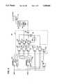
- FIG. 2An exemplary digital data receiver 10 for packet applications, such as in the network diagramed in FIG. 1, is shown in FIG. 2. It is understood that the invention embodied in the receiver 10, described herein, may be applicable to virtually any digital receiver application, such as the receiver (not shown) used by the repeater 3 (FIG. 1) to communicate on the backbone 2 or in burst mode satellite communication systems.
- the receiver 10has a decoder 11 which converts the input signals from medium 5, here a differential signal from a twisted pair, to digital data signals having uniform amplitude. If desired, the receiver 10 may also re-time the data.
- An exemplary decoder 11is a differential comparator (without retiming capability), such as that shown in U.S. Pat. No. 4,818,929, assigned to the same assignee as this invention.
- Squelch circuit 12is driven by slicers 13a, 13b, each having a slicing voltage of V TH .
- the slicing voltage, V THsets the minimum amplitude that each signal comprising the differential input signal from medium 5 must exceed to be considered a data signal and be applied to squelch 12.
- each slicer 13a, 13bconverts the differential input signals to two single-ended output signals. As will be shown in more detail below, if the differential input signals do not exceed the slicing limits, the outputs of the slicers 13a, 13b are "low". This creates a "dead zone" in input signal amplitudes that the slicers 13a, 13b will not respond to, thereby increasing the noise immunity of the receiver 10.
- the input signals from medium 5are described as differential, non-differential signals may be used.
- the squelch circuit 12relies on detecting positive-going and negative-going edges in the input signals and a means must be provided with non-differential input signals to generate positive and negative edge signals.
- the squelch circuit 12determines if a valid data signal is being received by the receiver 10. As determined by the squelch 12, if certain predetermined criteria for a valid data signal are met, the switch 14 closes and allows the decoded data from decoder 11 to pass.
- the predetermined criteriamay include, but is not limited to, a minimum number of transitions in the input signal and the frequency of the input signal being above a minimum frequency and/or below a maximum frequency, or a combination of the foregoing.
- the transitions necessary for the squelch 12 to operatemust also meet the frequency restrictions given above. The above is achieved by triggering a counter (not shown) within the squelch 12 when a first polarity transition in the input signal has occurred.
- the counterasserts a signal a predetermined time after being triggered, the predetermined time being the one-half of one cycle of a predetermined frequency. If the signal from the counter is asserted when an opposite polarity transition occurs, then the frequency of the input signal is less than the predetermined frequency. Conversely, if the signal is not asserted when the opposite polarity transition occurs, the frequency of the input signal is greater than the predetermined frequency. If, for example, two or more alternating polarity transitions occur meeting the desired frequency characteristics are received, then the received signal is probably a valid packet and the output of the decoder 11 is passed through switch 14.
- the data valid signalmay be cleared.
- the data valid signalmay be cleared by another circuit (not shown) at the end of the packet transmission.
- the following exemplary embodiment shown in FIGS. 3 and 4provides the above-described squelch function.
- the input signalis checked against both a minimum and maximum frequency limit as well as checking for a minimum number of alternating transitions, which meet the aforementioned frequency limits, for the acceptance of an input signal as a valid data packet. It is understood, however, that a subset of the aforementioned criteria may be implemented, reducing the number of circuit components described herein to implement the squelch function.
- FIG. 3the exemplary embodiment of the squelch circuit 12 (FIG. 2) is shown.
- Two substantially identical counters, 20a and 20bare triggered by a transition on the respective inputs A-IN and B-IN to the squelch 12.
- the counters 20a, 20bare triggered in response to opposite polarity transitions in the differential input signal to the receiver 10 (FIG. 2).
- the outputs EARLY, WINDOW, and LATE of the counters 20a, 20brelate to the significance of the next transition in the input signal (having an opposite polarity to the transition which triggered the enabled counter) when one of the outputs of counters 20a, 20b is asserted.
- next transitionoccurs when the EARLY signal is asserted, that transition occurred too soon, indicating the frequency of the input signal is too high.
- next transitionoccurs when the LATE signal is asserted, that transition occurred to late, indicating that the frequency of the input signal is too low.
- the next transitionoccurs when the WINDOW signal is asserted, the frequency of the input signal is within the desirable range.
- the details of the counters 20a, 20bare shown in FIG. 4 as counter 20 and illustrated in the timing diagram of FIG. 5.
- the counter 20produces the three output signals, EARLY, WINDOW, and LATE as a function of the count of the M-bit counter 40.
- the output of the counter 40drives a one-of-2 M decoder 41.
- the EARLY signalis asserted immediately after the counter 20 is triggered by an input signal to the input IN setting flip-flop 43. A predetermined time later, determined by which output of the decoder 41 is selected and the frequency of the clock to the counter 40 as will be discussed below, causes the WINDOW signal to be asserted and the EARLY signal is cleared.
- the outputs of decoder 41are pulses that are latched by flip-flops 44. All the outputs (EARLY, WINDOW, and LATE) are latched by flip-flops 45.
- a pulse to the RESET input of the counter 20clears the asserted outputs of the counter 20 by clearing flip-flop 43 which clears flip-flops 44, 45 and counter 40 to ready the counter 20 for a new input.
- the predetermined time intervalsare determined by which outputs of the decoder 41 are selected and the frequency of the clock to the counter 40.
- the clock frequencymay be derived from an external source, such as a master system clock (not shown) applied to the EXT CLK input, or from a gated ring oscillator 46 having a predetermined frequency of oscillation once enabled.
- the predetermined time intervalcorresponds to the highest frequency input signal the squelch 12 will accept.
- the other predetermined time interval(ending when the LATE signal is asserted) corresponds to the lowest frequency input signal the squelch 12 will accept.
- the corresponding predetermined time intervals for both counters 20a, 20b(FIG. 3) should be substantially the same.
- next edge detector (NED) 21which controls the operation of the counters 20a, 20b depending on the polarity of the most recent transition in the input signal.
- the NED 21has multiplexers 22 which select which counter 20a, 20b output is to be used for measuring the time to the next (opposite polarity) transition.
- the outputs of counter 20aare sampled by D-type flip-flops 23 when an opposite polarity transition occurs.
- Multiplexer 24couples the appropriate opposite polarity transition pulse from the inputs A-IN or B-IN to the clock inputs of the flip-flops 23 (from the B-IN input in this example) to control when the outputs of counter 20a are sampled by flip-flops 23.
- the outputs of the flip-flops 23are ORed together by OR gate 25, the output of which is delayed by delay 26, and the flip-flops 23 are cleared.
- the delayed clearing of the flip-flops 23generates a pulse at the output of OR gate 25 which clears the triggered counter, here counter 20a, through the demultiplexer 27.
- the N-bit counter 28is incremented. If, however, the transition occurs when the EARLY or LATE signal is asserted, the counter 28 is cleared by the ORing of the sampled signals from flip-flops 23 by OR gate 29.
- Counter 28counts the minimum number of sequential opposite polarity transitions in the input signal from medium 5 (FIG. 2) that meets the frequency criteria, discussed above. When a predetermined number of valid transitions occur, determined by the selection of the appropriate output of the decoder 30 and latched by flip-flop 31, the DATA VALID output signal from the squelch 12 is asserted.
- the configuration of the multiplexers 22, 24 and demultiplexer 27, to select which counter 20a, 20b output is to be sampled and which input transition is to trigger the sampling,is controlled by D-type flip-flop 32.
- Flip-flop 32samples the output of flip-flop 33 after the reset pulse from OR gate 25, through demultiplexer 27, clears the triggered counter 20a or 20b.
- Flip-flop 33stores which polarity transition occurred last (from the signal on corresponding input A-IN or B-IN) such that when flip-flop 32 is clocked after the reset pulse, the multiplexers 22, 24 and demultiplexer 27 are reconfigured.
- the received input signalis shown here as a differential signal corresponding to what would be received from medium 5 as shown in FIG. 2.
- the differential input signalhas at least two valid transitions and an invalid transition to illustrate the detection of a valid data signal and the result of detecting an invalid data signal.
- the differential input signalis shown starting from an idle state in which the signal amplitude was approximately zero (neither high nor low).
- the A-IN input to the squelch 12goes high when the received differential input signal goes sufficiently positive (exceeding V TH , a "high”) and goes low when the received signal goes negative (a "low”).
- the B-IN input signal to the squelch 12goes high and goes low when the received signal goes high.
- the signals to A-IN and B-IN inputsrepresent the received input signal being high and low, respectively. Note that when the differential input signal is idle, both A-IN and B-IN are low.
- the counter 20a in FIG. 3begins counting, asserting its output EARLY. After a predetermined interval of time, the WINDOW signal from the counter 20a is asserted, clearing the EARLY signal.
- a reset pulseA-RESET is applied to the counter 20a, clearing the WINDOW signal from counter 20a, while counter 20b begins counting.
- A-RESETa reset pulse
- the LATE output from counter 20bis asserted and then cleared by the positive transition in the input signal generating the B-RESET signal.
- the counter 20basserts its EARLY signal until a predetermined time later when the WINDOW signal is asserted, clearing the EARLY signal.
- the counter 20bis reset (B-RESET), and the counter 20a begins counting. Note that the LATE signal from counter 20b is not asserted.
- interval Cas discussed above in connection with interval A, the EARLY signal from counter 20a is asserted then cleared when the WINDOW signal is asserted thereby.
- the negative transition by the input signaltriggers counter 20b and clears counter 20a (A-RESET).
- the EARLY signalis asserted by counter 20b and then cleared when the WINDOW signal is asserted.
- the LATE signal from counter 20bis asserted clearing the WINDOW signal.
- the input signaltransitions positively, clearing the counter 20b (B-RESET) and starting the counter 20a. Since the positive transition in the input signal occurs when the LATE signal is asserted, the frequency of the input signal fails the minimum frequency criteria discussed above.
- select signal to the multiplexers 22, 24 and demultiplexer 27changes state with the falling edge of the reset pulses (A-RESET and B-RESET).
- the delay in changing stateassures that the pulses generated by the clearing of the flip-flops 23 using OR gate 25 and delay 26 are finished before the multiplexers 22, 24 and demultiplexer 27 are reconfigured.
- the predetermined time interval during which the EARLY signal is assertedis approximately 50 nanoseconds.
- the other predetermined time interval (ending when the LATE signal is asserted)is approximately 150 nanoseconds. This corresponds to a maximum frequency of approximately 10 MHz and a minimum frequency of approximately 3.33 MHz.
- DATA VALIDto be asserted, a minimum of two sequential alternating polarity transitions meeting the above frequency criteria must be received.
Landscapes
- Physics & Mathematics (AREA)
- Nonlinear Science (AREA)
- Engineering & Computer Science (AREA)
- Computer Networks & Wireless Communication (AREA)
- Signal Processing (AREA)
- Synchronisation In Digital Transmission Systems (AREA)
Abstract
Description
Claims (14)
Priority Applications (1)
| Application Number | Priority Date | Filing Date | Title |
|---|---|---|---|
| US07/515,293US5199049A (en) | 1990-04-27 | 1990-04-27 | Circuit and method of digital carrier detection for burst mode communication systems |
Applications Claiming Priority (1)
| Application Number | Priority Date | Filing Date | Title |
|---|---|---|---|
| US07/515,293US5199049A (en) | 1990-04-27 | 1990-04-27 | Circuit and method of digital carrier detection for burst mode communication systems |
Publications (1)
| Publication Number | Publication Date |
|---|---|
| US5199049Atrue US5199049A (en) | 1993-03-30 |
Family
ID=24050756
Family Applications (1)
| Application Number | Title | Priority Date | Filing Date |
|---|---|---|---|
| US07/515,293Expired - LifetimeUS5199049A (en) | 1990-04-27 | 1990-04-27 | Circuit and method of digital carrier detection for burst mode communication systems |
Country Status (1)
| Country | Link |
|---|---|
| US (1) | US5199049A (en) |
Cited By (60)
| Publication number | Priority date | Publication date | Assignee | Title |
|---|---|---|---|---|
| US5317215A (en)* | 1992-12-01 | 1994-05-31 | 3Com Corporation | Method and apparatus for frequency discriminating computer network signals |
| US5418821A (en)* | 1991-10-15 | 1995-05-23 | National Semiconductor Corporation | Method and apparatus for sample-data receiver squelch |
| US5509006A (en)* | 1994-04-18 | 1996-04-16 | Cisco Systems Incorporated | Apparatus and method for switching packets using tree memory |
| US5519704A (en)* | 1994-04-21 | 1996-05-21 | Cisco Systems, Inc. | Reliable transport protocol for internetwork routing |
| GB2296408A (en)* | 1994-12-23 | 1996-06-26 | Motorola Inc | Signal quality detection in a digital communication system; muting control |
| US5717720A (en)* | 1994-12-13 | 1998-02-10 | Lucent Technologies Inc. | Digital data receivers, methods and circuitry for differentiating between transmitted signals of varying physical protocols and frequencies |
| US5867666A (en)* | 1994-12-29 | 1999-02-02 | Cisco Systems, Inc. | Virtual interfaces with dynamic binding |
| US5946305A (en)* | 1994-12-13 | 1999-08-31 | Sony Corporation | Cordless telephone system |
| US6035105A (en)* | 1996-01-02 | 2000-03-07 | Cisco Technology, Inc. | Multiple VLAN architecture system |
| US6078590A (en)* | 1997-07-14 | 2000-06-20 | Cisco Technology, Inc. | Hierarchical routing knowledge for multicast packet routing |
| US6091725A (en)* | 1995-12-29 | 2000-07-18 | Cisco Systems, Inc. | Method for traffic management, traffic prioritization, access control, and packet forwarding in a datagram computer network |
| US6097718A (en)* | 1996-01-02 | 2000-08-01 | Cisco Technology, Inc. | Snapshot routing with route aging |
| US6101115A (en)* | 1998-08-07 | 2000-08-08 | Cisco Technology, Inc. | CAM match line precharge |
| US6111877A (en)* | 1997-12-31 | 2000-08-29 | Cisco Technology, Inc. | Load sharing across flows |
| US6122272A (en)* | 1997-05-23 | 2000-09-19 | Cisco Technology, Inc. | Call size feedback on PNNI operation |
| US6157641A (en)* | 1997-08-22 | 2000-12-05 | Cisco Technology, Inc. | Multiprotocol packet recognition and switching |
| US6182224B1 (en) | 1995-09-29 | 2001-01-30 | Cisco Systems, Inc. | Enhanced network services using a subnetwork of communicating processors |
| US6182147B1 (en) | 1998-07-31 | 2001-01-30 | Cisco Technology, Inc. | Multicast group routing using unidirectional links |
| US6212183B1 (en) | 1997-08-22 | 2001-04-03 | Cisco Technology, Inc. | Multiple parallel packet routing lookup |
| US6212182B1 (en) | 1996-06-27 | 2001-04-03 | Cisco Technology, Inc. | Combined unicast and multicast scheduling |
| US6243667B1 (en) | 1996-05-28 | 2001-06-05 | Cisco Systems, Inc. | Network flow switching and flow data export |
| US6246268B1 (en) | 2000-06-07 | 2001-06-12 | Marvell International Ltd. | CMOS integrated signal detection circuit with high efficiency and performance |
| US6295356B1 (en) | 1998-03-26 | 2001-09-25 | Cisco Technology, Inc. | Power feed for network devices |
| US6304546B1 (en) | 1996-12-19 | 2001-10-16 | Cisco Technology, Inc. | End-to-end bidirectional keep-alive using virtual circuits |
| US6308148B1 (en) | 1996-05-28 | 2001-10-23 | Cisco Technology, Inc. | Network flow data export |
| US6308219B1 (en) | 1998-07-31 | 2001-10-23 | Cisco Technology, Inc. | Routing table lookup implemented using M-trie having nodes duplicated in multiple memory banks |
| US6330599B1 (en) | 1997-08-05 | 2001-12-11 | Cisco Technology, Inc. | Virtual interfaces with dynamic binding |
| US6343072B1 (en) | 1997-10-01 | 2002-01-29 | Cisco Technology, Inc. | Single-chip architecture for shared-memory router |
| US6356530B1 (en) | 1997-05-23 | 2002-03-12 | Cisco Technology, Inc. | Next hop selection in ATM networks |
| US6370121B1 (en) | 1998-06-29 | 2002-04-09 | Cisco Technology, Inc. | Method and system for shortcut trunking of LAN bridges |
| US6377577B1 (en) | 1998-06-30 | 2002-04-23 | Cisco Technology, Inc. | Access control list processing in hardware |
| US6389506B1 (en) | 1998-08-07 | 2002-05-14 | Cisco Technology, Inc. | Block mask ternary cam |
| US20020063584A1 (en)* | 2000-11-29 | 2002-05-30 | James Molenda | Unpowered twisted pair loopback circuit for differential mode signaling |
| US20020097736A1 (en)* | 1998-04-01 | 2002-07-25 | Earl Cohen | Route/service processor scalability via flow-based distribution of traffic |
| US6434120B1 (en) | 1998-08-25 | 2002-08-13 | Cisco Technology, Inc. | Autosensing LMI protocols in frame relay networks |
| US6446230B1 (en) | 1998-09-14 | 2002-09-03 | Cisco Technology, Inc. | Mechanism for enabling compliance with the IEEE standard 1149.1 for boundary-scan designs and tests |
| US6512766B2 (en) | 1997-08-22 | 2003-01-28 | Cisco Systems, Inc. | Enhanced internet packet routing lookup |
| US6603772B1 (en) | 1999-03-31 | 2003-08-05 | Cisco Technology, Inc. | Multicast routing with multicast virtual output queues and shortest queue first allocation |
| US20040062203A1 (en)* | 1998-04-10 | 2004-04-01 | Austermann John F. | System for communicating with electronic equipment |
| US6751236B1 (en) | 2000-12-15 | 2004-06-15 | Cisco Technology, Inc. | Configurable channel associated signaling (“CAS”) line signaling using plain text strings |
| US6757791B1 (en) | 1999-03-30 | 2004-06-29 | Cisco Technology, Inc. | Method and apparatus for reordering packet data units in storage queues for reading and writing memory |
| US6760331B1 (en) | 1999-03-31 | 2004-07-06 | Cisco Technology, Inc. | Multicast routing with nearest queue first allocation and dynamic and static vector quantization |
| US20040130438A1 (en)* | 2002-10-08 | 2004-07-08 | Colder Products Company | Data collision detection device and method |
| US6771642B1 (en) | 1999-01-08 | 2004-08-03 | Cisco Technology, Inc. | Method and apparatus for scheduling packets in a packet switch |
| US6831923B1 (en) | 1995-08-04 | 2004-12-14 | Cisco Technology, Inc. | Pipelined multiple issue packet switch |
| US20050141415A1 (en)* | 1997-12-05 | 2005-06-30 | Cisco Technology, Inc., A California Corporation | Extending SONET/SDH automatic protection switching |
| US6917966B1 (en) | 1995-09-29 | 2005-07-12 | Cisco Technology, Inc. | Enhanced network services using a subnetwork of communicating processors |
| US6920112B1 (en) | 1998-06-29 | 2005-07-19 | Cisco Technology, Inc. | Sampling packets for network monitoring |
| US20050268120A1 (en)* | 2004-05-13 | 2005-12-01 | Schindler Frederick R | Power delivery over ethernet cables |
| US7026730B1 (en) | 2002-12-20 | 2006-04-11 | Cisco Technology, Inc. | Integrated connector unit |
| US20060112288A1 (en)* | 2004-11-24 | 2006-05-25 | Schindler Frederick R | Increased power for power over ethernet applications |
| US7061142B1 (en) | 2003-05-28 | 2006-06-13 | Cisco Technology, Inc. | Inline power device detection |
| US7065762B1 (en) | 1999-03-22 | 2006-06-20 | Cisco Technology, Inc. | Method, apparatus and computer program product for borrowed-virtual-time scheduling |
| US20060149978A1 (en)* | 2005-01-04 | 2006-07-06 | Randall Anthony L | Method and system for managing power delivery for power over ethernet systems |
| US7076543B1 (en) | 2002-02-13 | 2006-07-11 | Cisco Technology, Inc. | Method and apparatus for collecting, aggregating and monitoring network management information |
| US7099463B1 (en) | 2000-11-09 | 2006-08-29 | Cisco Technology, Inc. | Method and apparatus for detecting a compatible phantom powered device using common mode signaling |
| US7116669B1 (en) | 1997-06-17 | 2006-10-03 | Cisco Technology, Inc. | Format for automatic generation of unique ATM addresses used for PNNI |
| US7246148B1 (en) | 1995-09-29 | 2007-07-17 | Cisco Technology, Inc. | Enhanced network services using a subnetwork of communicating processors |
| US7286525B1 (en) | 1997-12-31 | 2007-10-23 | Cisco Technology, Inc. | Synchronous pipelined switch using serial transmission |
| US7366297B1 (en) | 2003-05-21 | 2008-04-29 | Cisco Technology, Inc. | Method and system for converting alternating current to ethernet in-line power |
Citations (12)
| Publication number | Priority date | Publication date | Assignee | Title |
|---|---|---|---|---|
| US3437937A (en)* | 1966-08-08 | 1969-04-08 | Wilcox Electric Co Inc | Digital squelch system |
| US3633112A (en)* | 1970-09-28 | 1972-01-04 | Collins Radio Co | Digital audio squelch |
| US3852671A (en)* | 1973-06-25 | 1974-12-03 | Gte Sylvania Inc | Communication receiving apparatus employing several samples of baseboard noise to detect an incoming signal and turn on the apparatus |
| US3873925A (en)* | 1974-03-07 | 1975-03-25 | Motorola Inc | Audio frequency squelch system |
| US3902123A (en)* | 1973-11-30 | 1975-08-26 | Cincinnati Electronics Corp | Digital circuit for determining if signal source consists primarily of noise or contains information |
| US3939431A (en)* | 1974-11-25 | 1976-02-17 | Motorola, Inc. | Muting circuit for a radio receiver |
| US3939425A (en)* | 1973-09-28 | 1976-02-17 | Sony Corporation | Noise-squelching circuit using a phase-locked loop |
| US4344175A (en)* | 1980-12-22 | 1982-08-10 | General Electric Company | Muting circuit |
| US4445092A (en)* | 1980-09-30 | 1984-04-24 | Sony Corporation | Periodic pulse forming circuit |
| US4458204A (en)* | 1981-09-10 | 1984-07-03 | Weber Harold J | Frequency dependent pulsed gain modulated concealed structure locator |
| US4630290A (en)* | 1983-11-18 | 1986-12-16 | Nec Corporation | Squelch signal generator capable of generating a squelch signal with a high reliability |
| US4815108A (en)* | 1987-06-26 | 1989-03-21 | Mitsubishi Denki Kabushiki Kaisha | Signal detection apparatus |
- 1990
- 1990-04-27USUS07/515,293patent/US5199049A/ennot_activeExpired - Lifetime
Patent Citations (12)
| Publication number | Priority date | Publication date | Assignee | Title |
|---|---|---|---|---|
| US3437937A (en)* | 1966-08-08 | 1969-04-08 | Wilcox Electric Co Inc | Digital squelch system |
| US3633112A (en)* | 1970-09-28 | 1972-01-04 | Collins Radio Co | Digital audio squelch |
| US3852671A (en)* | 1973-06-25 | 1974-12-03 | Gte Sylvania Inc | Communication receiving apparatus employing several samples of baseboard noise to detect an incoming signal and turn on the apparatus |
| US3939425A (en)* | 1973-09-28 | 1976-02-17 | Sony Corporation | Noise-squelching circuit using a phase-locked loop |
| US3902123A (en)* | 1973-11-30 | 1975-08-26 | Cincinnati Electronics Corp | Digital circuit for determining if signal source consists primarily of noise or contains information |
| US3873925A (en)* | 1974-03-07 | 1975-03-25 | Motorola Inc | Audio frequency squelch system |
| US3939431A (en)* | 1974-11-25 | 1976-02-17 | Motorola, Inc. | Muting circuit for a radio receiver |
| US4445092A (en)* | 1980-09-30 | 1984-04-24 | Sony Corporation | Periodic pulse forming circuit |
| US4344175A (en)* | 1980-12-22 | 1982-08-10 | General Electric Company | Muting circuit |
| US4458204A (en)* | 1981-09-10 | 1984-07-03 | Weber Harold J | Frequency dependent pulsed gain modulated concealed structure locator |
| US4630290A (en)* | 1983-11-18 | 1986-12-16 | Nec Corporation | Squelch signal generator capable of generating a squelch signal with a high reliability |
| US4815108A (en)* | 1987-06-26 | 1989-03-21 | Mitsubishi Denki Kabushiki Kaisha | Signal detection apparatus |
Non-Patent Citations (4)
| Title |
|---|
| "DP83922 Twisted Pair Transceiver Interface (TPI)", National Semiconductor, Dec. 1989, pp. 1-15. |
| "Draft Supplement to IEEE Std 802.3, CSMA/CD Access Method and Physical Layer Specifications", IEEE Std. 802.3, Type 10BASE-T Pat Thaler, Feb. 15, 1990 pp. 1-29. |
| DP83922 Twisted Pair Transceiver Interface (TPI) , National Semiconductor, Dec. 1989, pp. 1 15.* |
| Draft Supplement to IEEE Std 802.3, CSMA/CD Access Method and Physical Layer Specifications , IEEE Std. 802.3, Type 10BASE T Pat Thaler, Feb. 15, 1990 pp. 1 29.* |
Cited By (100)
| Publication number | Priority date | Publication date | Assignee | Title |
|---|---|---|---|---|
| US5418821A (en)* | 1991-10-15 | 1995-05-23 | National Semiconductor Corporation | Method and apparatus for sample-data receiver squelch |
| WO1994012888A1 (en)* | 1992-12-01 | 1994-06-09 | 3Com Corporation | Method and apparatus for discriminating computer network signals |
| US5317215A (en)* | 1992-12-01 | 1994-05-31 | 3Com Corporation | Method and apparatus for frequency discriminating computer network signals |
| US5509006A (en)* | 1994-04-18 | 1996-04-16 | Cisco Systems Incorporated | Apparatus and method for switching packets using tree memory |
| US5519704A (en)* | 1994-04-21 | 1996-05-21 | Cisco Systems, Inc. | Reliable transport protocol for internetwork routing |
| CN1079626C (en)* | 1994-12-13 | 2002-02-20 | 索尼公司 | Cordless telephone system |
| US5717720A (en)* | 1994-12-13 | 1998-02-10 | Lucent Technologies Inc. | Digital data receivers, methods and circuitry for differentiating between transmitted signals of varying physical protocols and frequencies |
| US5946305A (en)* | 1994-12-13 | 1999-08-31 | Sony Corporation | Cordless telephone system |
| GB2296408A (en)* | 1994-12-23 | 1996-06-26 | Motorola Inc | Signal quality detection in a digital communication system; muting control |
| GB2296408B (en)* | 1994-12-23 | 1999-04-28 | Motorola Inc | Method and apparatus for signal quality detection in a communication system |
| US5867666A (en)* | 1994-12-29 | 1999-02-02 | Cisco Systems, Inc. | Virtual interfaces with dynamic binding |
| US6327251B1 (en) | 1995-08-03 | 2001-12-04 | Cisco Technology, Inc. | Snapshot routing |
| US6831923B1 (en) | 1995-08-04 | 2004-12-14 | Cisco Technology, Inc. | Pipelined multiple issue packet switch |
| US6917966B1 (en) | 1995-09-29 | 2005-07-12 | Cisco Technology, Inc. | Enhanced network services using a subnetwork of communicating processors |
| US7246148B1 (en) | 1995-09-29 | 2007-07-17 | Cisco Technology, Inc. | Enhanced network services using a subnetwork of communicating processors |
| US6182224B1 (en) | 1995-09-29 | 2001-01-30 | Cisco Systems, Inc. | Enhanced network services using a subnetwork of communicating processors |
| US6640243B1 (en) | 1995-09-29 | 2003-10-28 | Cisco Technology, Inc. | Enhanced network services using a subnetwork of communicating processors |
| US6798776B1 (en) | 1995-12-29 | 2004-09-28 | Cisco Technology, Inc. | Method for traffic management, traffic prioritization, access control, and packet forwarding in a datagram computer network |
| US8401027B2 (en) | 1995-12-29 | 2013-03-19 | Cisco Technology, Inc. | Method for traffic management, traffic prioritization, access control, and packet forwarding in a datagram computer network |
| US7443858B1 (en) | 1995-12-29 | 2008-10-28 | Cisco Technology, Inc. | Method for traffic management, traffic prioritization, access control, and packet forwarding in a datagram computer network |
| US6091725A (en)* | 1995-12-29 | 2000-07-18 | Cisco Systems, Inc. | Method for traffic management, traffic prioritization, access control, and packet forwarding in a datagram computer network |
| US20090046734A1 (en)* | 1995-12-29 | 2009-02-19 | Cisco Technology, Inc. | Method for Traffic Management, Traffic Prioritization, Access Control, and Packet Forwarding in a Datagram Computer Network |
| US6097718A (en)* | 1996-01-02 | 2000-08-01 | Cisco Technology, Inc. | Snapshot routing with route aging |
| US6035105A (en)* | 1996-01-02 | 2000-03-07 | Cisco Technology, Inc. | Multiple VLAN architecture system |
| US6219699B1 (en) | 1996-01-02 | 2001-04-17 | Cisco Technologies, Inc. | Multiple VLAN Architecture system |
| US20050027506A1 (en)* | 1996-05-28 | 2005-02-03 | Kerr Darren R. | Method network flow switching and flow data export |
| US6889181B2 (en) | 1996-05-28 | 2005-05-03 | Cisco Technology, Inc. | Network flow switching and flow data export |
| US6308148B1 (en) | 1996-05-28 | 2001-10-23 | Cisco Technology, Inc. | Network flow data export |
| US7475156B2 (en) | 1996-05-28 | 2009-01-06 | Cisco Technology, Inc. | Network flow switching and flow data export |
| US7260518B2 (en) | 1996-05-28 | 2007-08-21 | Cisco Technology, Inc. | Network flow switching and flow data report |
| US6243667B1 (en) | 1996-05-28 | 2001-06-05 | Cisco Systems, Inc. | Network flow switching and flow data export |
| US6212182B1 (en) | 1996-06-27 | 2001-04-03 | Cisco Technology, Inc. | Combined unicast and multicast scheduling |
| US20020163891A1 (en)* | 1996-06-28 | 2002-11-07 | Cisco Systems, Inc., A California Corporation | Autosensing LMI protocols in frame relay networks |
| US7103007B2 (en) | 1996-06-28 | 2006-09-05 | Cisco Technology, Inc. | Autosensing LMI protocols in frame relay networks |
| US6304546B1 (en) | 1996-12-19 | 2001-10-16 | Cisco Technology, Inc. | End-to-end bidirectional keep-alive using virtual circuits |
| US6538988B1 (en) | 1996-12-19 | 2003-03-25 | Cisco Technology, Inc. | End-to-end bidirectional keep-alive using virtual circuits |
| US6356530B1 (en) | 1997-05-23 | 2002-03-12 | Cisco Technology, Inc. | Next hop selection in ATM networks |
| US6122272A (en)* | 1997-05-23 | 2000-09-19 | Cisco Technology, Inc. | Call size feedback on PNNI operation |
| US7116669B1 (en) | 1997-06-17 | 2006-10-03 | Cisco Technology, Inc. | Format for automatic generation of unique ATM addresses used for PNNI |
| US6078590A (en)* | 1997-07-14 | 2000-06-20 | Cisco Technology, Inc. | Hierarchical routing knowledge for multicast packet routing |
| US6611528B1 (en) | 1997-07-14 | 2003-08-26 | Cisco Technology, Inc. | Hierarchical routing knowledge for multicast packet routing |
| US6330599B1 (en) | 1997-08-05 | 2001-12-11 | Cisco Technology, Inc. | Virtual interfaces with dynamic binding |
| US6512766B2 (en) | 1997-08-22 | 2003-01-28 | Cisco Systems, Inc. | Enhanced internet packet routing lookup |
| US6157641A (en)* | 1997-08-22 | 2000-12-05 | Cisco Technology, Inc. | Multiprotocol packet recognition and switching |
| US6212183B1 (en) | 1997-08-22 | 2001-04-03 | Cisco Technology, Inc. | Multiple parallel packet routing lookup |
| US6343072B1 (en) | 1997-10-01 | 2002-01-29 | Cisco Technology, Inc. | Single-chip architecture for shared-memory router |
| US20050141415A1 (en)* | 1997-12-05 | 2005-06-30 | Cisco Technology, Inc., A California Corporation | Extending SONET/SDH automatic protection switching |
| US7570583B2 (en) | 1997-12-05 | 2009-08-04 | Cisco Technology, Inc. | Extending SONET/SDH automatic protection switching |
| US6111877A (en)* | 1997-12-31 | 2000-08-29 | Cisco Technology, Inc. | Load sharing across flows |
| US7286525B1 (en) | 1997-12-31 | 2007-10-23 | Cisco Technology, Inc. | Synchronous pipelined switch using serial transmission |
| US6603765B1 (en) | 1997-12-31 | 2003-08-05 | Cisco Technology, Inc. | Load sharing across flows |
| US6295356B1 (en) | 1998-03-26 | 2001-09-25 | Cisco Technology, Inc. | Power feed for network devices |
| US20020097736A1 (en)* | 1998-04-01 | 2002-07-25 | Earl Cohen | Route/service processor scalability via flow-based distribution of traffic |
| US6853638B2 (en) | 1998-04-01 | 2005-02-08 | Cisco Technology, Inc. | Route/service processor scalability via flow-based distribution of traffic |
| US9812825B2 (en) | 1998-04-10 | 2017-11-07 | Chrimar Systems, Inc. | Ethernet device |
| US9049019B2 (en) | 1998-04-10 | 2015-06-02 | Chrimar Systems, Inc. | Network equipment and optional tether |
| US9019838B2 (en) | 1998-04-10 | 2015-04-28 | Chrimar Systems, Inc. | Central piece of network equipment |
| US8942107B2 (en) | 1998-04-10 | 2015-01-27 | Chrimar Systems, Inc. | Piece of ethernet terminal equipment |
| US20040062203A1 (en)* | 1998-04-10 | 2004-04-01 | Austermann John F. | System for communicating with electronic equipment |
| US8902760B2 (en) | 1998-04-10 | 2014-12-02 | Chrimar Systems, Inc. | Network system and optional tethers |
| US8155012B2 (en) | 1998-04-10 | 2012-04-10 | Chrimar Systems, Inc. | System and method for adapting a piece of terminal equipment |
| US6370121B1 (en) | 1998-06-29 | 2002-04-09 | Cisco Technology, Inc. | Method and system for shortcut trunking of LAN bridges |
| US6920112B1 (en) | 1998-06-29 | 2005-07-19 | Cisco Technology, Inc. | Sampling packets for network monitoring |
| US6377577B1 (en) | 1998-06-30 | 2002-04-23 | Cisco Technology, Inc. | Access control list processing in hardware |
| US6182147B1 (en) | 1998-07-31 | 2001-01-30 | Cisco Technology, Inc. | Multicast group routing using unidirectional links |
| US6308219B1 (en) | 1998-07-31 | 2001-10-23 | Cisco Technology, Inc. | Routing table lookup implemented using M-trie having nodes duplicated in multiple memory banks |
| US6101115A (en)* | 1998-08-07 | 2000-08-08 | Cisco Technology, Inc. | CAM match line precharge |
| US6389506B1 (en) | 1998-08-07 | 2002-05-14 | Cisco Technology, Inc. | Block mask ternary cam |
| US6434120B1 (en) | 1998-08-25 | 2002-08-13 | Cisco Technology, Inc. | Autosensing LMI protocols in frame relay networks |
| US6560739B1 (en) | 1998-09-14 | 2003-05-06 | Cisco Technology, Inc. | Mechanism for enabling compliance with the IEEE standard 1149.1 for boundary-scan designs and tests |
| US6446230B1 (en) | 1998-09-14 | 2002-09-03 | Cisco Technology, Inc. | Mechanism for enabling compliance with the IEEE standard 1149.1 for boundary-scan designs and tests |
| US6771642B1 (en) | 1999-01-08 | 2004-08-03 | Cisco Technology, Inc. | Method and apparatus for scheduling packets in a packet switch |
| US7065762B1 (en) | 1999-03-22 | 2006-06-20 | Cisco Technology, Inc. | Method, apparatus and computer program product for borrowed-virtual-time scheduling |
| US6757791B1 (en) | 1999-03-30 | 2004-06-29 | Cisco Technology, Inc. | Method and apparatus for reordering packet data units in storage queues for reading and writing memory |
| US6760331B1 (en) | 1999-03-31 | 2004-07-06 | Cisco Technology, Inc. | Multicast routing with nearest queue first allocation and dynamic and static vector quantization |
| US6603772B1 (en) | 1999-03-31 | 2003-08-05 | Cisco Technology, Inc. | Multicast routing with multicast virtual output queues and shortest queue first allocation |
| US6246268B1 (en) | 2000-06-07 | 2001-06-12 | Marvell International Ltd. | CMOS integrated signal detection circuit with high efficiency and performance |
| US7099463B1 (en) | 2000-11-09 | 2006-08-29 | Cisco Technology, Inc. | Method and apparatus for detecting a compatible phantom powered device using common mode signaling |
| US7447307B2 (en) | 2000-11-29 | 2008-11-04 | Cisco Technology, Inc. | Unpowered twisted pair loopback circuit for differential mode signaling |
| US20090129583A1 (en)* | 2000-11-29 | 2009-05-21 | Cisco Technology, Inc. A California Corporation | Unpowered twisted pair loopback circuit for differential mode signaling |
| US20020063584A1 (en)* | 2000-11-29 | 2002-05-30 | James Molenda | Unpowered twisted pair loopback circuit for differential mode signaling |
| US8094808B2 (en) | 2000-11-29 | 2012-01-10 | Cisco Technology, Inc. | Unpowered twisted pair loopback circuit for differential mode signaling |
| US6751236B1 (en) | 2000-12-15 | 2004-06-15 | Cisco Technology, Inc. | Configurable channel associated signaling (“CAS”) line signaling using plain text strings |
| US7318094B1 (en) | 2002-02-13 | 2008-01-08 | Cisco Technology, Inc. | Apparatus, system and device for collecting, aggregating and monitoring network management information |
| US7076543B1 (en) | 2002-02-13 | 2006-07-11 | Cisco Technology, Inc. | Method and apparatus for collecting, aggregating and monitoring network management information |
| US7352771B2 (en)* | 2002-10-08 | 2008-04-01 | Colder Products Company | Data collision detection device and method |
| US20040130438A1 (en)* | 2002-10-08 | 2004-07-08 | Colder Products Company | Data collision detection device and method |
| US7026730B1 (en) | 2002-12-20 | 2006-04-11 | Cisco Technology, Inc. | Integrated connector unit |
| US20060175905A1 (en)* | 2002-12-20 | 2006-08-10 | Cisco Technology, Inc., A California Corporation | Integrated Connector Unit |
| US7366297B1 (en) | 2003-05-21 | 2008-04-29 | Cisco Technology, Inc. | Method and system for converting alternating current to ethernet in-line power |
| US7061142B1 (en) | 2003-05-28 | 2006-06-13 | Cisco Technology, Inc. | Inline power device detection |
| US7603570B2 (en) | 2004-05-13 | 2009-10-13 | Cisco Technology, Inc. | Power delivery over ethernet cables |
| US7921314B2 (en) | 2004-05-13 | 2011-04-05 | Cisco Technology, Inc. | Providing power over ethernet cables |
| US20050268120A1 (en)* | 2004-05-13 | 2005-12-01 | Schindler Frederick R | Power delivery over ethernet cables |
| US7373528B2 (en) | 2004-11-24 | 2008-05-13 | Cisco Technology, Inc. | Increased power for power over Ethernet applications |
| US20060112288A1 (en)* | 2004-11-24 | 2006-05-25 | Schindler Frederick R | Increased power for power over ethernet applications |
| US7509505B2 (en) | 2005-01-04 | 2009-03-24 | Cisco Technology, Inc. | Method and system for managing power delivery for power over Ethernet systems |
| US8082457B2 (en) | 2005-01-04 | 2011-12-20 | Cisco Technology, Inc. | Data communications device for communicating with and concurrently providing power to a set of powerable devices |
| US20080288794A1 (en)* | 2005-01-04 | 2008-11-20 | Cisco Technology, Inc. | Method and system for managing power delivery for power over ethernet systems |
| US20060149978A1 (en)* | 2005-01-04 | 2006-07-06 | Randall Anthony L | Method and system for managing power delivery for power over ethernet systems |
Similar Documents
| Publication | Publication Date | Title |
|---|---|---|
| US5199049A (en) | Circuit and method of digital carrier detection for burst mode communication systems | |
| US5648956A (en) | Apparatus and method for full-duplex ethernet communications | |
| US4197502A (en) | Digital signal detector | |
| EP0679307B1 (en) | Delay line separator for data bus | |
| US5692166A (en) | Method and system for resynchronizing a phase-shifted received data stream with a master clock | |
| US8572200B2 (en) | Master/slave decision device and master/slave decision method applied to network device | |
| US5157651A (en) | Apparatus and method for determining line rates | |
| US5317215A (en) | Method and apparatus for frequency discriminating computer network signals | |
| JP3036854B2 (en) | Interference detection circuit | |
| US5373508A (en) | Detecting valid data from a twisted pair medium | |
| JP2812665B2 (en) | Data collision detection circuit and detection method for communication network | |
| JPH06177862A (en) | Method and apparatus for averaging of pulses in flow of pulses | |
| US5717720A (en) | Digital data receivers, methods and circuitry for differentiating between transmitted signals of varying physical protocols and frequencies | |
| US4908530A (en) | Non-linear squelch circuit for IEEE-802. 3 protocol | |
| US5418821A (en) | Method and apparatus for sample-data receiver squelch | |
| US5903616A (en) | Synchronous clock multiplexer | |
| CA1217564A (en) | Serial to parallel data conversion circuit | |
| US7260164B2 (en) | Efficient filtering of RxLOS signal in SerDes applications | |
| US5631709A (en) | Method and apparatus for processing a composite synchronizing signal | |
| CA2052811C (en) | Framing bit sequence detection in digital data communication systems | |
| US6810024B1 (en) | Auto-detection system and method for a network transceiver | |
| JPH07212413A (en) | Asynchronous data receiving circuit | |
| EP0490002B1 (en) | A flag counter circuit | |
| JPH0746243A (en) | Aui loopback detector |
Legal Events
| Date | Code | Title | Description |
|---|---|---|---|
| AS | Assignment | Owner name:AMERICAN TELEPHONE AND TELEGRAPH COMPANY, NEW YORK Free format text:ASSIGNMENT OF ASSIGNORS INTEREST.;ASSIGNOR:WILSON, WILLIAM B.;REEL/FRAME:005292/0332 Effective date:19900427 | |
| STCF | Information on status: patent grant | Free format text:PATENTED CASE | |
| REFU | Refund | Free format text:REFUND PROCESSED. MAINTENANCE FEE HAS ALREADY BEEN PAID (ORIGINAL EVENT CODE: R160); ENTITY STATUS OF PATENT OWNER: LARGE ENTITY | |
| FEPP | Fee payment procedure | Free format text:PAYOR NUMBER ASSIGNED (ORIGINAL EVENT CODE: ASPN); ENTITY STATUS OF PATENT OWNER: LARGE ENTITY | |
| FPAY | Fee payment | Year of fee payment:4 | |
| FEPP | Fee payment procedure | Free format text:PAYOR NUMBER ASSIGNED (ORIGINAL EVENT CODE: ASPN); ENTITY STATUS OF PATENT OWNER: LARGE ENTITY Free format text:PAYER NUMBER DE-ASSIGNED (ORIGINAL EVENT CODE: RMPN); ENTITY STATUS OF PATENT OWNER: LARGE ENTITY | |
| FPAY | Fee payment | Year of fee payment:8 | |
| FEPP | Fee payment procedure | Free format text:PAYOR NUMBER ASSIGNED (ORIGINAL EVENT CODE: ASPN); ENTITY STATUS OF PATENT OWNER: LARGE ENTITY Free format text:PAYER NUMBER DE-ASSIGNED (ORIGINAL EVENT CODE: RMPN); ENTITY STATUS OF PATENT OWNER: LARGE ENTITY | |
| FPAY | Fee payment | Year of fee payment:12 |