US5198963A - Multiple integrated circuit module which simplifies handling and testing - Google Patents
Multiple integrated circuit module which simplifies handling and testingDownload PDFInfo
- Publication number
- US5198963A US5198963AUS07/795,440US79544091AUS5198963AUS 5198963 AUS5198963 AUS 5198963AUS 79544091 AUS79544091 AUS 79544091AUS 5198963 AUS5198963 AUS 5198963A
- Authority
- US
- United States
- Prior art keywords
- integrated circuit
- contact points
- module
- module substrate
- bridge chip
- Prior art date
- Legal status (The legal status is an assumption and is not a legal conclusion. Google has not performed a legal analysis and makes no representation as to the accuracy of the status listed.)
- Expired - Lifetime
Links
Images

Classifications
- G—PHYSICS
- G01—MEASURING; TESTING
- G01R—MEASURING ELECTRIC VARIABLES; MEASURING MAGNETIC VARIABLES
- G01R31/00—Arrangements for testing electric properties; Arrangements for locating electric faults; Arrangements for electrical testing characterised by what is being tested not provided for elsewhere
- G01R31/28—Testing of electronic circuits, e.g. by signal tracer
- G01R31/2851—Testing of integrated circuits [IC]
- G01R31/2855—Environmental, reliability or burn-in testing
- G01R31/286—External aspects, e.g. related to chambers, contacting devices or handlers
- G01R31/2863—Contacting devices, e.g. sockets, burn-in boards or mounting fixtures
- G—PHYSICS
- G01—MEASURING; TESTING
- G01R—MEASURING ELECTRIC VARIABLES; MEASURING MAGNETIC VARIABLES
- G01R31/00—Arrangements for testing electric properties; Arrangements for locating electric faults; Arrangements for electrical testing characterised by what is being tested not provided for elsewhere
- G01R31/28—Testing of electronic circuits, e.g. by signal tracer
- G01R31/2851—Testing of integrated circuits [IC]
- G01R31/2886—Features relating to contacting the IC under test, e.g. probe heads; chucks
- H—ELECTRICITY
- H01—ELECTRIC ELEMENTS
- H01L—SEMICONDUCTOR DEVICES NOT COVERED BY CLASS H10
- H01L22/00—Testing or measuring during manufacture or treatment; Reliability measurements, i.e. testing of parts without further processing to modify the parts as such; Structural arrangements therefor
- H01L22/20—Sequence of activities consisting of a plurality of measurements, corrections, marking or sorting steps
- H—ELECTRICITY
- H01—ELECTRIC ELEMENTS
- H01L—SEMICONDUCTOR DEVICES NOT COVERED BY CLASS H10
- H01L23/00—Details of semiconductor or other solid state devices
- H01L23/52—Arrangements for conducting electric current within the device in operation from one component to another, i.e. interconnections, e.g. wires, lead frames
- H01L23/538—Arrangements for conducting electric current within the device in operation from one component to another, i.e. interconnections, e.g. wires, lead frames the interconnection structure between a plurality of semiconductor chips being formed on, or in, insulating substrates
- H01L23/5385—Assembly of a plurality of insulating substrates
- H—ELECTRICITY
- H01—ELECTRIC ELEMENTS
- H01L—SEMICONDUCTOR DEVICES NOT COVERED BY CLASS H10
- H01L25/00—Assemblies consisting of a plurality of semiconductor or other solid state devices
- H01L25/03—Assemblies consisting of a plurality of semiconductor or other solid state devices all the devices being of a type provided for in a single subclass of subclasses H10B, H10D, H10F, H10H, H10K or H10N, e.g. assemblies of rectifier diodes
- H01L25/04—Assemblies consisting of a plurality of semiconductor or other solid state devices all the devices being of a type provided for in a single subclass of subclasses H10B, H10D, H10F, H10H, H10K or H10N, e.g. assemblies of rectifier diodes the devices not having separate containers
- H01L25/065—Assemblies consisting of a plurality of semiconductor or other solid state devices all the devices being of a type provided for in a single subclass of subclasses H10B, H10D, H10F, H10H, H10K or H10N, e.g. assemblies of rectifier diodes the devices not having separate containers the devices being of a type provided for in group H10D89/00
- H01L25/0655—Assemblies consisting of a plurality of semiconductor or other solid state devices all the devices being of a type provided for in a single subclass of subclasses H10B, H10D, H10F, H10H, H10K or H10N, e.g. assemblies of rectifier diodes the devices not having separate containers the devices being of a type provided for in group H10D89/00 the devices being arranged next to each other
- H—ELECTRICITY
- H01—ELECTRIC ELEMENTS
- H01L—SEMICONDUCTOR DEVICES NOT COVERED BY CLASS H10
- H01L2224/00—Indexing scheme for arrangements for connecting or disconnecting semiconductor or solid-state bodies and methods related thereto as covered by H01L24/00
- H01L2224/01—Means for bonding being attached to, or being formed on, the surface to be connected, e.g. chip-to-package, die-attach, "first-level" interconnects; Manufacturing methods related thereto
- H01L2224/10—Bump connectors; Manufacturing methods related thereto
- H01L2224/15—Structure, shape, material or disposition of the bump connectors after the connecting process
- H01L2224/16—Structure, shape, material or disposition of the bump connectors after the connecting process of an individual bump connector
- H—ELECTRICITY
- H01—ELECTRIC ELEMENTS
- H01L—SEMICONDUCTOR DEVICES NOT COVERED BY CLASS H10
- H01L2224/00—Indexing scheme for arrangements for connecting or disconnecting semiconductor or solid-state bodies and methods related thereto as covered by H01L24/00
- H01L2224/01—Means for bonding being attached to, or being formed on, the surface to be connected, e.g. chip-to-package, die-attach, "first-level" interconnects; Manufacturing methods related thereto
- H01L2224/18—High density interconnect [HDI] connectors; Manufacturing methods related thereto
- H01L2224/23—Structure, shape, material or disposition of the high density interconnect connectors after the connecting process
- H01L2224/24—Structure, shape, material or disposition of the high density interconnect connectors after the connecting process of an individual high density interconnect connector
- H01L2224/241—Disposition
- H01L2224/24151—Connecting between a semiconductor or solid-state body and an item not being a semiconductor or solid-state body, e.g. chip-to-substrate, chip-to-passive
- H01L2224/24221—Connecting between a semiconductor or solid-state body and an item not being a semiconductor or solid-state body, e.g. chip-to-substrate, chip-to-passive the body and the item being stacked
- H01L2224/24225—Connecting between a semiconductor or solid-state body and an item not being a semiconductor or solid-state body, e.g. chip-to-substrate, chip-to-passive the body and the item being stacked the item being non-metallic, e.g. insulating substrate with or without metallisation
- H01L2224/24227—Connecting between a semiconductor or solid-state body and an item not being a semiconductor or solid-state body, e.g. chip-to-substrate, chip-to-passive the body and the item being stacked the item being non-metallic, e.g. insulating substrate with or without metallisation the HDI interconnect not connecting to the same level of the item at which the semiconductor or solid-state body is mounted, e.g. the semiconductor or solid-state body being mounted in a cavity or on a protrusion of the item
- H—ELECTRICITY
- H01—ELECTRIC ELEMENTS
- H01L—SEMICONDUCTOR DEVICES NOT COVERED BY CLASS H10
- H01L2924/00—Indexing scheme for arrangements or methods for connecting or disconnecting semiconductor or solid-state bodies as covered by H01L24/00
- H01L2924/01—Chemical elements
- H01L2924/01014—Silicon [Si]
- H—ELECTRICITY
- H01—ELECTRIC ELEMENTS
- H01L—SEMICONDUCTOR DEVICES NOT COVERED BY CLASS H10
- H01L2924/00—Indexing scheme for arrangements or methods for connecting or disconnecting semiconductor or solid-state bodies as covered by H01L24/00
- H01L2924/013—Alloys
- H01L2924/014—Solder alloys
- H—ELECTRICITY
- H01—ELECTRIC ELEMENTS
- H01L—SEMICONDUCTOR DEVICES NOT COVERED BY CLASS H10
- H01L2924/00—Indexing scheme for arrangements or methods for connecting or disconnecting semiconductor or solid-state bodies as covered by H01L24/00
- H01L2924/15—Details of package parts other than the semiconductor or other solid state devices to be connected
- H01L2924/151—Die mounting substrate
- H01L2924/1517—Multilayer substrate
- H01L2924/15192—Resurf arrangement of the internal vias
Definitions
- This inventionrelates, in general, to integrated circuit packages, and more particularly, to packages containing multiple integrated circuits connected together on a shared substrate, commonly referred to as a multi-chip module.
- solder bumping techniquesto attach integrated circuits to a module substrate. Solder bumps are placed on the pads of the integrated circuit or module (or both). The integrated circuit is then mated to the module substrate. A thermal cycle melts the solder and bonds the pad areas together. The module substrate has interconnects to route the integrated circuit's I/O (Inputs and Outputs) to the system netlist.
- I/OInputs and Outputs
- solder bump techniquehas advantages over other multi-chip module methods. Pad areas are not confined to the periphery of the integrated circuit. The number of pads may be increased by adding pads to the internal sections of the die. Integrated circuits can be placed in close proximity to each other on the substrate minimizing chip to chip delay. Moreover, the inductance of the solder bumps are almost an order of magnitude smaller than other standard interconnection methods (for example wire-bonding or TAB) increasing system performance. Exotic materials are not used in the process. Solder bumping has proven a manufacturable process that is cost effective and reliable for multi-chip modules.
- the conventional solder bump approachdoes not address all package requirements. Test is an extremely important issue for multi-chip modules. How the testing is approached can have a direct impact on project development time, test complexity, tester time, test quality, and module cost. It is imperative to keep multi-chip module final test failures to an absolute minimum. Module cost may be expensive enough to justify rework on any system with defective parts.
- the conventional test method employedconsists of parametric and functional testing of the unpackaged integrated circuits at wafer probe, the good parts are sorted out, then attached to the module substrate, life cycle tests are run on the module, and a final test to prove system integrity. Burn-in of the unpackaged integrated circuit is difficult to implement and is often not carried out. The flaw with this approach is the likelihood of an integrated circuit failing after the multi-chip module has been built. Also, the final test of the module to insure that the system functions correctly can be extremely complex and time consuming. This increases both development time and cost.
- Another aspect of multi-chip modules incorporating densely packed high power integrated circuitsis that efficient heat dissipation is required.
- the amount of power dissipated by the systemis dependent on the process technology and the type of circuitry used. As integrated circuits are placed closer together the power dissipation problem becomes aggravated.
- the conventional solder bump interconnection technologythe only contact the integrated circuits have to the module substrate is through the solder bumps but heat dissipation through the solder bumps is not an ideal solution.
- Thermal bumps for increased heat dissipationcan be added to the integrated circuits at the cost of active area. The heat generated by the integrated circuits is more efficiently dissipated into the ambient by way of the back plane of the integrated circuit.
- complex attachmentssuch as thermal conduction modules incorporating heat sinking or forced air is used. This increases the complexity of the module and adds to the cost.
- Solder bumpingis performed at a wafer level. The steps must be controlled to insure the proper size and uniformity of the solder bumps. The technology to bump individual die is not readily available at this time. If a semiconductor manufacturer wants to supply integrated circuits for a multi-chip module, facilities must be set up for in-house solder bumping or arrangements for third-party bumping would be needed. Since the size and uniformity of the solder bumps are critical to the module assembly process, it would be desirable if this was under the control of a single group in the module manufacturing process. Also, having the ability to handle individual integrated circuit die would allow many suppliers to compete as a source of components.
- the present inventionis achieved by creating a new structure which acts as an interface between integrated circuits and a module substrate, this new structure is referred to, herein, as a bridge chip.
- the integrated circuitis attached to the bridge chip.
- the inputs and outputs of the integrated circuitare brought out through interconnects on the bridge chip.
- the bridge chip and integrated circuitform a composite structure which allows burn-in and test of an individual unit prior to module assembly.
- a plurality of such composite structuresare attached to the module substrate.
- the interconnect interface between each composite structure and the module substrateis on the bridge chip portion of the composite structure.
- the composite structure and module substrateare designed to fit together so the back face of the integrated circuit contacts the module substrate through a conductive die attach.
- Interconnects on the module substrateconnects the composite structures together.
- FIG. 1is a cross-sectional view of a portion of an embodiment of the present invention
- FIG. 2is a cross-sectional view of the embodiment of FIG. 1 further along in the assembly process forming a a composite structure
- FIG. 3is a cross-sectional view of the present invention incorporating the FIG. 2 composite structure.
- FIG. 1is an illustration of an exploded cross-sectional view of an integrated circuit 10 and a bridge chip.
- Integrated circuit 10has specific areas to be interconnected which shall be referred to, herein, as the integrated circuit specific contact points 11.
- the integrated circuit specific contact points 11are metal pads.
- Bridge chip 12has contact points 13, some of which, align to integrated circuit specific contact points 11.
- Bridge chip contact points 13are metal pads.
- Bridge chip 12can be made of various materials like silicon, glass, or an organic material.
- Solder bumps 16are placed on bridge chip contact points 13 which align to integrated circuit specific contact points 11.
- Bridge chip 12has means 14 for interconnecting bridge chip contact points 13. Interconnect means 14 on the bridge chip 12 can be created by thin-film techniques when silicon or glass are used.
- the solder bump techniqueis illustrated as interconnecting integrated circuit 10 to bridge chip 12; however, any suitable technique can be used, such as optical, magnetic or a combination thereof.
- Integrated circuit specific contact points 11are aligned with bridge chip contact points 13 as indicated by a plurality of dotted lines 15.
- Integrated circuit 10is aligned and tacked to bridging chip 12 so integrated circuit specific contact points 11 contact the solder bumps 16.
- the first of two thermal cyclesis run on integrated circuit 10 and bridge chip 12.
- the thermal cyclemelts solder bumps 16 and connects integrated circuit specific contact points 11 to bridge chip contact points 13 to form a composite structure 18, which is illustrated in FIG. 2.
- the solderperforms a second function other than electrical interconnect.
- the solderforms a mechanical bond holding integrated circuit 10 to bridge chip 12.
- the preferred methodis to build bridge chip 12 of material similar to integrated circuit 10, thereby reducing stress at the solder bond interface due to similar temperature coefficients of expansion.
- the bridge chip 12can be made of material dissimilar to the integrated circuit 10 such as organic material amenable to high density circuitry.
- Composite structure 18can be handled and tested as an individual unit. Previous methods for building modules attached the individual die directly to the module substrate. Tests were performed at wafer probe or on the entire module. Bridge chip 12 creates an intermediate step in the module manufacture process where the composite structure 18 can be burned in and tested similar to a packaged part.
- Integrated circuit specific contact points 11are brought out on bridge chip 12 through interconnect 14 to bridge chip contact points 13 wherein interconnect means 14 comprise metal interconnect lines.
- Composite structure 18can be handled as an individual unit. Testing can be performed through contact points 13 on the bridge chip 12 portion of composite structure 18. Following burn-in at elevated temperatures the composite structure 18 is exhaustively tested (parametric, functional, speed, life cycle, stress, etc.). By performing the complex and time consuming testing on the individual composite structures 18, test requirements can be reduced in the later stages of the design. Increased testing at this stage will reduce the chance of a failure later on in the module manufacture thereby reducing the need for rework after a plurality of composite structures 18 are assembled together.
- Solder bumps 17are deposited on contact points 13 of the bridge chip portion of composite structure 18 as shown in FIG. 2.
- solder bumpingneed only be performed on the bridge chip 12.
- By restricting the solder bumping to bridge chip 12tighter specifications can be met because only bridge chips are handled in the solder bump process, simplifying manufacturing, increasing yield, and reliability of the process.
- integrated circuit vendors and multi-chip module manufacturersneed not own solder bump equipment.
- Integrated circuit vendorswould supply individual integrated circuit die to the bridge chip 12 manufacturer to form composite structures 18
- Multi-chip module manufacturerswould purchase burned-in and tested composite structures 18 to build systems. This would increase the number of potential suppliers, reduce cost through competition, and simplify the process for module manufacture.
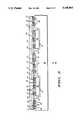
- the module substrate 19is illustrated in FIG. 3.
- the multi-chip module in this disclosurecan use a variety of module substrates 19 that span a range of performance and cost.
- Some examples of a module substrate materialare monolithic silicon with etched cavities, a composite of silicon and thermally conductive ceramic (aluminum nitride for example), monolithic aluminum nitride with molded/machined cavities, a composite of aluminum and aluminum nitride with machined cavity, and a multilayer fine-pitch organic board with conductive metal inserts for thermal vias.
- Interconnect on the substrates for the first four examplescould be built with multiple layers of conductive materials (Al,Cu), etched to form interconnect patterns and isolated from each other by dielectric layers such as polyimide.
- Each type of module substrate materialmay have a specific benefit for a multi-chip module application, all are directly applicable to the described invention.
- FIG. 3illustrates a plurality of composite structures 18 which are interconnected on a module substrate 19.
- Contact points 13 on bridge chip 12align with contact points 21 of module substrate 19.
- Module substrate 19has etched cavities 23 to accommodate integrated circuit 10 of composite structure 18.
- a conductive die attach material 24is placed in the bottom of the cavities 23.
- Contact points 13 on bridge chip 12are aligned with module substrate contact points 21 and merged until solder bumps 17 touch module substrate contact points 21.
- Conductive die attach material 24conforms to height variations due to varying cavity depths, integrated circuit thickness, and solder bump size.
- Conductive die attach material 24bonds integrated circuit 10 of composite structure 18 to module substrate 19.
- Conductive die attach material 24also forms a thermal pathway from integrated circuit 10 to module substrate 19.
- the conductive die attach material 24can be composed of an organic/inorganic material appropriate for the module application.
- Module substrate 19acts as a heat sink.
- a second thermal cycleis run which melts solder bumps 17 and connects composite structure contact points 13 to module substrate contact points 21.
- Solder bump material 17 used in the second thermal cycleshall have a lower melting point than the solder material in the first thermal cycle.
- the solder bonds formed in the first thermal cyclewill be unaffected by the second thermal cycle.
- Module substrate 19has interconnects 22 for interconnecting module substrate contact points 21 wherein interconnects 22 comprise metal lines.
- Multi-chip module 26can be tested through contact points on module substrate 19. By exhaustively testing the individual composite structures 18, testing of multi-chip module 26 need not be as comprehensive. The test can be limited to checking the interconnection of the composite structures 18 and a minimized functional test of multi-chip module 26. Prior methods required extensive testing of the multi-chip module due to limited burn-in/test capability on the individual integrated circuits. Low first pass yields on the assembled multi-chip modules adds cost, increases testing, and forces manufacturers to consider repair on the non-functional multi-chip modules.
- a multi-chip modulewhich addresses many of the limitations of current module approaches has been described.
- the novel designemploys bridge chip 12 which connects integrated circuit 10 to module substrate 19.
- Integrated circuit 10is attached to the bridge chip 12 which can be handled and tested as an individual unit prior to mounting on module substrate 19.
- a plurality of composite structures 18 of integrated circuit 10 and bridge chip 12are placed on module substrate 19 in such a way that each integrated circuit 10 has a thermal pathway to the module substrate 19.
- individual diecan be handled, comprehensive testing can be performed on the die, solder bumping can be localized to the bridge chip, the substrate is used as a heat sink, and final module testing can be reduced.
Landscapes
- Engineering & Computer Science (AREA)
- Microelectronics & Electronic Packaging (AREA)
- Computer Hardware Design (AREA)
- Physics & Mathematics (AREA)
- General Physics & Mathematics (AREA)
- Power Engineering (AREA)
- General Engineering & Computer Science (AREA)
- Condensed Matter Physics & Semiconductors (AREA)
- Environmental & Geological Engineering (AREA)
- Manufacturing & Machinery (AREA)
- Testing Of Individual Semiconductor Devices (AREA)
- Tests Of Electronic Circuits (AREA)
Abstract
Description
Claims (15)
Priority Applications (1)
| Application Number | Priority Date | Filing Date | Title |
|---|---|---|---|
| US07/795,440US5198963A (en) | 1991-11-21 | 1991-11-21 | Multiple integrated circuit module which simplifies handling and testing |
Applications Claiming Priority (1)
| Application Number | Priority Date | Filing Date | Title |
|---|---|---|---|
| US07/795,440US5198963A (en) | 1991-11-21 | 1991-11-21 | Multiple integrated circuit module which simplifies handling and testing |
Publications (1)
| Publication Number | Publication Date |
|---|---|
| US5198963Atrue US5198963A (en) | 1993-03-30 |
Family
ID=25165516
Family Applications (1)
| Application Number | Title | Priority Date | Filing Date |
|---|---|---|---|
| US07/795,440Expired - LifetimeUS5198963A (en) | 1991-11-21 | 1991-11-21 | Multiple integrated circuit module which simplifies handling and testing |
Country Status (1)
| Country | Link |
|---|---|
| US (1) | US5198963A (en) |
Cited By (92)
| Publication number | Priority date | Publication date | Assignee | Title |
|---|---|---|---|---|
| US5438224A (en)* | 1992-04-23 | 1995-08-01 | Motorola, Inc. | Integrated circuit package having a face-to-face IC chip arrangement |
| US5473192A (en)* | 1993-05-04 | 1995-12-05 | Motorola, Inc. | Unitary silicon die module |
| US5563445A (en)* | 1993-04-08 | 1996-10-08 | Seiko Epson Corporation | Semiconductor device |
| US5594276A (en)* | 1992-03-03 | 1997-01-14 | Sgs-Thomson Microelectronics, S.A. | Semiconductor device package with shaped parts for direct coupling to standard connectors |
| US5639683A (en)* | 1994-12-01 | 1997-06-17 | Motorola, Inc. | Structure and method for intergrating microwave components on a substrate |
| US5661343A (en)* | 1994-03-16 | 1997-08-26 | Hitachi, Ltd. | Power hybrid integrated circuit apparatus |
| US5719748A (en)* | 1995-06-28 | 1998-02-17 | Honeywell Inc. | Semiconductor package with a bridge for chip area connection |
| US5795818A (en)* | 1996-12-06 | 1998-08-18 | Amkor Technology, Inc. | Integrated circuit chip to substrate interconnection and method |
| US5815427A (en)* | 1997-04-02 | 1998-09-29 | Micron Technology, Inc. | Modular memory circuit and method for forming same |
| US5821762A (en)* | 1994-02-28 | 1998-10-13 | Mitsubishi Denki Kabushiki Kaisha | Semiconductor device, production method therefor, method for testing semiconductor elements, test substrate for the method and method for producing the test substrate |
| US5825092A (en)* | 1996-05-20 | 1998-10-20 | Harris Corporation | Integrated circuit with an air bridge having a lid |
| US5869894A (en)* | 1997-07-18 | 1999-02-09 | Lucent Technologies Inc. | RF IC package |
| US6075711A (en)* | 1996-10-21 | 2000-06-13 | Alpine Microsystems, Inc. | System and method for routing connections of integrated circuits |
| EP0908951A3 (en)* | 1997-10-08 | 2000-07-19 | Lucent Technologies Inc. | Improved air isolated crossovers |
| US6111756A (en)* | 1998-09-11 | 2000-08-29 | Fujitsu Limited | Universal multichip interconnect systems |
| US6121682A (en)* | 1998-12-26 | 2000-09-19 | Hyundai Electronics Industries Co., Ltd. | Multi-chip package |
| US6166444A (en)* | 1999-06-21 | 2000-12-26 | United Microelectronics Corp. | Cascade-type chip module |
| US6215193B1 (en)* | 1999-04-21 | 2001-04-10 | Advanced Semiconductor Engineering, Inc. | Multichip modules and manufacturing method therefor |
| US6222212B1 (en)* | 1994-01-27 | 2001-04-24 | Integrated Device Technology, Inc. | Semiconductor device having programmable interconnect layers |
| US6297551B1 (en)* | 1999-09-22 | 2001-10-02 | Agere Systems Guardian Corp. | Integrated circuit packages with improved EMI characteristics |
| WO2001024259A3 (en)* | 1999-09-30 | 2001-11-29 | Alpha Ind Inc | Semiconductor packaging |
| US6327408B1 (en) | 1999-10-19 | 2001-12-04 | Corning Incorporated | Electrical interconnection of planar lightwave circuits |
| US6330164B1 (en)* | 1985-10-18 | 2001-12-11 | Formfactor, Inc. | Interconnect assemblies and methods including ancillary electronic component connected in immediate proximity of semiconductor device |
| US6369444B1 (en)* | 1998-05-19 | 2002-04-09 | Agere Systems Guardian Corp. | Packaging silicon on silicon multichip modules |
| US6407566B1 (en) | 2000-04-06 | 2002-06-18 | Micron Technology, Inc. | Test module for multi-chip module simulation testing of integrated circuit packages |
| US6455945B1 (en)* | 1994-01-28 | 2002-09-24 | Fujitsu, Limited | Semiconductor device having a fragment of a connection part provided on at least one lateral edge for mechanically connecting to adjacent semiconductor chips |
| US6464513B1 (en) | 2000-01-05 | 2002-10-15 | Micron Technology, Inc. | Adapter for non-permanently connecting integrated circuit devices to multi-chip modules and method of using same |
| US6476499B1 (en)* | 1999-02-08 | 2002-11-05 | Rohm Co., | Semiconductor chip, chip-on-chip structure device and assembling method thereof |
| US6489669B2 (en)* | 2000-09-11 | 2002-12-03 | Rohm Co., Ltd. | Integrated circuit device |
| US20030008424A1 (en)* | 2001-07-09 | 2003-01-09 | Matsushita Electric Industrial Co., Ltd. | Multichip module and method for testing connection of the module |
| US20030040139A1 (en)* | 2001-08-21 | 2003-02-27 | Canella Robert L. | Spring contact for establishing non-permanent electrical connection between an integrated circuit device lead element and a substrate, apparatus including same and method of use |
| US20030042595A1 (en)* | 2001-08-29 | 2003-03-06 | Canella Robert L. | Substrate with contact array and substrate assemblies |
| US6563205B1 (en)* | 1995-08-16 | 2003-05-13 | Micron Technology, Inc. | Angularly offset and recessed stacked die multichip device and method of manufacture |
| US20030122223A1 (en)* | 1998-04-02 | 2003-07-03 | Akio Nakamura | Semiconductor device in a recess of a semiconductor plate |
| US20030127715A1 (en)* | 2002-01-07 | 2003-07-10 | Cheng-Yi Liu | Thinned die integrated circuit package |
| US6646342B2 (en) | 2001-03-14 | 2003-11-11 | Matsushita Electric Industrial Co., Ltd. | Semiconductor chip and multi-chip module |
| US6664628B2 (en) | 1998-07-13 | 2003-12-16 | Formfactor, Inc. | Electronic component overlapping dice of unsingulated semiconductor wafer |
| US20040012094A1 (en)* | 2002-07-18 | 2004-01-22 | Harper Timothy V. | Flip-chip integrated circuit package and method of assembly |
| US20040012941A1 (en)* | 2001-09-30 | 2004-01-22 | Intel Corporation | Low profile stacked multi-chip package and method of forming same |
| US20040212067A1 (en)* | 2003-04-25 | 2004-10-28 | Advanced Semiconductor Engineering, Inc. | Multi-chips stacked package |
| US20040217459A1 (en)* | 2001-03-30 | 2004-11-04 | Fee Setho Sing | Ball grid array interposer, packages and methods |
| US6825055B2 (en)* | 2000-08-29 | 2004-11-30 | Matsushita Electric Industrial Co., Ltd. | Method for assembling integral type electronic component and integral type electronic component |
| US20040238857A1 (en)* | 2001-08-28 | 2004-12-02 | Tessera, Inc. | High frequency chip packages with connecting elements |
| US20050046001A1 (en)* | 2001-08-28 | 2005-03-03 | Tessera, Inc | High-frequency chip packages |
| US6867499B1 (en) | 1999-09-30 | 2005-03-15 | Skyworks Solutions, Inc. | Semiconductor packaging |
| US20050067681A1 (en)* | 2003-09-26 | 2005-03-31 | Tessera, Inc. | Package having integral lens and wafer-scale fabrication method therefor |
| US20050082654A1 (en)* | 2003-09-26 | 2005-04-21 | Tessera, Inc. | Structure and self-locating method of making capped chips |
| US6884657B1 (en) | 1995-08-16 | 2005-04-26 | Micron Technology, Inc. | Angularly offset stacked die multichip device and method of manufacture |
| US20050136640A1 (en)* | 2002-01-07 | 2005-06-23 | Chuan Hu | Die exhibiting an effective coefficient of thermal expansion equivalent to a substrate mounted thereon, and processes of making same |
| US20050139984A1 (en)* | 2003-12-19 | 2005-06-30 | Tessera, Inc. | Package element and packaged chip having severable electrically conductive ties |
| US20050145994A1 (en)* | 2004-01-06 | 2005-07-07 | International Business Machines Corporation | Compliant passivated edge seal for low-k interconnect structures |
| US20050189622A1 (en)* | 2004-03-01 | 2005-09-01 | Tessera, Inc. | Packaged acoustic and electromagnetic transducer chips |
| US20050218518A1 (en)* | 2002-01-07 | 2005-10-06 | Tongbi Jiang | Semiconductor device assemblies and packages including multiple semiconductor device components |
| US20060027913A1 (en)* | 2003-07-02 | 2006-02-09 | Matthias Lungwitz | Shielding for emi-sensitive electronic components and or circuits of electronic devices |
| US20070109756A1 (en)* | 2005-02-10 | 2007-05-17 | Stats Chippac Ltd. | Stacked integrated circuits package system |
| US20070138647A1 (en)* | 2005-12-21 | 2007-06-21 | Qing Zhou | Integrated circuit package to provide high-bandwidth communication among multiple dice |
| US20070138498A1 (en)* | 2003-07-03 | 2007-06-21 | Tessera Technologies Hungary Kft. | Methods and apparatus for packaging integrated circuit devices |
| US20070145564A1 (en)* | 2005-03-22 | 2007-06-28 | Tessera, Inc. | Sequential fabrication of vertical conductive interconnects in capped chips |
| US20070190747A1 (en)* | 2006-01-23 | 2007-08-16 | Tessera Technologies Hungary Kft. | Wafer level packaging to lidded chips |
| US20070190691A1 (en)* | 2006-01-23 | 2007-08-16 | Tessera Technologies Hungary Kft. | Wafer level chip packaging |
| US7265440B2 (en) | 2003-06-16 | 2007-09-04 | Tessera Technologies Hungary Kft. | Methods and apparatus for packaging integrated circuit devices |
| US20080002460A1 (en)* | 2006-03-01 | 2008-01-03 | Tessera, Inc. | Structure and method of making lidded chips |
| US20110068737A1 (en)* | 2009-09-24 | 2011-03-24 | Lear Corporation | System and method for reduced thermal resistance between a power electronics printed circuit board and a base plate |
| US20110215472A1 (en)* | 2008-06-30 | 2011-09-08 | Qualcomm Incorporated | Through Silicon via Bridge Interconnect |
| US20110285006A1 (en)* | 2010-05-19 | 2011-11-24 | Chao-Fu Weng | Semiconductor Package and Method for Making the Same |
| CN102947926A (en)* | 2010-06-17 | 2013-02-27 | 浜松光子学株式会社 | Semiconductor integrated circuit device inspection method and semiconductor integrated circuit device |
| US8558395B2 (en) | 2012-02-21 | 2013-10-15 | Broadcom Corporation | Organic interface substrate having interposer with through-semiconductor vias |
| US8587132B2 (en)* | 2012-02-21 | 2013-11-19 | Broadcom Corporation | Semiconductor package including an organic substrate and interposer having through-semiconductor vias |
| US8592259B2 (en) | 2011-11-29 | 2013-11-26 | Broadcom Corporation | Method of fabricating a wafer level semiconductor package having a pre-formed dielectric layer |
| US8604605B2 (en) | 2007-01-05 | 2013-12-10 | Invensas Corp. | Microelectronic assembly with multi-layer support structure |
| US20130341076A1 (en)* | 2008-03-28 | 2013-12-26 | Aleksandar Aleksov | Package substrate and die spacer layers having a ceramic backbone |
| US20140035114A1 (en)* | 2012-01-19 | 2014-02-06 | Semiconductor Components Industries, Llc | Semiconductor package structure and method |
| US8680670B2 (en) | 2010-10-22 | 2014-03-25 | International Business Machines Corporation | Multi-chip module system with removable socketed modules |
| US8749072B2 (en) | 2012-02-24 | 2014-06-10 | Broadcom Corporation | Semiconductor package with integrated selectively conductive film interposer |
| US20140264791A1 (en)* | 2013-03-14 | 2014-09-18 | Mathew J. Manusharow | Direct external interconnect for embedded interconnect bridge package |
| US8872321B2 (en) | 2012-02-24 | 2014-10-28 | Broadcom Corporation | Semiconductor packages with integrated heat spreaders |
| US8957516B2 (en) | 2012-01-24 | 2015-02-17 | Broadcom Corporation | Low cost and high performance flip chip package |
| US9059179B2 (en) | 2011-12-28 | 2015-06-16 | Broadcom Corporation | Semiconductor package with a bridge interposer |
| US20150228583A1 (en)* | 2013-06-28 | 2015-08-13 | Omkar G. Karhade | Reliable microstrip routing for electronics components |
| US20150380369A1 (en)* | 2013-09-30 | 2015-12-31 | Nantong Fujitsu Microelectronics Co., Ltd | Wafer packaging structure and packaging method |
| US9275976B2 (en) | 2012-02-24 | 2016-03-01 | Broadcom Corporation | System-in-package with integrated socket |
| US9293393B2 (en) | 2011-12-14 | 2016-03-22 | Broadcom Corporation | Stacked packaging using reconstituted wafers |
| US9548251B2 (en) | 2012-01-12 | 2017-01-17 | Broadcom Corporation | Semiconductor interposer having a cavity for intra-interposer die |
| US20170125349A1 (en)* | 2012-12-20 | 2017-05-04 | Intel Corporation | High density organic bridge device and method |
| US10224272B2 (en)* | 2016-08-05 | 2019-03-05 | Samsung Electronics Co., Ltd. | Semiconductor package including a rewiring layer with an embedded chip |
| US20200075493A1 (en)* | 2009-06-24 | 2020-03-05 | Intel Corporation | Multi-chip package and method of providing die-to-die interconnects in same |
| US10957650B2 (en) | 2019-08-21 | 2021-03-23 | International Business Machines Corporation | Bridge support structure |
| US11114418B2 (en)* | 2016-11-01 | 2021-09-07 | Fujitsu Limited | Electronic device, method of manufacturing electronic device, and electronic apparatus |
| CN113777465A (en)* | 2020-06-09 | 2021-12-10 | 台湾爱司帝科技股份有限公司 | Chip detection method, chip detection structure and chip bearing structure |
| US20220199539A1 (en)* | 2020-12-18 | 2022-06-23 | Intel Corporation | Microelectronic structures including bridges |
| US20230130944A1 (en)* | 2012-09-28 | 2023-04-27 | Intel Corporation | Localized high density substrate routing |
| US20230137977A1 (en)* | 2021-10-29 | 2023-05-04 | Nxp B.V. | Stacking a semiconductor die and chip-scale-package unit |
Citations (3)
| Publication number | Priority date | Publication date | Assignee | Title |
|---|---|---|---|---|
| US3436604A (en)* | 1966-04-25 | 1969-04-01 | Texas Instruments Inc | Complex integrated circuit array and method for fabricating same |
| US4744008A (en)* | 1986-11-18 | 1988-05-10 | International Business Machines Corporation | Flexible film chip carrier with decoupling capacitors |
| US5049978A (en)* | 1990-09-10 | 1991-09-17 | General Electric Company | Conductively enclosed hybrid integrated circuit assembly using a silicon substrate |
- 1991
- 1991-11-21USUS07/795,440patent/US5198963A/ennot_activeExpired - Lifetime
Patent Citations (3)
| Publication number | Priority date | Publication date | Assignee | Title |
|---|---|---|---|---|
| US3436604A (en)* | 1966-04-25 | 1969-04-01 | Texas Instruments Inc | Complex integrated circuit array and method for fabricating same |
| US4744008A (en)* | 1986-11-18 | 1988-05-10 | International Business Machines Corporation | Flexible film chip carrier with decoupling capacitors |
| US5049978A (en)* | 1990-09-10 | 1991-09-17 | General Electric Company | Conductively enclosed hybrid integrated circuit assembly using a silicon substrate |
Non-Patent Citations (2)
| Title |
|---|
| Larnerd "IC Pakage Assembly", IBM Tech. Disclosure Bulletin, vol. 20, No. 12, May 1978 pp. 5142-5143. |
| Larnerd IC Pakage Assembly , IBM Tech. Disclosure Bulletin, vol. 20, No. 12, May 1978 pp. 5142 5143.* |
Cited By (176)
| Publication number | Priority date | Publication date | Assignee | Title |
|---|---|---|---|---|
| US6330164B1 (en)* | 1985-10-18 | 2001-12-11 | Formfactor, Inc. | Interconnect assemblies and methods including ancillary electronic component connected in immediate proximity of semiconductor device |
| US5594276A (en)* | 1992-03-03 | 1997-01-14 | Sgs-Thomson Microelectronics, S.A. | Semiconductor device package with shaped parts for direct coupling to standard connectors |
| US5438224A (en)* | 1992-04-23 | 1995-08-01 | Motorola, Inc. | Integrated circuit package having a face-to-face IC chip arrangement |
| US5563445A (en)* | 1993-04-08 | 1996-10-08 | Seiko Epson Corporation | Semiconductor device |
| US5473192A (en)* | 1993-05-04 | 1995-12-05 | Motorola, Inc. | Unitary silicon die module |
| US6222212B1 (en)* | 1994-01-27 | 2001-04-24 | Integrated Device Technology, Inc. | Semiconductor device having programmable interconnect layers |
| US6455945B1 (en)* | 1994-01-28 | 2002-09-24 | Fujitsu, Limited | Semiconductor device having a fragment of a connection part provided on at least one lateral edge for mechanically connecting to adjacent semiconductor chips |
| US5821762A (en)* | 1994-02-28 | 1998-10-13 | Mitsubishi Denki Kabushiki Kaisha | Semiconductor device, production method therefor, method for testing semiconductor elements, test substrate for the method and method for producing the test substrate |
| JP3288840B2 (en) | 1994-02-28 | 2002-06-04 | 三菱電機株式会社 | Semiconductor device and manufacturing method thereof |
| US5661343A (en)* | 1994-03-16 | 1997-08-26 | Hitachi, Ltd. | Power hybrid integrated circuit apparatus |
| US5639683A (en)* | 1994-12-01 | 1997-06-17 | Motorola, Inc. | Structure and method for intergrating microwave components on a substrate |
| US5719748A (en)* | 1995-06-28 | 1998-02-17 | Honeywell Inc. | Semiconductor package with a bridge for chip area connection |
| US6563205B1 (en)* | 1995-08-16 | 2003-05-13 | Micron Technology, Inc. | Angularly offset and recessed stacked die multichip device and method of manufacture |
| US6884657B1 (en) | 1995-08-16 | 2005-04-26 | Micron Technology, Inc. | Angularly offset stacked die multichip device and method of manufacture |
| US5825092A (en)* | 1996-05-20 | 1998-10-20 | Harris Corporation | Integrated circuit with an air bridge having a lid |
| US6075711A (en)* | 1996-10-21 | 2000-06-13 | Alpine Microsystems, Inc. | System and method for routing connections of integrated circuits |
| US6163463A (en)* | 1996-12-06 | 2000-12-19 | Amkor Technology, Inc. | Integrated circuit chip to substrate interconnection |
| US5795818A (en)* | 1996-12-06 | 1998-08-18 | Amkor Technology, Inc. | Integrated circuit chip to substrate interconnection and method |
| US5815427A (en)* | 1997-04-02 | 1998-09-29 | Micron Technology, Inc. | Modular memory circuit and method for forming same |
| EP0892434A3 (en)* | 1997-07-18 | 1999-09-01 | Lucent Technologies Inc. | RF IC package |
| US5869894A (en)* | 1997-07-18 | 1999-02-09 | Lucent Technologies Inc. | RF IC package |
| JP2007274004A (en)* | 1997-10-08 | 2007-10-18 | Lucent Technol Inc | Integrated circuit device |
| EP0908951A3 (en)* | 1997-10-08 | 2000-07-19 | Lucent Technologies Inc. | Improved air isolated crossovers |
| US7183132B2 (en)* | 1998-04-02 | 2007-02-27 | Oki Electric Industry Co., Ltd. | Semiconductor device in a recess of a semiconductor plate |
| US20030122223A1 (en)* | 1998-04-02 | 2003-07-03 | Akio Nakamura | Semiconductor device in a recess of a semiconductor plate |
| US6369444B1 (en)* | 1998-05-19 | 2002-04-09 | Agere Systems Guardian Corp. | Packaging silicon on silicon multichip modules |
| US6664628B2 (en) | 1998-07-13 | 2003-12-16 | Formfactor, Inc. | Electronic component overlapping dice of unsingulated semiconductor wafer |
| US6111756A (en)* | 1998-09-11 | 2000-08-29 | Fujitsu Limited | Universal multichip interconnect systems |
| US6121682A (en)* | 1998-12-26 | 2000-09-19 | Hyundai Electronics Industries Co., Ltd. | Multi-chip package |
| US6869829B2 (en) | 1999-02-08 | 2005-03-22 | Rohm Co., Ltd. | Semiconductor chip, chip-on-chip structure device, and assembling method thereof |
| US6476499B1 (en)* | 1999-02-08 | 2002-11-05 | Rohm Co., | Semiconductor chip, chip-on-chip structure device and assembling method thereof |
| US6215193B1 (en)* | 1999-04-21 | 2001-04-10 | Advanced Semiconductor Engineering, Inc. | Multichip modules and manufacturing method therefor |
| US6166444A (en)* | 1999-06-21 | 2000-12-26 | United Microelectronics Corp. | Cascade-type chip module |
| US6297551B1 (en)* | 1999-09-22 | 2001-10-02 | Agere Systems Guardian Corp. | Integrated circuit packages with improved EMI characteristics |
| WO2001024259A3 (en)* | 1999-09-30 | 2001-11-29 | Alpha Ind Inc | Semiconductor packaging |
| US20050124232A1 (en)* | 1999-09-30 | 2005-06-09 | Behnam Tabrizi | Semiconductor packaging |
| US6867499B1 (en) | 1999-09-30 | 2005-03-15 | Skyworks Solutions, Inc. | Semiconductor packaging |
| US7192810B2 (en) | 1999-09-30 | 2007-03-20 | Skyworks Solutions, Inc. | Semiconductor packaging |
| US6327408B1 (en) | 1999-10-19 | 2001-12-04 | Corning Incorporated | Electrical interconnection of planar lightwave circuits |
| US20050082661A1 (en)* | 2000-01-05 | 2005-04-21 | Saeed Momempour | Adapter for non-permanently connecting integrated circuit devices to multi-chip modules and method of using same |
| US6464513B1 (en) | 2000-01-05 | 2002-10-15 | Micron Technology, Inc. | Adapter for non-permanently connecting integrated circuit devices to multi-chip modules and method of using same |
| US7326066B2 (en) | 2000-01-05 | 2008-02-05 | Micron Technology, Inc. | Adapter for non-permanently connecting integrated circuit devices to multi-chip modules and method of using same |
| US20020196598A1 (en)* | 2000-01-05 | 2002-12-26 | Saeed Momenpour | Adapter for non-permanently connecting integrated circuit devices to multi-chip modules and method of using same |
| US6843661B2 (en) | 2000-01-05 | 2005-01-18 | Micron Technology, Inc. | Adapter for non-permanently connecting integrated circuit devices to multi-chip modules and method of using same |
| US6407566B1 (en) | 2000-04-06 | 2002-06-18 | Micron Technology, Inc. | Test module for multi-chip module simulation testing of integrated circuit packages |
| US6825055B2 (en)* | 2000-08-29 | 2004-11-30 | Matsushita Electric Industrial Co., Ltd. | Method for assembling integral type electronic component and integral type electronic component |
| US20050001315A1 (en)* | 2000-08-29 | 2005-01-06 | Kazushi Higashi | Method for assembling integral type electronic device, and integral type electronic device |
| US6489669B2 (en)* | 2000-09-11 | 2002-12-03 | Rohm Co., Ltd. | Integrated circuit device |
| US6646342B2 (en) | 2001-03-14 | 2003-11-11 | Matsushita Electric Industrial Co., Ltd. | Semiconductor chip and multi-chip module |
| US20040217459A1 (en)* | 2001-03-30 | 2004-11-04 | Fee Setho Sing | Ball grid array interposer, packages and methods |
| US7274095B2 (en) | 2001-03-30 | 2007-09-25 | Micron Technology, Inc. | Interposers with receptacles for receiving semiconductor devices and assemblies and packages including such interposers |
| US20060194373A1 (en)* | 2001-03-30 | 2006-08-31 | Fee Setho S | Methods for assembling semiconductor devices and interposers |
| US7528007B2 (en) | 2001-03-30 | 2009-05-05 | Micron Technology, Inc. | Methods for assembling semiconductor devices and interposers |
| US6833626B2 (en) | 2001-07-09 | 2004-12-21 | Matsushita Electric Industrial. Co., Ltd. | Multichip module structure |
| US20030008424A1 (en)* | 2001-07-09 | 2003-01-09 | Matsushita Electric Industrial Co., Ltd. | Multichip module and method for testing connection of the module |
| US7192806B2 (en) | 2001-08-21 | 2007-03-20 | Micron Technology, Inc. | Method of establishing non-permanent electrical connection between an integrated circuit device lead element and a substrate |
| US20050070133A1 (en)* | 2001-08-21 | 2005-03-31 | Canella Robert L. | Device for establishing non-permanent electrical connection between an integrated circuit device lead element and a substrate |
| US20050073041A1 (en)* | 2001-08-21 | 2005-04-07 | Canella Robert L. | Device for establishing non-permanent electrical connection between an integrated circuit device lead element and a substrate |
| US7279788B2 (en) | 2001-08-21 | 2007-10-09 | Micron Technology, Inc. | Device for establishing non-permanent electrical connection between an integrated circuit device lead element and a substrate |
| US20030040139A1 (en)* | 2001-08-21 | 2003-02-27 | Canella Robert L. | Spring contact for establishing non-permanent electrical connection between an integrated circuit device lead element and a substrate, apparatus including same and method of use |
| US7045889B2 (en) | 2001-08-21 | 2006-05-16 | Micron Technology, Inc. | Device for establishing non-permanent electrical connection between an integrated circuit device lead element and a substrate |
| US20050067687A1 (en)* | 2001-08-21 | 2005-03-31 | Canella Robert L. | Device for establishing non-permanent electrical connection between an integrated circuit device lead element and a substrate |
| US7094065B2 (en) | 2001-08-21 | 2006-08-22 | Micron Technology, Inc. | Device for establishing non-permanent electrical connection between an integrated circuit device lead element and a substrate |
| US20050046001A1 (en)* | 2001-08-28 | 2005-03-03 | Tessera, Inc | High-frequency chip packages |
| US20060113645A1 (en)* | 2001-08-28 | 2006-06-01 | Tessera, Inc. | Microelectronic assemblies incorporating inductors |
| US7566955B2 (en) | 2001-08-28 | 2009-07-28 | Tessera, Inc. | High-frequency chip packages |
| US7176506B2 (en)* | 2001-08-28 | 2007-02-13 | Tessera, Inc. | High frequency chip packages with connecting elements |
| US20040238857A1 (en)* | 2001-08-28 | 2004-12-02 | Tessera, Inc. | High frequency chip packages with connecting elements |
| US20030042595A1 (en)* | 2001-08-29 | 2003-03-06 | Canella Robert L. | Substrate with contact array and substrate assemblies |
| US7120999B2 (en) | 2001-08-29 | 2006-10-17 | Micron Technology, Inc. | Methods of forming a contact array in situ on a substrate |
| US20040058470A1 (en)* | 2001-08-29 | 2004-03-25 | Canella Robert L. | Methods of forming a contact array in situ on a substrate and resulting substrate assemblies |
| US7049693B2 (en) | 2001-08-29 | 2006-05-23 | Micron Technology, Inc. | Electrical contact array for substrate assemblies |
| US20040012941A1 (en)* | 2001-09-30 | 2004-01-22 | Intel Corporation | Low profile stacked multi-chip package and method of forming same |
| US7009300B2 (en)* | 2001-09-30 | 2006-03-07 | Intel Corporation | Low profile stacked multi-chip package and method of forming same |
| US7420273B2 (en) | 2002-01-07 | 2008-09-02 | Intel Corporation | Thinned die integrated circuit package |
| US20050121778A1 (en)* | 2002-01-07 | 2005-06-09 | Intel Corporation | Thinned die integrated circuit package |
| US20050218518A1 (en)* | 2002-01-07 | 2005-10-06 | Tongbi Jiang | Semiconductor device assemblies and packages including multiple semiconductor device components |
| US6841413B2 (en)* | 2002-01-07 | 2005-01-11 | Intel Corporation | Thinned die integrated circuit package |
| US20080153209A1 (en)* | 2002-01-07 | 2008-06-26 | Intel Corporation | Thinned die integrated circuit package |
| US7888183B2 (en) | 2002-01-07 | 2011-02-15 | Intel Corporation | Thinned die integrated circuit package |
| US20050136640A1 (en)* | 2002-01-07 | 2005-06-23 | Chuan Hu | Die exhibiting an effective coefficient of thermal expansion equivalent to a substrate mounted thereon, and processes of making same |
| US20030127715A1 (en)* | 2002-01-07 | 2003-07-10 | Cheng-Yi Liu | Thinned die integrated circuit package |
| US7573136B2 (en)* | 2002-06-27 | 2009-08-11 | Micron Technology, Inc. | Semiconductor device assemblies and packages including multiple semiconductor device components |
| US20040012094A1 (en)* | 2002-07-18 | 2004-01-22 | Harper Timothy V. | Flip-chip integrated circuit package and method of assembly |
| US20040212067A1 (en)* | 2003-04-25 | 2004-10-28 | Advanced Semiconductor Engineering, Inc. | Multi-chips stacked package |
| US7642629B2 (en) | 2003-06-16 | 2010-01-05 | Tessera Technologies Hungary Kft. | Methods and apparatus for packaging integrated circuit devices |
| US7265440B2 (en) | 2003-06-16 | 2007-09-04 | Tessera Technologies Hungary Kft. | Methods and apparatus for packaging integrated circuit devices |
| US20060027913A1 (en)* | 2003-07-02 | 2006-02-09 | Matthias Lungwitz | Shielding for emi-sensitive electronic components and or circuits of electronic devices |
| US7269032B2 (en)* | 2003-07-02 | 2007-09-11 | Siemens Aktiengesellschaft | Shielding for EMI-sensitive electronic components and or circuits of electronic devices |
| US7495341B2 (en) | 2003-07-03 | 2009-02-24 | Tessera Technologies Hungary Kft. | Methods and apparatus for packaging integrated circuit devices |
| US7479398B2 (en) | 2003-07-03 | 2009-01-20 | Tessera Technologies Hungary Kft. | Methods and apparatus for packaging integrated circuit devices |
| US20070138498A1 (en)* | 2003-07-03 | 2007-06-21 | Tessera Technologies Hungary Kft. | Methods and apparatus for packaging integrated circuit devices |
| US7224056B2 (en) | 2003-09-26 | 2007-05-29 | Tessera, Inc. | Back-face and edge interconnects for lidded package |
| US20050067681A1 (en)* | 2003-09-26 | 2005-03-31 | Tessera, Inc. | Package having integral lens and wafer-scale fabrication method therefor |
| US20050082654A1 (en)* | 2003-09-26 | 2005-04-21 | Tessera, Inc. | Structure and self-locating method of making capped chips |
| US20050087861A1 (en)* | 2003-09-26 | 2005-04-28 | Tessera, Inc. | Back-face and edge interconnects for lidded package |
| US20050095835A1 (en)* | 2003-09-26 | 2005-05-05 | Tessera, Inc. | Structure and method of making capped chips having vertical interconnects |
| US20080032457A1 (en)* | 2003-09-26 | 2008-02-07 | Tessera, Inc. | Structure and method of making sealed capped chips |
| US20070096312A1 (en)* | 2003-09-26 | 2007-05-03 | Tessera, Inc. | Structure and self-locating method of making capped chips |
| US20070096311A1 (en)* | 2003-09-26 | 2007-05-03 | Tessera, Inc. | Structure and method of making capped chips having vertical interconnects |
| US20050139984A1 (en)* | 2003-12-19 | 2005-06-30 | Tessera, Inc. | Package element and packaged chip having severable electrically conductive ties |
| US20060281224A1 (en)* | 2004-01-06 | 2006-12-14 | International Business Machines Corporation | Compliant passivated edge seal for low-k interconnect structures |
| US7273770B2 (en) | 2004-01-06 | 2007-09-25 | International Business Machines Corporation | Compliant passivated edge seal for low-k interconnect structures |
| US7098544B2 (en)* | 2004-01-06 | 2006-08-29 | International Business Machines Corporation | Edge seal for integrated circuit chips |
| US20050145994A1 (en)* | 2004-01-06 | 2005-07-07 | International Business Machines Corporation | Compliant passivated edge seal for low-k interconnect structures |
| US20050189635A1 (en)* | 2004-03-01 | 2005-09-01 | Tessera, Inc. | Packaged acoustic and electromagnetic transducer chips |
| US20050189622A1 (en)* | 2004-03-01 | 2005-09-01 | Tessera, Inc. | Packaged acoustic and electromagnetic transducer chips |
| US20070109756A1 (en)* | 2005-02-10 | 2007-05-17 | Stats Chippac Ltd. | Stacked integrated circuits package system |
| US8143095B2 (en) | 2005-03-22 | 2012-03-27 | Tessera, Inc. | Sequential fabrication of vertical conductive interconnects in capped chips |
| US20070145564A1 (en)* | 2005-03-22 | 2007-06-28 | Tessera, Inc. | Sequential fabrication of vertical conductive interconnects in capped chips |
| US7348678B2 (en)* | 2005-12-21 | 2008-03-25 | Intel Corporation | Integrated circuit package to provide high-bandwidth communication among multiple dice |
| US20070138647A1 (en)* | 2005-12-21 | 2007-06-21 | Qing Zhou | Integrated circuit package to provide high-bandwidth communication among multiple dice |
| US20070190691A1 (en)* | 2006-01-23 | 2007-08-16 | Tessera Technologies Hungary Kft. | Wafer level chip packaging |
| US7936062B2 (en) | 2006-01-23 | 2011-05-03 | Tessera Technologies Ireland Limited | Wafer level chip packaging |
| US20070190747A1 (en)* | 2006-01-23 | 2007-08-16 | Tessera Technologies Hungary Kft. | Wafer level packaging to lidded chips |
| US20080029879A1 (en)* | 2006-03-01 | 2008-02-07 | Tessera, Inc. | Structure and method of making lidded chips |
| US20080002460A1 (en)* | 2006-03-01 | 2008-01-03 | Tessera, Inc. | Structure and method of making lidded chips |
| US8604605B2 (en) | 2007-01-05 | 2013-12-10 | Invensas Corp. | Microelectronic assembly with multi-layer support structure |
| US9548145B2 (en) | 2007-01-05 | 2017-01-17 | Invensas Corporation | Microelectronic assembly with multi-layer support structure |
| US9258880B2 (en)* | 2008-03-28 | 2016-02-09 | Intel Corporation | Package substrate and die spacer layers having a ceramic backbone |
| US20130341076A1 (en)* | 2008-03-28 | 2013-12-26 | Aleksandar Aleksov | Package substrate and die spacer layers having a ceramic backbone |
| US20110215472A1 (en)* | 2008-06-30 | 2011-09-08 | Qualcomm Incorporated | Through Silicon via Bridge Interconnect |
| US20210134726A1 (en)* | 2009-06-24 | 2021-05-06 | Intel Corporation | Multi-chip package and method of providing die-to-die interconnects in same |
| US10923429B2 (en)* | 2009-06-24 | 2021-02-16 | Intel Corporation | Multi-chip package and method of providing die-to-die interconnects in same |
| US12113026B2 (en)* | 2009-06-24 | 2024-10-08 | Intel Corporation | Multi-chip package and method of providing die-to-die interconnects in same |
| US20200075493A1 (en)* | 2009-06-24 | 2020-03-05 | Intel Corporation | Multi-chip package and method of providing die-to-die interconnects in same |
| US11876053B2 (en)* | 2009-06-24 | 2024-01-16 | Intel Corporation | Multi-chip package and method of providing die-to-die interconnects in same |
| US10763216B2 (en)* | 2009-06-24 | 2020-09-01 | Intel Corporation | Multi-chip package and method of providing die-to-die interconnects in same |
| US11824008B2 (en)* | 2009-06-24 | 2023-11-21 | Intel Corporation | Multi-chip package and method of providing die-to-die interconnects in same |
| US20240038671A1 (en)* | 2009-06-24 | 2024-02-01 | Intel Corporation | Multi-chip package and method of providing die-to-die interconnects in same |
| US20110068737A1 (en)* | 2009-09-24 | 2011-03-24 | Lear Corporation | System and method for reduced thermal resistance between a power electronics printed circuit board and a base plate |
| US8848375B2 (en)* | 2009-09-24 | 2014-09-30 | Lear Corporation | System and method for reduced thermal resistance between a power electronics printed circuit board and a base plate |
| US8288854B2 (en)* | 2010-05-19 | 2012-10-16 | Advanced Semiconductor Engineering, Inc. | Semiconductor package and method for making the same |
| US20110285006A1 (en)* | 2010-05-19 | 2011-11-24 | Chao-Fu Weng | Semiconductor Package and Method for Making the Same |
| CN102947926A (en)* | 2010-06-17 | 2013-02-27 | 浜松光子学株式会社 | Semiconductor integrated circuit device inspection method and semiconductor integrated circuit device |
| CN102947926B (en)* | 2010-06-17 | 2015-09-23 | 浜松光子学株式会社 | The inspection method of conductor integrated circuit device and conductor integrated circuit device |
| US8680670B2 (en) | 2010-10-22 | 2014-03-25 | International Business Machines Corporation | Multi-chip module system with removable socketed modules |
| US8592259B2 (en) | 2011-11-29 | 2013-11-26 | Broadcom Corporation | Method of fabricating a wafer level semiconductor package having a pre-formed dielectric layer |
| US9293393B2 (en) | 2011-12-14 | 2016-03-22 | Broadcom Corporation | Stacked packaging using reconstituted wafers |
| US9059179B2 (en) | 2011-12-28 | 2015-06-16 | Broadcom Corporation | Semiconductor package with a bridge interposer |
| US9431371B2 (en) | 2011-12-28 | 2016-08-30 | Broadcom Corporation | Semiconductor package with a bridge interposer |
| US9548251B2 (en) | 2012-01-12 | 2017-01-17 | Broadcom Corporation | Semiconductor interposer having a cavity for intra-interposer die |
| US20140035114A1 (en)* | 2012-01-19 | 2014-02-06 | Semiconductor Components Industries, Llc | Semiconductor package structure and method |
| US9799627B2 (en)* | 2012-01-19 | 2017-10-24 | Semiconductor Components Industries, Llc | Semiconductor package structure and method |
| US8957516B2 (en) | 2012-01-24 | 2015-02-17 | Broadcom Corporation | Low cost and high performance flip chip package |
| US8829655B2 (en) | 2012-02-21 | 2014-09-09 | Broadcom Corporation | Semiconductor package including a substrate and an interposer |
| US8829654B2 (en) | 2012-02-21 | 2014-09-09 | Broadcom Corporation | Semiconductor package with interposer |
| US8558395B2 (en) | 2012-02-21 | 2013-10-15 | Broadcom Corporation | Organic interface substrate having interposer with through-semiconductor vias |
| US8587132B2 (en)* | 2012-02-21 | 2013-11-19 | Broadcom Corporation | Semiconductor package including an organic substrate and interposer having through-semiconductor vias |
| US8664772B2 (en) | 2012-02-21 | 2014-03-04 | Broadcom Corporation | Interface substrate with interposer |
| US8823144B2 (en) | 2012-02-21 | 2014-09-02 | Broadcom Corporation | Semiconductor package with interface substrate having interposer |
| US8829656B2 (en) | 2012-02-21 | 2014-09-09 | Broadcom Corporation | Semiconductor package including interposer with through-semiconductor vias |
| US8749072B2 (en) | 2012-02-24 | 2014-06-10 | Broadcom Corporation | Semiconductor package with integrated selectively conductive film interposer |
| US8872321B2 (en) | 2012-02-24 | 2014-10-28 | Broadcom Corporation | Semiconductor packages with integrated heat spreaders |
| US9275976B2 (en) | 2012-02-24 | 2016-03-01 | Broadcom Corporation | System-in-package with integrated socket |
| US20230130944A1 (en)* | 2012-09-28 | 2023-04-27 | Intel Corporation | Localized high density substrate routing |
| US12107042B2 (en) | 2012-09-28 | 2024-10-01 | Intel Corporation | Localized high density substrate routing |
| US11984396B2 (en)* | 2012-09-28 | 2024-05-14 | Intel Corporation | Localized high density substrate routing |
| US10103105B2 (en)* | 2012-12-20 | 2018-10-16 | Intel Corporation | High density organic bridge device and method |
| US10672713B2 (en)* | 2012-12-20 | 2020-06-02 | Intel Corporation | High density organic bridge device and method |
| US20170125349A1 (en)* | 2012-12-20 | 2017-05-04 | Intel Corporation | High density organic bridge device and method |
| US12002762B2 (en) | 2012-12-20 | 2024-06-04 | Intel Corporation | High density organic bridge device and method |
| US20140264791A1 (en)* | 2013-03-14 | 2014-09-18 | Mathew J. Manusharow | Direct external interconnect for embedded interconnect bridge package |
| US8901748B2 (en)* | 2013-03-14 | 2014-12-02 | Intel Corporation | Direct external interconnect for embedded interconnect bridge package |
| US20150228583A1 (en)* | 2013-06-28 | 2015-08-13 | Omkar G. Karhade | Reliable microstrip routing for electronics components |
| US9607947B2 (en) | 2013-06-28 | 2017-03-28 | Intel Corporation | Reliable microstrip routing for electronics components |
| US9391025B2 (en)* | 2013-06-28 | 2016-07-12 | Intel Corporation | Reliable microstrip routing for electronics components |
| US20150380369A1 (en)* | 2013-09-30 | 2015-12-31 | Nantong Fujitsu Microelectronics Co., Ltd | Wafer packaging structure and packaging method |
| US10224272B2 (en)* | 2016-08-05 | 2019-03-05 | Samsung Electronics Co., Ltd. | Semiconductor package including a rewiring layer with an embedded chip |
| US11114418B2 (en)* | 2016-11-01 | 2021-09-07 | Fujitsu Limited | Electronic device, method of manufacturing electronic device, and electronic apparatus |
| US10957650B2 (en) | 2019-08-21 | 2021-03-23 | International Business Machines Corporation | Bridge support structure |
| CN113777465A (en)* | 2020-06-09 | 2021-12-10 | 台湾爱司帝科技股份有限公司 | Chip detection method, chip detection structure and chip bearing structure |
| CN113777465B (en)* | 2020-06-09 | 2024-03-26 | 台湾爱司帝科技股份有限公司 | Chip detection method, chip detection structure and chip carrying structure |
| US20220199539A1 (en)* | 2020-12-18 | 2022-06-23 | Intel Corporation | Microelectronic structures including bridges |
| US12113023B2 (en)* | 2020-12-18 | 2024-10-08 | Intel Corporation | Microelectronic structures including bridges |
| US20230137977A1 (en)* | 2021-10-29 | 2023-05-04 | Nxp B.V. | Stacking a semiconductor die and chip-scale-package unit |
Similar Documents
| Publication | Publication Date | Title |
|---|---|---|
| US5198963A (en) | Multiple integrated circuit module which simplifies handling and testing | |
| US5222014A (en) | Three-dimensional multi-chip pad array carrier | |
| US5258648A (en) | Composite flip chip semiconductor device with an interposer having test contacts formed along its periphery | |
| US7345493B2 (en) | Wafer-level burn-in and test | |
| US5397997A (en) | Burn-in technologies for unpackaged integrated circuits | |
| US6064213A (en) | Wafer-level burn-in and test | |
| KR0174334B1 (en) | Multichip module with integrated test circuit disposed inside interposer board and manufacturing method thereof | |
| US6395991B1 (en) | Column grid array substrate attachment with heat sink stress relief | |
| Daum et al. | Overlay high-density interconnect: A chips-first multichip module technology | |
| US6075711A (en) | System and method for routing connections of integrated circuits | |
| US5045922A (en) | Installation structure of integrated circuit devices | |
| US8884630B2 (en) | Active pin connection monitoring system and method | |
| KR960000793B1 (en) | Manufacturing method of known good die array | |
| HK1004352B (en) | Stackable three-dimensional multiple chip semiconductor device and method for making the same | |
| EP0520841A1 (en) | Composite flip chip semi-conductor device and method for making and burning-in the same | |
| WO1992021148A1 (en) | Method of manufacturing a repairable multi-chip module | |
| WO1997043656A2 (en) | Wafer-level burn-in and test | |
| US6053394A (en) | Column grid array substrate attachment with heat sink stress relief | |
| JP4616974B2 (en) | Multi-chip module packaging process | |
| KR100460471B1 (en) | Wafer-level burn-in and test | |
| JPS63501995A (en) | Method for manufacturing pressure contact terminals for microminiature devices | |
| Matsuda et al. | Simple-structure, generally applicable chip-scale package | |
| JPH05343489A (en) | Semiconductor device | |
| JPH02106943A (en) | Mounting structure of semiconductor integrated circuit | |
| Gwennap | Alternative packages emerge for processors |
Legal Events
| Date | Code | Title | Description |
|---|---|---|---|
| AS | Assignment | Owner name:MOTOROLA, INC. A CORP. OF DELAWARE, ILLINOIS Free format text:ASSIGNMENT OF ASSIGNORS INTEREST.;ASSIGNORS:GUPTA, DEBABRATA;DRYE, JAMES E.;REEL/FRAME:005924/0781 Effective date:19911118 | |
| STCF | Information on status: patent grant | Free format text:PATENTED CASE | |
| CC | Certificate of correction | ||
| FPAY | Fee payment | Year of fee payment:4 | |
| FPAY | Fee payment | Year of fee payment:8 | |
| FEPP | Fee payment procedure | Free format text:PAYOR NUMBER ASSIGNED (ORIGINAL EVENT CODE: ASPN); ENTITY STATUS OF PATENT OWNER: LARGE ENTITY | |
| AS | Assignment | Owner name:FREESCALE SEMICONDUCTOR, INC., TEXAS Free format text:ASSIGNMENT OF ASSIGNORS INTEREST;ASSIGNOR:MOTOROLA, INC.;REEL/FRAME:015698/0657 Effective date:20040404 Owner name:FREESCALE SEMICONDUCTOR, INC.,TEXAS Free format text:ASSIGNMENT OF ASSIGNORS INTEREST;ASSIGNOR:MOTOROLA, INC.;REEL/FRAME:015698/0657 Effective date:20040404 | |
| FPAY | Fee payment | Year of fee payment:12 | |
| AS | Assignment | Owner name:CITIBANK, N.A. AS COLLATERAL AGENT, NEW YORK Free format text:SECURITY AGREEMENT;ASSIGNORS:FREESCALE SEMICONDUCTOR, INC.;FREESCALE ACQUISITION CORPORATION;FREESCALE ACQUISITION HOLDINGS CORP.;AND OTHERS;REEL/FRAME:018855/0129 Effective date:20061201 Owner name:CITIBANK, N.A. AS COLLATERAL AGENT,NEW YORK Free format text:SECURITY AGREEMENT;ASSIGNORS:FREESCALE SEMICONDUCTOR, INC.;FREESCALE ACQUISITION CORPORATION;FREESCALE ACQUISITION HOLDINGS CORP.;AND OTHERS;REEL/FRAME:018855/0129 Effective date:20061201 | |
| AS | Assignment | Owner name:CITIBANK, N.A., AS COLLATERAL AGENT,NEW YORK Free format text:SECURITY AGREEMENT;ASSIGNOR:FREESCALE SEMICONDUCTOR, INC.;REEL/FRAME:024397/0001 Effective date:20100413 Owner name:CITIBANK, N.A., AS COLLATERAL AGENT, NEW YORK Free format text:SECURITY AGREEMENT;ASSIGNOR:FREESCALE SEMICONDUCTOR, INC.;REEL/FRAME:024397/0001 Effective date:20100413 | |
| AS | Assignment | Owner name:FREESCALE SEMICONDUCTOR, INC., TEXAS Free format text:PATENT RELEASE;ASSIGNOR:CITIBANK, N.A., AS COLLATERAL AGENT;REEL/FRAME:037356/0143 Effective date:20151207 Owner name:FREESCALE SEMICONDUCTOR, INC., TEXAS Free format text:PATENT RELEASE;ASSIGNOR:CITIBANK, N.A., AS COLLATERAL AGENT;REEL/FRAME:037354/0225 Effective date:20151207 Owner name:FREESCALE SEMICONDUCTOR, INC., TEXAS Free format text:PATENT RELEASE;ASSIGNOR:CITIBANK, N.A., AS COLLATERAL AGENT;REEL/FRAME:037356/0553 Effective date:20151207 |