US5198375A - Method for forming a bipolar transistor structure - Google Patents
Method for forming a bipolar transistor structureDownload PDFInfo
- Publication number
- US5198375A US5198375AUS07/856,314US85631492AUS5198375AUS 5198375 AUS5198375 AUS 5198375AUS 85631492 AUS85631492 AUS 85631492AUS 5198375 AUS5198375 AUS 5198375A
- Authority
- US
- United States
- Prior art keywords
- conductive layer
- sidewall
- forming
- dielectric layer
- layer
- Prior art date
- Legal status (The legal status is an assumption and is not a legal conclusion. Google has not performed a legal analysis and makes no representation as to the accuracy of the status listed.)
- Expired - Lifetime
Links
- 238000000034methodMethods0.000titleclaimsdescription36
- 239000000758substrateSubstances0.000claimsabstractdescription32
- 229910021420polycrystalline siliconInorganic materials0.000claimsdescription42
- 229920005591polysiliconPolymers0.000claimsdescription42
- 230000015572biosynthetic processEffects0.000claimsdescription27
- 238000005530etchingMethods0.000claimsdescription20
- XUIMIQQOPSSXEZ-UHFFFAOYSA-NSiliconChemical compound[Si]XUIMIQQOPSSXEZ-UHFFFAOYSA-N0.000claimsdescription19
- 229910052710siliconInorganic materials0.000claimsdescription19
- 239000010703siliconSubstances0.000claimsdescription19
- 125000006850spacer groupChemical group0.000claimsdescription19
- 239000002019doping agentSubstances0.000claimsdescription17
- 230000000873masking effectEffects0.000claimsdescription7
- 239000003989dielectric materialSubstances0.000claimsdescription5
- 238000011065in-situ storageMethods0.000claimsdescription5
- 239000000463materialSubstances0.000claimsdescription4
- 239000004020conductorSubstances0.000claimsdescription2
- 238000000151depositionMethods0.000claims4
- 238000009792diffusion processMethods0.000abstractdescription29
- 238000005755formation reactionMethods0.000description23
- VYPSYNLAJGMNEJ-UHFFFAOYSA-NSilicium dioxideChemical compoundO=[Si]=OVYPSYNLAJGMNEJ-UHFFFAOYSA-N0.000description6
- 230000008569processEffects0.000description6
- 239000011521glassSubstances0.000description4
- 230000003071parasitic effectEffects0.000description4
- 238000004140cleaningMethods0.000description3
- 238000005468ion implantationMethods0.000description3
- 238000002955isolationMethods0.000description3
- 150000004767nitridesChemical class0.000description3
- 229920002120photoresistant polymerPolymers0.000description3
- 239000000377silicon dioxideSubstances0.000description3
- BOTDANWDWHJENH-UHFFFAOYSA-NTetraethyl orthosilicateChemical compoundCCO[Si](OCC)(OCC)OCCBOTDANWDWHJENH-UHFFFAOYSA-N0.000description2
- LEVVHYCKPQWKOP-UHFFFAOYSA-N[Si].[Ge]Chemical compound[Si].[Ge]LEVVHYCKPQWKOP-UHFFFAOYSA-N0.000description2
- 230000003321amplificationEffects0.000description2
- 239000005388borosilicate glassSubstances0.000description2
- 229910021419crystalline siliconInorganic materials0.000description2
- 230000003247decreasing effectEffects0.000description2
- 238000001459lithographyMethods0.000description2
- 229910052751metalInorganic materials0.000description2
- 239000002184metalSubstances0.000description2
- 238000012986modificationMethods0.000description2
- 230000004048modificationEffects0.000description2
- 238000003199nucleic acid amplification methodMethods0.000description2
- 239000005368silicate glassSubstances0.000description2
- 229910021332silicideInorganic materials0.000description2
- FVBUAEGBCNSCDD-UHFFFAOYSA-Nsilicide(4-)Chemical compound[Si-4]FVBUAEGBCNSCDD-UHFFFAOYSA-N0.000description2
- JBRZTFJDHDCESZ-UHFFFAOYSA-NAsGaChemical compound[As]#[Ga]JBRZTFJDHDCESZ-UHFFFAOYSA-N0.000description1
- 229910001218Gallium arsenideInorganic materials0.000description1
- 229910052581Si3N4Inorganic materials0.000description1
- 229910004205SiNXInorganic materials0.000description1
- 229910004446Ta2 O5Inorganic materials0.000description1
- 230000015556catabolic processEffects0.000description1
- 150000001875compoundsChemical class0.000description1
- 230000008021depositionEffects0.000description1
- MROCJMGDEKINLD-UHFFFAOYSA-NdichlorosilaneChemical compoundCl[SiH2]ClMROCJMGDEKINLD-UHFFFAOYSA-N0.000description1
- 229910052732germaniumInorganic materials0.000description1
- GNPVGFCGXDBREM-UHFFFAOYSA-Ngermanium atomChemical compound[Ge]GNPVGFCGXDBREM-UHFFFAOYSA-N0.000description1
- 238000010438heat treatmentMethods0.000description1
- 238000002513implantationMethods0.000description1
- 230000000977initiatory effectEffects0.000description1
- 230000010354integrationEffects0.000description1
- 150000002500ionsChemical class0.000description1
- 230000007246mechanismEffects0.000description1
- 150000002739metalsChemical class0.000description1
- 239000000203mixtureSubstances0.000description1
- 230000003647oxidationEffects0.000description1
- 238000007254oxidation reactionMethods0.000description1
- 230000001590oxidative effectEffects0.000description1
- BPUBBGLMJRNUCC-UHFFFAOYSA-Noxygen(2-);tantalum(5+)Chemical compound[O-2].[O-2].[O-2].[O-2].[O-2].[Ta+5].[Ta+5]BPUBBGLMJRNUCC-UHFFFAOYSA-N0.000description1
- 238000000206photolithographyMethods0.000description1
- 230000004044responseEffects0.000description1
- 229910052594sapphireInorganic materials0.000description1
- 239000010980sapphireSubstances0.000description1
- 239000004065semiconductorSubstances0.000description1
- 235000012239silicon dioxideNutrition0.000description1
- HQVNEWCFYHHQES-UHFFFAOYSA-Nsilicon nitrideChemical compoundN12[Si]34N5[Si]62N3[Si]51N64HQVNEWCFYHHQES-UHFFFAOYSA-N0.000description1
- 239000000126substanceSubstances0.000description1
- PBCFLUZVCVVTBY-UHFFFAOYSA-Ntantalum pentoxideInorganic materialsO=[Ta](=O)O[Ta](=O)=OPBCFLUZVCVVTBY-UHFFFAOYSA-N0.000description1
- 238000012876topographyMethods0.000description1
Images


Classifications
- H—ELECTRICITY
- H10—SEMICONDUCTOR DEVICES; ELECTRIC SOLID-STATE DEVICES NOT OTHERWISE PROVIDED FOR
- H10D—INORGANIC ELECTRIC SEMICONDUCTOR DEVICES
- H10D10/00—Bipolar junction transistors [BJT]
- H10D10/01—Manufacture or treatment
- H10D10/061—Manufacture or treatment of lateral BJTs
- H—ELECTRICITY
- H01—ELECTRIC ELEMENTS
- H01L—SEMICONDUCTOR DEVICES NOT COVERED BY CLASS H10
- H01L21/00—Processes or apparatus adapted for the manufacture or treatment of semiconductor or solid state devices or of parts thereof
- H01L21/02—Manufacture or treatment of semiconductor devices or of parts thereof
- H01L21/04—Manufacture or treatment of semiconductor devices or of parts thereof the devices having potential barriers, e.g. a PN junction, depletion layer or carrier concentration layer
- H01L21/18—Manufacture or treatment of semiconductor devices or of parts thereof the devices having potential barriers, e.g. a PN junction, depletion layer or carrier concentration layer the devices having semiconductor bodies comprising elements of Group IV of the Periodic Table or AIIIBV compounds with or without impurities, e.g. doping materials
- H01L21/28—Manufacture of electrodes on semiconductor bodies using processes or apparatus not provided for in groups H01L21/20 - H01L21/268
- H01L21/283—Deposition of conductive or insulating materials for electrodes conducting electric current
- H01L21/285—Deposition of conductive or insulating materials for electrodes conducting electric current from a gas or vapour, e.g. condensation
- H01L21/28506—Deposition of conductive or insulating materials for electrodes conducting electric current from a gas or vapour, e.g. condensation of conductive layers
- H01L21/28512—Deposition of conductive or insulating materials for electrodes conducting electric current from a gas or vapour, e.g. condensation of conductive layers on semiconductor bodies comprising elements of Group IV of the Periodic Table
- H01L21/28525—Deposition of conductive or insulating materials for electrodes conducting electric current from a gas or vapour, e.g. condensation of conductive layers on semiconductor bodies comprising elements of Group IV of the Periodic Table the conductive layers comprising semiconducting material
- H—ELECTRICITY
- H10—SEMICONDUCTOR DEVICES; ELECTRIC SOLID-STATE DEVICES NOT OTHERWISE PROVIDED FOR
- H10D—INORGANIC ELECTRIC SEMICONDUCTOR DEVICES
- H10D10/00—Bipolar junction transistors [BJT]
- H10D10/01—Manufacture or treatment
- H10D10/051—Manufacture or treatment of vertical BJTs
- H10D10/054—Forming extrinsic base regions on silicon substrate after insulating device isolation in vertical BJTs having single crystalline emitter, collector or base regions
- H—ELECTRICITY
- H10—SEMICONDUCTOR DEVICES; ELECTRIC SOLID-STATE DEVICES NOT OTHERWISE PROVIDED FOR
- H10D—INORGANIC ELECTRIC SEMICONDUCTOR DEVICES
- H10D84/00—Integrated devices formed in or on semiconductor substrates that comprise only semiconducting layers, e.g. on Si wafers or on GaAs-on-Si wafers
- H10D84/01—Manufacture or treatment
- H10D84/0112—Integrating together multiple components covered by H10D8/00, H10D10/00 or H10D18/00, e.g. integrating multiple BJTs
- H10D84/0114—Integrating together multiple components covered by H10D8/00, H10D10/00 or H10D18/00, e.g. integrating multiple BJTs the components including vertical BJTs and lateral BJTs
- H—ELECTRICITY
- H10—SEMICONDUCTOR DEVICES; ELECTRIC SOLID-STATE DEVICES NOT OTHERWISE PROVIDED FOR
- H10D—INORGANIC ELECTRIC SEMICONDUCTOR DEVICES
- H10D84/00—Integrated devices formed in or on semiconductor substrates that comprise only semiconducting layers, e.g. on Si wafers or on GaAs-on-Si wafers
- H10D84/01—Manufacture or treatment
- H10D84/02—Manufacture or treatment characterised by using material-based technologies
- H10D84/03—Manufacture or treatment characterised by using material-based technologies using Group IV technology, e.g. silicon technology or silicon-carbide [SiC] technology
- H10D84/038—Manufacture or treatment characterised by using material-based technologies using Group IV technology, e.g. silicon technology or silicon-carbide [SiC] technology using silicon technology, e.g. SiGe
- Y—GENERAL TAGGING OF NEW TECHNOLOGICAL DEVELOPMENTS; GENERAL TAGGING OF CROSS-SECTIONAL TECHNOLOGIES SPANNING OVER SEVERAL SECTIONS OF THE IPC; TECHNICAL SUBJECTS COVERED BY FORMER USPC CROSS-REFERENCE ART COLLECTIONS [XRACs] AND DIGESTS
- Y10—TECHNICAL SUBJECTS COVERED BY FORMER USPC
- Y10S—TECHNICAL SUBJECTS COVERED BY FORMER USPC CROSS-REFERENCE ART COLLECTIONS [XRACs] AND DIGESTS
- Y10S148/00—Metal treatment
- Y10S148/011—Bipolar transistors
Definitions
- the present inventionrelates generally to semiconductor technology, and more particularly, to bipolar junction transistors.
- Planar bipolar junction transistorsare often used to fabricate integrated circuits.
- a planar BJThas an emitter electrode, a base electrode, and a collector electrode which are formed usually by diffusion or ion implantation technology and are not self-aligned.
- Planar BJTsalthough used and useful in many integrated circuit applications, consume a large amount of substrate area per transistor and have high parasitic resistance and high parasitic capacitance.
- planar diffused BJTshave various disadvantages. Due to smaller geometries and heat cycles, well documented problems such as increased leakage currents, device isolation breakdown, deep diffusion junction depths, and unwanted dopant outdiffusion are major problems.
- a high series resistancemay result in diffused BJTs and degrade both amplification and switching speed performance.
- Diffused BJTsare also difficult to scale, and diffusion wells are difficult to position and process consistently with respect to one another.
- the scaling, positioning, and processing problemsresult in devices that vary greatly in performance across a wafer.
- the diffused BJTtypically has a current carrying capability that is not as high as desired.
- BJTsare formed with an emitter electrode which is doped via an overlying polysilicon layer. Doping via an overlying polysilicon layer allows diffusion junctions to be relatively shallow. Although this single-polysilicon BJT process results in improved performance over the diffused BJT, the single-polysilicon BJT has several of the diffused BJT disadvantages. Some examples of known disadvantages include deep diffusions for the base and collector and a high series resistance.
- a double-polysilicon BJTis used.
- the double-polysilicon BJTuses a first layer of polysilicon for forming a base electrode and a second layer of polysilicon for forming an emitter electrode.
- Performanceimproves for the double-polysilicon BJT when compared to the single-polysilicon BJT. Due to a presence of exposed silicon regions, etch processing of the double-polysilicon BJT result in substrate trenching which leads to etch damage. This etch damage may result in increased leakage current and may increase series resistance. Furthermore, a physically large base region results which creates larger capacitance and therefore slows the operation of the double-polysilicon BJT.
- a sidewall base contact structure (SICOS) BJTis used to improve performance.
- a very complicated processis required to form a conventional SICOS contact.
- a baseis formed as a mesa by silicon etching, and the silicon etching may introduce silicon damage into the base region.
- a SICOS contactis formed by a complex photoresist etch-back scheme.
- the SICOS structuremay be used to form both NPN or PNP bipolar transistors. In some cases, undesirable parasitics of NPN and PNP bipolar transistors are increased.
- the present inventioncomprises a bipolar transistor and a method for forming the bipolar transistor.
- the bipolar transistorhas a base layer wherein the base layer has a surface.
- a first dielectric layeris formed overlying the base layer, and a conductive layer is formed overlying the first dielectric layer.
- a second dielectric layeris formed overlying the conductive layer. Portions of each of the first dielectric layer, the conductive layer, and the second dielectric layer are removed to form both a device opening which exposes the surface of the substrate and a sidewall of the conductive layer.
- a conductive regionis formed within said device opening.
- the conductive regionis doped to form an emitter electrode, a base electrode, and a collector electrode.
- the conductive layeris used to form a portion of either said base electrode or said collector electrode and emitter electrode by thermally driving dopant atoms from the conductive layer into the conductive region.
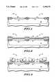
- FIGS. 1-8illustrate, in cross-sectional form, a method used to form a vertical bipolar transistor and a lateral bipolar transistor in accordance with the present invention.
- FIG. 1Illustrated in FIG. 1 is a structure suitable for formation of a vertical bipolar transistor 10 and a lateral bipolar transistor 11.
- the formation of transistor 10is similar to the formation of transistor 11. Therefore, various process flow steps described herein are discussed with reference to a single transistor.
- the transistors 10 and 11have a base layer or substrate 12 which has a surface 13.
- the substrateis of a first conductivity type wherein a conductivity type is either N type or P type.
- the transistor 10 or the transistor 11may be formed overlying another device or structure.
- the base layeris a conductive region, electrode, or conductive layer of the underlying device or structure.
- Substrate 12 or the base layermay be made of silicon, gallium arsenide, silicon on sapphire, epitaxial formations, germanium, germanium silicon, and/or like substrate materials. If substrate 12 is used as the base layer, the substrate 12 is preferably made of silicon.
- a doped diffused well 14is formed within the substrate 12 and exposed at the surface 13 of the substrate 12.
- the well 14is of a second conductivity type wherein the second conductivity type is opposite the first conductivity type.
- a diffusion 16is formed within the well 14 as explained below.
- the diffusion 16is of the first conductivity type.
- a field dielectric layer 18is formed adjacent active areas. Active areas are regions of either substrate 12, well 14, or diffusion 16 which are used for the formation of active devices, such as transistors 10 and 11.
- a screen dielectric layer 20is used for active area protection, improved diffusion formation, and other conventional purposes. The dielectric layer 20 may be removed subsequent to diffusion formation as illustrated in FIG. 2 or may remain on the surface of the substrate 12.
- a first dielectric layer 22is formed overlying substrate 12 and initially overlying the diffusion 16.
- a conductive layer 24is formed overlying the dielectric layer 22.
- conductive layer 24is polysilicon, but conductive layer 24 may be a metal, a salicide or silicide, germanium silicon, or the like.
- a second dielectric layer 26is formed overlying the conductive layer 24.
- the dielectric layers 22 and 26, and all other dielectrics described hereinmay vary in physical and chemical composition based upon the function they perform.
- the dielectric layers described hereinmay be wet or dry silicon dioxide (SiO 2 ), nitride, tetra-ethyl-ortho-silicate (TEOS) based oxides, boro-phosphate-silicate-glass (BPSG), phosphate-silicate-glass (PSG), boro-silicate-glass (BSG), oxide-nitride-oxide (ONO), tantalum pentoxide (Ta 2 O 5 ), plasma enhanced silicon nitride (P-SiN x ) and/or the like.
- SiO 2silicon dioxide
- nitridetetra-ethyl-ortho-silicate
- BPSGboro-phosphate-silicate-glass
- PSGphosphate-silicate-glass
- BSGboro-silicate-glass
- the doped glassmay be used as a dopant source. If a doped glass dopant source is undesirable, BPSG or PSG should be shielded by an undoped glass or should not be formed adjacent active areas. Specific dielectrics are noted herein if a specific dielectric is preferred or required.
- a masking layer 28which is preferably a layer of photoresist, is deposited overlying the dielectric layer 26.
- the masking layer 28is conventionally patterned and etched to form a mask opening for each of the transistors 10 and 11.
- the mask openingsexpose portions of the dielectric layer 26.
- the exposed portions of the dielectric layer 26are etched selective to the conductive layer 24 to form openings in the dielectric layer 26.
- Portions of the conductive layer 24are etched selective to the dielectric layer 22 to deepen the openings by etching into the conductive layer 24.
- the etching of the conductive layer 24forms a sidewall of the conductive layer 24 for each of the transistors 10 and 11. All of the openings are self-aligned to each other due to the masking layer 28.
- the sidewalls of the conductive layer 24are over-etched to laterally recess the sidewalls of the conductive layer 24 as illustrated in FIG. 3. Isotropic etching is usually used to accomplish the lateral recession of the sidewalls.
- the recession of the sidewalls of the conductive layer 24has advantages that are described herein. It is important to note that the recession of the sidewalls of the conductive layer 24 is optional.
- portions of the dielectric layer 22are etched selective to substrate 12 to further deepen the opening by etching into the dielectric layer 22.
- the etching of the dielectric layer 22exposes the surface of the diffusion 16 for transistor 10 and exposes a surface of the well 14 for transistor 11.
- the etching of the dielectric layers 22 and 26 and conductive layer 24results in an opening for each of the transistors 10 and 11 that is self-aligned to the mask openings.
- the openingsare referred to as device openings in most cases. It should be apparent that non-selective etching through the dielectric layer 26 and the conductive layer 24 may be used to form the device openings.
- the device openingscan be of any geometry or size but are each preferably a contact hole of minimum lithographic size.
- the diffusion 16is formed in one of at least two ways.
- the diffusion 16can be implanted or diffused into the substrate 12 selectively through the use of one of a photoresist mask, an oxide mask, a nitride mask or the like.
- Diffusion 16may be implanted through an oxide, such as dielectric layer 20 or a like material, to ensure a shallow, dopant-dispersed diffusion junction. This implantation or diffusion occurs before the formation of the conductive layer 24.
- the diffusion 16can be implanted or diffused after the formation of the device opening. The second method, when using ion implantation, is usually preferred due to the fact that the resulting diffusion 16 is self-aligned to the device openings of transistor 10 and 11.
- FIG. 4also illustrates a sidewall dielectric layer formation step.
- a sidewall dielectric layer 30is formed on the sidewalls of the conductive layer 24 that resulted from the formation of the device openings.
- the dielectric layer 30is preferably a grown SiO 2 layer. The growth of dielectric layer 30 will result in a thin dielectric layer 32 being grown on an exposed surface of the diffusion 16 for transistor 10 and on an exposed surface of the well 14 for transistor 11. In another form, the dielectric layer 30 could be formed via deposition technology or spacer formation technology.
- FIG. 5illustrates a dielectric removal step for the dielectric layer 32 along with an epitaxial growth step.
- a reactive ion etch (RIE) stepis used to remove the dielectric layer 32 from the surface of the substrate 12. Due to the fact that the sidewall dielectric layer 30 is formed on a recessed sidewall of the conductive layer 24, the RIE etch does not remove the sidewall dielectric layer 30.
- RIEreactive ion etch
- FIG. 5illustrates formation of a portion of a conductive region within each of the device openings.
- a grown conductive region 33is used to form all of the electrodes of the transistors 10 and 11.
- the conductive region 33is formed via epitaxial growth and is in-situ doped or implanted with dopants to form the conductive region 33 of the first conductivity type. It is important for electrical connection of the transistor 10 that the conductivity type of the conductive region 33 matches the conductivity type of the diffusion 16.
- the transistors 10 and 11are placed into conventional and commercially available equipment suitable for epitaxial growth. Growth is initiated by heating transistors 10 and 11 and subjecting exposed portions of the substrate 12 or diffusion 16 to a chemical compound such as dichloro-silane or a similar silicon source gas. It is important to note that epitaxial growth requires a clean surface. Therefore, before initiating growth a cleaning cycle, such as a conventional RCA oxidizing clean, an Ishizaka-Shiraki clean, or an equivalent cleaning cycle, is performed.
- a cleaning cyclesuch as a conventional RCA oxidizing clean, an Ishizaka-Shiraki clean, or an equivalent cleaning cycle, is performed.
- the sidewall dielectric layer 30is removed from the device opening of each of transistors 10 and 11.
- Dielectric layer 30is removed preferably by an isotropic etch step.
- a brief epitaxial growth stepis used to connect the conductive layer 24 to the conductive region 33 for each of the transistors 10 and 11.
- polysilicongrows from polysilicon and single-crystalline silicon grows from single-crystalline silicon.
- Epitaxial materialmay also form over metals and silicide. Therefore, the conductive layer 24 and conductive region 33 will grow towards each other and connect physically.
- conductive spacersmay be used to form electrical contact between the conductive layer 24 and the conductive region 33. The conductive spacers (not illustrated) must be subsequently isolated by a dielectric spacer (not illustrated) or the like.
- Spacer 34serves two primary functions and is preferably nitride. One function is that spacer 34 covers all exposed surfaces of conductive layer 24 to prevent conductive layer 24 from undergoing subsequent polysilicon growth during epitaxial processing steps. A second function is that the spacer can prevent electrodes from electrically short circuiting, in some cases. Active areas or electrodes, such as base electrodes, emitter electrodes, and control electrodes, containing or made of polysilicon are usually of poor quality when compared to single-crystalline or epitaxial silicon electrodes. Therefore, spacer 34 ensures that no polysilicon will epitaxially contribute to subsequent epitaxial electrode processing.
- the spacer 34is optional and not always necessary. If the conductive layer 24 is recessed significantly, as described herein, or if the sidewall dielectric layer 30 is made significantly thick, epitaxial growth of the conductive region 33 may connect to and pinch-off conductive layer 24 before the polysilicon of conductive layer 24 can epitaxially grow into the device opening. No spacer 34 is needed if pinch-off occurs.
- epitaxial growthcontinues to extend the conductive region 33 vertically between the spacer 34. This extension step is optional and is used to form a more planar topography.
- FIGS. 1-7the process flow for the transistors 10 and 11 is nearly identical with the exception of the diffusion 16.
- FIG. 8the processing for each of the transistors 10 and 11 varies. For this reason, transistor 10 is discussed first and transistor 11 is discussed in later paragraphs. Conventional masking techniques can be used to adequately protect transistor 10 when transistor 11 is being processed and vice versa.
- Transistor 10 of FIG. 8is implanted, dopant diffused, or insitu doped during prior growth to form an active base electrode region 36 from an upper portion of region 33.
- Region 36is doped with dopant atoms of the second conductivity type.
- a diffused region 42is formed adjacent the region 36 and is the same conductivity as the region 36.
- Region 42is formed by thermally driving dopant atoms of the second conductivity type from the conductive layer 24 into the region 36.
- Region 42may be two separated diffusions if conductive layer 24 is split into two electrically isolated regions by the formation of the device opening.
- the diffused region 42may completely surround the region 36 in a cylindrical diffused fashion if conductive layer 24 completely surrounds the device opening.
- a conductive layer 40is formed overlying the region 36.
- Conductive layer 40is doped with dopant atoms that are of the first conductivity type. Dopant atoms are thermally driven from the conductive layer 40 to form a current electrode region 38.
- a current electrodeis either an emitter electrode or a collector electrode.
- region 36 and region 42form a base electrode
- conductive layer 24forms a base electrode contact for transistor 10.
- Diffusion 16 and a remaining portion of region 33form either an emitter electrode or a collector electrode and a first current electrode electrical contact to the transistor 10.
- the conductive layer 40 and the region 38form either an emitter electrode or a collector electrode and a second current electrode electrical contact to the transistor 10.
- doping concentration and geometrydetermines which regions function as a collector electrode and which regions function as an emitter electrode.
- the emitter electrodeis doped with more dopant atoms than the collector electrode for optimal bipolar transistor operation. It is important to note that dopant atoms can thermally move between the diffusion 16 and the conductive region 33 to form other doped regions or diffusions.
- region 33functions as a base region of the first conductivity type.
- a conductive layer 40is formed overlying the region 33. Dopant atoms are thermally driven from the conductive layer 40 or dopant atoms are implanted to form a diffused base region 46. Together, regions 33 and 46 and conductive layer 40 function as a base electrode and base electrical contact.
- the conductive layer 24is separated or etched into two conductive electrically isolated regions via the formation of the device opening. Therefore, a diffused region 44 and a diffused region 48 are thermally formed from the two electrically separated regions of conductive layer 24. The diffused region 44 and the diffused region 48 are electrically isolated from each other.
- the diffused region 44 along with a connection to the conductive layer 24form either an emitter electrode or a collector electrode with an electrical connection.
- the diffused region 48 along with a connection to the conductive layer 24form either an emitter electrode or a collector electrode with an electrical connection.
- One emitter electrode and one collector electrodeis required. The emitter electrode is in most cases doped heavier than the collector electrode.
- Both lateral NPN and PNP transistorscan be formed, and both vertical NPN and PNP transistors may be formed by the inventive transistors described herein.
- the inventive method presented hereinprovides for either the independent formation or the simultaneous formation of lateral and/or vertical bipolar transistors.
- BiCMOS and bipolar circuitswhich have reduced substrate surface area, reduced leakage currents, and reduced capacitive parasitics will result via the transistors disclosed herein. Due to the fact that an electrode or base length of the transistor 10 is controlled by a region 36 thickness, many transistor electrode and base geometries will be independent from lithography, smaller than lithography allows, and controlled within a smaller variation.
- the effective base area of the transistors 10 and 11 and current pathsmay be reduced in area as compared with conventional bipolar transistors. Smaller base areas in the inventive transistors improve frequency response without increasing the complexity of the transistor processing.
- Base resistanceis decreased due to the geometry of the base contact. Silicon etch damage is limited due to the fact that subtractive techniques, such as silicon etching, are avoided. Base doping can be independently optimized to improve current drive. Greater isolation to the substrate is achieved.
- the transistors 10 and 11are formed within a contact which is lithographically the smallest feature size in an integrated circuit.
- the formation of the inventive transistorrequires few photolithography steps, and many features of the transistors 10 and 11 can be self-aligned.
- Asymmetric electrodesmay be formed and asymmetrical electrodes allow for greater circuit design flexibility than conventional bipolar transistors.
- epitaxial growth methodsvary in temperature, doping mechanisms, length of time, procedures, and chemistry, and most of these epitaxial processes are capable of forming the electrodes and regions of the inventive transistors and devices.
- Sidewall dielectricsmay be used in one of several ways and may even be used as sidewall gate dielectrics in BiCMOS processing and for transistor protection and isolation. Although sidewall dielectric formation is presented herein as a sidewall oxidation step, sidewall spacers may be used for sidewall dielectric formation or electrode formation.
Landscapes
- Engineering & Computer Science (AREA)
- Physics & Mathematics (AREA)
- Condensed Matter Physics & Semiconductors (AREA)
- General Physics & Mathematics (AREA)
- Manufacturing & Machinery (AREA)
- Computer Hardware Design (AREA)
- Microelectronics & Electronic Packaging (AREA)
- Power Engineering (AREA)
- Bipolar Transistors (AREA)
Abstract
Description
Claims (17)
Priority Applications (1)
| Application Number | Priority Date | Filing Date | Title |
|---|---|---|---|
| US07/856,314US5198375A (en) | 1992-03-23 | 1992-03-23 | Method for forming a bipolar transistor structure |
Applications Claiming Priority (1)
| Application Number | Priority Date | Filing Date | Title |
|---|---|---|---|
| US07/856,314US5198375A (en) | 1992-03-23 | 1992-03-23 | Method for forming a bipolar transistor structure |
Publications (1)
| Publication Number | Publication Date |
|---|---|
| US5198375Atrue US5198375A (en) | 1993-03-30 |
Family
ID=25323322
Family Applications (1)
| Application Number | Title | Priority Date | Filing Date |
|---|---|---|---|
| US07/856,314Expired - LifetimeUS5198375A (en) | 1992-03-23 | 1992-03-23 | Method for forming a bipolar transistor structure |
Country Status (1)
| Country | Link |
|---|---|
| US (1) | US5198375A (en) |
Cited By (10)
| Publication number | Priority date | Publication date | Assignee | Title |
|---|---|---|---|---|
| US5242843A (en)* | 1992-10-28 | 1993-09-07 | Allied-Signal Inc. | Method for making a heterojunction bipolar transistor with improved high frequency response |
| US5326718A (en)* | 1991-09-23 | 1994-07-05 | Siemens Aktiengesellschaft | Method for manufacturing a laterally limited, single-crystal region on a substrate and the employment thereof for the manufacture of an MOS transistor and a bipolar transistor |
| US5340754A (en)* | 1992-09-02 | 1994-08-23 | Motorla, Inc. | Method for forming a transistor having a dynamic connection between a substrate and a channel region |
| EP0651443A1 (en)* | 1993-11-01 | 1995-05-03 | Nec Corporation | Integrated structure comprising a vertical and a laterial bipolar transistor |
| US5686322A (en)* | 1995-03-17 | 1997-11-11 | Harris Corporation | Process for doping two levels of a double poly bipolar transistor after formation of second poly layer |
| US5952706A (en)* | 1997-10-29 | 1999-09-14 | National Semiconductor Corporation | Semiconductor integrated circuit having a lateral bipolar transistor compatible with deep sub-micron CMOS processing |
| US6284633B1 (en)* | 1997-11-24 | 2001-09-04 | Motorola Inc. | Method for forming a tensile plasma enhanced nitride capping layer over a gate electrode |
| US6404038B1 (en) | 2000-03-02 | 2002-06-11 | The United States Of America As Represented By The Secretary Of The Navy | Complementary vertical bipolar junction transistors fabricated of silicon-on-sapphire utilizing wide base PNP transistors |
| US20060105532A1 (en)* | 2004-11-16 | 2006-05-18 | Atmel Germany Gmbh | Integrated circuit and method for manufacturing an integrated circuit on a chip |
| US9105650B2 (en) | 2012-09-12 | 2015-08-11 | International Business Machines Corporation | Lateral bipolar transistor and CMOS hybrid technology |
Citations (11)
| Publication number | Priority date | Publication date | Assignee | Title |
|---|---|---|---|---|
| US4663831A (en)* | 1985-10-08 | 1987-05-12 | Motorola, Inc. | Method of forming transistors with poly-sidewall contacts utilizing deposition of polycrystalline and insulating layers combined with selective etching and oxidation of said layers |
| US4696097A (en)* | 1985-10-08 | 1987-09-29 | Motorola, Inc. | Poly-sidewall contact semiconductor device method |
| US4703554A (en)* | 1985-04-04 | 1987-11-03 | Texas Instruments Incorporated | Technique for fabricating a sidewall base contact with extrinsic base-on-insulator |
| US4786615A (en)* | 1987-08-31 | 1988-11-22 | Motorola Inc. | Method for improved surface planarity in selective epitaxial silicon |
| US4824799A (en)* | 1985-01-17 | 1989-04-25 | Kabushiki Kaisha Toshiba | Method of making a bipolar semiconductor device |
| US4849371A (en)* | 1986-12-22 | 1989-07-18 | Motorola Inc. | Monocrystalline semiconductor buried layers for electrical contacts to semiconductor devices |
| US4851362A (en)* | 1987-08-25 | 1989-07-25 | Oki Electric Industry Co., Ltd. | Method for manufacturing a semiconductor device |
| US4860077A (en)* | 1987-09-28 | 1989-08-22 | Motorola, Inc. | Vertical semiconductor device having a sidewall emitter |
| US4876212A (en)* | 1987-10-01 | 1989-10-24 | Motorola Inc. | Process for fabricating complimentary semiconductor devices having pedestal structures |
| US4902641A (en)* | 1987-07-31 | 1990-02-20 | Motorola, Inc. | Process for making an inverted silicon-on-insulator semiconductor device having a pedestal structure |
| US4997775A (en)* | 1990-02-26 | 1991-03-05 | Cook Robert K | Method for forming a complementary bipolar transistor structure including a self-aligned vertical PNP transistor |
- 1992
- 1992-03-23USUS07/856,314patent/US5198375A/ennot_activeExpired - Lifetime
Patent Citations (11)
| Publication number | Priority date | Publication date | Assignee | Title |
|---|---|---|---|---|
| US4824799A (en)* | 1985-01-17 | 1989-04-25 | Kabushiki Kaisha Toshiba | Method of making a bipolar semiconductor device |
| US4703554A (en)* | 1985-04-04 | 1987-11-03 | Texas Instruments Incorporated | Technique for fabricating a sidewall base contact with extrinsic base-on-insulator |
| US4663831A (en)* | 1985-10-08 | 1987-05-12 | Motorola, Inc. | Method of forming transistors with poly-sidewall contacts utilizing deposition of polycrystalline and insulating layers combined with selective etching and oxidation of said layers |
| US4696097A (en)* | 1985-10-08 | 1987-09-29 | Motorola, Inc. | Poly-sidewall contact semiconductor device method |
| US4849371A (en)* | 1986-12-22 | 1989-07-18 | Motorola Inc. | Monocrystalline semiconductor buried layers for electrical contacts to semiconductor devices |
| US4902641A (en)* | 1987-07-31 | 1990-02-20 | Motorola, Inc. | Process for making an inverted silicon-on-insulator semiconductor device having a pedestal structure |
| US4851362A (en)* | 1987-08-25 | 1989-07-25 | Oki Electric Industry Co., Ltd. | Method for manufacturing a semiconductor device |
| US4786615A (en)* | 1987-08-31 | 1988-11-22 | Motorola Inc. | Method for improved surface planarity in selective epitaxial silicon |
| US4860077A (en)* | 1987-09-28 | 1989-08-22 | Motorola, Inc. | Vertical semiconductor device having a sidewall emitter |
| US4876212A (en)* | 1987-10-01 | 1989-10-24 | Motorola Inc. | Process for fabricating complimentary semiconductor devices having pedestal structures |
| US4997775A (en)* | 1990-02-26 | 1991-03-05 | Cook Robert K | Method for forming a complementary bipolar transistor structure including a self-aligned vertical PNP transistor |
Cited By (14)
| Publication number | Priority date | Publication date | Assignee | Title |
|---|---|---|---|---|
| US5326718A (en)* | 1991-09-23 | 1994-07-05 | Siemens Aktiengesellschaft | Method for manufacturing a laterally limited, single-crystal region on a substrate and the employment thereof for the manufacture of an MOS transistor and a bipolar transistor |
| US5527723A (en)* | 1992-09-02 | 1996-06-18 | Motorola, Inc. | Method for forming a dynamic contact which can be either on or off or switched therebetween |
| US5340754A (en)* | 1992-09-02 | 1994-08-23 | Motorla, Inc. | Method for forming a transistor having a dynamic connection between a substrate and a channel region |
| US5393681A (en)* | 1992-09-02 | 1995-02-28 | Motorola, Inc. | Method for forming a compact transistor structure |
| US5627395A (en)* | 1992-09-02 | 1997-05-06 | Motorola Inc. | Vertical transistor structure |
| US5242843A (en)* | 1992-10-28 | 1993-09-07 | Allied-Signal Inc. | Method for making a heterojunction bipolar transistor with improved high frequency response |
| EP0651443A1 (en)* | 1993-11-01 | 1995-05-03 | Nec Corporation | Integrated structure comprising a vertical and a laterial bipolar transistor |
| US5508553A (en)* | 1993-11-01 | 1996-04-16 | Nec Corporation | Transversal bipolar transistor integrated with another transistor commonly provided on a semiconductor substrate |
| US5686322A (en)* | 1995-03-17 | 1997-11-11 | Harris Corporation | Process for doping two levels of a double poly bipolar transistor after formation of second poly layer |
| US5952706A (en)* | 1997-10-29 | 1999-09-14 | National Semiconductor Corporation | Semiconductor integrated circuit having a lateral bipolar transistor compatible with deep sub-micron CMOS processing |
| US6284633B1 (en)* | 1997-11-24 | 2001-09-04 | Motorola Inc. | Method for forming a tensile plasma enhanced nitride capping layer over a gate electrode |
| US6404038B1 (en) | 2000-03-02 | 2002-06-11 | The United States Of America As Represented By The Secretary Of The Navy | Complementary vertical bipolar junction transistors fabricated of silicon-on-sapphire utilizing wide base PNP transistors |
| US20060105532A1 (en)* | 2004-11-16 | 2006-05-18 | Atmel Germany Gmbh | Integrated circuit and method for manufacturing an integrated circuit on a chip |
| US9105650B2 (en) | 2012-09-12 | 2015-08-11 | International Business Machines Corporation | Lateral bipolar transistor and CMOS hybrid technology |
Similar Documents
| Publication | Publication Date | Title |
|---|---|---|
| US4960726A (en) | BiCMOS process | |
| US5414288A (en) | Vertical transistor having an underlying gate electrode contact | |
| JP3301062B2 (en) | High performance MOSFET device with raised source and drain and method of forming the same | |
| US5166767A (en) | Sidewall contact bipolar transistor with controlled lateral spread of selectively grown epitaxial layer | |
| JP3217179B2 (en) | Vertically integrated semiconductor structure | |
| US4318751A (en) | Self-aligned process for providing an improved high performance bipolar transistor | |
| US5171702A (en) | Method for forming a thick base oxide in a BiCMOS process | |
| US4897703A (en) | Recessed contact bipolar transistor and method | |
| JPH01124261A (en) | Manufacture of semiconductor device | |
| EP0369336A2 (en) | Process for fabricating bipolar and CMOS transistors on a common substrate | |
| JPH07105392B2 (en) | Semiconductor device structure having protrusions | |
| US5204277A (en) | Method of forming bipolar transistor having substrate to polysilicon extrinsic base contact | |
| US5198375A (en) | Method for forming a bipolar transistor structure | |
| JP2937253B2 (en) | Semiconductor device and manufacturing method thereof | |
| JPH09181089A (en) | Method of manufacturing super self-aligned bipolar transistor | |
| KR100401036B1 (en) | A method of manufacturing a self-aligend vertical bipolar transistor on an soi | |
| JPS63292674A (en) | Vertical bipolar transistor and its manufacturing method | |
| US4957875A (en) | Vertical bipolar transistor | |
| US20030107051A1 (en) | Super self -aligned heterojunction biplar transistor and its manufacturing method | |
| US6753234B1 (en) | Method of forming the silicon germanium base of a bipolar transistor | |
| EP0036499A1 (en) | A polysilicon-base self-aligned bipolar transistor process | |
| US4982257A (en) | Vertical bipolar transistor with collector and base extensions | |
| KR100257517B1 (en) | Structure and method of high speed bipolar transistor | |
| EP0287318B1 (en) | Integrated transistor and manufacturing process therefor | |
| US6444536B2 (en) | Method for fabricating bipolar transistors |
Legal Events
| Date | Code | Title | Description |
|---|---|---|---|
| AS | Assignment | Owner name:MOTOROLA, INC. A CORP. OF DELAWARE, ILLINOIS Free format text:ASSIGNMENT OF ASSIGNORS INTEREST.;ASSIGNORS:HAYDEN, JAMES D.;MAZURE', CARLOS A.;FITCH, JON T.;REEL/FRAME:006068/0675 Effective date:19920317 | |
| STCF | Information on status: patent grant | Free format text:PATENTED CASE | |
| FPAY | Fee payment | Year of fee payment:4 | |
| FPAY | Fee payment | Year of fee payment:8 | |
| FEPP | Fee payment procedure | Free format text:PAYOR NUMBER ASSIGNED (ORIGINAL EVENT CODE: ASPN); ENTITY STATUS OF PATENT OWNER: LARGE ENTITY | |
| AS | Assignment | Owner name:FREESCALE SEMICONDUCTOR, INC., TEXAS Free format text:ASSIGNMENT OF ASSIGNORS INTEREST;ASSIGNOR:MOTOROLA, INC.;REEL/FRAME:015698/0657 Effective date:20040404 Owner name:FREESCALE SEMICONDUCTOR, INC.,TEXAS Free format text:ASSIGNMENT OF ASSIGNORS INTEREST;ASSIGNOR:MOTOROLA, INC.;REEL/FRAME:015698/0657 Effective date:20040404 | |
| FPAY | Fee payment | Year of fee payment:12 | |
| AS | Assignment | Owner name:CITIBANK, N.A. AS COLLATERAL AGENT, NEW YORK Free format text:SECURITY AGREEMENT;ASSIGNORS:FREESCALE SEMICONDUCTOR, INC.;FREESCALE ACQUISITION CORPORATION;FREESCALE ACQUISITION HOLDINGS CORP.;AND OTHERS;REEL/FRAME:018855/0129 Effective date:20061201 Owner name:CITIBANK, N.A. AS COLLATERAL AGENT,NEW YORK Free format text:SECURITY AGREEMENT;ASSIGNORS:FREESCALE SEMICONDUCTOR, INC.;FREESCALE ACQUISITION CORPORATION;FREESCALE ACQUISITION HOLDINGS CORP.;AND OTHERS;REEL/FRAME:018855/0129 Effective date:20061201 | |
| AS | Assignment | Owner name:CITIBANK, N.A., AS COLLATERAL AGENT,NEW YORK Free format text:SECURITY AGREEMENT;ASSIGNOR:FREESCALE SEMICONDUCTOR, INC.;REEL/FRAME:024397/0001 Effective date:20100413 Owner name:CITIBANK, N.A., AS COLLATERAL AGENT, NEW YORK Free format text:SECURITY AGREEMENT;ASSIGNOR:FREESCALE SEMICONDUCTOR, INC.;REEL/FRAME:024397/0001 Effective date:20100413 | |
| AS | Assignment | Owner name:FREESCALE SEMICONDUCTOR, INC., TEXAS Free format text:PATENT RELEASE;ASSIGNOR:CITIBANK, N.A., AS COLLATERAL AGENT;REEL/FRAME:037354/0225 Effective date:20151207 Owner name:FREESCALE SEMICONDUCTOR, INC., TEXAS Free format text:PATENT RELEASE;ASSIGNOR:CITIBANK, N.A., AS COLLATERAL AGENT;REEL/FRAME:037356/0143 Effective date:20151207 Owner name:FREESCALE SEMICONDUCTOR, INC., TEXAS Free format text:PATENT RELEASE;ASSIGNOR:CITIBANK, N.A., AS COLLATERAL AGENT;REEL/FRAME:037356/0553 Effective date:20151207 |