US5197893A - Connector assembly for printed circuit boards - Google Patents
Connector assembly for printed circuit boardsDownload PDFInfo
- Publication number
- US5197893A US5197893AUS07/844,992US84499292AUS5197893AUS 5197893 AUS5197893 AUS 5197893AUS 84499292 AUS84499292 AUS 84499292AUS 5197893 AUS5197893 AUS 5197893A
- Authority
- US
- United States
- Prior art keywords
- contacts
- ground
- contact
- connector element
- signal
- Prior art date
- Legal status (The legal status is an assumption and is not a legal conclusion. Google has not performed a legal analysis and makes no representation as to the accuracy of the status listed.)
- Expired - Lifetime
Links
Images


Classifications
- H—ELECTRICITY
- H01—ELECTRIC ELEMENTS
- H01R—ELECTRICALLY-CONDUCTIVE CONNECTIONS; STRUCTURAL ASSOCIATIONS OF A PLURALITY OF MUTUALLY-INSULATED ELECTRICAL CONNECTING ELEMENTS; COUPLING DEVICES; CURRENT COLLECTORS
- H01R12/00—Structural associations of a plurality of mutually-insulated electrical connecting elements, specially adapted for printed circuits, e.g. printed circuit boards [PCB], flat or ribbon cables, or like generally planar structures, e.g. terminal strips, terminal blocks; Coupling devices specially adapted for printed circuits, flat or ribbon cables, or like generally planar structures; Terminals specially adapted for contact with, or insertion into, printed circuits, flat or ribbon cables, or like generally planar structures
- H01R12/70—Coupling devices
- H01R12/71—Coupling devices for rigid printing circuits or like structures
- H01R12/72—Coupling devices for rigid printing circuits or like structures coupling with the edge of the rigid printed circuits or like structures
- H01R12/73—Coupling devices for rigid printing circuits or like structures coupling with the edge of the rigid printed circuits or like structures connecting to other rigid printed circuits or like structures
- H01R12/735—Printed circuits including an angle between each other
- H01R12/737—Printed circuits being substantially perpendicular to each other
- H—ELECTRICITY
- H01—ELECTRIC ELEMENTS
- H01R—ELECTRICALLY-CONDUCTIVE CONNECTIONS; STRUCTURAL ASSOCIATIONS OF A PLURALITY OF MUTUALLY-INSULATED ELECTRICAL CONNECTING ELEMENTS; COUPLING DEVICES; CURRENT COLLECTORS
- H01R12/00—Structural associations of a plurality of mutually-insulated electrical connecting elements, specially adapted for printed circuits, e.g. printed circuit boards [PCB], flat or ribbon cables, or like generally planar structures, e.g. terminal strips, terminal blocks; Coupling devices specially adapted for printed circuits, flat or ribbon cables, or like generally planar structures; Terminals specially adapted for contact with, or insertion into, printed circuits, flat or ribbon cables, or like generally planar structures
- H01R12/70—Coupling devices
- H01R12/71—Coupling devices for rigid printing circuits or like structures
- H01R12/712—Coupling devices for rigid printing circuits or like structures co-operating with the surface of the printed circuit or with a coupling device exclusively provided on the surface of the printed circuit
- H01R12/716—Coupling device provided on the PCB
- H—ELECTRICITY
- H01—ELECTRIC ELEMENTS
- H01R—ELECTRICALLY-CONDUCTIVE CONNECTIONS; STRUCTURAL ASSOCIATIONS OF A PLURALITY OF MUTUALLY-INSULATED ELECTRICAL CONNECTING ELEMENTS; COUPLING DEVICES; CURRENT COLLECTORS
- H01R12/00—Structural associations of a plurality of mutually-insulated electrical connecting elements, specially adapted for printed circuits, e.g. printed circuit boards [PCB], flat or ribbon cables, or like generally planar structures, e.g. terminal strips, terminal blocks; Coupling devices specially adapted for printed circuits, flat or ribbon cables, or like generally planar structures; Terminals specially adapted for contact with, or insertion into, printed circuits, flat or ribbon cables, or like generally planar structures
- H01R12/70—Coupling devices
- H01R12/71—Coupling devices for rigid printing circuits or like structures
- H01R12/72—Coupling devices for rigid printing circuits or like structures coupling with the edge of the rigid printed circuits or like structures
- H01R12/722—Coupling devices for rigid printing circuits or like structures coupling with the edge of the rigid printed circuits or like structures coupling devices mounted on the edge of the printed circuits
- H01R12/724—Coupling devices for rigid printing circuits or like structures coupling with the edge of the rigid printed circuits or like structures coupling devices mounted on the edge of the printed circuits containing contact members forming a right angle
- H—ELECTRICITY
- H01—ELECTRIC ELEMENTS
- H01R—ELECTRICALLY-CONDUCTIVE CONNECTIONS; STRUCTURAL ASSOCIATIONS OF A PLURALITY OF MUTUALLY-INSULATED ELECTRICAL CONNECTING ELEMENTS; COUPLING DEVICES; CURRENT COLLECTORS
- H01R13/00—Details of coupling devices of the kinds covered by groups H01R12/70 or H01R24/00 - H01R33/00
- H01R13/648—Protective earth or shield arrangements on coupling devices, e.g. anti-static shielding
- H01R13/658—High frequency shielding arrangements, e.g. against EMI [Electro-Magnetic Interference] or EMP [Electro-Magnetic Pulse]
- H01R13/6581—Shield structure
- H01R13/6585—Shielding material individually surrounding or interposed between mutually spaced contacts
- H01R13/6586—Shielding material individually surrounding or interposed between mutually spaced contacts for separating multiple connector modules
- H01R13/6587—Shielding material individually surrounding or interposed between mutually spaced contacts for separating multiple connector modules for mounting on PCBs
- H—ELECTRICITY
- H01—ELECTRIC ELEMENTS
- H01R—ELECTRICALLY-CONDUCTIVE CONNECTIONS; STRUCTURAL ASSOCIATIONS OF A PLURALITY OF MUTUALLY-INSULATED ELECTRICAL CONNECTING ELEMENTS; COUPLING DEVICES; CURRENT COLLECTORS
- H01R13/00—Details of coupling devices of the kinds covered by groups H01R12/70 or H01R24/00 - H01R33/00
- H01R13/648—Protective earth or shield arrangements on coupling devices, e.g. anti-static shielding
- H01R13/658—High frequency shielding arrangements, e.g. against EMI [Electro-Magnetic Interference] or EMP [Electro-Magnetic Pulse]
- H01R13/6591—Specific features or arrangements of connection of shield to conductive members
- H01R13/6592—Specific features or arrangements of connection of shield to conductive members the conductive member being a shielded cable
- H—ELECTRICITY
- H01—ELECTRIC ELEMENTS
- H01R—ELECTRICALLY-CONDUCTIVE CONNECTIONS; STRUCTURAL ASSOCIATIONS OF A PLURALITY OF MUTUALLY-INSULATED ELECTRICAL CONNECTING ELEMENTS; COUPLING DEVICES; CURRENT COLLECTORS
- H01R24/00—Two-part coupling devices, or either of their cooperating parts, characterised by their overall structure
- H01R24/38—Two-part coupling devices, or either of their cooperating parts, characterised by their overall structure having concentrically or coaxially arranged contacts
- H01R24/40—Two-part coupling devices, or either of their cooperating parts, characterised by their overall structure having concentrically or coaxially arranged contacts specially adapted for high frequency
- H01R24/50—Two-part coupling devices, or either of their cooperating parts, characterised by their overall structure having concentrically or coaxially arranged contacts specially adapted for high frequency mounted on a PCB [Printed Circuit Board]
Definitions
- the inventionrelates to a connector assembly for printed circuit boards, comprising a first connector element with a first housing of insulating material and regularly arranged male signal and ground contacts connectable to a printed circuit board, and a second connector element with a second housing of insulating material, which can be inserted with an insertion side into the first housing, and with regularly arranged female signal and ground contacts with a connection element, which female contacts will contact the corresponding male contacts when the second housing is received in the first housing.
- Such connector assembliesare known in various embodiments.
- attentionhas mainly been paid to the mechanical aspects of the connector assembly, in particular with respect to the forces required for coupling and decoupling the connector elements.
- Attentionwas only paid to the electrical aspects in that one aimed at realizing good reliable connections between the contacts of both connector elements.
- the electrical performance of the contacts as a circuit elementbecomes important.
- problemsoccur with higher signal speeds with respect to cross-over between signal contacts, transmission losses, reflections and ground bounce or switching noise. Despite an optimal distribution of the ground and signal contacts these problems cannot be eliminated below rise times of 0.6 ns in the known connector assemblies.
- the inventionaims to provide a connector assembly of the above-mentioned type wherein the problems occurring at high signal speeds in the known connector assemblies can be obviated by making the connector elements in such a manner that the performance of the contacts as a circuit element can be previously determined and said signal distortions are minimized.
- the connector assembly according to the inventionis characterized in that said second connector element is provided with a plurality o ⁇ outer conductors, each of said outer conductors mainly enclosing at least one signal contact in a circumferential direction and each of said outer conductors being adapted to contact the adjacent ground contacts of the/each corresponding signal contact of the first connector element.
- the connector assembly according to the inventionshows the advantage that the connector elements and the male and female contacts can be made in a usual manner so that all known design and manufacturing techniques of the usual connector assemblies can be used advantageously.
- the connection between the male and female contactsis comparable with the same of the known connector assemblies so that the favourable mechanical properties thereof, such as coupling/decoupling forces and in particular the tolerances with respect to the mutual positions of the contacts are maintained when used in rack and panel configurations.
- all contacts and outer connectorscan be manufactured from metal strips by stamping and forming so that the manufacturing costs of the connector assembly according to the invention are low.
- each signal contact of the second connector elementis mounted in the corresponding outer conductor by means of a dielectric insert.
- the impedance of each signal contactcan be determined by using an insert wherein by providing more or less recesses the dielectric constant of the insert between the signal contact and the outer conductor can be determined.
- the combination of signal contact and outer conductor which can be considered as a transmission line,can be provided with a desired impedance.
- FIG. 1is a section of a first embodiment of a connector assembly wherein the first and second connector elements are shown in a disassembled position.
- FIG. 2is a section corresponding with FIG. 1 of an amended embodiment of the connector assembly according to the invention.
- FIG. 3is a top view of the first connector element of FIGS. 1 and 2.
- FIGS. 4a and 4bshow perspective the ground contact plates of the second connector element of FIGS. 1 and 2, respectively.
- FIG. 5is a partially shown perspective cut-away view of the second connector element of the connector assembly of FIG. 1.
- FIG. 6is a section corresponding with FIG. 1 of an amended embodiment of the connector assembly according to the invention.
- FIG. 7is a perspective view of an amended embodiment of the outer conductor and corresponding signal contact as the same can be used in the second connector element.
- FIG. 8is a partially shown perspective cut-away view of an amended embodiment of the second connector element of a connector assembly according to the invention.
- FIG. 8ais a perspective view of an outer conductor of the connector element of FIG. 8 with dielectric insert.
- FIG. 9is a schematic section of the connector element of FIG. 8 to explain the ground connection.
- FIG. 10is a section corresponding with FIG. 1 of an amended embodiment of the connector assembly according to the invention.
- FIG. 11is a perspective view of the outer conductors of the second connector element of the connector assembly according to FIG. 10.
- FIG. 12is a perspective view of a ground contact of the first connector element of the connector assembly according to FIG. 10.
- FIG. 13shows in perspective an outer conductor of the second connector element with two female signal contacts.
- FIG. 14is a top view of an alternative embodiment of the first connector element according to the invention.
- FIG. 15is a section according to the line XV--XV of FIG. 14.
- FIG. 16a perspective view of an outer conductor with signal contact of the first connector element of FIG. 14.
- FIG. 17is a section corresponding with FIG. 15 of a first connector element with amended connection to a printed circuit board.
- FIG. 18shows in perspective the outer conductors with signal contacts of the connector element of FIG. 17.
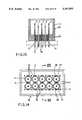
- FIG. 1there is shown a cross-section of a connector assembly 1 comprising a first connector element 2 with a first housing 3 of insulating material and contact pins 4 and 5 arranged in parallel rows r and columns c (see FIG. 3).
- These contact pins 4, 5each have a connection element 6, by which the contact pins 4, 5 can be connected with the plated inner wall of holes in a printed circuit board 7 indicated by a dashed.
- the connection elements 6are preferably provided with a known press-fit portion not further shown.
- the connector element 2comprises two rows with signal contact pins 4 which are indicated by an s, wherein at both sides of each row with only signal contact pins 4 a row with only ground contact pins 5 indicated by a g is provided.
- the arrangementis such that a column with only ground contact pins 5 is provided on both sides of each column c with alternatingly signal contact pins 4 and ground contact pins 5.
- the rows with contact pins 4, 5have a fixed intermediate spacing of 2 mm, while in row direction the ground contact pins 5 lie at a fixed intermediate spacing of 2 mm and the signal contact pins 4 lie at a fixed intermediate spacing of 4 mm.
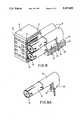
- the connector assembly 1is further provided with a second connector element 8 with a second housing 9 of insulating material adapted to be inserted with an insertion side 10 in the first housing 3 of the connector element 2.
- the second connector element 8is shown in perspective in FIG. 5 and includes two rows with female signal contacts 11 for contacting the signal contact pins 4 when the second housing 9 is received in the first housing 3.
- Each signal contact 11is enclosed by an outer conductor 12 which seen in column direction has opposite contact springs 13.
- Each of the outer conductors 12substantially entirely circumferentially encloses at least one of the signal contact pins 4. In inserted position these contact springs 13 contact the ground contact pins 5 of the first connector element 2 lying in the same column as the corresponding signal contact pin 4.
- the outer conductors 12Seen in row direction the outer conductors 12 have opposite contact tongues 14 adapted to contact ground contact plates 15 located on both sides of each outer conductor 12 in the second housing 9
- the contact tongues 14 lying at the insertion side in FIG. 5conduct the current to the inner side of the outer conductor 12 whereas the contact tongues 14 lying at the other end conduct the current from the inner side of the outer conductor to the ground contact plates 15.
- FIG. 4ashows one ground contact plate 15 in perspective.
- This ground contact plate 15is provided with female contact elements 16 at the insertion side, which contact elements 16 cooperate with the columns with only ground contact pins 5 of the first connector element 2. In this manner a very good ground connection between both connector elements 2, 8 is obtained, wherein a favourable current distribution in the outer conductors 12 occurs.
- connection elements 17 and 18are provided with a press-fit portion.
- ground contact plates 15can be closed by providing a ground contact plate 15 with extensions which extend from this ground contact plate 15 to the adjacent ground contact plate 15. Thereby the signal contacts 11 will be fully enclosed by ground contact plates.
- the signal contacts 11Due to the fact that the signal contacts 11 are surrounded by the outer conductors 12 and are further enclosed between the ground contact plates 15, the signal contacts 11 with the outer conductor 12/ground contact plates 15 form a transmission line with a geometry, of which the electrical parameters and thereby the performance as circuit element can be determined.
- the signal contacts 11are mounted in the outer conductors 12 by means of dielectric inserts 19. These dielectric inserts 19 which can be manufactured by injection molding at low costs, have a predetermined dielectric constant. By providing larger or smaller recesses so that more or less air is present between the signal contacts 11 and the outer conductors 12, this dielectric constant can be determined and thereby among others the impedance of the transmission line formed by the signal contacts 11 and the outer conductors 12/ground contact plates 15. In this manner a connection can be realized with a constant impedance, wherein cross-over between signal contacts cannot occur because each signal conductor is surrounded by a ground conductor.
- connection elements 17, 18 of the signal contacts 11 and the ground contact plates 15may also be made as contact springs adapted for surface mounting as appears from FIG. 2, showing a connector assembly, the connector element 2 of which fully corresponds with the connector element 2 of FIG. 1 and the connector element 8 of which is provided with ground contact plates 20 and signal contacts 11 adapted for surface mounting.
- the connection elementsare indicated by 17' and 18'.
- FIG. 4bshows in perspective a ground contact plate 20 used in the embodiment according to FIG. 2.
- FIG. 6shows a cross-section of a connector assembly 21 mainly made in the same manner as the connector assembly according to FIG. 2.
- two rows of ground contact pins 5are mounted between the two rows of signal contact pins 4.
- Ground contact plates 23each having a contact spring 18' are used, which contact plates 23 can only contact the ground contact pins 5 on both sides of the corresponding signal contact pins 4. Thereby separated ground connections for the two rows of signal contact pins 4 are obtained.
- Due to the increased width of the connector assembly 21it is also possible to use a printed circuit board 22 with increased thickness.
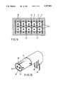
- FIG. 7shows in perspective one outer conductor 24 which can be mounted in the second connector element 8 for connecting coaxial cables 25 to the printed circuit board 7.
- the outer conductor 24comprises a connection element 26 to provide a simple connection with the outer conductor 27 of the coaxial cable 25. T this end the connection element 26 is first bent around the outer conductor 27.
- the signal contact not further shown and mounted in the outer conductor 24 by the dielectric insert 19,has a connection element 28 for connecting the inner conductor 29 of the coaxial cable 25.
- the connection between the outer conductor 27 and the inner conductor 29can be obtained by soldering.
- FIG. 8shows a perspective view of an amended embodiment of the second connector element 8 with the housing 9, wherein the outer conductors 12 at the side opposite of the insertion side 10 are provided with an extension 31 having two ground contact pins 32 to be connected to a printed circuit board 33.
- FIG. 8aone of the outer conductors with dielectric insert 19 and both ground contact pins 32 is shown in perspective.
- the ground contact pins 32can be provided with a press-fit portion.
- the contact pins 32are lying with respect to the longitudinal direction of the outer conductor 12 diagonally with respect to each other. Straight opposite of each contact pin 32 a recess 34 is provided, leaving free a hole 35 of the printed circuit board 33 which is intended to receive the ground contact pin 32 of an adjacent outer conductor 12.
- FIG. 9schematically shows a section of the housing 9 of the connector element 8, wherein for the sake of clearness the outer conductors 12 and the inserts 19 are not shown.
- the signal contacts 11are indicated by an open rectangle, whereas the locations for the contact pins 4, 5 are indicated by shaded squares.
- ground contact plates 36are used which are separated for the two rows of signal contact pins 4 and which are indicated in FIG. 9 by an oblique shading.
- ground contact plates 36have only one female contact element 16 which can only contact a corresponding ground contact pin 5 of the outermost rows of ground contact pins 5.
- insulating plates 37are provided at three locations in the housing 9 of the second connector element 8, while in the middle row of ground contact pins 5 only one ground contact pin 5 is mounted and four non-conductive insulating pins 38 (also horizontally shaded).
- the outer conductors 12 of different groups of signal contact pins 4 and corresponding female signal contacts 11are insulated with respect to each other, so that the ground connection of these groups is separated and these groups cannot effect each other.
- each desired group of signal contacts with common ground connectioncan be realized. It is noted that instead of insulating pins 38 it is sufficient just to omit the ground contact pins 5 for separating the outer conductors 12 lying in one column.
- the ground contact plates 36can also be coated on one side with an insulating layer to obtain a separation between adjacent outer conductors 12. Thereby not only a separation is possible but the outer conductor 12 lying at the conductive side of the ground contact plate 36 maintains its ground connection through this ground contact plate.
- FIG. 10shows a cross-section of a connector assembly 39, wherein the first connector element 40 mainly corresponds with the first connector element of FIG. 1.
- the contact pins 4, 5are located in column direction at a mutual distance of 2.5 mm.
- the signal contact pins 4lie at an intermediate spacing of 4.5 mm.
- Each three subsequent ground contact pins 5are united into a ground contact lip 41 shown in FIG. 12, which can have three connection elements 42 with a mutual spacing of 1.5 mm.
- the connector assembly 39comprises a second connector element 43 which in the same manner as the second connector element 8 is provided with two rows of female signal contacts.
- the second connector element 43further comprises for each signal contact an outer conductor 44 and 45, respectively, having an extension 46 and 47, respectively.
- the outer conductors 44, 45are perspectively shown in FIG. 11.
- the extensions 46, 47have four connection elements 48 which may be provided with a press-fit portion.
- the outer conductors 44, 45further have two contact springs 49 on both sides for contacting the ground contact lips 41 which are adjacent on both sides of the corresponding signal contact pin 4 of the first connector element 40. Thereby the ground connection is separated for each column of signal contacts. If two rows of ground contact pins 5 are provided between both rows of signal contact pins 4 as in the embodiment of FIG. 6, each signal contact pin 4 can have a separated ground connection.
- each female signal contactis mounted in the corresponding outer conductor 44, 45 also by means of a dielectric insert in the connector assembly 39.
- FIG. 10two connection elements 50 of the female signal contacts of the second connector element 43 are shown.
- connection elementsfor mounting in plated holes of a printed circuit board.
- connection elementscan be made as contact springs for surface mounting.
- each female signal contactis enclosed by an outer conductor
- twinax or triax connectionswith the same favourable properties can be obtained.
- the connector assembly according to the inventionis therefor for example also suitable for use in systems equiped with ECL circuits.
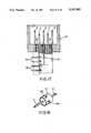
- FIG. 13shows in perspective as an example an outer conductor 51 of a second connector element not shown, in which two female signal contacts 52 are mounted by means of an insert 53.
- the outer conductor 51comprises ground connection elements 54, whereas the signal contacts 52 each have a connection element 55. Further the outer conductor 51 is provided with contact springs 56 for contacting ground contacts of the corresponding signal contact of the first connector element not shown. It will be clear that both connector elements can be made in the above-described manner for the remaining part.
- the described connector assembliesalready give a substantial improvement as to the high frequency performance. A further improvement can even be obtained if the signal contacts of the first connector element are mounted in an outer conductor in the same manner as the signal contacts of the second connector element.
- FIGS. 14 and 15show a top view and a section, respectively, of a first connector element 56, wherein each signal contact 4 is enclosed by an outer conductor 57 along the portion of the signal contact extending in the insulating material of the first housing 3.
- the signal contacts 4are in this case mounted in the outer conductor 57 be means of an insert 58. It is noted that in this case also two or more signal contacts 4 can be enclosed by a common outer conductor 57.
- the ground contacts 5 of the connector element 56each comprise a plate-like portion 59 contacting the outer conductor 57 of adjacent signal contacts 4. At the location of the contact points the outer conductors 57 are provided with a contact tongue 60 as shown in FIG. 16.
- FIG. 17a section as in FIG. 15 of a first connector element 61 is shown, which connector element 61 is adapted for a perpendicular connection to a printed circuit board indicated by a dashed line.
- the outer conductors 57comprise an extension 62 which in the same manner as the extensions 31 of the outer conductors 12 is provided with ground connection elements 63.
- the ground contacts 5are made without connection elements 6.
- the outer conductors 57 with extensions 62are perspectively shown in FIG. 18.
- the connection elements 63are provided in the same manner as the connection elements 32 of the extension 31 of the outer conductors 12.
- recesses 34are made for the connection elements of adjacent outer conductors.
- the signal contact pins 4 with their connection elements 6can also be seen.
- the first connector elementcomprises rows of only signal contacts. It is however also possible to mount a ground contact between subsequent signal contacts. In that case the ground contact plates of the corresponding second connector elements can be omitted so that the ground contacts lying in a row of signal contacts can directly contact the outer conductors through suitable contact springs or the like.
- the connector assembly according to the inventioncan also be provided with signal contacts mounted in the usual manner which of course are only suitable for relatively low frequency signals.
- the inventionprovides a connector assembly wherein the signal contacts with corresponding outer conductors can be considered as a transmission line with such a geometry that the electrical parameters of the connector assembly can be determined. Thereby it is possible to adapt the impedance of the signal contacts to the output impedance of the signal source and input impedance of the receiver.
- the connector assemblyprovides a connection with a predetermined impedance between printed circuit boards or between a printed circuit board and a multi-core cable.
- the manufacturing costs of this connector assemblyare relatively low because all signal and ground contacts and outer conductors can be manufactured by stamping and forming. Further both press-fit and surface mounting connections to printed circuit boards are possible.
- the connection between male and female contactscan be compared with the same of the known connector assemblies so that the favourable mechanical properties thereof, like coupling and decoupling forces and in particular the tolerances with respect to the mutual positions of the contacts, are maintained when used in rack and panel configurations.
Landscapes
- Details Of Connecting Devices For Male And Female Coupling (AREA)
Abstract
Description
This is a continuation of copending application Ser. No. 07/666,835 filed on Mar. 8, 1991, now abandoned.
The invention relates to a connector assembly for printed circuit boards, comprising a first connector element with a first housing of insulating material and regularly arranged male signal and ground contacts connectable to a printed circuit board, and a second connector element with a second housing of insulating material, which can be inserted with an insertion side into the first housing, and with regularly arranged female signal and ground contacts with a connection element, which female contacts will contact the corresponding male contacts when the second housing is received in the first housing.
Such connector assemblies are known in various embodiments. In the design of the known connector assemblies attention has mainly been paid to the mechanical aspects of the connector assembly, in particular with respect to the forces required for coupling and decoupling the connector elements. Attention was only paid to the electrical aspects in that one aimed at realizing good reliable connections between the contacts of both connector elements. With increasing speeds of the digital signals to be transferred, i.e. decreasing rise times, the electrical performance of the contacts as a circuit element becomes important. In the known connector assemblies problems occur with higher signal speeds with respect to cross-over between signal contacts, transmission losses, reflections and ground bounce or switching noise. Despite an optimal distribution of the ground and signal contacts these problems cannot be eliminated below rise times of 0.6 ns in the known connector assemblies.
The invention aims to provide a connector assembly of the above-mentioned type wherein the problems occurring at high signal speeds in the known connector assemblies can be obviated by making the connector elements in such a manner that the performance of the contacts as a circuit element can be previously determined and said signal distortions are minimized.
To this end the connector assembly according to the invention is characterized in that said second connector element is provided with a plurality o±outer conductors, each of said outer conductors mainly enclosing at least one signal contact in a circumferential direction and each of said outer conductors being adapted to contact the adjacent ground contacts of the/each corresponding signal contact of the first connector element.
In this manner it is obtained that with coupled connector elements the signal contacts together with the corresponding outer conductors each form more or less a transmission line with a geometry, the dimensional parameters of which can be determined in such a manner that the electrical requirements which are made on the connector assembly, are met. Further it is possible to previously make an equivalent electrical diagram of the connector which can be used in designing the overall system in order to take account of the electrical performance of the connector assembly from the beginning. This latter possibility is an important advantage as at high bit rates an interaction occurs between the connector and the surrounding connection elements of the system, whereby the operation of the overall system is affected. With the connector assembly according to the invention it is now possible to obtain an optimal operation despite this interaction.
Further the connector assembly according to the invention shows the advantage that the connector elements and the male and female contacts can be made in a usual manner so that all known design and manufacturing techniques of the usual connector assemblies can be used advantageously. The connection between the male and female contacts is comparable with the same of the known connector assemblies so that the favourable mechanical properties thereof, such as coupling/decoupling forces and in particular the tolerances with respect to the mutual positions of the contacts are maintained when used in rack and panel configurations. Further all contacts and outer connectors can be manufactured from metal strips by stamping and forming so that the manufacturing costs of the connector assembly according to the invention are low.
Preferably each signal contact of the second connector element is mounted in the corresponding outer conductor by means of a dielectric insert. In this manner a reliable mounting of the signal contact in the corresponding outer conductor is realized. The impedance of each signal contact can be determined by using an insert wherein by providing more or less recesses the dielectric constant of the insert between the signal contact and the outer conductor can be determined. Thereby the combination of signal contact and outer conductor which can be considered as a transmission line, can be provided with a desired impedance.
The invention will be further explained by reference to the drawings in which some embodiments are schematically shown.
FIG. 1 is a section of a first embodiment of a connector assembly wherein the first and second connector elements are shown in a disassembled position.
FIG. 2 is a section corresponding with FIG. 1 of an amended embodiment of the connector assembly according to the invention.
FIG. 3 is a top view of the first connector element of FIGS. 1 and 2.
FIGS. 4a and 4b show perspective the ground contact plates of the second connector element of FIGS. 1 and 2, respectively.
FIG. 5 is a partially shown perspective cut-away view of the second connector element of the connector assembly of FIG. 1.
FIG. 6 is a section corresponding with FIG. 1 of an amended embodiment of the connector assembly according to the invention.
FIG. 7 is a perspective view of an amended embodiment of the outer conductor and corresponding signal contact as the same can be used in the second connector element.
FIG. 8 is a partially shown perspective cut-away view of an amended embodiment of the second connector element of a connector assembly according to the invention.
FIG. 8a is a perspective view of an outer conductor of the connector element of FIG. 8 with dielectric insert.
FIG. 9 is a schematic section of the connector element of FIG. 8 to explain the ground connection.
FIG. 10 is a section corresponding with FIG. 1 of an amended embodiment of the connector assembly according to the invention.
FIG. 11 is a perspective view of the outer conductors of the second connector element of the connector assembly according to FIG. 10.
FIG. 12 is a perspective view of a ground contact of the first connector element of the connector assembly according to FIG. 10.
FIG. 13 shows in perspective an outer conductor of the second connector element with two female signal contacts.
FIG. 14 is a top view of an alternative embodiment of the first connector element according to the invention.
FIG. 15 is a section according to the line XV--XV of FIG. 14.
FIG. 16 a perspective view of an outer conductor with signal contact of the first connector element of FIG. 14.
FIG. 17 is a section corresponding with FIG. 15 of a first connector element with amended connection to a printed circuit board.
FIG. 18 shows in perspective the outer conductors with signal contacts of the connector element of FIG. 17.
Referring to FIG. 1 there is shown a cross-section of a connector assembly 1 comprising afirst connector element 2 with afirst housing 3 of insulating material andcontact pins contact pins connection element 6, by which thecontact pins connection elements 6 are preferably provided with a known press-fit portion not further shown.
As indicated in FIGS. 1 and 3, theconnector element 2 comprises two rows withsignal contact pins 4 which are indicated by an s, wherein at both sides of each row with only signal contact pins 4 a row with onlyground contact pins 5 indicated by a g is provided. The arrangement is such that a column with onlyground contact pins 5 is provided on both sides of each column c with alternatinglysignal contact pins 4 andground contact pins 5. The rows withcontact pins ground contact pins 5 lie at a fixed intermediate spacing of 2 mm and thesignal contact pins 4 lie at a fixed intermediate spacing of 4 mm.
The connector assembly 1 is further provided with asecond connector element 8 with asecond housing 9 of insulating material adapted to be inserted with aninsertion side 10 in thefirst housing 3 of theconnector element 2. Thesecond connector element 8 is shown in perspective in FIG. 5 and includes two rows withfemale signal contacts 11 for contacting thesignal contact pins 4 when thesecond housing 9 is received in thefirst housing 3. Eachsignal contact 11 is enclosed by anouter conductor 12 which seen in column direction hasopposite contact springs 13. Each of theouter conductors 12 substantially entirely circumferentially encloses at least one of thesignal contact pins 4. In inserted position thesecontact springs 13 contact theground contact pins 5 of thefirst connector element 2 lying in the same column as the correspondingsignal contact pin 4.
Seen in row direction theouter conductors 12 haveopposite contact tongues 14 adapted to contactground contact plates 15 located on both sides of eachouter conductor 12 in thesecond housing 9 Thecontact tongues 14 lying at the insertion side in FIG. 5 conduct the current to the inner side of theouter conductor 12 whereas thecontact tongues 14 lying at the other end conduct the current from the inner side of the outer conductor to theground contact plates 15.
FIG. 4a shows oneground contact plate 15 in perspective. Thisground contact plate 15 is provided withfemale contact elements 16 at the insertion side, whichcontact elements 16 cooperate with the columns with onlyground contact pins 5 of thefirst connector element 2. In this manner a very good ground connection between bothconnector elements outer conductors 12 occurs.
Opposite of the insertion side theground contact plates 15 extend beyond theconnection elements 17 of thesignal contacts 11. At these sides theground contact plates 15 haveconnection elements 18 for connection to a printedcircuit board 70 indicated with a dashed line in FIG. 1. Theconnection elements
It is noted that the open space between each two succeedingground contact plates 15 can be closed by providing aground contact plate 15 with extensions which extend from thisground contact plate 15 to the adjacentground contact plate 15. Thereby thesignal contacts 11 will be fully enclosed by ground contact plates.
Due to the fact that thesignal contacts 11 are surrounded by theouter conductors 12 and are further enclosed between theground contact plates 15, thesignal contacts 11 with theouter conductor 12/ground contact plates 15 form a transmission line with a geometry, of which the electrical parameters and thereby the performance as circuit element can be determined. Thesignal contacts 11 are mounted in theouter conductors 12 by means of dielectric inserts 19. These dielectric inserts 19 which can be manufactured by injection molding at low costs, have a predetermined dielectric constant. By providing larger or smaller recesses so that more or less air is present between thesignal contacts 11 and theouter conductors 12, this dielectric constant can be determined and thereby among others the impedance of the transmission line formed by thesignal contacts 11 and theouter conductors 12/ground contact plates 15. In this manner a connection can be realized with a constant impedance, wherein cross-over between signal contacts cannot occur because each signal conductor is surrounded by a ground conductor.
Theconnection elements signal contacts 11 and theground contact plates 15 may also be made as contact springs adapted for surface mounting as appears from FIG. 2, showing a connector assembly, theconnector element 2 of which fully corresponds with theconnector element 2 of FIG. 1 and theconnector element 8 of which is provided withground contact plates 20 andsignal contacts 11 adapted for surface mounting. The connection elements are indicated by 17' and 18'. FIG. 4b shows in perspective aground contact plate 20 used in the embodiment according to FIG. 2.
FIG. 6 shows a cross-section of aconnector assembly 21 mainly made in the same manner as the connector assembly according to FIG. 2. In this case however two rows of ground contact pins 5 are mounted between the two rows of signal contact pins 4.Ground contact plates 23 each having a contact spring 18' are used, whichcontact plates 23 can only contact the ground contact pins 5 on both sides of the corresponding signal contact pins 4. Thereby separated ground connections for the two rows of signal contact pins 4 are obtained. Due to the increased width of theconnector assembly 21 it is also possible to use a printedcircuit board 22 with increased thickness.
FIG. 7 shows in perspective oneouter conductor 24 which can be mounted in thesecond connector element 8 for connectingcoaxial cables 25 to the printed circuit board 7. Theouter conductor 24 comprises aconnection element 26 to provide a simple connection with theouter conductor 27 of thecoaxial cable 25. T this end theconnection element 26 is first bent around theouter conductor 27. The signal contact not further shown and mounted in theouter conductor 24 by thedielectric insert 19, has aconnection element 28 for connecting theinner conductor 29 of thecoaxial cable 25. The connection between theouter conductor 27 and theinner conductor 29 can be obtained by soldering. After connecting thecoaxial cable 25 theparts 30 which are bent open and one of which is not shown in FIG. 7 for the sake of clearness, are closed.
FIG. 8 shows a perspective view of an amended embodiment of thesecond connector element 8 with thehousing 9, wherein theouter conductors 12 at the side opposite of theinsertion side 10 are provided with anextension 31 having two ground contact pins 32 to be connected to a printedcircuit board 33. In FIG. 8a one of the outer conductors withdielectric insert 19 and both ground contact pins 32 is shown in perspective. The ground contact pins 32 can be provided with a press-fit portion. As appears from FIG. 8a, the contact pins 32 are lying with respect to the longitudinal direction of theouter conductor 12 diagonally with respect to each other. Straight opposite of each contact pin 32 arecess 34 is provided, leaving free ahole 35 of the printedcircuit board 33 which is intended to receive theground contact pin 32 of an adjacentouter conductor 12.
In the embodiment of thesecond connector element 8 according to FIG. 8 it is possible to give each group of one or more signal contacts a ground connection which is independent of the same of other groups of signal contacts. Thereby a programmable lay-out of ground connections is possible. By way of illustration FIG. 9 schematically shows a section of thehousing 9 of theconnector element 8, wherein for the sake of clearness theouter conductors 12 and theinserts 19 are not shown. In FIG. 9 thesignal contacts 11 are indicated by an open rectangle, whereas the locations for the contact pins 4, 5 are indicated by shaded squares. In thesecond connector element 8 according to FIG. 8ground contact plates 36 are used which are separated for the two rows of signal contact pins 4 and which are indicated in FIG. 9 by an oblique shading. Theseground contact plates 36 have only onefemale contact element 16 which can only contact a correspondingground contact pin 5 of the outermost rows of ground contact pins 5. In the embodiment shown insulating plates 37 (indicated by a horizontal shading) are provided at three locations in thehousing 9 of thesecond connector element 8, while in the middle row of ground contact pins 5 only oneground contact pin 5 is mounted and four non-conductive insulating pins 38 (also horizontally shaded). Thereby theouter conductors 12 of different groups of signal contact pins 4 and correspondingfemale signal contacts 11 are insulated with respect to each other, so that the ground connection of these groups is separated and these groups cannot effect each other. By mounting at suitable locations the insulation pins 38 and insulatingplates 37 instead ofground contact plates 36 and ground contact pins 5, each desired group of signal contacts with common ground connection can be realized. It is noted that instead of insulatingpins 38 it is sufficient just to omit the ground contact pins 5 for separating theouter conductors 12 lying in one column.
Theground contact plates 36 can also be coated on one side with an insulating layer to obtain a separation between adjacentouter conductors 12. Thereby not only a separation is possible but theouter conductor 12 lying at the conductive side of theground contact plate 36 maintains its ground connection through this ground contact plate.
FIG. 10 shows a cross-section of aconnector assembly 39, wherein thefirst connector element 40 mainly corresponds with the first connector element of FIG. 1. In this case however the contact pins 4, 5 are located in column direction at a mutual distance of 2.5 mm. The signal contact pins 4 lie at an intermediate spacing of 4.5 mm. Each three subsequent ground contact pins 5 are united into aground contact lip 41 shown in FIG. 12, which can have threeconnection elements 42 with a mutual spacing of 1.5 mm.
As appears from FIG. 10, theconnector assembly 39 comprises asecond connector element 43 which in the same manner as thesecond connector element 8 is provided with two rows of female signal contacts. Thesecond connector element 43 further comprises for each signal contact anouter conductor extension outer conductors extensions connection elements 48 which may be provided with a press-fit portion. Theouter conductors ground contact lips 41 which are adjacent on both sides of the correspondingsignal contact pin 4 of thefirst connector element 40. Thereby the ground connection is separated for each column of signal contacts. If two rows of ground contact pins 5 are provided between both rows of signal contact pins 4 as in the embodiment of FIG. 6, eachsignal contact pin 4 can have a separated ground connection.
Although not shown in FIG. 11, each female signal contact is mounted in the correspondingouter conductor connector assembly 39. In FIG. 10 twoconnection elements 50 of the female signal contacts of thesecond connector element 43 are shown.
It is noted that in the embodiments of FIGS. 8 and 10 the signal contacts and the outer conductors of the second connector element are provided with connection elements for mounting in plated holes of a printed circuit board. Of course, also in these embodiments the connection elements can be made as contact springs for surface mounting.
Although in the above-described embodiments of the invention each female signal contact is enclosed by an outer conductor, it is also possible to mount two or more signal contacts within one outer conductor. Thereby twinax or triax connections with the same favourable properties can be obtained. The connector assembly according to the invention is therefor for example also suitable for use in systems equiped with ECL circuits.
FIG. 13 shows in perspective as an example anouter conductor 51 of a second connector element not shown, in which twofemale signal contacts 52 are mounted by means of aninsert 53. Theouter conductor 51 comprisesground connection elements 54, whereas thesignal contacts 52 each have aconnection element 55. Further theouter conductor 51 is provided with contact springs 56 for contacting ground contacts of the corresponding signal contact of the first connector element not shown. It will be clear that both connector elements can be made in the above-described manner for the remaining part.
The described connector assemblies already give a substantial improvement as to the high frequency performance. A further improvement can even be obtained if the signal contacts of the first connector element are mounted in an outer conductor in the same manner as the signal contacts of the second connector element.
FIGS. 14 and 15 show a top view and a section, respectively, of afirst connector element 56, wherein eachsignal contact 4 is enclosed by anouter conductor 57 along the portion of the signal contact extending in the insulating material of thefirst housing 3. Thesignal contacts 4 are in this case mounted in theouter conductor 57 be means of aninsert 58. It is noted that in this case also two ormore signal contacts 4 can be enclosed by a commonouter conductor 57.
Theground contacts 5 of theconnector element 56 each comprise a plate-like portion 59 contacting theouter conductor 57 ofadjacent signal contacts 4. At the location of the contact points theouter conductors 57 are provided with acontact tongue 60 as shown in FIG. 16.
In FIG. 17 a section as in FIG. 15 of afirst connector element 61 is shown, whichconnector element 61 is adapted for a perpendicular connection to a printed circuit board indicated by a dashed line.
In this case theouter conductors 57 comprise anextension 62 which in the same manner as theextensions 31 of theouter conductors 12 is provided withground connection elements 63. In this case theground contacts 5 are made withoutconnection elements 6. By way of illustration theouter conductors 57 withextensions 62 are perspectively shown in FIG. 18. As appears from FIG. 18, theconnection elements 63 are provided in the same manner as theconnection elements 32 of theextension 31 of theouter conductors 12. Also in this case recesses 34 are made for the connection elements of adjacent outer conductors. In FIG. 18 the signal contact pins 4 with theirconnection elements 6 can also be seen.
It is noted that in the described embodiments of the connector assembly according to the invention the first connector element comprises rows of only signal contacts. It is however also possible to mount a ground contact between subsequent signal contacts. In that case the ground contact plates of the corresponding second connector elements can be omitted so that the ground contacts lying in a row of signal contacts can directly contact the outer conductors through suitable contact springs or the like.
In thefirst connector element 56 according to FIG. 14 it is also possible to mount ground contacts between subsequent signal contacts.
Further it is noted that it is possible to use for example U-shaped outer conductors, wherein the subsequent outer conductors join each other so that more or less closed outer conductors are obtained.
The connector assembly according to the invention can also be provided with signal contacts mounted in the usual manner which of course are only suitable for relatively low frequency signals.
From the above description it will be clear that the invention provides a connector assembly wherein the signal contacts with corresponding outer conductors can be considered as a transmission line with such a geometry that the electrical parameters of the connector assembly can be determined. Thereby it is possible to adapt the impedance of the signal contacts to the output impedance of the signal source and input impedance of the receiver.
The connector assembly according to the described embodiments of the invention provides a connection with a predetermined impedance between printed circuit boards or between a printed circuit board and a multi-core cable. The manufacturing costs of this connector assembly are relatively low because all signal and ground contacts and outer conductors can be manufactured by stamping and forming. Further both press-fit and surface mounting connections to printed circuit boards are possible. The connection between male and female contacts can be compared with the same of the known connector assemblies so that the favourable mechanical properties thereof, like coupling and decoupling forces and in particular the tolerances with respect to the mutual positions of the contacts, are maintained when used in rack and panel configurations.
The invention is not restricted to the above-described embodiments which can be varied in a number of ways within the scope of the following claims.
Claims (20)
1. Connector assembly for a printed circuit board, comprising:
a first connector element with a first holding of insulating material and regularly arranged male signal and ground contacts connectable to a printed circuit board, and
a second connector element with a second housing of insulating material, said second connector element having a mating side which can be inserted into the first housing, and with regularly arranged female signal and ground contacts with a connection element, which female contacts will contact the corresponding male contact when the second housing is received in the first housing,
characterized in that said second connector element is provided with a plurality of outer conductors, selected ones of said outer conductors substantially entirely circumferentially enclosing at least one of said signal contacts, and each of said outer conductors having contact spring sections at opposite sides of said outer conductor adapted to contact the ground contacts adjacent to the corresponding signal contact of the first connector element.
2. Connector assembly according to claim 1, wherein each outer conductor of the second connector element is provided with a dielectric insert, the corresponding signal contact being mounted in said insert.
3. Connector assembly according to claim 1, wherein the male and female contacts are arranged in parallel rows and columns, and wherein the first connector element comprises at least one row with signal contacts, wherein a row with only ground contacts is provided at both sides of each row with signal contacts.
4. Connector assembly according to claim 1, wherein the first connector element is provided with a column with only ground contacts at both sides of each column with one or more signal contacts and ground contacts.
5. Connector assembly according to claim 1 characterized in that seen in the direction of the respective row of signal contacts each outer conductor is provided with opposite contact tongues for contacting ground contact plates which can be mounted at both sides of each outer conductor in the second housing, said ground contact plates being provided with female contact elements at the mating side for contacting the ground contacts of the first connector element.
6. Connector assembly according to claim 5, wherein a ground contact plate is provided at both sides of each outer conductor, said ground contact plate having ground connection elements at a side opposite of the mating side.
7. Connector assembly according to claim 6, wherein each ground contact plate extends at the side opposite of the mating side beyond the connection elements of the signal contacts.
8. Connector assembly according to claim 5, wherein the first connector element comprises two rows with ground contacts between two rows with signal contacts, wherein each ground contact plate of the second connector element can only contact the ground contacts of the rows with ground contacts at both sides of the corresponding row with signal contacts.
9. Connector assembly according to claim 5, wherein each outer conductor of the second connector element has an extension opposite of the mating side, said extension having ground connection elements.
10. Connector assembly according to claim 9, wherein a ground contact plate can be provided adjacent to each of the outer conductors of each row with signal contacts of the second connector element, which ground contact plate is adapted to contact a ground contact of rows with ground contacts which are not adjacent to other rows of signal contacts, wherein a ground contact can be provided or not, as desired, in each column with two or more signal contacts of the first connector element between two signal contacts.
11. Connector assembly according to claim 10, wherein in the absence of a ground contact plate an insulation plate or a ground contact plate with an insulation layer at one side is provided adjacent an outer conductor of the second connector element and in that at the absence of a ground contact between two signal contacts in the same column of the first connector element an insulating pin is provided.
12. Connector assembly according to claim 9, wherein each outer conductor of the second connector element has two connection pins for connection to a printed circuit board, which connection pins are located diagonally with respect to the longitudinal direction of the outer conductor, wherein opposite of each connection pin a recess is provided in the outer conductor for receiving the connection pin of an adjacent outer conductor.
13. Connector assembly according to claim 12, wherein the ground contacts of the first connector element are united in groups in each row into ground contact lips, wherein each outer conductor of the second connector element is adapted to contact only those ground contact lips which are adjacent the corresponding signal contact on both sides thereof.
14. Connector assembly according to claim 13, one or more outer conductors and corresponding signal contacts of the second connector element are provided with connection elements for connecting a coaxial cable.
15. Connector assembly according to claim 14, wherein the first connector element is provided with a plurality of outer conductors, each of said outer conductors mainly enclosing at least one signal contact in a circumferential direction along at least the part of the/each signal contact extending in the insulating material of the first housing and each of said outer conductors being adapted to contact the adjacent ground contacts of the/each corresponding signal contact of the first connector element.
16. Connector assembly according to claim 15, wherein each outer conductor of the first connector element is provided with a dielectric insert, the/each corresponding signal contact being mounted in said insert.
17. Connector assembly according to claim 16, wherein each outer conductor is provided with contact tongues for contacting the ground contacts.
18. Connector assembly according to claim 17, wherein the ground contacts of the first connector element each comprise a plate-like part for contacting a contact tongue of the outer conductor of the/each adjacent signal contact.
19. Connector assembly according to claim 18, wherein each outer conductor of the first connector element is provided with an extension at its side opposite of the second connector element, said extension being provided with ground connection elements for connecting the ground contacts to a printed circuit board, said ground connection elements extending perpendicular to the longitudinal direction of the outer conduct.
20. A connector assembly comprising:
a first connector element having a first housing with first signal and ground contacts; and
a second connector element having a second housing with second signal and ground contacts and a plurality of outer conductors, the second connector element being removably connected to the first connector element with the first signal contacts contacting the second signal contacts and at least some of the first ground contacts contacting the second ground contacts, each of the outer conductors substantially entirely circumferentially enclosing at least one of the second contacts and having contact spring sections at opposite sides of the outer conductor contacting the first ground contacts located at the opposite sides of the outer conductor.
Applications Claiming Priority (3)
| Application Number | Priority Date | Filing Date | Title |
|---|---|---|---|
| NL9000578ANL9000578A (en) | 1990-03-14 | 1990-03-14 | CONNECTOR ASSEMBLY FOR PRINT CARDS. |
| NL9000578 | 1990-03-14 | ||
| US66683591A | 1991-03-08 | 1991-03-08 |
Related Parent Applications (1)
| Application Number | Title | Priority Date | Filing Date |
|---|---|---|---|
| US66683591AContinuation | 1990-03-14 | 1991-03-08 |
Publications (1)
| Publication Number | Publication Date |
|---|---|
| US5197893Atrue US5197893A (en) | 1993-03-30 |
Family
ID=26646668
Family Applications (1)
| Application Number | Title | Priority Date | Filing Date |
|---|---|---|---|
| US07/844,992Expired - LifetimeUS5197893A (en) | 1990-03-14 | 1992-03-02 | Connector assembly for printed circuit boards |
Country Status (1)
| Country | Link |
|---|---|
| US (1) | US5197893A (en) |
Cited By (76)
| Publication number | Priority date | Publication date | Assignee | Title |
|---|---|---|---|---|
| US5310354A (en)* | 1992-03-20 | 1994-05-10 | E. I. Du Pont De Nemours And Company | Integral ground terminal and tail shield |
| DE4313771A1 (en)* | 1993-04-27 | 1994-11-03 | Rudolf Goerlich | Plug connector for printed circuit boards |
| FR2704696A1 (en)* | 1993-04-27 | 1994-11-04 | Gorlich Rudolf | Plug connector for printed circuit boards. |
| EP0635912A1 (en)* | 1993-07-22 | 1995-01-25 | Molex Incorporated | Electrical connector with means for altering circuit characteristics |
| US5453026A (en)* | 1993-06-25 | 1995-09-26 | The Whitaker Corporation | Plug assembly and connector |
| US5460533A (en)* | 1992-05-11 | 1995-10-24 | The Whitaker Corporation | Cable backpanel interconnection |
| US5492487A (en)* | 1993-06-07 | 1996-02-20 | Ford Motor Company | Seal retention for an electrical connector assembly |
| US5607326A (en)* | 1993-04-05 | 1997-03-04 | Teradyne, Inc. | Shielded electrical connector |
| US5632634A (en)* | 1992-08-18 | 1997-05-27 | The Whitaker Corporation | High frequency cable connector |
| US5711686A (en)* | 1996-03-01 | 1998-01-27 | Molex Incorporated | System for terminating the shield of a high speed cable |
| US5713746A (en)* | 1994-02-08 | 1998-02-03 | Berg Technology, Inc. | Electrical connector |
| US5718607A (en)* | 1996-03-01 | 1998-02-17 | Molex Incorporated | System for terminating the shield of a high speed cable |
| US5725387A (en)* | 1996-03-01 | 1998-03-10 | Molex Incorporated | System for terminating the shield of a high speed cable |
| US5785555A (en)* | 1996-03-01 | 1998-07-28 | Molex Incorporated | System for terminating the shield of a high speed cable |
| US5813871A (en)* | 1996-07-31 | 1998-09-29 | The Whitaker Corporation | High frequency electrical connector |
| US5823825A (en)* | 1996-03-01 | 1998-10-20 | Molex Incorporated | System for terminating the shield of a high speed cable |
| US5842872A (en)* | 1995-06-30 | 1998-12-01 | The Whitaker Corporation | Modular right angle board mountable coaxial connector |
| US5876248A (en)* | 1997-01-14 | 1999-03-02 | Molex Incorporated | Matable electrical connectors having signal and power terminals |
| US5961348A (en)* | 1996-03-01 | 1999-10-05 | Molex Incorporated | System for terminating the shield of a high speed cable |
| US6030231A (en)* | 1995-09-14 | 2000-02-29 | Nokia Telecommunications Oy | Coaxial connector connected to a circuit board |
| US6116926A (en)* | 1999-04-21 | 2000-09-12 | Berg Technology, Inc. | Connector for electrical isolation in a condensed area |
| EP0939456A3 (en)* | 1998-02-27 | 2001-08-01 | Berg Electronics Manufacturing B.V. | Modular box shield for forming a coaxial header |
| US6343955B2 (en)* | 2000-03-29 | 2002-02-05 | Berg Technology, Inc. | Electrical connector with grounding system |
| US6364701B1 (en) | 1996-03-01 | 2002-04-02 | Molex Incorporated | System for terminating the shield of a high speed cable |
| WO2002029938A1 (en)* | 2000-10-02 | 2002-04-11 | Gore Enterprise Holdings, Inc. | Coaxial pin interconnection system |
| EP1237229A2 (en) | 2001-02-23 | 2002-09-04 | Fci | Header assembly for mounting to a circuit substrate |
| US6527587B1 (en) | 1999-04-29 | 2003-03-04 | Fci Americas Technology, Inc. | Header assembly for mounting to a circuit substrate and having ground shields therewithin |
| FR2832256A1 (en)* | 2001-01-12 | 2003-05-16 | Northrop Grumman Corp | HIGH SPEED AND HIGH DENSITY INTERCONNECTION SYSTEM FOR DIFFERENTIAL OR SINGLE-END TRANSMISSION APPLICATIONS |
| EP0770895B1 (en)* | 1995-10-12 | 2003-06-25 | Nikon Corporation | Projection optical system and exposure apparatus provided therewith |
| US6695627B2 (en) | 2001-08-02 | 2004-02-24 | Fci Americas Technnology, Inc. | Profiled header ground pin |
| US6910897B2 (en) | 2001-01-12 | 2005-06-28 | Litton Systems, Inc. | Interconnection system |
| US6979202B2 (en) | 2001-01-12 | 2005-12-27 | Litton Systems, Inc. | High-speed electrical connector |
| US20070004254A1 (en)* | 2003-05-28 | 2007-01-04 | Advantest Corporation | Connector |
| US7186121B1 (en)* | 2005-10-14 | 2007-03-06 | Tyco Electronics Corporation | Guide and power delivery module |
| US20070212936A1 (en)* | 2004-08-03 | 2007-09-13 | Markus Eckel | Electrical plug and method of fitting the plug |
| US7300313B1 (en)* | 2006-06-02 | 2007-11-27 | Tyco Electronics Corporation | Electrical connector having staggered contacts |
| US20080242120A1 (en)* | 2007-03-30 | 2008-10-02 | Intel Corporation | Right-Angle Coaxial Connector |
| US7445471B1 (en)* | 2007-07-13 | 2008-11-04 | 3M Innovative Properties Company | Electrical connector assembly with carrier |
| US7462067B1 (en) | 2007-08-08 | 2008-12-09 | Tyco Electronics Corporation | Cable-to-cable panel mount power connector |
| US20090104800A1 (en)* | 2007-10-19 | 2009-04-23 | 3M Innovative Properties Company | Electrical connector assembly |
| US20090221165A1 (en)* | 2008-02-29 | 2009-09-03 | Buck Jonathan E | Cross talk reduction for high speed electrical connectors |
| GB2460768A (en)* | 2008-06-13 | 2009-12-16 | Furuno Electric Co | L-shaped coaxial connector |
| US20100273354A1 (en)* | 2007-07-13 | 2010-10-28 | Stoner Stuart C | Electrical connector system having a continuous ground at the mating interface thereof |
| US20110097934A1 (en)* | 2009-10-28 | 2011-04-28 | Minich Steven E | Electrical connector having ground plates and ground coupling bar |
| US20110117781A1 (en)* | 2009-11-13 | 2011-05-19 | Stoner Stuart C | Attachment system for electrical connector |
| EP2509164A1 (en)* | 2011-04-06 | 2012-10-10 | Hypertronics Corporation | High speed interface system |
| DE102011120761A1 (en)* | 2011-12-09 | 2013-06-13 | Rosenberger Hochfrequenztechnik Gmbh & Co. Kg | Method of making a connector |
| US9277649B2 (en) | 2009-02-26 | 2016-03-01 | Fci Americas Technology Llc | Cross talk reduction for high-speed electrical connectors |
| US20160315427A1 (en)* | 2015-04-22 | 2016-10-27 | Hosiden Corporation | Shield case, and connector having the same |
| WO2017093457A1 (en)* | 2015-12-03 | 2017-06-08 | Weidmüller Interface GmbH & Co. KG | Plug connector |
| US20170256894A1 (en)* | 2014-09-04 | 2017-09-07 | Autonetworks Technologies, Ltd. | Communication connector |
| US9985367B2 (en) | 2013-02-27 | 2018-05-29 | Molex, Llc | High speed bypass cable for use with backplanes |
| US10062984B2 (en) | 2013-09-04 | 2018-08-28 | Molex, Llc | Connector system with cable by-pass |
| US10135211B2 (en) | 2015-01-11 | 2018-11-20 | Molex, Llc | Circuit board bypass assemblies and components therefor |
| USRE47342E1 (en) | 2009-01-30 | 2019-04-09 | Molex, Llc | High speed bypass cable assembly |
| US10367280B2 (en) | 2015-01-11 | 2019-07-30 | Molex, Llc | Wire to board connectors suitable for use in bypass routing assemblies |
| US10424856B2 (en) | 2016-01-11 | 2019-09-24 | Molex, Llc | Routing assembly and system using same |
| US10424878B2 (en) | 2016-01-11 | 2019-09-24 | Molex, Llc | Cable connector assembly |
| US10720735B2 (en) | 2016-10-19 | 2020-07-21 | Amphenol Corporation | Compliant shield for very high speed, high density electrical interconnection |
| US10739828B2 (en) | 2015-05-04 | 2020-08-11 | Molex, Llc | Computing device using bypass assembly |
| US10840649B2 (en) | 2014-11-12 | 2020-11-17 | Amphenol Corporation | Organizer for a very high speed, high density electrical interconnection system |
| US10931062B2 (en) | 2018-11-21 | 2021-02-23 | Amphenol Corporation | High-frequency electrical connector |
| US11070006B2 (en) | 2017-08-03 | 2021-07-20 | Amphenol Corporation | Connector for low loss interconnection system |
| US11101611B2 (en) | 2019-01-25 | 2021-08-24 | Fci Usa Llc | I/O connector configured for cabled connection to the midboard |
| US11151300B2 (en) | 2016-01-19 | 2021-10-19 | Molex, Llc | Integrated routing assembly and system using same |
| US11189943B2 (en) | 2019-01-25 | 2021-11-30 | Fci Usa Llc | I/O connector configured for cable connection to a midboard |
| US11205877B2 (en) | 2018-04-02 | 2021-12-21 | Ardent Concepts, Inc. | Controlled-impedance compliant cable termination |
| US11437762B2 (en) | 2019-02-22 | 2022-09-06 | Amphenol Corporation | High performance cable connector assembly |
| US11444398B2 (en) | 2018-03-22 | 2022-09-13 | Amphenol Corporation | High density electrical connector |
| US11469553B2 (en) | 2020-01-27 | 2022-10-11 | Fci Usa Llc | High speed connector |
| US11522310B2 (en) | 2012-08-22 | 2022-12-06 | Amphenol Corporation | High-frequency electrical connector |
| US11670879B2 (en) | 2020-01-28 | 2023-06-06 | Fci Usa Llc | High frequency midboard connector |
| US11735852B2 (en) | 2019-09-19 | 2023-08-22 | Amphenol Corporation | High speed electronic system with midboard cable connector |
| USD1002553S1 (en) | 2021-11-03 | 2023-10-24 | Amphenol Corporation | Gasket for connector |
| US11799246B2 (en) | 2020-01-27 | 2023-10-24 | Fci Usa Llc | High speed connector |
| US11831106B2 (en) | 2016-05-31 | 2023-11-28 | Amphenol Corporation | High performance cable termination |
Citations (8)
| Publication number | Priority date | Publication date | Assignee | Title |
|---|---|---|---|---|
| WO1983001540A1 (en)* | 1981-10-15 | 1983-04-28 | Dietsch, Kurt, Arne | Connection device for coaxial cables |
| US4611867A (en)* | 1985-07-08 | 1986-09-16 | Japan Aviation Electronics Industry Limited | Coaxial multicore receptacle |
| DE3511344A1 (en)* | 1985-03-28 | 1986-10-02 | Siemens AG, 1000 Berlin und 8000 München | Plug connector for rear-wall wiring devices |
| WO1988002560A1 (en)* | 1986-10-03 | 1988-04-07 | Minnesota Mining And Manufacturing Company | Shielded and grounded connector system for coaxial cables |
| US4846727A (en)* | 1988-04-11 | 1989-07-11 | Amp Incorporated | Reference conductor for improving signal integrity in electrical connectors |
| US4867707A (en)* | 1987-10-19 | 1989-09-19 | W. L. Gore & Associates, Inc. | Coaxial shield integrated contact connector assembly |
| US4881905A (en)* | 1986-05-23 | 1989-11-21 | Amp Incorporated | High density controlled impedance connector |
| US4975084A (en)* | 1988-10-17 | 1990-12-04 | Amp Incorporated | Electrical connector system |
- 1992
- 1992-03-02USUS07/844,992patent/US5197893A/ennot_activeExpired - Lifetime
Patent Citations (8)
| Publication number | Priority date | Publication date | Assignee | Title |
|---|---|---|---|---|
| WO1983001540A1 (en)* | 1981-10-15 | 1983-04-28 | Dietsch, Kurt, Arne | Connection device for coaxial cables |
| DE3511344A1 (en)* | 1985-03-28 | 1986-10-02 | Siemens AG, 1000 Berlin und 8000 München | Plug connector for rear-wall wiring devices |
| US4611867A (en)* | 1985-07-08 | 1986-09-16 | Japan Aviation Electronics Industry Limited | Coaxial multicore receptacle |
| US4881905A (en)* | 1986-05-23 | 1989-11-21 | Amp Incorporated | High density controlled impedance connector |
| WO1988002560A1 (en)* | 1986-10-03 | 1988-04-07 | Minnesota Mining And Manufacturing Company | Shielded and grounded connector system for coaxial cables |
| US4867707A (en)* | 1987-10-19 | 1989-09-19 | W. L. Gore & Associates, Inc. | Coaxial shield integrated contact connector assembly |
| US4846727A (en)* | 1988-04-11 | 1989-07-11 | Amp Incorporated | Reference conductor for improving signal integrity in electrical connectors |
| US4975084A (en)* | 1988-10-17 | 1990-12-04 | Amp Incorporated | Electrical connector system |
Cited By (131)
| Publication number | Priority date | Publication date | Assignee | Title |
|---|---|---|---|---|
| US5310354A (en)* | 1992-03-20 | 1994-05-10 | E. I. Du Pont De Nemours And Company | Integral ground terminal and tail shield |
| US5460533A (en)* | 1992-05-11 | 1995-10-24 | The Whitaker Corporation | Cable backpanel interconnection |
| US5632634A (en)* | 1992-08-18 | 1997-05-27 | The Whitaker Corporation | High frequency cable connector |
| US5607326A (en)* | 1993-04-05 | 1997-03-04 | Teradyne, Inc. | Shielded electrical connector |
| US5507655A (en)* | 1993-04-27 | 1996-04-16 | Goerlich; Rudolf | Shielded electrical connector plug |
| DE4313771A1 (en)* | 1993-04-27 | 1994-11-03 | Rudolf Goerlich | Plug connector for printed circuit boards |
| FR2704696A1 (en)* | 1993-04-27 | 1994-11-04 | Gorlich Rudolf | Plug connector for printed circuit boards. |
| US5492487A (en)* | 1993-06-07 | 1996-02-20 | Ford Motor Company | Seal retention for an electrical connector assembly |
| US5453026A (en)* | 1993-06-25 | 1995-09-26 | The Whitaker Corporation | Plug assembly and connector |
| EP0635912A1 (en)* | 1993-07-22 | 1995-01-25 | Molex Incorporated | Electrical connector with means for altering circuit characteristics |
| US5713746A (en)* | 1994-02-08 | 1998-02-03 | Berg Technology, Inc. | Electrical connector |
| US5842872A (en)* | 1995-06-30 | 1998-12-01 | The Whitaker Corporation | Modular right angle board mountable coaxial connector |
| US6030231A (en)* | 1995-09-14 | 2000-02-29 | Nokia Telecommunications Oy | Coaxial connector connected to a circuit board |
| EP0770895B1 (en)* | 1995-10-12 | 2003-06-25 | Nikon Corporation | Projection optical system and exposure apparatus provided therewith |
| US5785555A (en)* | 1996-03-01 | 1998-07-28 | Molex Incorporated | System for terminating the shield of a high speed cable |
| US6364701B1 (en) | 1996-03-01 | 2002-04-02 | Molex Incorporated | System for terminating the shield of a high speed cable |
| US5823825A (en)* | 1996-03-01 | 1998-10-20 | Molex Incorporated | System for terminating the shield of a high speed cable |
| US5711686A (en)* | 1996-03-01 | 1998-01-27 | Molex Incorporated | System for terminating the shield of a high speed cable |
| US5961348A (en)* | 1996-03-01 | 1999-10-05 | Molex Incorporated | System for terminating the shield of a high speed cable |
| US5725387A (en)* | 1996-03-01 | 1998-03-10 | Molex Incorporated | System for terminating the shield of a high speed cable |
| US5718607A (en)* | 1996-03-01 | 1998-02-17 | Molex Incorporated | System for terminating the shield of a high speed cable |
| US5813871A (en)* | 1996-07-31 | 1998-09-29 | The Whitaker Corporation | High frequency electrical connector |
| US5876248A (en)* | 1997-01-14 | 1999-03-02 | Molex Incorporated | Matable electrical connectors having signal and power terminals |
| EP0939456A3 (en)* | 1998-02-27 | 2001-08-01 | Berg Electronics Manufacturing B.V. | Modular box shield for forming a coaxial header |
| US6116926A (en)* | 1999-04-21 | 2000-09-12 | Berg Technology, Inc. | Connector for electrical isolation in a condensed area |
| US6322379B1 (en) | 1999-04-21 | 2001-11-27 | Fci Americas Technology, Inc. | Connector for electrical isolation in a condensed area |
| US6527587B1 (en) | 1999-04-29 | 2003-03-04 | Fci Americas Technology, Inc. | Header assembly for mounting to a circuit substrate and having ground shields therewithin |
| US6364710B1 (en)* | 2000-03-29 | 2002-04-02 | Berg Technology, Inc. | Electrical connector with grounding system |
| US6343955B2 (en)* | 2000-03-29 | 2002-02-05 | Berg Technology, Inc. | Electrical connector with grounding system |
| WO2002029938A1 (en)* | 2000-10-02 | 2002-04-11 | Gore Enterprise Holdings, Inc. | Coaxial pin interconnection system |
| US6843657B2 (en) | 2001-01-12 | 2005-01-18 | Litton Systems Inc. | High speed, high density interconnect system for differential and single-ended transmission applications |
| US7019984B2 (en) | 2001-01-12 | 2006-03-28 | Litton Systems, Inc. | Interconnection system |
| FR2832256A1 (en)* | 2001-01-12 | 2003-05-16 | Northrop Grumman Corp | HIGH SPEED AND HIGH DENSITY INTERCONNECTION SYSTEM FOR DIFFERENTIAL OR SINGLE-END TRANSMISSION APPLICATIONS |
| NL1019735C2 (en)* | 2001-01-12 | 2003-09-18 | Northrop Grumman Corp | High-speed, high-density connection system for differential and single-sided transmission applications. |
| US20060292932A1 (en)* | 2001-01-12 | 2006-12-28 | Winchester Electronics Corporation | High-speed electrical connector |
| US7101191B2 (en) | 2001-01-12 | 2006-09-05 | Winchester Electronics Corporation | High speed electrical connector |
| BE1015431A3 (en)* | 2001-01-12 | 2005-03-01 | Northrop Grumman Corp | System interconnect high speed and high density for applications of differential and transmission asymetrique. |
| US20050085103A1 (en)* | 2001-01-12 | 2005-04-21 | Litton Systems, Inc. | High speed, high density interconnect system for differential and single-ended transmission systems |
| US6910897B2 (en) | 2001-01-12 | 2005-06-28 | Litton Systems, Inc. | Interconnection system |
| US6979202B2 (en) | 2001-01-12 | 2005-12-27 | Litton Systems, Inc. | High-speed electrical connector |
| US20060019507A1 (en)* | 2001-01-12 | 2006-01-26 | Litton Systems, Inc. | High speed electrical connector |
| US7056128B2 (en) | 2001-01-12 | 2006-06-06 | Litton Systems, Inc. | High speed, high density interconnect system for differential and single-ended transmission systems |
| EP1237229A2 (en) | 2001-02-23 | 2002-09-04 | Fci | Header assembly for mounting to a circuit substrate |
| EP1237229A3 (en)* | 2001-02-23 | 2010-01-06 | Fci | Header assembly for mounting to a circuit substrate |
| US6482038B2 (en)* | 2001-02-23 | 2002-11-19 | Fci Americas Technology, Inc. | Header assembly for mounting to a circuit substrate |
| CN100397726C (en)* | 2001-02-23 | 2008-06-25 | Fci公司 | End plate assembly for mounting on circuit substrate |
| US6695627B2 (en) | 2001-08-02 | 2004-02-24 | Fci Americas Technnology, Inc. | Profiled header ground pin |
| US20070004254A1 (en)* | 2003-05-28 | 2007-01-04 | Advantest Corporation | Connector |
| US7540775B2 (en)* | 2004-08-03 | 2009-06-02 | Tyco Electronics Amp Gmbh | Electrical plug and method of fitting the plug |
| US20070212936A1 (en)* | 2004-08-03 | 2007-09-13 | Markus Eckel | Electrical plug and method of fitting the plug |
| US7186121B1 (en)* | 2005-10-14 | 2007-03-06 | Tyco Electronics Corporation | Guide and power delivery module |
| US20070281547A1 (en)* | 2006-06-02 | 2007-12-06 | Tyco Electronics Corporation | Electrical connector having staggered contacts |
| US7300313B1 (en)* | 2006-06-02 | 2007-11-27 | Tyco Electronics Corporation | Electrical connector having staggered contacts |
| EP1863136A3 (en)* | 2006-06-02 | 2008-11-12 | Tyco Electronics Corporation | Electrical connector having staggered contacts |
| US7473137B2 (en)* | 2007-03-30 | 2009-01-06 | Intel Corporation | Right-angle coaxial connector |
| US20080242120A1 (en)* | 2007-03-30 | 2008-10-02 | Intel Corporation | Right-Angle Coaxial Connector |
| US7445471B1 (en)* | 2007-07-13 | 2008-11-04 | 3M Innovative Properties Company | Electrical connector assembly with carrier |
| US8137119B2 (en) | 2007-07-13 | 2012-03-20 | Fci Americas Technology Llc | Electrical connector system having a continuous ground at the mating interface thereof |
| US20100273354A1 (en)* | 2007-07-13 | 2010-10-28 | Stoner Stuart C | Electrical connector system having a continuous ground at the mating interface thereof |
| US7462067B1 (en) | 2007-08-08 | 2008-12-09 | Tyco Electronics Corporation | Cable-to-cable panel mount power connector |
| US20090104800A1 (en)* | 2007-10-19 | 2009-04-23 | 3M Innovative Properties Company | Electrical connector assembly |
| US7744385B2 (en)* | 2007-10-19 | 2010-06-29 | 3M Innovative Properties Company | High speed cable termination electrical connector assembly |
| US8764464B2 (en) | 2008-02-29 | 2014-07-01 | Fci Americas Technology Llc | Cross talk reduction for high speed electrical connectors |
| US20090221165A1 (en)* | 2008-02-29 | 2009-09-03 | Buck Jonathan E | Cross talk reduction for high speed electrical connectors |
| GB2460768A (en)* | 2008-06-13 | 2009-12-16 | Furuno Electric Co | L-shaped coaxial connector |
| GB2460768B (en)* | 2008-06-13 | 2012-05-30 | Furuno Electric Co | L-shape connector, coaxial connector cable and RF module for radar |
| USRE48230E1 (en) | 2009-01-30 | 2020-09-29 | Molex, Llc | High speed bypass cable assembly |
| USRE47342E1 (en) | 2009-01-30 | 2019-04-09 | Molex, Llc | High speed bypass cable assembly |
| US9277649B2 (en) | 2009-02-26 | 2016-03-01 | Fci Americas Technology Llc | Cross talk reduction for high-speed electrical connectors |
| US20110097934A1 (en)* | 2009-10-28 | 2011-04-28 | Minich Steven E | Electrical connector having ground plates and ground coupling bar |
| US8267721B2 (en) | 2009-10-28 | 2012-09-18 | Fci Americas Technology Llc | Electrical connector having ground plates and ground coupling bar |
| US8616919B2 (en) | 2009-11-13 | 2013-12-31 | Fci Americas Technology Llc | Attachment system for electrical connector |
| US20110117781A1 (en)* | 2009-11-13 | 2011-05-19 | Stoner Stuart C | Attachment system for electrical connector |
| EP2509164A1 (en)* | 2011-04-06 | 2012-10-10 | Hypertronics Corporation | High speed interface system |
| US8597034B2 (en) | 2011-04-06 | 2013-12-03 | Hypertronics Corporation | Interface system having an interface with signal and ground traces connected to interface pins |
| DE102011120761A1 (en)* | 2011-12-09 | 2013-06-13 | Rosenberger Hochfrequenztechnik Gmbh & Co. Kg | Method of making a connector |
| US11901663B2 (en) | 2012-08-22 | 2024-02-13 | Amphenol Corporation | High-frequency electrical connector |
| US11522310B2 (en) | 2012-08-22 | 2022-12-06 | Amphenol Corporation | High-frequency electrical connector |
| US10305204B2 (en) | 2013-02-27 | 2019-05-28 | Molex, Llc | High speed bypass cable for use with backplanes |
| US9985367B2 (en) | 2013-02-27 | 2018-05-29 | Molex, Llc | High speed bypass cable for use with backplanes |
| US10056706B2 (en) | 2013-02-27 | 2018-08-21 | Molex, Llc | High speed bypass cable for use with backplanes |
| US10069225B2 (en) | 2013-02-27 | 2018-09-04 | Molex, Llc | High speed bypass cable for use with backplanes |
| US10062984B2 (en) | 2013-09-04 | 2018-08-28 | Molex, Llc | Connector system with cable by-pass |
| US10181663B2 (en) | 2013-09-04 | 2019-01-15 | Molex, Llc | Connector system with cable by-pass |
| US10122133B2 (en)* | 2014-09-04 | 2018-11-06 | Autonetworks Technologies, Ltd. | Communication connector |
| US20170256894A1 (en)* | 2014-09-04 | 2017-09-07 | Autonetworks Technologies, Ltd. | Communication connector |
| US11764523B2 (en) | 2014-11-12 | 2023-09-19 | Amphenol Corporation | Very high speed, high density electrical interconnection system with impedance control in mating region |
| US10855034B2 (en) | 2014-11-12 | 2020-12-01 | Amphenol Corporation | Very high speed, high density electrical interconnection system with impedance control in mating region |
| US10840649B2 (en) | 2014-11-12 | 2020-11-17 | Amphenol Corporation | Organizer for a very high speed, high density electrical interconnection system |
| US11114807B2 (en) | 2015-01-11 | 2021-09-07 | Molex, Llc | Circuit board bypass assemblies and components therefor |
| US10637200B2 (en) | 2015-01-11 | 2020-04-28 | Molex, Llc | Circuit board bypass assemblies and components therefor |
| US10784603B2 (en) | 2015-01-11 | 2020-09-22 | Molex, Llc | Wire to board connectors suitable for use in bypass routing assemblies |
| US11621530B2 (en) | 2015-01-11 | 2023-04-04 | Molex, Llc | Circuit board bypass assemblies and components therefor |
| US10135211B2 (en) | 2015-01-11 | 2018-11-20 | Molex, Llc | Circuit board bypass assemblies and components therefor |
| US10367280B2 (en) | 2015-01-11 | 2019-07-30 | Molex, Llc | Wire to board connectors suitable for use in bypass routing assemblies |
| US20160315427A1 (en)* | 2015-04-22 | 2016-10-27 | Hosiden Corporation | Shield case, and connector having the same |
| US9972950B2 (en)* | 2015-04-22 | 2018-05-15 | Hosiden Corporation | Shield case, and connector having the same |
| US10739828B2 (en) | 2015-05-04 | 2020-08-11 | Molex, Llc | Computing device using bypass assembly |
| US11003225B2 (en) | 2015-05-04 | 2021-05-11 | Molex, Llc | Computing device using bypass assembly |
| WO2017093457A1 (en)* | 2015-12-03 | 2017-06-08 | Weidmüller Interface GmbH & Co. KG | Plug connector |
| US10797416B2 (en) | 2016-01-11 | 2020-10-06 | Molex, Llc | Routing assembly and system using same |
| US11108176B2 (en) | 2016-01-11 | 2021-08-31 | Molex, Llc | Routing assembly and system using same |
| US10424878B2 (en) | 2016-01-11 | 2019-09-24 | Molex, Llc | Cable connector assembly |
| US11688960B2 (en) | 2016-01-11 | 2023-06-27 | Molex, Llc | Routing assembly and system using same |
| US10424856B2 (en) | 2016-01-11 | 2019-09-24 | Molex, Llc | Routing assembly and system using same |
| US11842138B2 (en) | 2016-01-19 | 2023-12-12 | Molex, Llc | Integrated routing assembly and system using same |
| US11151300B2 (en) | 2016-01-19 | 2021-10-19 | Molex, Llc | Integrated routing assembly and system using same |
| US11831106B2 (en) | 2016-05-31 | 2023-11-28 | Amphenol Corporation | High performance cable termination |
| US10720735B2 (en) | 2016-10-19 | 2020-07-21 | Amphenol Corporation | Compliant shield for very high speed, high density electrical interconnection |
| US11387609B2 (en) | 2016-10-19 | 2022-07-12 | Amphenol Corporation | Compliant shield for very high speed, high density electrical interconnection |
| US11070006B2 (en) | 2017-08-03 | 2021-07-20 | Amphenol Corporation | Connector for low loss interconnection system |
| US11824311B2 (en) | 2017-08-03 | 2023-11-21 | Amphenol Corporation | Connector for low loss interconnection system |
| US11637401B2 (en) | 2017-08-03 | 2023-04-25 | Amphenol Corporation | Cable connector for high speed in interconnects |
| US11444398B2 (en) | 2018-03-22 | 2022-09-13 | Amphenol Corporation | High density electrical connector |
| US11677188B2 (en) | 2018-04-02 | 2023-06-13 | Ardent Concepts, Inc. | Controlled-impedance compliant cable termination |
| US11205877B2 (en) | 2018-04-02 | 2021-12-21 | Ardent Concepts, Inc. | Controlled-impedance compliant cable termination |
| US11742620B2 (en) | 2018-11-21 | 2023-08-29 | Amphenol Corporation | High-frequency electrical connector |
| US12218462B2 (en) | 2018-11-21 | 2025-02-04 | Amphenol Corporation | High-frequency electrical connector |
| US10931062B2 (en) | 2018-11-21 | 2021-02-23 | Amphenol Corporation | High-frequency electrical connector |
| US11189943B2 (en) | 2019-01-25 | 2021-11-30 | Fci Usa Llc | I/O connector configured for cable connection to a midboard |
| US11715922B2 (en) | 2019-01-25 | 2023-08-01 | Fci Usa Llc | I/O connector configured for cabled connection to the midboard |
| US11637390B2 (en) | 2019-01-25 | 2023-04-25 | Fci Usa Llc | I/O connector configured for cable connection to a midboard |
| US11101611B2 (en) | 2019-01-25 | 2021-08-24 | Fci Usa Llc | I/O connector configured for cabled connection to the midboard |
| US11437762B2 (en) | 2019-02-22 | 2022-09-06 | Amphenol Corporation | High performance cable connector assembly |
| US11735852B2 (en) | 2019-09-19 | 2023-08-22 | Amphenol Corporation | High speed electronic system with midboard cable connector |
| US11469553B2 (en) | 2020-01-27 | 2022-10-11 | Fci Usa Llc | High speed connector |
| US11817657B2 (en) | 2020-01-27 | 2023-11-14 | Fci Usa Llc | High speed, high density direct mate orthogonal connector |
| US11799246B2 (en) | 2020-01-27 | 2023-10-24 | Fci Usa Llc | High speed connector |
| US11469554B2 (en) | 2020-01-27 | 2022-10-11 | Fci Usa Llc | High speed, high density direct mate orthogonal connector |
| US11670879B2 (en) | 2020-01-28 | 2023-06-06 | Fci Usa Llc | High frequency midboard connector |
| USD1002553S1 (en) | 2021-11-03 | 2023-10-24 | Amphenol Corporation | Gasket for connector |
Similar Documents
| Publication | Publication Date | Title |
|---|---|---|
| US5197893A (en) | Connector assembly for printed circuit boards | |
| EP0446980B1 (en) | Connector assembly for printed circuit boards | |
| US5664968A (en) | Connector assembly with shielded modules | |
| US6843686B2 (en) | High-frequency electric connector having no ground terminals | |
| EP0620616B1 (en) | Connector for coaxial and/or twinaxial cables | |
| CA2208477C (en) | Electrical connector with shielding | |
| US6042394A (en) | Right-angle connector | |
| US4571014A (en) | High frequency modular connector | |
| US7310875B2 (en) | Connector for high-speed communications | |
| US5525066A (en) | Connector for a cable for high frequency signals | |
| KR100339766B1 (en) | Connector assembly | |
| US4881905A (en) | High density controlled impedance connector | |
| US6347962B1 (en) | Connector assembly with multi-contact ground shields | |
| US20030220018A1 (en) | Cross-talk canceling technique for high speed electrical connectors | |
| KR20020087110A (en) | Impedance tuned termination assembly and connectors incorporating same | |
| EP0907219B1 (en) | Punched sheet coax header | |
| US6688897B2 (en) | Electrical connector | |
| US6685485B2 (en) | Electrical connector | |
| EP0677215B1 (en) | A connector with improved shielding | |
| CA2551490A1 (en) | Enhanced jack with plug engaging printed circuit board | |
| EP0891018B1 (en) | Connector | |
| EP1543588A2 (en) | Interconnection system | |
| US20060292933A1 (en) | Connector shell for a multiple wire cable assembly | |
| KR100513179B1 (en) | Punched sheet coax header | |
| KR19990007839A (en) | Right angle connector |
Legal Events
| Date | Code | Title | Description |
|---|---|---|---|
| STCF | Information on status: patent grant | Free format text:PATENTED CASE | |
| FEPP | Fee payment procedure | Free format text:PAYOR NUMBER ASSIGNED (ORIGINAL EVENT CODE: ASPN); ENTITY STATUS OF PATENT OWNER: LARGE ENTITY | |
| FPAY | Fee payment | Year of fee payment:4 | |
| FPAY | Fee payment | Year of fee payment:8 | |
| FPAY | Fee payment | Year of fee payment:12 | |
| AS | Assignment | Owner name:FCI USA LLC, PENNSYLVANIA Free format text:MERGER;ASSIGNOR:FCI USA, INC.;REEL/FRAME:025996/0429 Effective date:20091001 Owner name:FCI USA, INC., PENNSYLVANIA Free format text:CHANGE OF NAME;ASSIGNOR:BURNDY CORPORATION;REEL/FRAME:025996/0267 Effective date:19990610 |