US5197889A - Electrical contact for battery package or similar device - Google Patents
Electrical contact for battery package or similar deviceDownload PDFInfo
- Publication number
- US5197889A US5197889AUS07/829,642US82964292AUS5197889AUS 5197889 AUS5197889 AUS 5197889AUS 82964292 AUS82964292 AUS 82964292AUS 5197889 AUS5197889 AUS 5197889A
- Authority
- US
- United States
- Prior art keywords
- housing
- electrical contact
- conductive member
- opening
- conductive
- Prior art date
- Legal status (The legal status is an assumption and is not a legal conclusion. Google has not performed a legal analysis and makes no representation as to the accuracy of the status listed.)
- Expired - Lifetime
Links
- 239000000853adhesiveSubstances0.000claimsabstractdescription23
- 230000001070adhesive effectEffects0.000claimsabstractdescription23
- RYGMFSIKBFXOCR-UHFFFAOYSA-NCopperChemical compound[Cu]RYGMFSIKBFXOCR-UHFFFAOYSA-N0.000claimsabstractdescription14
- 229910052802copperInorganic materials0.000claimsabstractdescription13
- 239000010949copperSubstances0.000claimsabstractdescription13
- 229920001940conductive polymerPolymers0.000claimsabstractdescription4
- 239000000463materialSubstances0.000claimsdescription30
- 239000004642PolyimideSubstances0.000claimsdescription16
- 229920001721polyimidePolymers0.000claimsdescription16
- 239000000758substrateSubstances0.000claimsdescription14
- PXHVJJICTQNCMI-UHFFFAOYSA-NNickelChemical compound[Ni]PXHVJJICTQNCMI-UHFFFAOYSA-N0.000claimsdescription10
- 229910052759nickelInorganic materials0.000claimsdescription5
- 239000003990capacitorSubstances0.000claimsdescription4
- 238000004519manufacturing processMethods0.000claimsdescription4
- 229920000642polymerPolymers0.000claimsdescription4
- 239000004593EpoxySubstances0.000claimsdescription3
- 239000004952PolyamideSubstances0.000claimsdescription3
- 239000004962Polyamide-imideSubstances0.000claimsdescription3
- BQCADISMDOOEFD-UHFFFAOYSA-NSilverChemical compound[Ag]BQCADISMDOOEFD-UHFFFAOYSA-N0.000claimsdescription3
- 229910052782aluminiumInorganic materials0.000claimsdescription3
- XAGFODPZIPBFFR-UHFFFAOYSA-NaluminiumChemical compound[Al]XAGFODPZIPBFFR-UHFFFAOYSA-N0.000claimsdescription3
- 229920003235aromatic polyamidePolymers0.000claimsdescription3
- 125000003700epoxy groupChemical group0.000claimsdescription3
- 229920001778nylonPolymers0.000claimsdescription3
- 229920002647polyamidePolymers0.000claimsdescription3
- 229920002312polyamide-imidePolymers0.000claimsdescription3
- 229920000647polyepoxidePolymers0.000claimsdescription3
- 229920000728polyesterPolymers0.000claimsdescription3
- 229920001601polyetherimidePolymers0.000claimsdescription3
- 229920000915polyvinyl chloridePolymers0.000claimsdescription3
- 229910052709silverInorganic materials0.000claimsdescription3
- 239000004332silverSubstances0.000claimsdescription3
- 239000002253acidSubstances0.000claimsdescription2
- 150000007513acidsChemical class0.000claimsdescription2
- 229920002313fluoropolymerPolymers0.000claimsdescription2
- 239000004811fluoropolymerSubstances0.000claimsdescription2
- 238000007747platingMethods0.000abstractdescription2
- 239000004020conductorSubstances0.000description24
- 229910052751metalInorganic materials0.000description7
- 239000002184metalSubstances0.000description7
- 238000000034methodMethods0.000description5
- 238000005476solderingMethods0.000description5
- 238000007493shaping processMethods0.000description3
- 238000013459approachMethods0.000description2
- 229910000679solderInorganic materials0.000description2
- 238000003466weldingMethods0.000description2
- 241000531908AramidesSpecies0.000description1
- 229910001369BrassInorganic materials0.000description1
- VYZAMTAEIAYCRO-UHFFFAOYSA-NChromiumChemical compound[Cr]VYZAMTAEIAYCRO-UHFFFAOYSA-N0.000description1
- 239000004820Pressure-sensitive adhesiveSubstances0.000description1
- ATJFFYVFTNAWJD-UHFFFAOYSA-NTinChemical compound[Sn]ATJFFYVFTNAWJD-UHFFFAOYSA-N0.000description1
- 238000004026adhesive bondingMethods0.000description1
- 229910045601alloyInorganic materials0.000description1
- 239000000956alloySubstances0.000description1
- 239000004760aramidSubstances0.000description1
- 238000005452bendingMethods0.000description1
- 239000010951brassSubstances0.000description1
- 239000000969carrierSubstances0.000description1
- 238000004140cleaningMethods0.000description1
- 238000005520cutting processMethods0.000description1
- 230000007547defectEffects0.000description1
- 238000000151depositionMethods0.000description1
- 238000005553drillingMethods0.000description1
- 238000002848electrochemical methodMethods0.000description1
- 238000007772electroless platingMethods0.000description1
- 238000005530etchingMethods0.000description1
- 238000001125extrusionMethods0.000description1
- PCHJSUWPFVWCPO-UHFFFAOYSA-NgoldChemical compound[Au]PCHJSUWPFVWCPO-UHFFFAOYSA-N0.000description1
- 229910052737goldInorganic materials0.000description1
- 239000010931goldSubstances0.000description1
- 238000010438heat treatmentMethods0.000description1
- 239000012943hotmeltSubstances0.000description1
- 230000001788irregularEffects0.000description1
- 238000003698laser cuttingMethods0.000description1
- 239000007788liquidSubstances0.000description1
- 238000005555metalworkingMethods0.000description1
- 239000002991molded plasticSubstances0.000description1
- 230000002265preventionEffects0.000description1
- 238000004080punchingMethods0.000description1
- 230000005855radiationEffects0.000description1
- 239000000523sampleSubstances0.000description1
- 238000007650screen-printingMethods0.000description1
- 239000004065semiconductorSubstances0.000description1
- 238000004544sputter depositionMethods0.000description1
- 239000000126substanceSubstances0.000description1
- 239000012815thermoplastic materialSubstances0.000description1
- 229910052718tinInorganic materials0.000description1
- 239000011135tinSubstances0.000description1
- 238000011282treatmentMethods0.000description1
Images


Classifications
- H—ELECTRICITY
- H01—ELECTRIC ELEMENTS
- H01R—ELECTRICALLY-CONDUCTIVE CONNECTIONS; STRUCTURAL ASSOCIATIONS OF A PLURALITY OF MUTUALLY-INSULATED ELECTRICAL CONNECTING ELEMENTS; COUPLING DEVICES; CURRENT COLLECTORS
- H01R13/00—Details of coupling devices of the kinds covered by groups H01R12/70 or H01R24/00 - H01R33/00
- H01R13/02—Contact members
- H01R13/22—Contacts for co-operating by abutting
- H01R13/24—Contacts for co-operating by abutting resilient; resiliently-mounted
- H01R13/2407—Contacts for co-operating by abutting resilient; resiliently-mounted characterized by the resilient means
- H01R13/2428—Contacts for co-operating by abutting resilient; resiliently-mounted characterized by the resilient means using meander springs
- H—ELECTRICITY
- H01—ELECTRIC ELEMENTS
- H01M—PROCESSES OR MEANS, e.g. BATTERIES, FOR THE DIRECT CONVERSION OF CHEMICAL ENERGY INTO ELECTRICAL ENERGY
- H01M50/00—Constructional details or processes of manufacture of the non-active parts of electrochemical cells other than fuel cells, e.g. hybrid cells
- H01M50/20—Mountings; Secondary casings or frames; Racks, modules or packs; Suspension devices; Shock absorbers; Transport or carrying devices; Holders
- H01M50/204—Racks, modules or packs for multiple batteries or multiple cells
- H01M50/207—Racks, modules or packs for multiple batteries or multiple cells characterised by their shape
- H01M50/213—Racks, modules or packs for multiple batteries or multiple cells characterised by their shape adapted for cells having curved cross-section, e.g. round or elliptic
- H—ELECTRICITY
- H01—ELECTRIC ELEMENTS
- H01M—PROCESSES OR MEANS, e.g. BATTERIES, FOR THE DIRECT CONVERSION OF CHEMICAL ENERGY INTO ELECTRICAL ENERGY
- H01M50/00—Constructional details or processes of manufacture of the non-active parts of electrochemical cells other than fuel cells, e.g. hybrid cells
- H01M50/50—Current conducting connections for cells or batteries
- H01M50/528—Fixed electrical connections, i.e. not intended for disconnection
- H—ELECTRICITY
- H05—ELECTRIC TECHNIQUES NOT OTHERWISE PROVIDED FOR
- H05K—PRINTED CIRCUITS; CASINGS OR CONSTRUCTIONAL DETAILS OF ELECTRIC APPARATUS; MANUFACTURE OF ASSEMBLAGES OF ELECTRICAL COMPONENTS
- H05K1/00—Printed circuits
- H05K1/02—Details
- H05K1/11—Printed elements for providing electric connections to or between printed circuits
- H05K1/118—Printed elements for providing electric connections to or between printed circuits specially for flexible printed circuits, e.g. using folded portions
- H—ELECTRICITY
- H05—ELECTRIC TECHNIQUES NOT OTHERWISE PROVIDED FOR
- H05K—PRINTED CIRCUITS; CASINGS OR CONSTRUCTIONAL DETAILS OF ELECTRIC APPARATUS; MANUFACTURE OF ASSEMBLAGES OF ELECTRICAL COMPONENTS
- H05K1/00—Printed circuits
- H05K1/18—Printed circuits structurally associated with non-printed electric components
- H05K1/189—Printed circuits structurally associated with non-printed electric components characterised by the use of a flexible or folded printed circuit
- H—ELECTRICITY
- H01—ELECTRIC ELEMENTS
- H01R—ELECTRICALLY-CONDUCTIVE CONNECTIONS; STRUCTURAL ASSOCIATIONS OF A PLURALITY OF MUTUALLY-INSULATED ELECTRICAL CONNECTING ELEMENTS; COUPLING DEVICES; CURRENT COLLECTORS
- H01R13/00—Details of coupling devices of the kinds covered by groups H01R12/70 or H01R24/00 - H01R33/00
- H01R13/02—Contact members
- H01R13/22—Contacts for co-operating by abutting
- H01R13/24—Contacts for co-operating by abutting resilient; resiliently-mounted
- H01R13/2407—Contacts for co-operating by abutting resilient; resiliently-mounted characterized by the resilient means
- H01R13/2414—Contacts for co-operating by abutting resilient; resiliently-mounted characterized by the resilient means conductive elastomers
- H—ELECTRICITY
- H05—ELECTRIC TECHNIQUES NOT OTHERWISE PROVIDED FOR
- H05K—PRINTED CIRCUITS; CASINGS OR CONSTRUCTIONAL DETAILS OF ELECTRIC APPARATUS; MANUFACTURE OF ASSEMBLAGES OF ELECTRICAL COMPONENTS
- H05K2201/00—Indexing scheme relating to printed circuits covered by H05K1/00
- H05K2201/05—Flexible printed circuits [FPCs]
- H05K2201/056—Folded around rigid support or component
- H—ELECTRICITY
- H05—ELECTRIC TECHNIQUES NOT OTHERWISE PROVIDED FOR
- H05K—PRINTED CIRCUITS; CASINGS OR CONSTRUCTIONAL DETAILS OF ELECTRIC APPARATUS; MANUFACTURE OF ASSEMBLAGES OF ELECTRICAL COMPONENTS
- H05K2201/00—Indexing scheme relating to printed circuits covered by H05K1/00
- H05K2201/09—Shape and layout
- H05K2201/09818—Shape or layout details not covered by a single group of H05K2201/09009 - H05K2201/09809
- H05K2201/0999—Circuit printed on or in housing, e.g. housing as PCB; Circuit printed on the case of a component; PCB affixed to housing
- H—ELECTRICITY
- H05—ELECTRIC TECHNIQUES NOT OTHERWISE PROVIDED FOR
- H05K—PRINTED CIRCUITS; CASINGS OR CONSTRUCTIONAL DETAILS OF ELECTRIC APPARATUS; MANUFACTURE OF ASSEMBLAGES OF ELECTRICAL COMPONENTS
- H05K2201/00—Indexing scheme relating to printed circuits covered by H05K1/00
- H05K2201/10—Details of components or other objects attached to or integrated in a printed circuit board
- H05K2201/10227—Other objects, e.g. metallic pieces
- H05K2201/1034—Edge terminals, i.e. separate pieces of metal attached to the edge of the printed circuit board [PCB]
- H—ELECTRICITY
- H05—ELECTRIC TECHNIQUES NOT OTHERWISE PROVIDED FOR
- H05K—PRINTED CIRCUITS; CASINGS OR CONSTRUCTIONAL DETAILS OF ELECTRIC APPARATUS; MANUFACTURE OF ASSEMBLAGES OF ELECTRICAL COMPONENTS
- H05K2203/00—Indexing scheme relating to apparatus or processes for manufacturing printed circuits covered by H05K3/00
- H05K2203/13—Moulding and encapsulation; Deposition techniques; Protective layers
- H05K2203/1305—Moulding and encapsulation
- H05K2203/1311—Foil encapsulation, e.g. of mounted components
- H—ELECTRICITY
- H05—ELECTRIC TECHNIQUES NOT OTHERWISE PROVIDED FOR
- H05K—PRINTED CIRCUITS; CASINGS OR CONSTRUCTIONAL DETAILS OF ELECTRIC APPARATUS; MANUFACTURE OF ASSEMBLAGES OF ELECTRICAL COMPONENTS
- H05K2203/00—Indexing scheme relating to apparatus or processes for manufacturing printed circuits covered by H05K3/00
- H05K2203/14—Related to the order of processing steps
- H05K2203/1461—Applying or finishing the circuit pattern after another process, e.g. after filling of vias with conductive paste, after making printed resistors
- H—ELECTRICITY
- H05—ELECTRIC TECHNIQUES NOT OTHERWISE PROVIDED FOR
- H05K—PRINTED CIRCUITS; CASINGS OR CONSTRUCTIONAL DETAILS OF ELECTRIC APPARATUS; MANUFACTURE OF ASSEMBLAGES OF ELECTRICAL COMPONENTS
- H05K3/00—Apparatus or processes for manufacturing printed circuits
- H05K3/30—Assembling printed circuits with electric components, e.g. with resistor
- H05K3/32—Assembling printed circuits with electric components, e.g. with resistor electrically connecting electric components or wires to printed circuits
- H05K3/321—Assembling printed circuits with electric components, e.g. with resistor electrically connecting electric components or wires to printed circuits by conductive adhesives
- Y—GENERAL TAGGING OF NEW TECHNOLOGICAL DEVELOPMENTS; GENERAL TAGGING OF CROSS-SECTIONAL TECHNOLOGIES SPANNING OVER SEVERAL SECTIONS OF THE IPC; TECHNICAL SUBJECTS COVERED BY FORMER USPC CROSS-REFERENCE ART COLLECTIONS [XRACs] AND DIGESTS
- Y02—TECHNOLOGIES OR APPLICATIONS FOR MITIGATION OR ADAPTATION AGAINST CLIMATE CHANGE
- Y02E—REDUCTION OF GREENHOUSE GAS [GHG] EMISSIONS, RELATED TO ENERGY GENERATION, TRANSMISSION OR DISTRIBUTION
- Y02E60/00—Enabling technologies; Technologies with a potential or indirect contribution to GHG emissions mitigation
- Y02E60/10—Energy storage using batteries
Definitions
- This inventionrelates generally to electrical contacts and more specifically to electrical contacts in a housing.
- a portable, two-way radiotypically includes a battery portion which has both charger contacts and contacts for connection to the radio.
- Various approachesare used for mounting the contacts, such as ultrasonic welding of contact carriers or the use of molded-in contacts. It is also necessary to connect the contacts to the circuit on the inside of the housing.
- One known approachuses rivets which are fixed to a flex circuit. Rivets, however, do not produce highly reliable electrical connections to flex circuits and require ultrasonic welding or heat staking of the contact carrier to the housing wall. It is desirable to have a contact that can be surface mounted to a flex circuit and fit directly into an opening in the housing.
- U.S. Pat. No. 5,006,073 by Mennonadescribes an electrical contact for a battery that can be snap fit into an opening in the housing.
- the contactsare stamped or formed from thin metal and have surfaces protruding from the walls of the contacts that include a snap feature that mates with the wall of the housing.
- the contactsare attached to the flex circuit by soldering. While this method of providing contacts in the housing wall provides for a low-cost, easily manufactured contact assembly, it still requires that the contacts themselves be separate piece parts and be soldered to the flex circuit in order to make the proper fit.
- a contacting system or schemethat could eliminate the need for additional pieces and also eliminate the soldering step would be desirable.
- an electrical contact for a housingcomprising a housing and a circuit assembly.
- the housinghas at least one opening in one or more walls of the housing and the circuit assembly is situated within the housing.
- the circuit assemblyincludes a substrate material having a conductive circuit pattern on one or more sides of the substrate and an adhesive material bonded to the substrate.
- a conductive memberis bonded to the adhesive material and is electrically connected to the conductive circuit pattern.
- a portion of the conductive memberhas a shape substantially the same as the shape of the opening in the housing. This portion is situated within the housing opening so as to form an electrical contact in the housing wall.
- the housingcomprises a battery housing for a portable, two-way radio or other electrical device.
- a plurality of cellsare situated within the housing.
- a flexible circuitis formed to interconnect the plurality of cells, and an adhesive material is bonded to a portion of the flexible circuit.
- a conductive memberis attached to the adhesive material and electrically connected to a circuit pattern on the flex circuit. The conductive member is shaped so as to fit in or correspond to the opening in the battery housing.
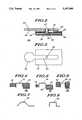
- FIG. 1is an exploded view of electrical contacts in a battery package in accordance with the invention.
- FIG. 2is a cross-sectional view of a conductive member adhered to a flexible circuit in accordance with the invention.
- FIG. 3is a plan view of the cross-sectional view shown in FIG. 2.
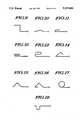
- FIGS. 4-18are cross sectional views of alternate embodiments of a portion of the conductive member.
- FIG. 19is an isometric view of electrical contacts in a battery package connected to a communications device in accordance with the invention.
- a battery package 100such as a re-chargeable battery or other similar device, consists of a housing 110 having a plurality of battery cells 120 contained within.
- the cells 120are electrically interconnected and are further connected to a flex circuit 130 or other substrate, such as a semi-flexible circuit or a rigid circuit board, by means of tabs or interconnects 122.
- the interconnect 122is shown in FIG. 1 as a metal sheet having spring fingers to hold the cells 120 against respective contact points (not shown) on the flex circuit 130, but the interconnect may alternatively consist of metal tabs welded between the individual cells 120 and to the flex circuit 130. Other methods of directly interconnecting the cells 120 and the flex circuit 130 may also be used to achieve the desired connections.
- the housing 110has walls that have one or more openings 112 therein so as to penetrate from the interior 115 of the housing to the exterior of the housing.
- the openings 112can be of any shape but are preferably circular or rectangular.
- the battery package 100is typically closed by covering the open end of the housing 110 with a cover or lid 124.
- a cross-sectional viewshows the flex circuit 130 consists of a substrate, preferably formed of a flexible insulative material such as a film of polyimide 132, having laminated to it a layer of conductive material 134, such as copper, silver filled ink, nickel, aluminum, or conductive polymers, which defines a circuit pattern.
- the conductive material 134may be attached to the polyimide 132 in a number of ways.
- a layer of adhesive 136can be interposed between the conductive material 134 and the polyimide 132, or the conductive material 134 may be attached by electroless plating, screen printing, or by sputtering a metal directly onto the polyimide 132.
- the adhesive 132is not used and adhesion of the conductive material 134 to the polyimide 132 is achieved by chemical bonding.
- the conductive material 134is typically imaged and then etched into a circuit pattern in accordance with the conventional art.
- the circuit patternmay also have other components soldered to it in order to provide appropriate functions in the battery package 100.
- componentssuch as resistors for coding the battery, thermistors for sensing the battery temperature, thermal overload switches, diodes for prevention of accidental battery discharge, capacitors, transistors, and microprocessors or other semiconductor devices may be attached to the conductive material 134. Alternate materials may be substituted for the polyimide 132, depending upon the required application.
- polyamides, polyamideimide, polyetherimides, polyesters, polyvinylchlorides, polyparabanic acids, fluoropolymers, aramides, nylons, epoxies, and various combinations of these materialsmay be employed as substrates for the flex circuit 130.
- a more rigid substratecan be substituted for the polyimide 132 if desired.
- a material known as BENDFLEX® from Rogers Corporationis a semiflexible substrate that finds applications in electronics packages. Other applications may require a rigid substrate, in which case conventional circuit board materials such as FR4, G10, reinforced polyimide, etc., may be used in place of the polyimide 132.
- each of these substratestypically also has a circuit pattern imposed thereon.
- a second conductive member 140is attached to the flex circuit 130 during the manufacture of the flex circuit.
- This conductive member 140is typically a metal such as copper, but may also be material such as nickel, nickel/silver, brass, or aluminum, and may also be further plated with a number of materials such as nickel, chrome, copper, gold, tin, solder, etc.
- the conductive member 140is affixed to the flex circuit 130 by using an adhesive 138. A portion of the conductive member 140 is bonded directly to the polyimide 132 or the conductive material 134 with the adhesive 138.
- the adhesive 138is then cured by radiation, heat, or light, as required, or it may be a thermoplastic material such as a hot-melt or a pressure-sensitive adhesive.
- the adhesive 138serves to bond the conductive member 140 to the flex circuit 130.
- the adhesive 138may cover only the polyimide 132, or it may cover only the conductive material 134, or it may cover portions of both. In any case, a judicious amount of adhesive 138 is used to secure the conductive member 140 to the flex circuit 130.
- cover coat 135 of film similar to that employed as the flex circuit base material 132may be applied over the conductive material 134.
- cover coatsare well known to those skilled in the flex circuit art. Cover coats are typically applied by adhesively bonding a film or cover coat 135 over the conductive material 134 and the polyimide 132. Openings in the cover coat 135 are formed so as to expose the conductive material 134 in strategic areas.
- a cover coat 135may also be directly applied by depositing a liquid film onto the flex circuit 130 and photoimaging the film so as to expose appropriate areas of the conductive material 134. If a cover coat 135 is employed, the adhesive 138 needed to adhere the conductive member 140 to the flex circuit 130, may also cover portions of the cover coat.
- connectionis then made between the conductive member 140 and the conductive material 134 by forming a hole 145 through the conductive member and the conductive material.
- the hole 145 shown in FIG. 2is depicted as a blind via, but may also be formed so as to penetrate completely through all of the layers of the flex circuit 130.
- the hole 145is typically created by drilling, and more than one hole per conductive member 140 may be employed.
- the hole 145may be further created by means of a laser, a punch, or a die.
- the hole 145is then filled with a conductive material such as a conductive polymer or metal filled polymer, or plated up with additional metal 147 in order to form an electrical interconnect or plated-thru hole between the conductive member 140 and the underlying conductive material 134.
- a conductive materialsuch as a conductive polymer or metal filled polymer, or plated up with additional metal 147 in order to form an electrical interconnect or plated-thru hole between the conductive member 140 and the underlying conductive material 134.
- the processes for forming the plated-thru holeare well known in the art of the printed circuit board fabrications.
- the hole 145is cleaned of debris by a de-burring operation, a plasma-cleaning, a permanganate etch, or a combination of these treatments.
- a thin layer of electroless copperis then plated into the hole 145 and also on portions of the conductive member 140 and the conductive material 134.
- Additional copper plating 147is then applied by electrochemical methods in order to build the wall of hole 145 to a suitable thickness, typically between 0.01 mm and 0.03 mm. In this way, all the electrical connections between the conductive member 140 and the conductive material 134 are formed simultaneously.
- the conductive member 140is bonded or adhered to a side of the flex circuit 130 that is opposite to the side having the conductive material 134.
- interconnection between the conductive member 140 and the conductive material 134is made by forming the hole 145 completely through the polyimide 132.
- the conductive member 140is typically thicker than the underlying conductive material 134 and is also stiffer.
- the conductive material 134is typically 0.01 to 0.07 mm thick with 0.02 to 0.05 mm being the preferred range, and it is usually very ductile.
- the conductive member 140may range from 0.05 to 1 mm in thickness, and should be stiffer than the conductive material 134 in order to retain its shape and fit properly into the housing opening 112.
- a portion 150 of the conductive member 140lies unsupported beyond the edge of the flex circuit 130. This preferred embodiment allows for later forming of the conductive member 140 to the desired configuration.
- the next stepis to form or shape the conductive member 140. If it is to be formed prior to attachment to the flex circuit 130, obviously this step would not occur at this point, but would occur prior to the adhesive bonding step.
- the conductive member 140is formed to the desired shape, for example, by etching, stamping, laser cutting, bending, die cutting, extrusion, punching, coining, or any other means necessary to achieve the desired configurations. Methods of shaping the conductive member 140 are well known in the metal working arts and are readily discernible to one with ordinary skill in the art.
- the final shape of the conductive member 140depends upon the desires of the individual designer. A typical shape is shown in a plan view in FIG. 3.
- FIGS. 4-18show cross sectional views of some possible examples that the shaped portion 150 of the conductive member 140 may assume.
- a cupmay be formed as shown in cross-sectional view in FIG. 5 where the sidewalls of the cup are essentially vertical.
- the sidewallsmay also be slanted or tapered (FIG. 7), may contain protrusions (FIG. 4, FIG. 8), or be roughened or irregularly shaped (FIG. 6) to aid in locating or retaining the portion 150 of the conductive member 140 in the housing opening 112.
- the shaping operationmay also provide features that aid in retaining the conductive member 150 in the housing opening 112, such as stakes or detents (FIG. 4).
- Other configurationssuch as an ⁇ L ⁇ -shape (FIG. 9), a contoured shape (FIG. 10), a ⁇ Dutch Bend ⁇ (FIG. 11), multiple ⁇ Dutch Bends ⁇ (FIG. 12), ⁇ S ⁇ -shapes and triangular shapes that form a spring member (FIGS. 13-16), and curled or spiral shapes (FIG. 17) can also be employed.
- this portion 150 of the conductive member 140can be a cup, a folded hat section, a ⁇ U ⁇ -shape, or a box having 3, 4, 5, or 6 sides.
- the shape of this portion 150 of the conductive member 140is typically circular when viewed from above but may be other forms such as rectangular, square, triangular, or other regular or irregular polygons. It should also be understood that these examples are by way of illustration only and are not meant to restrict the reader from implementing other configurations to achieve a similar result.
- the forming or shaping operationmodifies the configuration of the conductive member 140 in order to aid in fixturing it in the housing.
- the shaped, conductive membermay end up as a planar member or it may be shaped in multiple planes so as to form a cup, cone, rivet, flap, stud, and so forth.
- the height of the contact surface 152is significantly raised above the level of the flex circuit 130. For example, simply attaching a planar 0.37 mm thick conductive member 140 to the flex circuit 130 raises the upper contact surface 152 of the conductive member about 0.37 mm above the flex circuit.
- the formed conductive member 140When the formed conductive member 140 is inserted into the opening in the housing 112, it could lie below the plane of the exterior of the housing 110 if the housing wall thickness exceeds about 0.37 mm. Typically, most molded plastic housing walls are greater than 0.37 mm and may range as high as 2.5 mm.
- the conductive member 140By forming the conductive member 140 into a cup or similar shape, the height of the upper contact surface 152 can be raised well beyond the surface of the flex circuit 130. As can be seen in FIG. 5, the upper surface 152 of the conductive member 140 is significantly higher than the corresponding thickness of the conductive member. In this way, the shaped conductive member 140 provides for a contact surface 152 that is co-planar or even extends beyond the exterior plane of the wall of the housing 110, no matter how thick the housing wall may be.
- the unsupported portion 150may lie off the perimeter of the flex circuit 130 edge or it may alternatively lie across a hole or opening formed within the flex circuit.
- the conductive membermay be more easily formed or shaped.
- this second portion 150 of the conductive member 140may also be situated so that it lies directly over the polyimide 132. This configuration is not as amenable to being formed, but nonetheless, it may be formed or shaped if so desired.
- the flex circuit 130is then assembled into the housing 110. Additional parts, such as resistors, diodes, transistors, capacitors, switches, thermistors, and so forth, may be added, for example, by soldering.
- the flex circuit 130is connected to a plurality of battery cell 120, and this cell and flex assembly is inserted into the housing 110 with the portions 150 of the conductive members 140 fitting into the opening 112 in the housing wall. More than one conductive member 140 is used if multiple contacts are needed in the finished package 100.
- a battery package 500may be formed with electrical contacts for charging 550 and electrical contacts for connection 555 to a portable radio 570.
- contacts 150 formed by the conductive member 140may be used as contact surfaces 152 for switches, such as in popple switches, rotary switches, slide switches, and so forth. They may further be used as a spring member, as test probe points, or as heating elements if made from an alloy having high electrical resistance.
- the invention as described hereinmay find use in numerous electrical and electronic devices, such as watches, calculators, cameras, motors, computers, electronic games, battery packages, radios, and so on.
- the electrical contacts so formedare intended for use as a contact surface as distinguished from other prior art that provides plug-in terminations on flex circuits.
- the invention described hereineliminates the need to solder additional parts, such as rivets or studs, onto the flex circuit and overcomes the attendant problems associated with the conventional art, such as added material costs, added labor costs, dimensional tolerance problems, soldering operations, soldering defects and reliability problems.
Landscapes
- Engineering & Computer Science (AREA)
- Microelectronics & Electronic Packaging (AREA)
- Chemical & Material Sciences (AREA)
- Chemical Kinetics & Catalysis (AREA)
- Electrochemistry (AREA)
- General Chemical & Material Sciences (AREA)
- Connection Of Batteries Or Terminals (AREA)
Abstract
Description
This invention relates generally to electrical contacts and more specifically to electrical contacts in a housing.
It is often desirable to have electrical contacts which are mounted into a housing wall. For example, a portable, two-way radio typically includes a battery portion which has both charger contacts and contacts for connection to the radio. Various approaches are used for mounting the contacts, such as ultrasonic welding of contact carriers or the use of molded-in contacts. It is also necessary to connect the contacts to the circuit on the inside of the housing. One known approach uses rivets which are fixed to a flex circuit. Rivets, however, do not produce highly reliable electrical connections to flex circuits and require ultrasonic welding or heat staking of the contact carrier to the housing wall. It is desirable to have a contact that can be surface mounted to a flex circuit and fit directly into an opening in the housing.
U.S. Pat. No. 5,006,073 by Mennona, incorporated herein by reference, describes an electrical contact for a battery that can be snap fit into an opening in the housing. The contacts are stamped or formed from thin metal and have surfaces protruding from the walls of the contacts that include a snap feature that mates with the wall of the housing. The contacts are attached to the flex circuit by soldering. While this method of providing contacts in the housing wall provides for a low-cost, easily manufactured contact assembly, it still requires that the contacts themselves be separate piece parts and be soldered to the flex circuit in order to make the proper fit. A contacting system or scheme that could eliminate the need for additional pieces and also eliminate the soldering step would be desirable.
Briefly, according to the invention, there is provided an electrical contact for a housing, comprising a housing and a circuit assembly. The housing has at least one opening in one or more walls of the housing and the circuit assembly is situated within the housing. The circuit assembly includes a substrate material having a conductive circuit pattern on one or more sides of the substrate and an adhesive material bonded to the substrate. A conductive member is bonded to the adhesive material and is electrically connected to the conductive circuit pattern. A portion of the conductive member has a shape substantially the same as the shape of the opening in the housing. This portion is situated within the housing opening so as to form an electrical contact in the housing wall.
In another embodiment of the invention, the housing comprises a battery housing for a portable, two-way radio or other electrical device. A plurality of cells are situated within the housing. A flexible circuit is formed to interconnect the plurality of cells, and an adhesive material is bonded to a portion of the flexible circuit. A conductive member is attached to the adhesive material and electrically connected to a circuit pattern on the flex circuit. The conductive member is shaped so as to fit in or correspond to the opening in the battery housing.
FIG. 1 is an exploded view of electrical contacts in a battery package in accordance with the invention.
FIG. 2 is a cross-sectional view of a conductive member adhered to a flexible circuit in accordance with the invention.
FIG. 3 is a plan view of the cross-sectional view shown in FIG. 2.
FIGS. 4-18 are cross sectional views of alternate embodiments of a portion of the conductive member.
FIG. 19 is an isometric view of electrical contacts in a battery package connected to a communications device in accordance with the invention.
Referring to FIG. 1, abattery package 100 such as a re-chargeable battery or other similar device, consists of ahousing 110 having a plurality ofbattery cells 120 contained within. Thecells 120 are electrically interconnected and are further connected to aflex circuit 130 or other substrate, such as a semi-flexible circuit or a rigid circuit board, by means of tabs orinterconnects 122. Theinterconnect 122 is shown in FIG. 1 as a metal sheet having spring fingers to hold thecells 120 against respective contact points (not shown) on theflex circuit 130, but the interconnect may alternatively consist of metal tabs welded between theindividual cells 120 and to theflex circuit 130. Other methods of directly interconnecting thecells 120 and theflex circuit 130 may also be used to achieve the desired connections. Thehousing 110 has walls that have one ormore openings 112 therein so as to penetrate from theinterior 115 of the housing to the exterior of the housing. Theopenings 112 can be of any shape but are preferably circular or rectangular. Thebattery package 100 is typically closed by covering the open end of thehousing 110 with a cover orlid 124.
Referring now to FIG. 2, a cross-sectional view shows theflex circuit 130 consists of a substrate, preferably formed of a flexible insulative material such as a film ofpolyimide 132, having laminated to it a layer ofconductive material 134, such as copper, silver filled ink, nickel, aluminum, or conductive polymers, which defines a circuit pattern. Theconductive material 134 may be attached to thepolyimide 132 in a number of ways. For example, a layer ofadhesive 136 can be interposed between theconductive material 134 and thepolyimide 132, or theconductive material 134 may be attached by electroless plating, screen printing, or by sputtering a metal directly onto thepolyimide 132. In the latter methods, theadhesive 132 is not used and adhesion of theconductive material 134 to thepolyimide 132 is achieved by chemical bonding. Theconductive material 134 is typically imaged and then etched into a circuit pattern in accordance with the conventional art. The circuit pattern may also have other components soldered to it in order to provide appropriate functions in thebattery package 100. For example, components such as resistors for coding the battery, thermistors for sensing the battery temperature, thermal overload switches, diodes for prevention of accidental battery discharge, capacitors, transistors, and microprocessors or other semiconductor devices may be attached to theconductive material 134. Alternate materials may be substituted for thepolyimide 132, depending upon the required application. For example, polyamides, polyamideimide, polyetherimides, polyesters, polyvinylchlorides, polyparabanic acids, fluoropolymers, aramides, nylons, epoxies, and various combinations of these materials may be employed as substrates for theflex circuit 130. In addition, a more rigid substrate can be substituted for thepolyimide 132 if desired. For example, a material known as BENDFLEX® from Rogers Corporation is a semiflexible substrate that finds applications in electronics packages. Other applications may require a rigid substrate, in which case conventional circuit board materials such as FR4, G10, reinforced polyimide, etc., may be used in place of thepolyimide 132. In any event, each of these substrates typically also has a circuit pattern imposed thereon.
In order to form the electrical contact member which fits within theopening 112 of the housing wall, a secondconductive member 140 is attached to theflex circuit 130 during the manufacture of the flex circuit. Thisconductive member 140 is typically a metal such as copper, but may also be material such as nickel, nickel/silver, brass, or aluminum, and may also be further plated with a number of materials such as nickel, chrome, copper, gold, tin, solder, etc. Theconductive member 140 is affixed to theflex circuit 130 by using an adhesive 138. A portion of theconductive member 140 is bonded directly to thepolyimide 132 or theconductive material 134 with theadhesive 138. The adhesive 138 is then cured by radiation, heat, or light, as required, or it may be a thermoplastic material such as a hot-melt or a pressure-sensitive adhesive. The adhesive 138 serves to bond theconductive member 140 to theflex circuit 130. Theadhesive 138 may cover only thepolyimide 132, or it may cover only theconductive material 134, or it may cover portions of both. In any case, a judicious amount of adhesive 138 is used to secure theconductive member 140 to theflex circuit 130.
If desired, acover coat 135 of film similar to that employed as the flexcircuit base material 132 may be applied over theconductive material 134. The use of cover coats is well known to those skilled in the flex circuit art. Cover coats are typically applied by adhesively bonding a film or covercoat 135 over theconductive material 134 and thepolyimide 132. Openings in thecover coat 135 are formed so as to expose theconductive material 134 in strategic areas. Acover coat 135 may also be directly applied by depositing a liquid film onto theflex circuit 130 and photoimaging the film so as to expose appropriate areas of theconductive material 134. If acover coat 135 is employed, the adhesive 138 needed to adhere theconductive member 140 to theflex circuit 130, may also cover portions of the cover coat.
Connection is then made between theconductive member 140 and theconductive material 134 by forming ahole 145 through the conductive member and the conductive material. Thehole 145 shown in FIG. 2 is depicted as a blind via, but may also be formed so as to penetrate completely through all of the layers of theflex circuit 130. Thehole 145 is typically created by drilling, and more than one hole perconductive member 140 may be employed. Thehole 145 may be further created by means of a laser, a punch, or a die. Thehole 145 is then filled with a conductive material such as a conductive polymer or metal filled polymer, or plated up withadditional metal 147 in order to form an electrical interconnect or plated-thru hole between theconductive member 140 and the underlyingconductive material 134. The processes for forming the plated-thru hole are well known in the art of the printed circuit board fabrications. Typically, thehole 145 is cleaned of debris by a de-burring operation, a plasma-cleaning, a permanganate etch, or a combination of these treatments. A thin layer of electroless copper is then plated into thehole 145 and also on portions of theconductive member 140 and theconductive material 134. Additional copper plating 147 is then applied by electrochemical methods in order to build the wall ofhole 145 to a suitable thickness, typically between 0.01 mm and 0.03 mm. In this way, all the electrical connections between theconductive member 140 and theconductive material 134 are formed simultaneously.
In an alternate embodiment, theconductive member 140 is bonded or adhered to a side of theflex circuit 130 that is opposite to the side having theconductive material 134. In this embodiment, interconnection between theconductive member 140 and theconductive material 134 is made by forming thehole 145 completely through thepolyimide 132.
Theconductive member 140 is typically thicker than the underlyingconductive material 134 and is also stiffer. For example, theconductive material 134 is typically 0.01 to 0.07 mm thick with 0.02 to 0.05 mm being the preferred range, and it is usually very ductile. Theconductive member 140 may range from 0.05 to 1 mm in thickness, and should be stiffer than theconductive material 134 in order to retain its shape and fit properly into thehousing opening 112.
As can be seen in FIG. 2, aportion 150 of theconductive member 140 lies unsupported beyond the edge of theflex circuit 130. This preferred embodiment allows for later forming of theconductive member 140 to the desired configuration.
The next step is to form or shape theconductive member 140. If it is to be formed prior to attachment to theflex circuit 130, obviously this step would not occur at this point, but would occur prior to the adhesive bonding step. Theconductive member 140 is formed to the desired shape, for example, by etching, stamping, laser cutting, bending, die cutting, extrusion, punching, coining, or any other means necessary to achieve the desired configurations. Methods of shaping theconductive member 140 are well known in the metal working arts and are readily discernible to one with ordinary skill in the art. The final shape of theconductive member 140 depends upon the desires of the individual designer. A typical shape is shown in a plan view in FIG. 3. The shape of thisportion 150 of theconductive member 140 should substantially correspond to the shape of theopening 112 in the housing wall. Other configurations similar in nature or intent will be readily apparent to the skilled designer. For example, FIGS. 4-18 show cross sectional views of some possible examples that the shapedportion 150 of theconductive member 140 may assume. A cup may be formed as shown in cross-sectional view in FIG. 5 where the sidewalls of the cup are essentially vertical. The sidewalls may also be slanted or tapered (FIG. 7), may contain protrusions (FIG. 4, FIG. 8), or be roughened or irregularly shaped (FIG. 6) to aid in locating or retaining theportion 150 of theconductive member 140 in thehousing opening 112. The shaping operation may also provide features that aid in retaining theconductive member 150 in thehousing opening 112, such as stakes or detents (FIG. 4). Other configurations such as an `L`-shape (FIG. 9), a contoured shape (FIG. 10), a `Dutch Bend` (FIG. 11), multiple `Dutch Bends` (FIG. 12), `S`-shapes and triangular shapes that form a spring member (FIGS. 13-16), and curled or spiral shapes (FIG. 17) can also be employed. These shapes are shown here in cross section only, and the full three dimensional form of thisportion 150 of theconductive member 140 can be a cup, a folded hat section, a `U`-shape, or a box having 3, 4, 5, or 6 sides. The shape of thisportion 150 of theconductive member 140 is typically circular when viewed from above but may be other forms such as rectangular, square, triangular, or other regular or irregular polygons. It should also be understood that these examples are by way of illustration only and are not meant to restrict the reader from implementing other configurations to achieve a similar result.
The forming or shaping operation modifies the configuration of theconductive member 140 in order to aid in fixturing it in the housing. The shaped, conductive member may end up as a planar member or it may be shaped in multiple planes so as to form a cup, cone, rivet, flap, stud, and so forth. By fabricating theconductive member 140 in multiple planes, the height of thecontact surface 152 is significantly raised above the level of theflex circuit 130. For example, simply attaching a planar 0.37 mm thickconductive member 140 to theflex circuit 130 raises theupper contact surface 152 of the conductive member about 0.37 mm above the flex circuit. When the formedconductive member 140 is inserted into the opening in thehousing 112, it could lie below the plane of the exterior of thehousing 110 if the housing wall thickness exceeds about 0.37 mm. Typically, most molded plastic housing walls are greater than 0.37 mm and may range as high as 2.5 mm. By forming theconductive member 140 into a cup or similar shape, the height of theupper contact surface 152 can be raised well beyond the surface of theflex circuit 130. As can be seen in FIG. 5, theupper surface 152 of theconductive member 140 is significantly higher than the corresponding thickness of the conductive member. In this way, the shapedconductive member 140 provides for acontact surface 152 that is co-planar or even extends beyond the exterior plane of the wall of thehousing 110, no matter how thick the housing wall may be.
Theunsupported portion 150 may lie off the perimeter of theflex circuit 130 edge or it may alternatively lie across a hole or opening formed within the flex circuit. By situating aportion 150 of theconductive member 140 so that there is no underlying substrate, the conductive member may be more easily formed or shaped. Although not a preferred embodiment, thissecond portion 150 of theconductive member 140 may also be situated so that it lies directly over thepolyimide 132. This configuration is not as amenable to being formed, but nonetheless, it may be formed or shaped if so desired.
After theflex circuit 130 is fabricated, it is then assembled into thehousing 110. Additional parts, such as resistors, diodes, transistors, capacitors, switches, thermistors, and so forth, may be added, for example, by soldering. In the case of the preferred embodiment, theflex circuit 130 is connected to a plurality ofbattery cell 120, and this cell and flex assembly is inserted into thehousing 110 with theportions 150 of theconductive members 140 fitting into theopening 112 in the housing wall. More than oneconductive member 140 is used if multiple contacts are needed in thefinished package 100.
Referring now to FIG. 19, abattery package 500 may be formed with electrical contacts for charging 550 and electrical contacts forconnection 555 to aportable radio 570. Although the preferred embodiment describes abattery package 500 for an energy consuming device such as aportable radio 570, applications in other electrical apparatus may be easily envisioned. For example,contacts 150 formed by theconductive member 140 may be used as contact surfaces 152 for switches, such as in popple switches, rotary switches, slide switches, and so forth. They may further be used as a spring member, as test probe points, or as heating elements if made from an alloy having high electrical resistance. The invention as described herein may find use in numerous electrical and electronic devices, such as watches, calculators, cameras, motors, computers, electronic games, battery packages, radios, and so on.
The electrical contacts so formed are intended for use as a contact surface as distinguished from other prior art that provides plug-in terminations on flex circuits. The invention described herein eliminates the need to solder additional parts, such as rivets or studs, onto the flex circuit and overcomes the attendant problems associated with the conventional art, such as added material costs, added labor costs, dimensional tolerance problems, soldering operations, soldering defects and reliability problems.
Claims (19)
1. An assembly including an electrical contact, comprising:
a housing having multiple walls and having at least one opening in at least one of said walls; and
a circuit assembly situated within said housing, the circuit assembly comprising:
a substrate material having two major opposed faces;
a conductive circuit pattern on at least one face of said substrate material; and
a conductive member having first and second portions, said first portion bonded to said substrate with a polymeric, non-conductive adhesive and electrically connected to said conductive circuit pattern by means of a plated through hole, said second portion having a shape substantially the same as said housing opening and situated within said opening to form an electrical contact in said housing wall.
2. A housing including an electrical contact, comprising:
a housing having multiple walls and having at least one opening in at least one of said walls; and
a flexible circuit situated within said housing, the flexible circuit comprising:
a flexible film material having two opposed faces;
a conductive circuit pattern on at least one face of said flexible film material;
a polymer adhesive material bonded to at least a portion of said flexible circuit;
an integral conductive member having first and second portions, said first portion bonded to said polymer adhesive material and electrically connected to said conductive circuit pattern, said second portion having a shape substantially the same as said housing opening and situated within said opening to form an electrical contact in said housing wall; and
said conductive member formed during the fabrication of the flexible circuit.
3. The electrical contact as described in claim 2, wherein said flexible film material is selected from the group consisting of polyimides, polyamides, polyamide-imides, polyetherimides, polyesters, polyvinyl chlorides, polyparabanic acids, fluoroploymers, aramids, nylons, epoxies, and combinations thereof.
4. The electrical contact as described in claim 2, wherein said first conductive circuit pattern is copper, silver filled ink, nickel, aluminum, or a conductive polymer.
5. The electrical contact as described in claim 2, wherein said housing is a battery package housing.
6. The electrical contact as described in claim 5, further comprising a plurality of battery cells electrically connected to said flexible circuit and situated within said housing.
7. The electrical contact as described in claim 2, wherein said flexible circuit further comprises at least one covercoat.
8. The electrical contact as described in claim 7, wherein said adhesive material covers at least a portion of said covercoat and is bonded to said at least a portion of said covercoat.
9. The electrical contact as described in claim 2, wherein said flexible circuit further comprises one or more electrical components selected from the group consisting of resistors, diodes, transistors, capacitors, switches, and thermistors.
10. The electrical contact as described in claim 2, wherein said second portion of said conductive member is formed into a three dimensional shape.
11. The electrical contact as described in claim 10, wherein said second portion of said conductive member is formed so as to extend beyond said housing wall when situated within said opening.
12. The electrical contact as described in claim 10, wherein said second portion of said conductive member is formed so as to be coplanar with said housing wall when situated within said opening.
13. The electrical contact as described in claim 2, wherein said second portion of said conductive member is formed so as to provide an interference fit in said opening.
14. The electrical contact as described in claim 2, wherein said first portion of said conductive member is electrically connected to said conductive circuit pattern by means of at least one plated through hole.
15. The electrical contact as described in claim 2, wherein said adhesive material is bonded to a second face of said flexible film material, and said conductive member is bonded to said adhesive material so as to be on a side of said flexible film material opposite to said conductive circuit pattern.
16. A battery package, comprising:
a housing having multiple walls and having at least one opening in at least one of said walls;
a plurality of cells situated within said housing; and
a flexible circuit electrically connected to said plurality of cells and situated within said housing, the flexible circuit comprising:
an insulating flexible film having two opposed faces;
a copper circuit pattern on at least one face of said flexible film;
a polymer adhesive material bonded to at least a portion of said copper circuit pattern or said flexible film;
a conductive member having first and second portions, said first portion bonded to said adhesive material and electrically connected to said copper circuit pattern by means of at least one plated through hole, said second portion having a shape substantially the same as said housing opening and formed so as to substantially fit within said opening to form an electrical contact in said battery housing wall;
said conductive member being an integral part of the flexible circuit and formed during fabrication of the flexible circuit; and
one or more electrical components selected from the group consisting of resistors, diodes, transistors, capacitors, switches, and thermistors, said components soldered to said copper circuit pattern.
17. The battery package as described in claim 16, wherein said flexible film base material is selected from the group consisting of polyimides, polyamides, polyamide-imides, polyetherimides, polyesters, polyvinyl chlorides, fluoropolymers, aramids, nylons, epoxies, and combinations thereof.
18. The battery package as described in claim 16, wherein said circuit assembly further comprises at least one covercoat.
19. The battery package as described in claim 18, wherein said adhesive material covers at least a portion of said covercoat and is bonded to said at least a portion of said covercoat.
Priority Applications (1)
| Application Number | Priority Date | Filing Date | Title |
|---|---|---|---|
| US07/829,642US5197889A (en) | 1992-02-03 | 1992-02-03 | Electrical contact for battery package or similar device |
Applications Claiming Priority (1)
| Application Number | Priority Date | Filing Date | Title |
|---|---|---|---|
| US07/829,642US5197889A (en) | 1992-02-03 | 1992-02-03 | Electrical contact for battery package or similar device |
Publications (1)
| Publication Number | Publication Date |
|---|---|
| US5197889Atrue US5197889A (en) | 1993-03-30 |
Family
ID=25255105
Family Applications (1)
| Application Number | Title | Priority Date | Filing Date |
|---|---|---|---|
| US07/829,642Expired - LifetimeUS5197889A (en) | 1992-02-03 | 1992-02-03 | Electrical contact for battery package or similar device |
Country Status (1)
| Country | Link |
|---|---|
| US (1) | US5197889A (en) |
Cited By (57)
| Publication number | Priority date | Publication date | Assignee | Title |
|---|---|---|---|---|
| US5360683A (en)* | 1992-12-01 | 1994-11-01 | Nokia Mobile Phones Ltd. | Battery pack |
| WO1995007601A1 (en)* | 1993-09-07 | 1995-03-16 | Motorola, Inc. | Device with external electrical interface |
| US5472804A (en)* | 1994-12-01 | 1995-12-05 | Motorola, Inc. | Battery device with integrated circuit substrate packaging |
| GB2291278A (en)* | 1994-06-22 | 1996-01-17 | Inpin Ltd | Two part electrical connector |
| US5521022A (en)* | 1993-08-03 | 1996-05-28 | Zedel | Case for electrical batteries or accumulator cells |
| US5607791A (en)* | 1996-07-08 | 1997-03-04 | Motorola, Inc | Battery interface structure for an electrical device |
| US5607793A (en)* | 1990-11-27 | 1997-03-04 | Alexandres; Richard B. | Flexible welding board for battery pack |
| WO1999005746A1 (en)* | 1997-07-25 | 1999-02-04 | Minnesota Mining And Manufacturing Company | Thermal management system and method for a solid-state energy storing device |
| US5952815A (en)* | 1997-07-25 | 1999-09-14 | Minnesota Mining & Manufacturing Co. | Equalizer system and method for series connected energy storing devices |
| EP0898332A3 (en)* | 1997-08-20 | 1999-10-13 | Sony Corporation | Connector device |
| US6046514A (en)* | 1997-07-25 | 2000-04-04 | 3M Innovative Properties Company | Bypass apparatus and method for series connected energy storage devices |
| US6099986A (en)* | 1997-07-25 | 2000-08-08 | 3M Innovative Properties Company | In-situ short circuit protection system and method for high-energy electrochemical cells |
| US6100702A (en)* | 1997-07-25 | 2000-08-08 | 3M Innovative Properties Company | In-situ fault detection apparatus and method for an encased energy storing device |
| US6104967A (en)* | 1997-07-25 | 2000-08-15 | 3M Innovative Properties Company | Fault-tolerant battery system employing intra-battery network architecture |
| US6117584A (en)* | 1997-07-25 | 2000-09-12 | 3M Innovative Properties Company | Thermal conductor for high-energy electrochemical cells |
| US6120930A (en)* | 1997-07-25 | 2000-09-19 | 3M Innovative Properties Corporation | Rechargeable thin-film electrochemical generator |
| US6146778A (en)* | 1997-07-25 | 2000-11-14 | 3M Innovative Properties Company | Solid-state energy storage module employing integrated interconnect board |
| USD436917S1 (en) | 1999-11-17 | 2001-01-30 | Makita Corporation | Battery pack |
| WO2001018891A1 (en)* | 1999-09-08 | 2001-03-15 | Motorola Inc. | Contact system for interconnection of substrate and battery cell |
| US6235425B1 (en) | 1997-12-12 | 2001-05-22 | 3M Innovative Properties Company | Apparatus and method for treating a cathode material provided on a thin-film substrate |
| US6459176B1 (en)* | 2000-11-28 | 2002-10-01 | The United States Of America As Represented By The Secretary Of The Army | Survival radio battery adapters |
| US20030070833A1 (en)* | 2001-10-17 | 2003-04-17 | Barth Phillip W. | Extensible spiral for flex circuit |
| US6562493B2 (en)* | 1998-03-18 | 2003-05-13 | Toshiba Battery Co., Ltd. | Battery, lead member for battery connection, and battery pack using the same |
| US20050031945A1 (en)* | 2003-08-05 | 2005-02-10 | Hideyo Morita | Battery pack |
| US20050099752A1 (en)* | 2003-11-08 | 2005-05-12 | Andigilog, Inc. | Temperature sensing circuit |
| US20050099163A1 (en)* | 2003-11-08 | 2005-05-12 | Andigilog, Inc. | Temperature manager |
| US20060216589A1 (en)* | 2005-03-25 | 2006-09-28 | Front Edge Technology, Inc. | Thin film battery with protective packaging |
| US20060264108A1 (en)* | 2005-05-17 | 2006-11-23 | Masato Shimamori | Electric connector, unit for covering its connected part between two terminals, storage cell and bus bar equipped with them |
| US20070082559A1 (en)* | 2004-06-30 | 2007-04-12 | Lg Innotek Co., Ltd. | Contact spring |
| US20080176433A1 (en)* | 2007-01-22 | 2008-07-24 | Hon Hai Precision Industry Co., Ltd. | Connector adapter |
| US20080192800A1 (en)* | 2007-02-08 | 2008-08-14 | Denso Corporation | Battery condition detection apparatus |
| US20080213664A1 (en)* | 2007-03-02 | 2008-09-04 | Front Edge Technology, Inc. | Thin film battery and manufacturing method |
| US20080226979A1 (en)* | 2007-03-15 | 2008-09-18 | Youngcheol Jang | Protection circuit board for secondary battery and secondary battery using the same |
| US20080263855A1 (en)* | 2007-04-27 | 2008-10-30 | Front Edge Technology, Inc. | Thin film battery substrate cutting and fabrication process |
| US20090057136A1 (en)* | 2007-09-04 | 2009-03-05 | Front Edge Technology, Inc. | Manufacturing method for thin film battery |
| US20090136839A1 (en)* | 2007-11-28 | 2009-05-28 | Front Edge Technology, Inc. | Thin film battery comprising stacked battery cells and method |
| US20090208671A1 (en)* | 2008-02-18 | 2009-08-20 | Front Edge Technology, Inc. | Thin film battery fabrication using laser shaping |
| US20090212007A1 (en)* | 2008-02-27 | 2009-08-27 | Shinko Electric Industries Co., Ltd. | Surface treatment method |
| US20100136392A1 (en)* | 2009-10-01 | 2010-06-03 | Delphi Technologies, Inc. | Cell temperature sensing apparatus for a batttery module |
| US20100203378A1 (en)* | 2009-02-06 | 2010-08-12 | Saft Groupe Sa | Device providing electrical connection between electrochemical cells |
| US20110050159A1 (en)* | 2009-08-28 | 2011-03-03 | Front Edge Technology, Inc. | Battery charging apparatus and method |
| US20110076550A1 (en)* | 2005-03-25 | 2011-03-31 | Front Edge Technology, Inc. | Battery with protective packaging |
| US20110180291A1 (en)* | 2008-07-11 | 2011-07-28 | Robert Bosch Gmbh | Making electrical contact with a rechargeable battery having a plurality of rechargeable battery cells |
| US20120270437A1 (en)* | 2011-04-25 | 2012-10-25 | Tate Michael J | Circuit element coupling devices and methods for flexible and other circuits |
| US20130260181A1 (en)* | 2012-03-27 | 2013-10-03 | Optex Co., Ltd. | Reverse connection preventing structure for use in battery- driven object detection device |
| US8753724B2 (en) | 2012-09-26 | 2014-06-17 | Front Edge Technology Inc. | Plasma deposition on a partially formed battery through a mesh screen |
| US8864954B2 (en) | 2011-12-23 | 2014-10-21 | Front Edge Technology Inc. | Sputtering lithium-containing material with multiple targets |
| US8865340B2 (en) | 2011-10-20 | 2014-10-21 | Front Edge Technology Inc. | Thin film battery packaging formed by localized heating |
| US9077000B2 (en) | 2012-03-29 | 2015-07-07 | Front Edge Technology, Inc. | Thin film battery and localized heat treatment |
| US9257695B2 (en) | 2012-03-29 | 2016-02-09 | Front Edge Technology, Inc. | Localized heat treatment of battery component films |
| US9356320B2 (en) | 2012-10-15 | 2016-05-31 | Front Edge Technology Inc. | Lithium battery having low leakage anode |
| US9887429B2 (en) | 2011-12-21 | 2018-02-06 | Front Edge Technology Inc. | Laminated lithium battery |
| US9905895B2 (en) | 2012-09-25 | 2018-02-27 | Front Edge Technology, Inc. | Pulsed mode apparatus with mismatched battery |
| US10008739B2 (en) | 2015-02-23 | 2018-06-26 | Front Edge Technology, Inc. | Solid-state lithium battery with electrolyte |
| US10717911B2 (en) | 2015-10-09 | 2020-07-21 | Ineos Styrolution Group Gmbh | Electrically conducting thermally conductive polymer resin composition based on styrenics with balanced properties |
| USD892747S1 (en)* | 2017-10-10 | 2020-08-11 | Ebara Corporation | Electrical contact |
| US10957886B2 (en) | 2018-03-14 | 2021-03-23 | Front Edge Technology, Inc. | Battery having multilayer protective casing |
Citations (7)
| Publication number | Priority date | Publication date | Assignee | Title |
|---|---|---|---|---|
| US3553033A (en)* | 1968-08-23 | 1971-01-05 | Bright Start Ind Inc | Printed circuit lantern battery construction |
| US4117203A (en)* | 1976-11-03 | 1978-09-26 | The Gates Rubber Company | Rechargeable battery enclosure |
| US4417776A (en)* | 1980-08-12 | 1983-11-29 | Olympus Optical Co., Ltd. | Connection terminal device for electrical implements |
| US4970624A (en)* | 1990-01-22 | 1990-11-13 | Molex Incorporated | Electronic device employing a conductive adhesive |
| US5001604A (en)* | 1989-10-26 | 1991-03-19 | Lusby W Randolph | Embedded testing circuit and method for fabricating same |
| US5006073A (en)* | 1989-05-30 | 1991-04-09 | Motorola, Inc. | Snap fit contact assembly |
| US5103375A (en)* | 1990-02-05 | 1992-04-07 | Motorola, Inc. | Electronic module assembly and method of manufacture |
- 1992
- 1992-02-03USUS07/829,642patent/US5197889A/ennot_activeExpired - Lifetime
Patent Citations (7)
| Publication number | Priority date | Publication date | Assignee | Title |
|---|---|---|---|---|
| US3553033A (en)* | 1968-08-23 | 1971-01-05 | Bright Start Ind Inc | Printed circuit lantern battery construction |
| US4117203A (en)* | 1976-11-03 | 1978-09-26 | The Gates Rubber Company | Rechargeable battery enclosure |
| US4417776A (en)* | 1980-08-12 | 1983-11-29 | Olympus Optical Co., Ltd. | Connection terminal device for electrical implements |
| US5006073A (en)* | 1989-05-30 | 1991-04-09 | Motorola, Inc. | Snap fit contact assembly |
| US5001604A (en)* | 1989-10-26 | 1991-03-19 | Lusby W Randolph | Embedded testing circuit and method for fabricating same |
| US4970624A (en)* | 1990-01-22 | 1990-11-13 | Molex Incorporated | Electronic device employing a conductive adhesive |
| US5103375A (en)* | 1990-02-05 | 1992-04-07 | Motorola, Inc. | Electronic module assembly and method of manufacture |
Cited By (95)
| Publication number | Priority date | Publication date | Assignee | Title |
|---|---|---|---|---|
| US5607793A (en)* | 1990-11-27 | 1997-03-04 | Alexandres; Richard B. | Flexible welding board for battery pack |
| US5360683A (en)* | 1992-12-01 | 1994-11-01 | Nokia Mobile Phones Ltd. | Battery pack |
| US5521022A (en)* | 1993-08-03 | 1996-05-28 | Zedel | Case for electrical batteries or accumulator cells |
| WO1995007601A1 (en)* | 1993-09-07 | 1995-03-16 | Motorola, Inc. | Device with external electrical interface |
| US5427537A (en)* | 1993-09-07 | 1995-06-27 | Motorola, Inc. | Device with external interface |
| GB2291278A (en)* | 1994-06-22 | 1996-01-17 | Inpin Ltd | Two part electrical connector |
| US5472804A (en)* | 1994-12-01 | 1995-12-05 | Motorola, Inc. | Battery device with integrated circuit substrate packaging |
| WO1996017391A1 (en)* | 1994-12-01 | 1996-06-06 | Motorola Inc. | Battery device with integrated circuit substrate packaging |
| US5607791A (en)* | 1996-07-08 | 1997-03-04 | Motorola, Inc | Battery interface structure for an electrical device |
| US6641942B1 (en) | 1997-07-25 | 2003-11-04 | 3M Innovative Properties Company | Solid-state energy storage module employing integrated interconnect board |
| US6146778A (en)* | 1997-07-25 | 2000-11-14 | 3M Innovative Properties Company | Solid-state energy storage module employing integrated interconnect board |
| WO1999005746A1 (en)* | 1997-07-25 | 1999-02-04 | Minnesota Mining And Manufacturing Company | Thermal management system and method for a solid-state energy storing device |
| US6046514A (en)* | 1997-07-25 | 2000-04-04 | 3M Innovative Properties Company | Bypass apparatus and method for series connected energy storage devices |
| US6087036A (en)* | 1997-07-25 | 2000-07-11 | 3M Innovative Properties Company | Thermal management system and method for a solid-state energy storing device |
| US6099986A (en)* | 1997-07-25 | 2000-08-08 | 3M Innovative Properties Company | In-situ short circuit protection system and method for high-energy electrochemical cells |
| US6100702A (en)* | 1997-07-25 | 2000-08-08 | 3M Innovative Properties Company | In-situ fault detection apparatus and method for an encased energy storing device |
| US6104967A (en)* | 1997-07-25 | 2000-08-15 | 3M Innovative Properties Company | Fault-tolerant battery system employing intra-battery network architecture |
| US6117584A (en)* | 1997-07-25 | 2000-09-12 | 3M Innovative Properties Company | Thermal conductor for high-energy electrochemical cells |
| US6797018B2 (en) | 1997-07-25 | 2004-09-28 | 3M Innovative Properties Company | Solid-state energy storage module employing integrated interconnect board |
| US6120930A (en)* | 1997-07-25 | 2000-09-19 | 3M Innovative Properties Corporation | Rechargeable thin-film electrochemical generator |
| US5952815A (en)* | 1997-07-25 | 1999-09-14 | Minnesota Mining & Manufacturing Co. | Equalizer system and method for series connected energy storing devices |
| US6569559B1 (en) | 1997-07-25 | 2003-05-27 | 3M Innovative Properties Company | Method for transferring thermal energy and electrical current in thin-film electrochemical cells |
| US6548206B1 (en) | 1997-07-25 | 2003-04-15 | 3M Innovative Properties Company | In-situ short-circuit protection system and method for high-energy electrochemical cells |
| US6116932A (en)* | 1997-08-20 | 2000-09-12 | Sony Corporation | Connector device |
| EP0898332A3 (en)* | 1997-08-20 | 1999-10-13 | Sony Corporation | Connector device |
| US6235425B1 (en) | 1997-12-12 | 2001-05-22 | 3M Innovative Properties Company | Apparatus and method for treating a cathode material provided on a thin-film substrate |
| US6517591B2 (en) | 1997-12-12 | 2003-02-11 | 3M Innovative Properties Company | Apparatus and method for treating a cathode material provided on a thin-film substrate |
| US6562493B2 (en)* | 1998-03-18 | 2003-05-13 | Toshiba Battery Co., Ltd. | Battery, lead member for battery connection, and battery pack using the same |
| WO2001018891A1 (en)* | 1999-09-08 | 2001-03-15 | Motorola Inc. | Contact system for interconnection of substrate and battery cell |
| USD436917S1 (en) | 1999-11-17 | 2001-01-30 | Makita Corporation | Battery pack |
| US6459176B1 (en)* | 2000-11-28 | 2002-10-01 | The United States Of America As Represented By The Secretary Of The Army | Survival radio battery adapters |
| US20030070833A1 (en)* | 2001-10-17 | 2003-04-17 | Barth Phillip W. | Extensible spiral for flex circuit |
| US7275562B2 (en) | 2001-10-17 | 2007-10-02 | Agilent Technologies, Inc. | Extensible spiral for flex circuit |
| DE102004037836B4 (en) | 2003-08-05 | 2020-01-23 | Sanyo Electric Co., Ltd. | battery pack |
| US7678493B2 (en)* | 2003-08-05 | 2010-03-16 | Sanyo Electric Co., Ltd. | Battery pack |
| US20050031945A1 (en)* | 2003-08-05 | 2005-02-10 | Hideyo Morita | Battery pack |
| US7857510B2 (en) | 2003-11-08 | 2010-12-28 | Carl F Liepold | Temperature sensing circuit |
| US20050099752A1 (en)* | 2003-11-08 | 2005-05-12 | Andigilog, Inc. | Temperature sensing circuit |
| US20050099163A1 (en)* | 2003-11-08 | 2005-05-12 | Andigilog, Inc. | Temperature manager |
| US20070082559A1 (en)* | 2004-06-30 | 2007-04-12 | Lg Innotek Co., Ltd. | Contact spring |
| US7438559B2 (en)* | 2004-06-30 | 2008-10-21 | Lg Innotek Co., Ltd. | Contact spring |
| US7846579B2 (en) | 2005-03-25 | 2010-12-07 | Victor Krasnov | Thin film battery with protective packaging |
| US8475955B2 (en) | 2005-03-25 | 2013-07-02 | Front Edge Technology, Inc. | Thin film battery with electrical connector connecting battery cells |
| US20100227214A1 (en)* | 2005-03-25 | 2010-09-09 | Front Edge Technology, Inc. | Thin film battery with protective packaging |
| US20110076550A1 (en)* | 2005-03-25 | 2011-03-31 | Front Edge Technology, Inc. | Battery with protective packaging |
| US8168322B2 (en) | 2005-03-25 | 2012-05-01 | Front Edge Technology, Inc. | Thin film battery with protective packaging |
| US8679674B2 (en) | 2005-03-25 | 2014-03-25 | Front Edge Technology, Inc. | Battery with protective packaging |
| US20060216589A1 (en)* | 2005-03-25 | 2006-09-28 | Front Edge Technology, Inc. | Thin film battery with protective packaging |
| US7381093B2 (en)* | 2005-05-17 | 2008-06-03 | Ykk Corporation | Covered snap-fit terminals for connecting storage cells together |
| US20060264108A1 (en)* | 2005-05-17 | 2006-11-23 | Masato Shimamori | Electric connector, unit for covering its connected part between two terminals, storage cell and bus bar equipped with them |
| US20080176433A1 (en)* | 2007-01-22 | 2008-07-24 | Hon Hai Precision Industry Co., Ltd. | Connector adapter |
| US7896543B2 (en)* | 2007-02-08 | 2011-03-01 | Denso Corporation | Battery condition detection apparatus |
| US20080192800A1 (en)* | 2007-02-08 | 2008-08-14 | Denso Corporation | Battery condition detection apparatus |
| US20080213664A1 (en)* | 2007-03-02 | 2008-09-04 | Front Edge Technology, Inc. | Thin film battery and manufacturing method |
| US7862927B2 (en) | 2007-03-02 | 2011-01-04 | Front Edge Technology | Thin film battery and manufacturing method |
| US8492013B2 (en) | 2007-03-15 | 2013-07-23 | Samsung Sdi Co., Ltd. | Protection circuit board for secondary battery and secondary battery using the same |
| US20110111265A1 (en)* | 2007-03-15 | 2011-05-12 | Samsung Sdi Co.,Ltd. | Protection circuit board for secondary battery and secondary battery using the same |
| EP1970722A3 (en)* | 2007-03-15 | 2008-12-31 | Samsung SDI Co., Ltd. | Protection Circuit Board for Secondary Battery |
| US7898814B2 (en) | 2007-03-15 | 2011-03-01 | Samsung Sdi Co., Ltd. | Protection circuit board for secondary battery and secondary battery using the same |
| US20080226979A1 (en)* | 2007-03-15 | 2008-09-18 | Youngcheol Jang | Protection circuit board for secondary battery and secondary battery using the same |
| US20080263855A1 (en)* | 2007-04-27 | 2008-10-30 | Front Edge Technology, Inc. | Thin film battery substrate cutting and fabrication process |
| US7862627B2 (en) | 2007-04-27 | 2011-01-04 | Front Edge Technology, Inc. | Thin film battery substrate cutting and fabrication process |
| US8728176B2 (en) | 2007-04-27 | 2014-05-20 | Front Edge Technology, Inc. | Pulsed laser cutting of thin film battery |
| US20110094094A1 (en)* | 2007-04-27 | 2011-04-28 | Front Edge Technology, Inc. | Pulsed laser cutting of thin film battery |
| US8628645B2 (en) | 2007-09-04 | 2014-01-14 | Front Edge Technology, Inc. | Manufacturing method for thin film battery |
| US20090057136A1 (en)* | 2007-09-04 | 2009-03-05 | Front Edge Technology, Inc. | Manufacturing method for thin film battery |
| US20090136839A1 (en)* | 2007-11-28 | 2009-05-28 | Front Edge Technology, Inc. | Thin film battery comprising stacked battery cells and method |
| US8870974B2 (en) | 2008-02-18 | 2014-10-28 | Front Edge Technology, Inc. | Thin film battery fabrication using laser shaping |
| US20090208671A1 (en)* | 2008-02-18 | 2009-08-20 | Front Edge Technology, Inc. | Thin film battery fabrication using laser shaping |
| US20090212007A1 (en)* | 2008-02-27 | 2009-08-27 | Shinko Electric Industries Co., Ltd. | Surface treatment method |
| US20110180291A1 (en)* | 2008-07-11 | 2011-07-28 | Robert Bosch Gmbh | Making electrical contact with a rechargeable battery having a plurality of rechargeable battery cells |
| US8869913B2 (en)* | 2008-07-11 | 2014-10-28 | Robert Bosch Gmbh | Making electrical contact with a rechargeable battery having a plurality of rechargeable battery cells |
| FR2942078A1 (en)* | 2009-02-06 | 2010-08-13 | Saft Groupe Sa | DEVICE FOR ELECTRICAL CONNECTION BETWEEN ELECTROCHEMICAL GENERATORS. |
| US20100203378A1 (en)* | 2009-02-06 | 2010-08-12 | Saft Groupe Sa | Device providing electrical connection between electrochemical cells |
| EP2224515A1 (en)* | 2009-02-06 | 2010-09-01 | Saft Groupe S.A. | Device for electrical connection between electrochemical generators |
| US8502494B2 (en) | 2009-08-28 | 2013-08-06 | Front Edge Technology, Inc. | Battery charging apparatus and method |
| US20110050159A1 (en)* | 2009-08-28 | 2011-03-03 | Front Edge Technology, Inc. | Battery charging apparatus and method |
| US8287185B2 (en)* | 2009-10-01 | 2012-10-16 | Delphi Technologies, Inc. | Cell temperature sensing apparatus for a battery module |
| US20100136392A1 (en)* | 2009-10-01 | 2010-06-03 | Delphi Technologies, Inc. | Cell temperature sensing apparatus for a batttery module |
| US8460026B2 (en)* | 2011-04-25 | 2013-06-11 | Soligic, Inc. | Circuit element coupling devices and methods for flexible and other circuits |
| US20120270437A1 (en)* | 2011-04-25 | 2012-10-25 | Tate Michael J | Circuit element coupling devices and methods for flexible and other circuits |
| US8865340B2 (en) | 2011-10-20 | 2014-10-21 | Front Edge Technology Inc. | Thin film battery packaging formed by localized heating |
| US9887429B2 (en) | 2011-12-21 | 2018-02-06 | Front Edge Technology Inc. | Laminated lithium battery |
| US8864954B2 (en) | 2011-12-23 | 2014-10-21 | Front Edge Technology Inc. | Sputtering lithium-containing material with multiple targets |
| US20130260181A1 (en)* | 2012-03-27 | 2013-10-03 | Optex Co., Ltd. | Reverse connection preventing structure for use in battery- driven object detection device |
| US9059458B2 (en)* | 2012-03-27 | 2015-06-16 | Optex Co., Ltd. | Reverse connection preventing structure for use in battery-driven object detection device |
| US9257695B2 (en) | 2012-03-29 | 2016-02-09 | Front Edge Technology, Inc. | Localized heat treatment of battery component films |
| US9077000B2 (en) | 2012-03-29 | 2015-07-07 | Front Edge Technology, Inc. | Thin film battery and localized heat treatment |
| US9905895B2 (en) | 2012-09-25 | 2018-02-27 | Front Edge Technology, Inc. | Pulsed mode apparatus with mismatched battery |
| US8753724B2 (en) | 2012-09-26 | 2014-06-17 | Front Edge Technology Inc. | Plasma deposition on a partially formed battery through a mesh screen |
| US9356320B2 (en) | 2012-10-15 | 2016-05-31 | Front Edge Technology Inc. | Lithium battery having low leakage anode |
| US10008739B2 (en) | 2015-02-23 | 2018-06-26 | Front Edge Technology, Inc. | Solid-state lithium battery with electrolyte |
| US10717911B2 (en) | 2015-10-09 | 2020-07-21 | Ineos Styrolution Group Gmbh | Electrically conducting thermally conductive polymer resin composition based on styrenics with balanced properties |
| USD892747S1 (en)* | 2017-10-10 | 2020-08-11 | Ebara Corporation | Electrical contact |
| US10957886B2 (en) | 2018-03-14 | 2021-03-23 | Front Edge Technology, Inc. | Battery having multilayer protective casing |
Similar Documents
| Publication | Publication Date | Title |
|---|---|---|
| US5197889A (en) | Electrical contact for battery package or similar device | |
| KR100327004B1 (en) | Electrical connections with deformable contacts | |
| US4026011A (en) | Flexible circuit assembly | |
| EP0197148B1 (en) | Printed-circuit board for mounting electronic element and method of manufacture thereof | |
| US6208521B1 (en) | Film carrier and laminate type mounting structure using same | |
| EP0065425B1 (en) | Hybrid integrated circuit component and printed circuit board mounting said component | |
| US5038251A (en) | Electronic apparatus and a method for manufacturing the same | |
| US4920019A (en) | Battery pack assembly having a circuit board | |
| US6490168B1 (en) | Interconnection of circuit substrates on different planes in electronic module | |
| US5223676A (en) | Composite circuit board having means to suppress heat diffusion and manufacturing method of the same | |
| JP2007508681A (en) | Apparatus and method for interconnecting battery cells in a battery pack | |
| EP0478879B1 (en) | A system of interconnecting electrical elements having differing bonding requirements for mounting said elements to a printed circuit board | |
| US4599486A (en) | High capacitance bus bar including multilayer ceramic capacitors | |
| EP0748152B1 (en) | Method for mounting an electronic component on a wiring substrate and an electronic device using this mounting method | |
| JP2784522B2 (en) | Electronic component mounting substrate and method of manufacturing the same | |
| CN112040629B (en) | Circuit board and manufacturing method thereof | |
| US5625224A (en) | Method and apparatus for an integrated circuit chip carrier having improved mounting pad density | |
| JPH0143473B2 (en) | ||
| JP2784524B2 (en) | Multilayer electronic component mounting substrate and method of manufacturing the same | |
| KR100774894B1 (en) | Semiconductor device | |
| US4691188A (en) | Circuit board | |
| US5761792A (en) | Method for making a battery pack | |
| JPH09331143A (en) | Electronic component mounting method on flexible wiring board | |
| EP0488581B1 (en) | Flexible welding board for battery pack | |
| US20040074669A1 (en) | Circuit board and method of making circuit board |
Legal Events
| Date | Code | Title | Description |
|---|---|---|---|
| AS | Assignment | Owner name:MOTOROLA, INC., A CORP. OF DE, ILLINOIS Free format text:ASSIGNMENT OF ASSIGNORS INTEREST.;ASSIGNORS:RIZZO, MATTHEW;BRESIN, MARK S.;REEL/FRAME:006001/0930 Effective date:19920131 | |
| STCF | Information on status: patent grant | Free format text:PATENTED CASE | |
| FPAY | Fee payment | Year of fee payment:4 | |
| FPAY | Fee payment | Year of fee payment:8 | |
| FEPP | Fee payment procedure | Free format text:PAYOR NUMBER ASSIGNED (ORIGINAL EVENT CODE: ASPN); ENTITY STATUS OF PATENT OWNER: LARGE ENTITY | |
| FPAY | Fee payment | Year of fee payment:12 | |
| AS | Assignment | Owner name:MOTOROLA MOBILITY, INC, ILLINOIS Free format text:ASSIGNMENT OF ASSIGNORS INTEREST;ASSIGNOR:MOTOROLA, INC;REEL/FRAME:025673/0558 Effective date:20100731 |