US5193131A - Optoelectronic device with an integrated optical guide and photodetector - Google Patents
Optoelectronic device with an integrated optical guide and photodetectorDownload PDFInfo
- Publication number
- US5193131A US5193131AUS07/875,018US87501892AUS5193131AUS 5193131 AUS5193131 AUS 5193131AUS 87501892 AUS87501892 AUS 87501892AUS 5193131 AUS5193131 AUS 5193131A
- Authority
- US
- United States
- Prior art keywords
- layer
- guide
- index
- partial reflecting
- cic
- Prior art date
- Legal status (The legal status is an assumption and is not a legal conclusion. Google has not performed a legal analysis and makes no representation as to the accuracy of the status listed.)
- Expired - Lifetime
Links
- 230000003287optical effectEffects0.000titleclaimsabstractdescription18
- 230000005693optoelectronicsEffects0.000titleclaimsabstractdescription7
- 238000010521absorption reactionMethods0.000claimsdescription38
- 239000000463materialSubstances0.000claimsdescription28
- 239000002250absorbentSubstances0.000claimsdescription23
- 230000002745absorbentEffects0.000claimsdescription22
- 239000000758substrateSubstances0.000claimsdescription7
- 229910000530Gallium indium arsenideInorganic materials0.000claimsdescription6
- 230000005855radiationEffects0.000claimsdescription2
- 239000004065semiconductorSubstances0.000claimsdescription2
- 229910002059quaternary alloyInorganic materials0.000claims3
- 239000012080ambient airSubstances0.000claims1
- 229910002058ternary alloyInorganic materials0.000claims1
- 238000000407epitaxyMethods0.000description6
- 238000005530etchingMethods0.000description5
- 230000008878couplingEffects0.000description4
- 238000010168coupling processMethods0.000description4
- 238000005859coupling reactionMethods0.000description4
- 238000001514detection methodMethods0.000description4
- 238000004519manufacturing processMethods0.000description4
- 239000002800charge carrierSubstances0.000description3
- 238000000151depositionMethods0.000description3
- 230000008021depositionEffects0.000description3
- 238000001451molecular beam epitaxyMethods0.000description3
- 239000011358absorbing materialSubstances0.000description2
- 230000010354integrationEffects0.000description2
- 238000004943liquid phase epitaxyMethods0.000description2
- 238000000034methodMethods0.000description2
- 238000002310reflectometryMethods0.000description2
- NINIDFKCEFEMDL-UHFFFAOYSA-NSulfurChemical compound[S]NINIDFKCEFEMDL-UHFFFAOYSA-N0.000description1
- 239000005864SulphurSubstances0.000description1
- 230000006978adaptationEffects0.000description1
- 238000004458analytical methodMethods0.000description1
- 238000004364calculation methodMethods0.000description1
- 239000000969carrierSubstances0.000description1
- 230000001419dependent effectEffects0.000description1
- 238000009792diffusion processMethods0.000description1
- 230000005684electric fieldEffects0.000description1
- 239000002184metalSubstances0.000description1
- 230000001902propagating effectEffects0.000description1
- 239000000523sampleSubstances0.000description1
- 238000005070samplingMethods0.000description1
- 238000000926separation methodMethods0.000description1
- 238000004904shorteningMethods0.000description1
Images


Classifications
- G—PHYSICS
- G02—OPTICS
- G02B—OPTICAL ELEMENTS, SYSTEMS OR APPARATUS
- G02B6/00—Light guides; Structural details of arrangements comprising light guides and other optical elements, e.g. couplings
- G02B6/24—Coupling light guides
- G02B6/42—Coupling light guides with opto-electronic elements
Definitions
- the present inventionrelates to an optoelectronic device with an integrated optical guide and photodetector. It is used in optoelectronics and in particular optical telecommunications, where the device according to the invention can constitute the optical receiver of a heterodyne reception circuit.
- the device according to the inventioncan also be used in optical interconnections between high speed electronic chips with a high degree of integration, or between computers, or within computers.
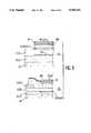
- FIG. 1An optoelectronic device with an integrated optical guide and photodetector is shown in FIG. 1, with three slightly different embodiments.
- the devicecomprises, on a semiconductor substrate S and in succession: a first lower confinement layer CiC made from a first material having a first index (n1), a second guide layer CG made from a second material and having a second index (n2) higher than the first (n1) and a third upper confinement layer CsC made from a third material with a third index (n3) lower than that of the second material (n2).
- a first lower confinement layer CiCmade from a first material having a first index (n1)
- a second guide layer CGmade from a second material and having a second index (n2) higher than the first (n1)
- a third upper confinement layer CsCmade from a third material with a third index (n3) lower than that of the second material (n2).
- This structureis completed by a detector D positioned at different locations as a function of the embodiment, either in the lower part of the substrate (part a in FIG. 1), a mirror M at 45° reflecting the light from the guide layer downwards, or at the end of the guide layer (part b), or above the guide layer (part c) for an evanescent wave operation.
- the device according to the inventionrelates to the third embodiment, i.e. that which will be described in greater detail hereinafter.
- An integrated detector--guide device with coupling by evanescent waveis e.g. described in the article by R. J. DERI et al entitled: "Integrated Waveguide/Photodiodes with Vertical Impedance Matching", published in “Proceedings of the 1989 IEDM", Washington D. C., December, 1989.
- part ais a plan view
- part ba section at the entrance of the detector
- part ca section at the exit of the detector.
- the circular or elongated spot FLrepresents a section of the light beam propagating in the device.
- the least absorbing deviceshave, between the guide layer CG and the absorbent material Ab, an upper confinement layer CsC in the form of a guide for maintaining the transverse confinement on an approximately 3 ⁇ m band (cf. FIG. 3).
- the separation between the guide and the absorbentreduces the absorption by evaescence.
- detector widthi.e. the dimension perpendicular to the guide (dimension visible in parts b and c of FIGS. 2 and 3). It is possible to make a distinction between two detector types, depending on whether the width is significant (FIG. 2) or not (FIG. 3).
- the wide detectorsare used for avoiding lateral losses due to the natural widening of the beam. For example, a width of 32 ⁇ m is used by R. J. DERI et al, referred to hereinbefore, for 5 to 7 ⁇ m guide widths.
- the beamwidens and passes from 7 ⁇ m at the entrance to the detector to 15 ⁇ m at the exit, as shown in parts b and c of FIG. 2.
- the detector widthwould have to exceed 20 ⁇ m to bring about total absorption.
- R. J. DERI et alpropose shortening the absorption length by introducing an anti-reflection layer between the guide layer CG and the absorbent Ab.
- the index and thickness of this layermust be chosen so as to reduce the reflection at the interface between the guide layer and the absorbent layer. Taking 3.162 for the index of the guide and 3.53 for the index of the absorbent, a good index choice consists of taking an intermediate value of e.g. 3.22.
- the maximum absorption valuecorresponds to an anti-reflection layer thickness between 0.5 and 0.6 ⁇ m.
- the value chosen by R. J. DERI et alis 0.55 ⁇ m.
- the structurethen has the appearance shown in FIG. 4, where the anti-reflection layer carries the reference CaR.
- the object of the inventionis to obviate all these disadvantages associated with the varying absorption and the varying detection speed.
- the inventionproposes a device with an integrated optical guide and photodetector designed to lead to a complete absorption of the light and to have a reduced response time.
- a partial reflecting layerinserted between the lower confinement layer and the guide layer.
- Said layeris placed beneath the absorbent layer. It is made from a material having an index (n5), whose value is outside the range defined by the first index (n1) of the lower confinement layer and the second index (n2) of the guide layer.
- the index of the partial reflecting layeris preferably below the index of the lower confinement layer. In the case where the index is higher than that of the guide layer, said layer becomes guiding and reduces the absorption.
- the partial reflecting layeris located in the guide and in the lower part thereof.
- the partial reflecting layeris located in the lower confinement layer and in the upper part thereof.
- FIG. 4already described, a known device with an anti-reflection adaptation layer.
- FIG. 5shows a device according to the invention, in plan view in part a and in section in part b.
- the devicecomprises a partial reflecting layer CR located at the interface between the guide layer CG and the lower confinement layer CiC.
- the layer CRcan be n + doped.
- the absorbent Abpartly p + (Zn) over a thickness of approximately 0.5 ⁇ m on the surface, is covered with a metal layer CM, which constitutes the electrical output of the detector.
- the inventionis applicable both to cases of guide layers with a limited thickness and to those having a significant thickness.
- the differenceessentially relates to the absorption lengths.
- a 90% absorption on 50 ⁇ mis related to a 0.9 ⁇ m thick guide layer and R. J. DERI et al describe a 190 ⁇ m long detector for the same absorption with a 3.5 ⁇ m thick guide.
- the absorption lengthis shorter on a guide of limited thickness.
- Thick monomode guidesare obtained by using a small index difference between that of the guide layer and that of the confinement layers.
- useis made in this case with a propagation at e.g. a wavelength of 1.5 ⁇ m of an InGaAsP layer of index 3.38 and for the lower confinement layer an InGaAsP layer of index 3.37 (slightly lower).
- Airis used as the upper confinement material.
- the guide layerIn order to be monomodal, the guide layer must have a thickness of approximately 3 ⁇ m.
- the guides of limited thicknessare obtained by using a large index difference between that of the guide layer and that of the confinement layers.
- the guide layeris e.g. constituted by an InGaAsP quaternary layer which, for a certain concentration of these components, has an index of 3.46. Use is made in the case of the confinement layers of InGaAsP layers with an index of 3.354.
- the guideis monomodal for a thickness below 0.9 ⁇ m.
- the quaternary GaInAs materialwill be used as the detection absorbing material and is placed above the guide. To permit this positioning, in the case of small thicknesses, the upper confinement layer is etched to the guide.
- the reflecting layer CRis located in the lower part of the guide layer CG.
- the reflecting layer CRis located in the upper part of the lower confinement layer CiC.
- the reflecting layercan either be positioned as in a, or as in b, for both embodiments.
- the reflecting layer CRmust have an index below that of the confinement layers.
- a guide made from quaternary GaInAsPe.g. with an index close to 3.38 and 3.37, i.e. having a forbidden band around 1.3 ⁇ m for a guide thickness of 3 ⁇ m.
- the reflection at the interfaceis in this case higher than the value assumed without said layer.
- the lightis returned towards the absorption layer Ab.
- the action of the reflecting layer CRcan be reinforced by the addition of an anti-reflection layer placed above the guide layer beneath the absorbent (as described by R. J. DERI et al).
- Said layer CaR(n + ) on part a of FIG. 6makes it possible to reduce the reflectivity of the guide-absorbent interface and therefore facilitate the passage of light into the absorbing material.
- the combination of said anti-reflection layer and the reflecting layer according to the inventionmakes it possible to reduce the absorption length by approximately five times.
- the absorption for the 0.9 ⁇ m thick guideis twice higher with the reflecting layer. Without said layer and with evanescent coupling, the absorption is approximately 1000 cm -1 . It reaches 2000 -1 for a thickness exceeding approximately 0.4 ⁇ m for the InP layer of index 3.17 (below the index of the lower confinement layer of 3.38).
- the thicknessis not critical, the absorption remaining constant in said zone, which facilitates the production of the structure.
- a very short absorption length of 23 ⁇ mis obtained for 99% absorption in place of 46 ⁇ m.
- the reflecting layerreduces the natural widening of the beam by reducing the absorption length.
- the detection lengthis 250 ⁇ m and its width, taking account of the widening, is min. 30 ⁇ m.
- These valuesare reduced to 135 ⁇ m for the length and 15 ⁇ m for the width using a reflecting layer according to the invention, which increases the absorption.
- a reduction factor of 4is obtained for the surface of the detector for 99% absorption without an upper anti-reflection layer.
- detectorscan be used in the present invention, namely the PIN photodiode, the photoconductor and the M.S.M. photodetector.
- the two latterhave a surface electrode configuration and the former a volume configuration.
- the p contactis obtained by diffusion and the n + contact by doping during the epitaxy of the reflecting layer (cf. part b of FIG. 5).
- the intrinsic zoneis solely constituted by absorbent material (and the guide layer, if the anti-reflection layer is not used), which permits a fast transit of the charge carriers.
- the contact on the n + layeris obtained by making, in the vicinity of the detector, a hole up to the n + doped layer.
- the PIN-guide configurationwith a thick guide layer and a 135 ⁇ 15 ⁇ m detecting surface, a n + doped anti-reflection layer and a reflecting layer beneath the guide, permits an operation at a frequency exceeding 20 GHz for an absorption of 99% with a ternary thickness of 1.7 ⁇ m.
- the inventionis applicable to all materials making it possible to integrate an optical guide and a detector.
- the only condition to be respectedis that the reflecting layer has an index below that of the confinement layer.
- the thickness of the reflecting layerwhich is most suitable for increasing in the optimum possible way the reflectivity at the interface between the guide layer and the lower confinement layer.
- the reflecting layeris a ribbon, whose length is substantially that of the detector and whose width is dependent on the expansion of the beam.
- the ribbon widthcan exceed said value if the structure requires a widening between the guide and the detector in order to reduce the optical intensity per surface unit reaching the detector. The intensity must be reduced to prevent the saturation of the detector, particularly in structures using guides of limited thickness.
- the production of the device according to the inventionis subdivided into three stages, firstly the production of the ribbon-like reflecting layer on the substrate, then the deposition of a guide layer and the anti-reflection layer and finally the deposition of an epitaxied absorbent material layer for producing the detector.
- the lower confinement layercan be of GaInAsP. It is deposited on an InP substrate with, in the detecting zone, an InP reflecting layer with a thickness exceeding approximately 0.4 ⁇ m. This layer is followed by a quaternary, 3 ⁇ m thick GaInAsP layer.
- the GaInAsP material, with a forbidden band of 1.3 ⁇ mcan prove suitable. It will serve as a guide as a result of its higher index.
- a GaInAsP anti-reflection layer with an index intermediate between that of the absorbent and that of the guideis placed above the guide layer.
- an absorbent GaInAs layeris deposited, followed by a zinc-doped GaInAs layer.
- the GaInAsis etched by the dry or wet method, as is the anti-reflection layer. This etching makes it possible to produce a rectangular mesa having dimensions greater than that of the detector.
- the photoconductive PIN diodeis produced as a result of the upper GaInAs layer for the p + contact and by sulphur doping of the anti-reflection layer for the n + contact.
- the intermediate zone(between n + and p + ) is the intrinsic zone, which must be reduced to a minimum to reduce the transit time of the carriers.
- the n + doped layeris positioned level with the substrate and the intrinsic zone contains the lower confinement layer, the guide layer and the absorbent, which considerably increases the transit time of the charge carriers.
- the thickness of the absorbentmust exceed 1 ⁇ m to be effective. Between 1 and 2 ⁇ m intrinsic zone, the operating frequencies are between approximately 20 and 50 GHz.
- the electrodesare located on the surface and it is no longer necessary to dope the anti-reflection layer and add a p + doped layer.
- the guideis a ribbon produced by etching the 3 ⁇ m thick InP guide layer to permit the lateral confinement.
- the guidesare produced by the deposition of a guide layer and an upper confinement layer on the structure containing the reflecting layer and by etching the upper confinement layer.
- the etching of the guideis carried out at the same time as the etching at the guide end of the confinement layer in order to position the detector.
- the thickness of the upper confinement layermust be as small as possible in order to facilitate repeat epitaxy on the step.
- a minimum choice of 0.5 ⁇ m InPis imposed for avoiding absorption before the beam reaches the detector.
- the guide layeris not etched.
- the second stageconsists of producing an epitaxy repeat of the absorbent material constituting the detector, either by metalorganic epitaxy (MOE), or by molecular beam epitaxy (MBE).
- MOEmetalorganic epitaxy
- MBEmolecular beam epitaxy
- the detectorTo limit current leaks, the detector must be placed on a planar surface. For this purpose, it must be approximately 1 ⁇ m from the guide end step. The length of this disturbed intermediate zone is minimized by the use of evanescent coupling which facilitates the planarization of the repeat due to a smaller guide end step. In this case, it is appropriate, in order to avoid lags between absorption and detection, to place the reflecting layer in the detecting zone in order to increase absorption at the detector.
- MOE or MBEfor epitaxy repeat, although non-planar, as opposed to liquid phase epitaxy (LPE).
- LPEliquid phase epitaxy
- the device according to the inventioncan be used as an optical probe for sampling part of an optical beam travelling in the guide.
- the detector lengthis then reduced to a value below that which would lead to a total absorption.
- the optical beamstill remains guided by the reflecting layer below the guide and can therefore be used beyond this in the remainder of the circuit.
- the reflecting layer CRcan be constituted by a plurality of layers having different indices.
Landscapes
- Physics & Mathematics (AREA)
- General Physics & Mathematics (AREA)
- Optics & Photonics (AREA)
- Light Receiving Elements (AREA)
- Optical Integrated Circuits (AREA)
- Optical Couplings Of Light Guides (AREA)
Abstract
Description
Claims (12)
Applications Claiming Priority (2)
| Application Number | Priority Date | Filing Date | Title |
|---|---|---|---|
| FR9105299AFR2676126B1 (en) | 1991-04-30 | 1991-04-30 | OPTOELECTRONIC DEVICE WITH INTEGRATED OPTICAL GUIDE AND PHOTODETECTOR. |
| FR9105299 | 1991-04-30 |
Publications (1)
| Publication Number | Publication Date |
|---|---|
| US5193131Atrue US5193131A (en) | 1993-03-09 |
Family
ID=9412389
Family Applications (1)
| Application Number | Title | Priority Date | Filing Date |
|---|---|---|---|
| US07/875,018Expired - LifetimeUS5193131A (en) | 1991-04-30 | 1992-04-28 | Optoelectronic device with an integrated optical guide and photodetector |
Country Status (5)
| Country | Link |
|---|---|
| US (1) | US5193131A (en) |
| EP (1) | EP0511913B1 (en) |
| JP (1) | JP3221916B2 (en) |
| DE (1) | DE69217701T2 (en) |
| FR (1) | FR2676126B1 (en) |
Cited By (30)
| Publication number | Priority date | Publication date | Assignee | Title |
|---|---|---|---|---|
| US5373570A (en)* | 1992-07-21 | 1994-12-13 | France Telecom | Process for forming a structure with integrated optical waveguide and mirror, and structure obtained |
| US5513288A (en)* | 1992-06-15 | 1996-04-30 | Robert Bosch Gmbh | Optical polymer element for coupling photoelements onto integrated-optical circuits |
| US5523557A (en)* | 1994-04-26 | 1996-06-04 | France Telecom | Optoelectronic device integrating a light guide and a photodetector having two diodes arranged side by side on a semiconductor substrate |
| FR2761813A1 (en)* | 1997-04-08 | 1998-10-09 | Thomson Csf | MULTI-PURPOSE ELECTROMAGNETIC WAVE DETECTOR WITH REDUCED DIAPHOTIE |
| US6262465B1 (en) | 1998-09-25 | 2001-07-17 | Picometrix, Inc. | Highly-doped P-type contact for high-speed, front-side illuminated photodiode |
| US6426831B1 (en) | 2000-02-29 | 2002-07-30 | Massachusetts Institute Of Technology | EIT based optical switch/wavelength converter |
| US6498873B1 (en) | 2000-08-31 | 2002-12-24 | Agere Systems Inc. | Photo detector assembly |
| US6587492B2 (en) | 2000-03-03 | 2003-07-01 | Massachusetts Institute Of Technology | Bipolar cascade arrow laser |
| US20040012041A1 (en)* | 2002-07-22 | 2004-01-22 | Applied Materials, Inc. | Optical ready wafers |
| US20040013338A1 (en)* | 2002-07-22 | 2004-01-22 | Applied Materials, Inc. | Optical ready substrates |
| US20040114853A1 (en)* | 2002-07-22 | 2004-06-17 | Applied Materials, Inc. | Optical ready substrates |
| US20050008048A1 (en)* | 2003-06-27 | 2005-01-13 | Applied Materials, Inc. | Pulsed quantum dot laser system with low jitter |
| US20050033194A1 (en)* | 2003-08-09 | 2005-02-10 | Fischer Nathan R. | Method and apparatus for sampling and collection of cervical cells |
| US20050053383A1 (en)* | 2003-05-29 | 2005-03-10 | Applied Materials, Inc. | Serial routing of optical signals |
| EP1548474A1 (en)* | 2003-12-17 | 2005-06-29 | Samsung Electronics Co., Ltd. | Optical device for detecting an optical signal and method of manufacturing the same |
| US7101725B2 (en) | 2003-07-23 | 2006-09-05 | Applied Materials, Inc. | Solution to thermal budget |
| US20060222024A1 (en)* | 2005-03-15 | 2006-10-05 | Gray Allen L | Mode-locked semiconductor lasers with quantum-confined active region |
| US20060227825A1 (en)* | 2005-04-07 | 2006-10-12 | Nl-Nanosemiconductor Gmbh | Mode-locked quantum dot laser with controllable gain properties by multiple stacking |
| US20070053643A1 (en)* | 2005-09-01 | 2007-03-08 | Applied Materials, Inc. | Ridge technique for fabricating an optical detector and an optical waveguide |
| US20070104410A1 (en)* | 2005-11-08 | 2007-05-10 | Massachusetts Institute Of Technology | Integrated waveguide photodetector apparatus with matching propagation constants and related coupling methods |
| US20070121634A1 (en)* | 2000-02-09 | 2007-05-31 | Brookline Flolmstead Llc | System and method for distributing addresses |
| US20070127531A1 (en)* | 2005-12-07 | 2007-06-07 | Nl-Nanosemiconductor Gmbh | Laser source with broadband spectrum emission |
| US20070189348A1 (en)* | 2005-12-07 | 2007-08-16 | Innolume Gmbh | Laser source with broadband spectrum emission |
| US7358585B2 (en) | 2003-11-20 | 2008-04-15 | Sioptical, Inc. | Silicon-based Schottky barrier infrared optical detector |
| US20080180674A1 (en)* | 2005-12-07 | 2008-07-31 | Innolume Gmbh | Optical Transmission System |
| US20090057796A1 (en)* | 2005-09-22 | 2009-03-05 | Heinz-Gunter Bach | Photodiode being monolithically integrated onto a waveguide |
| US20100142973A1 (en)* | 2005-12-07 | 2010-06-10 | Innolume Gmbh | Semiconductor laser with low relative intensity noise of individual longitudinal modes and optical transmission system incorporating the laser |
| US20130279848A1 (en)* | 2012-04-20 | 2013-10-24 | Roy Meade | Method and apparatus providing a coupled photonic structure |
| US20180175231A1 (en)* | 2015-06-04 | 2018-06-21 | Fraunhofer-Gesellschaft zur Förderung der angewandten Forschung e.V. | Semiconductor Photodiode |
| US11262605B2 (en)* | 2017-08-31 | 2022-03-01 | Lightwave Logic Inc. | Active region-less polymer modulator integrated on a common PIC platform and method |
Families Citing this family (2)
| Publication number | Priority date | Publication date | Assignee | Title |
|---|---|---|---|---|
| JP2758556B2 (en)* | 1993-10-20 | 1998-05-28 | 浜松ホトニクス株式会社 | Optical signal detector |
| KR100472382B1 (en)* | 1997-12-05 | 2005-05-16 | 삼성전자주식회사 | Planar light-wave circuit module and manufacturing method therefor |
Citations (14)
| Publication number | Priority date | Publication date | Assignee | Title |
|---|---|---|---|---|
| FR2226754A1 (en)* | 1973-04-20 | 1974-11-15 | Thomson Csf | |
| US4047801A (en)* | 1975-04-02 | 1977-09-13 | Didier Challeton | Optical wave guide having distributed gyrotropy |
| US4715672A (en)* | 1986-01-06 | 1987-12-29 | American Telephone And Telegraph Company | Optical waveguide utilizing an antiresonant layered structure |
| US4747649A (en)* | 1985-01-07 | 1988-05-31 | Siemens Aktiengesellschaft | Monolithically integrated WDM demultiplex module and method of manufacture of such module |
| US4760569A (en)* | 1985-12-10 | 1988-07-26 | Siemens Aktiengesellschaft | Integrated optical multiplex-demultiplex module for optical communications transmission |
| US4762382A (en)* | 1987-06-29 | 1988-08-09 | Honeywell Inc. | Optical interconnect circuit for GaAs optoelectronics and Si VLSI/VHSIC |
| EP0298333A1 (en)* | 1987-07-07 | 1989-01-11 | Siemens Aktiengesellschaft | Sensor for gases or ions |
| US4857973A (en)* | 1987-05-14 | 1989-08-15 | The United States Of America As Represented By The Secretary Of The Air Force | Silicon waveguide with monolithically integrated Schottky barrier photodetector |
| US4938836A (en)* | 1987-03-25 | 1990-07-03 | Etat Francais Represente Par Le Ministre Delegue Aux Postes Et Telecommunications | Process for locally increasing the refractive indexes of an electrooptical material usable in guided optics and material obtained by this process |
| US4966430A (en)* | 1988-10-08 | 1990-10-30 | Telefunken Systemtechnik Gmbh | Semiconductor circuit |
| US5015051A (en)* | 1987-04-07 | 1991-05-14 | Thomson-Csf | Integrated single-mode isolator waveguide and application to a semiconductor laser |
| US5123078A (en)* | 1990-11-09 | 1992-06-16 | National Semiconductor Corp. | Optical interconnects |
| US5125054A (en)* | 1991-07-25 | 1992-06-23 | Motorola, Inc. | Laminated polymer optical waveguide interface and method of making same |
| US5134681A (en)* | 1990-02-13 | 1992-07-28 | Thomson-Csf | Integrated optic waveguide and fabrication method |
- 1991
- 1991-04-30FRFR9105299Apatent/FR2676126B1/ennot_activeExpired - Fee Related
- 1992
- 1992-04-28EPEP92401208Apatent/EP0511913B1/ennot_activeExpired - Lifetime
- 1992-04-28USUS07/875,018patent/US5193131A/ennot_activeExpired - Lifetime
- 1992-04-28DEDE69217701Tpatent/DE69217701T2/ennot_activeExpired - Fee Related
- 1992-04-30JPJP11191692Apatent/JP3221916B2/ennot_activeExpired - Fee Related
Patent Citations (14)
| Publication number | Priority date | Publication date | Assignee | Title |
|---|---|---|---|---|
| FR2226754A1 (en)* | 1973-04-20 | 1974-11-15 | Thomson Csf | |
| US4047801A (en)* | 1975-04-02 | 1977-09-13 | Didier Challeton | Optical wave guide having distributed gyrotropy |
| US4747649A (en)* | 1985-01-07 | 1988-05-31 | Siemens Aktiengesellschaft | Monolithically integrated WDM demultiplex module and method of manufacture of such module |
| US4760569A (en)* | 1985-12-10 | 1988-07-26 | Siemens Aktiengesellschaft | Integrated optical multiplex-demultiplex module for optical communications transmission |
| US4715672A (en)* | 1986-01-06 | 1987-12-29 | American Telephone And Telegraph Company | Optical waveguide utilizing an antiresonant layered structure |
| US4938836A (en)* | 1987-03-25 | 1990-07-03 | Etat Francais Represente Par Le Ministre Delegue Aux Postes Et Telecommunications | Process for locally increasing the refractive indexes of an electrooptical material usable in guided optics and material obtained by this process |
| US5015051A (en)* | 1987-04-07 | 1991-05-14 | Thomson-Csf | Integrated single-mode isolator waveguide and application to a semiconductor laser |
| US4857973A (en)* | 1987-05-14 | 1989-08-15 | The United States Of America As Represented By The Secretary Of The Air Force | Silicon waveguide with monolithically integrated Schottky barrier photodetector |
| US4762382A (en)* | 1987-06-29 | 1988-08-09 | Honeywell Inc. | Optical interconnect circuit for GaAs optoelectronics and Si VLSI/VHSIC |
| EP0298333A1 (en)* | 1987-07-07 | 1989-01-11 | Siemens Aktiengesellschaft | Sensor for gases or ions |
| US4966430A (en)* | 1988-10-08 | 1990-10-30 | Telefunken Systemtechnik Gmbh | Semiconductor circuit |
| US5134681A (en)* | 1990-02-13 | 1992-07-28 | Thomson-Csf | Integrated optic waveguide and fabrication method |
| US5123078A (en)* | 1990-11-09 | 1992-06-16 | National Semiconductor Corp. | Optical interconnects |
| US5125054A (en)* | 1991-07-25 | 1992-06-23 | Motorola, Inc. | Laminated polymer optical waveguide interface and method of making same |
Non-Patent Citations (4)
| Title |
|---|
| Applied Optics, vol. 29, No. 18, Jun. 20, 1990, pp. 2781 2791, T. Baba et al.,: High Efficiency Light Coupling From Anti Resonant Reflecting Optical Waveguide to Integrated Photodetector Using An Antireflecting Layer .* |
| Applied Optics, vol. 29, No. 18, Jun. 20, 1990, pp. 2781-2791, T. Baba et al.,: "High Efficiency Light Coupling From Anti-Resonant Reflecting Optical Waveguide to Integrated Photodetector Using An Antireflecting Layer". |
| IEEE Photonics Technology Letters, vol. 2, No. 7, Jul. 1990, pp. 496 498, R. J. Deri, et al.,: Integrated Waveguide/Photodiodes with Large Bandwidth and High External Quantum Efficiency .* |
| IEEE Photonics Technology Letters, vol. 2, No. 7, Jul. 1990, pp. 496-498, R. J. Deri, et al.,: "Integrated Waveguide/Photodiodes with Large Bandwidth and High External Quantum Efficiency". |
Cited By (49)
| Publication number | Priority date | Publication date | Assignee | Title |
|---|---|---|---|---|
| US5513288A (en)* | 1992-06-15 | 1996-04-30 | Robert Bosch Gmbh | Optical polymer element for coupling photoelements onto integrated-optical circuits |
| US5373570A (en)* | 1992-07-21 | 1994-12-13 | France Telecom | Process for forming a structure with integrated optical waveguide and mirror, and structure obtained |
| US5523557A (en)* | 1994-04-26 | 1996-06-04 | France Telecom | Optoelectronic device integrating a light guide and a photodetector having two diodes arranged side by side on a semiconductor substrate |
| FR2761813A1 (en)* | 1997-04-08 | 1998-10-09 | Thomson Csf | MULTI-PURPOSE ELECTROMAGNETIC WAVE DETECTOR WITH REDUCED DIAPHOTIE |
| WO1998045884A1 (en)* | 1997-04-08 | 1998-10-15 | Thomson-Csf | Multielement electromagnetic wave detector with reduced video crosstalk |
| US6262465B1 (en) | 1998-09-25 | 2001-07-17 | Picometrix, Inc. | Highly-doped P-type contact for high-speed, front-side illuminated photodiode |
| US20070121634A1 (en)* | 2000-02-09 | 2007-05-31 | Brookline Flolmstead Llc | System and method for distributing addresses |
| US6426831B1 (en) | 2000-02-29 | 2002-07-30 | Massachusetts Institute Of Technology | EIT based optical switch/wavelength converter |
| US6587492B2 (en) | 2000-03-03 | 2003-07-01 | Massachusetts Institute Of Technology | Bipolar cascade arrow laser |
| US6498873B1 (en) | 2000-08-31 | 2002-12-24 | Agere Systems Inc. | Photo detector assembly |
| US7110629B2 (en) | 2002-07-22 | 2006-09-19 | Applied Materials, Inc. | Optical ready substrates |
| US7043106B2 (en) | 2002-07-22 | 2006-05-09 | Applied Materials, Inc. | Optical ready wafers |
| US20070080414A1 (en)* | 2002-07-22 | 2007-04-12 | Applied Materials, Inc. | Optical ready substrates |
| US20040012041A1 (en)* | 2002-07-22 | 2004-01-22 | Applied Materials, Inc. | Optical ready wafers |
| US20040013338A1 (en)* | 2002-07-22 | 2004-01-22 | Applied Materials, Inc. | Optical ready substrates |
| US20040114853A1 (en)* | 2002-07-22 | 2004-06-17 | Applied Materials, Inc. | Optical ready substrates |
| US7072534B2 (en) | 2002-07-22 | 2006-07-04 | Applied Materials, Inc. | Optical ready substrates |
| US20050053383A1 (en)* | 2003-05-29 | 2005-03-10 | Applied Materials, Inc. | Serial routing of optical signals |
| US7529435B2 (en) | 2003-05-29 | 2009-05-05 | Applied Materials, Inc. | Serial routing of optical signals |
| US7103079B2 (en) | 2003-06-27 | 2006-09-05 | Applied Materials, Inc. | Pulsed quantum dot laser system with low jitter |
| US20050008048A1 (en)* | 2003-06-27 | 2005-01-13 | Applied Materials, Inc. | Pulsed quantum dot laser system with low jitter |
| US7101725B2 (en) | 2003-07-23 | 2006-09-05 | Applied Materials, Inc. | Solution to thermal budget |
| US20050033194A1 (en)* | 2003-08-09 | 2005-02-10 | Fischer Nathan R. | Method and apparatus for sampling and collection of cervical cells |
| US7358585B2 (en) | 2003-11-20 | 2008-04-15 | Sioptical, Inc. | Silicon-based Schottky barrier infrared optical detector |
| EP1548474A1 (en)* | 2003-12-17 | 2005-06-29 | Samsung Electronics Co., Ltd. | Optical device for detecting an optical signal and method of manufacturing the same |
| US7233718B2 (en) | 2003-12-17 | 2007-06-19 | Samsung Electronics Co., Ltd. | Optical device and method of manufacturing the same |
| US20050169593A1 (en)* | 2003-12-17 | 2005-08-04 | Samsung Electronics Co., Ltd. | Optical device and method of manufacturing the same |
| US20060222024A1 (en)* | 2005-03-15 | 2006-10-05 | Gray Allen L | Mode-locked semiconductor lasers with quantum-confined active region |
| US20060227825A1 (en)* | 2005-04-07 | 2006-10-12 | Nl-Nanosemiconductor Gmbh | Mode-locked quantum dot laser with controllable gain properties by multiple stacking |
| US20070053643A1 (en)* | 2005-09-01 | 2007-03-08 | Applied Materials, Inc. | Ridge technique for fabricating an optical detector and an optical waveguide |
| US7760980B2 (en) | 2005-09-01 | 2010-07-20 | Applied Materials, Inc. | Ridge technique for fabricating an optical detector and an optical waveguide |
| US7868406B2 (en) | 2005-09-22 | 2011-01-11 | Fraunhofer Gesellschaft Zur Forderung Der Angewandten Forschung E.V. | Photodiode being monolithically integrated onto a waveguide |
| US20090057796A1 (en)* | 2005-09-22 | 2009-03-05 | Heinz-Gunter Bach | Photodiode being monolithically integrated onto a waveguide |
| US20070104410A1 (en)* | 2005-11-08 | 2007-05-10 | Massachusetts Institute Of Technology | Integrated waveguide photodetector apparatus with matching propagation constants and related coupling methods |
| US7266263B2 (en)* | 2005-11-08 | 2007-09-04 | Massachusetts Institute Of Technology | Integrated waveguide photodetector apparatus with matching propagation constants and related coupling methods |
| US20100142973A1 (en)* | 2005-12-07 | 2010-06-10 | Innolume Gmbh | Semiconductor laser with low relative intensity noise of individual longitudinal modes and optical transmission system incorporating the laser |
| US8411711B2 (en) | 2005-12-07 | 2013-04-02 | Innolume Gmbh | Semiconductor laser with low relative intensity noise of individual longitudinal modes and optical transmission system incorporating the laser |
| US7561607B2 (en) | 2005-12-07 | 2009-07-14 | Innolume Gmbh | Laser source with broadband spectrum emission |
| US20070189348A1 (en)* | 2005-12-07 | 2007-08-16 | Innolume Gmbh | Laser source with broadband spectrum emission |
| US20080180674A1 (en)* | 2005-12-07 | 2008-07-31 | Innolume Gmbh | Optical Transmission System |
| US7835408B2 (en) | 2005-12-07 | 2010-11-16 | Innolume Gmbh | Optical transmission system |
| US20070127531A1 (en)* | 2005-12-07 | 2007-06-07 | Nl-Nanosemiconductor Gmbh | Laser source with broadband spectrum emission |
| US7555027B2 (en) | 2005-12-07 | 2009-06-30 | Innolume Gmbh | Laser source with broadband spectrum emission |
| US20130279848A1 (en)* | 2012-04-20 | 2013-10-24 | Roy Meade | Method and apparatus providing a coupled photonic structure |
| US8995805B2 (en)* | 2012-04-20 | 2015-03-31 | Micron Technology, Inc. | Method and apparatus providing a coupled photonic structure |
| US9612413B2 (en) | 2012-04-20 | 2017-04-04 | Micron Technology, Inc. | Method and apparatus providing a coupled photonic structure |
| US20180175231A1 (en)* | 2015-06-04 | 2018-06-21 | Fraunhofer-Gesellschaft zur Förderung der angewandten Forschung e.V. | Semiconductor Photodiode |
| US10134937B2 (en)* | 2015-06-04 | 2018-11-20 | Fraunhofer-Gesellschaft zur Förderung der angewandten Forschung e.V. | Semiconductor photodiode |
| US11262605B2 (en)* | 2017-08-31 | 2022-03-01 | Lightwave Logic Inc. | Active region-less polymer modulator integrated on a common PIC platform and method |
Also Published As
| Publication number | Publication date |
|---|---|
| JPH05198829A (en) | 1993-08-06 |
| JP3221916B2 (en) | 2001-10-22 |
| EP0511913B1 (en) | 1997-03-05 |
| DE69217701D1 (en) | 1997-04-10 |
| FR2676126B1 (en) | 1993-07-23 |
| DE69217701T2 (en) | 1997-09-04 |
| EP0511913A1 (en) | 1992-11-04 |
| FR2676126A1 (en) | 1992-11-06 |
Similar Documents
| Publication | Publication Date | Title |
|---|---|---|
| US5193131A (en) | Optoelectronic device with an integrated optical guide and photodetector | |
| US5391869A (en) | Single-side growth reflection-based waveguide-integrated photodetector | |
| US5190883A (en) | Method for making an integrated light guide detector structure made of a semiconductive material | |
| US5796118A (en) | Photodetection semiconductor device | |
| US5463705A (en) | Optical waveguide isolation | |
| US4503541A (en) | Controlled-linewidth laser source | |
| US5701379A (en) | Waveguide type semiconductor photodetecting device and fabrication process therefor | |
| US8768132B2 (en) | Ridge waveguide | |
| US5127081A (en) | Optical branching waveguide | |
| US4747649A (en) | Monolithically integrated WDM demultiplex module and method of manufacture of such module | |
| JP2982619B2 (en) | Semiconductor optical waveguide integrated photodetector | |
| US5054871A (en) | Semiconductor waveguide and impedance-matched detector | |
| EP0386797A2 (en) | Optical apparatus using wavelength selective photocoupler | |
| EP0422854A2 (en) | Optical amplifier-photodetector device | |
| JP3452005B2 (en) | Loadable semiconductor photo detector | |
| US5397889A (en) | Guided-wave photoreceptor based on quantum wells made of semiconductor materials, particularly for coherent communications system with polarization diversity | |
| US5261014A (en) | Optoelectronic device with integrated optical guide and photo-detector. | |
| Soole et al. | Butt‐coupled InGaAs metal‐semiconductor‐metal waveguide photodetector formed by selective area regrowth | |
| US5874752A (en) | Light detecting device | |
| Li et al. | High carrier injection optical switch based on two-mode interference in SiGe alloy | |
| EP0793279B1 (en) | Semiconductor waveguide photodetector | |
| US7071524B2 (en) | Semiconductor light receiving device for repeatedly propagating incident light in light absorption layer and method for manufacturing the same | |
| Ng et al. | High-efficiency waveguide-coupled lambda= 1.3 mu m In/sub x/Ga/sub 1-x/As/GaAs MSM detector exhibiting large extinction ratios at L and X band | |
| JP4217855B2 (en) | Semiconductor photo detector | |
| US20020197016A1 (en) | Photodetector having a waveguide and resonant coupler and a method of manufacture therefor |
Legal Events
| Date | Code | Title | Description |
|---|---|---|---|
| AS | Assignment | Owner name:FRANCE TELECOM ETABLISSEMENT AUTONOME DE DROIT PUB Free format text:ASSIGNMENT OF ASSIGNORS INTEREST.;ASSIGNOR:BRUNO, ADRIEN;REEL/FRAME:006332/0001 Effective date:19920417 | |
| STCF | Information on status: patent grant | Free format text:PATENTED CASE | |
| FPAY | Fee payment | Year of fee payment:4 | |
| FEPP | Fee payment procedure | Free format text:PAYOR NUMBER ASSIGNED (ORIGINAL EVENT CODE: ASPN); ENTITY STATUS OF PATENT OWNER: LARGE ENTITY | |
| FPAY | Fee payment | Year of fee payment:8 | |
| AS | Assignment | Owner name:AVANEX CORPORATION, CALIFORNIA Free format text:ASSIGNMENT OF ASSIGNORS INTEREST;ASSIGNOR:ALCATEL;REEL/FRAME:014083/0509 Effective date:20030731 | |
| FEPP | Fee payment procedure | Free format text:PAYOR NUMBER ASSIGNED (ORIGINAL EVENT CODE: ASPN); ENTITY STATUS OF PATENT OWNER: LARGE ENTITY Free format text:PAYER NUMBER DE-ASSIGNED (ORIGINAL EVENT CODE: RMPN); ENTITY STATUS OF PATENT OWNER: LARGE ENTITY | |
| FPAY | Fee payment | Year of fee payment:12 | |
| AS | Assignment | Owner name:HBK INVESTMENTS L.P., TEXAS Free format text:SECURITY AGREEMENT;ASSIGNOR:AVANEX CORPORATION;REEL/FRAME:016079/0174 Effective date:20050519 | |
| AS | Assignment | Owner name:AVANEX CORPORATION, CALIFORNIA Free format text:RELEASE BY SECURED PARTY;ASSIGNOR:HBK INVESTMENTS, L.P.;REEL/FRAME:019035/0342 Effective date:20070312 | |
| AS | Assignment | Owner name:WELLS FARGO CAPITAL FINANCE, INC., AS AGENT, CALIF Free format text:PATENT SECURITY AGREEMENT;ASSIGNOR:OCLARO (NORTH AMERICA), INC.;REEL/FRAME:028327/0001 Effective date:20110726 |